L13-4up Memory RAM
5
L13 – CMOS Memori es 1 6.371 – Fall 2002 10/18/02 CMOS Memories I wonder which part does the remembering? L13 – CMOS Memori es 2 6.371 – Fall 2002 10/18/02 Semiconductor Memories Read-only memories: ROM (non-volatile!) Mask programme d, Programmable ROM ( PROM), Erasable PROM (E PROM), Electrically Erasable PR OM (EEPROM) Read/Write or Random Access memories: RAM Static RAM (SRAM) Multiport SRAM (Register Files), Content-Addressable Memories (CAM) Non-volatile SRAM (NVRAM) Dynamic RAM (DRAM) Serial-access video memories (VRAM), Synchronous DRAM (SDRAM), Double-data rate DRAM (DDRAM) RAMBUS (RDRAM) ... Usually the majority of transistor s found in a modern system are devoted to data storage in the form of rand om-access memo ries. The need for increased densities and lower prices has driven the development of improved VLSI technology. Uses: “main” memory ⇒ high capacity, low cost cache memories, TLB’s ⇒ fast access programming info (eg, FPGA) ⇒ non-volatile L13 – CMOS Memories 3 6.371 – Fall 2002 10/18/02 Design Tradeoffs density: bit s/unit area. Usually high er density a lso means lower cost per bit. Improvements due to finer lithograp hy, better capacitor structures, new materials with higher dielectric constants. Speed: access time (latency) and bandwidth. Improve ments due to better sensing (smaller voltage swing), increased parallelism (overlapped accesses), faster I/O. Power consumption: want power to depend on access pattern not quantity of bits stored. Improvements due to lower supply voltage. Improvements in one dimension come at an increased cost in the other dimensions. Improvements in one dimension come at an increased cost in the other dimensions. L13 – CMOS Memori es 4 6.371 – Fall 2002 10/18/02 Memory Architecture R o w A d d r e s s D e c o d e r Col. 1 Col. 2 Col. 3 Col. 2 M Row 1 Row 2 Row 2 N Column Decoder M N N+M bit lines word lines memory cell (one bit) D DATA Most memory layouts are “folded”, i.e., D < 2 M . Why? What are there practical upper bounds on M and N? What if you want even more memory? Why only one bit per cell? (Not a silly q uestion!) Why are “page-mode” accesses a good idea?
Transcript of L13-4up Memory RAM

8/6/2019 L13-4up Memory RAM
http://slidepdf.com/reader/full/l13-4up-memory-ram 1/5
L13 – CMOS Memories 16.371 – Fall 2002 10/18/02
CMOS Memories
I wonder which partdoes the remembering?
L13 – CMOS Memories 26.371 – Fall 2002 10/18/02
Semiconductor Memories
Read-only memories: ROM (non-volatile!)Mask programmed, Programmable ROM (PROM),Erasable PROM (EPROM), Electrically Erasable PROM (EEPROM)
Read/Write or Random Access memories: RAMStatic RAM (SRAM)
Multiport SRAM (Register Files),
Content-Addressable Memories (CAM)Non-volatile SRAM (NVRAM)
Dynamic RAM (DRAM)Serial-access video memories (VRAM),
Synchronous DRAM (SDRAM), Double-data rate DRAM (DDRAM)RAMBUS (RDRAM)...
Usually the majority of transistors found in a modern system are devoted to data storage in the form of random-access memories. The need forincreased densities and lower prices has driven the development of improved VLSI technology.
Uses: “main” memory⇒ high capacity, low costcache memories, TLB’s⇒ fast accessprogramming info (eg, FPGA)⇒ non-volatile
L13 – CMOS Memories 36.371 – Fall 2002 10/18/02
Design Tradeoffs
density: bits/unit area. Usually higher density also means lower costper bit. Improvements due to finer lithography, better capacitorstructures, new materials with higher dielectric constants.
Speed: access time (latency) andbandwidth. Improvements due tobetter sensing (smaller voltageswing), increased parallelism(overlapped accesses), faster I/O.
Power consumption: want power todepend on access pattern notquantity of bits stored.Improvements due to lower supplyvoltage.
Improvements in one dimension come at an increasedcost in the other dimensions.
Improvements in one dimension come at an increasedcost in the other dimensions.
L13 – CMOS Memories 46.371 – Fall 2002 10/18/02
MemoryArchitecture
R o w
A d d r e s s
D e c o d e r
Col.1
Col.2
Col.3
Col.2M
Row 1
Row 2
Row 2N
Column DecoderM
N
N+M
bit lines word lines
memorycell
(one bit)
D
DATA
Most memory layouts are “folded”, i.e., D < 2M. Why?
What are there practical upper bounds on M and N?
What if you want even more memory? Why only one bit per cell? (Not a silly question!)
Why are “page-mode” accesses a good idea?

8/6/2019 L13-4up Memory RAM
http://slidepdf.com/reader/full/l13-4up-memory-ram 2/5
L13 – CMOS Memories 56.371 – Fall 2002 10/18/02
ROM Circuits
R1
R2
R3
R4
C1 C2 C3 C4
NOR-basedROM array
shared
ground
sharedbit linecontact
R11000
R20100
R30010
R40001
C10010
C21001
C30101
C41110
L13 – CMOS Memories 66.371 – Fall 2002 10/18/02
ROM Layout
GND
VDD
ground and word line refresh
pulldown
nopulldown
sharedground
sharedcontact
Which are the word lines? the bit lines? Why are the word lines “strapped” with M2? What layers change when programming changes? How often should signals be refreshed?
L13 – CMOS Memories 7 6.371 – Fall 2002 10/18/02
ROM Performance tACCESS = tROW DECODE + tCOLUMN + tCOL DECODE
tROW DECODE:If ROM is large, row decode logic is just a small percentage of totalarea. So we can make the driver for the word line large and thus fast.Note that we need to strap the poly word line to eliminate slow down
due to poly resistance.
tCOL DECODE:As with the row decode logic, we can increase speed by increasing sizeof transistors in this section.
t COLUMN:We want small program transistors to keep the total area of ROM assmall as possible. Also increasing size of pulldowns increases load onboth word and bit lines. This means we’re limited in the speed we canachieve in pulling down the column. If C
PD,DRAIN= 10fF and we have 128
rows: tCOLUMN = C∆V / IAV
= (10fF)(128)(2.5V)/(30uA)= 110ns
Too slow!Which of these can we fix?
L13 – CMOS Memories 86.371 – Fall 2002 10/18/02
SenseAmplifiers
Let’s speed things upby sensing smallchanges in the bit linevoltage using a senseamplifier:
R1
R2
C1
C1
C0
C0
column(tree)decoder
SENSE AMP tenths of a voltamplified to fullrail-to-rail swing
8/6/2019 L13-4up Memory RAM
http://slidepdf.com/reader/full/l13-4up-memory-ram 3/5
L13 – CMOS Memories 96.371 – Fall 2002 10/18/02
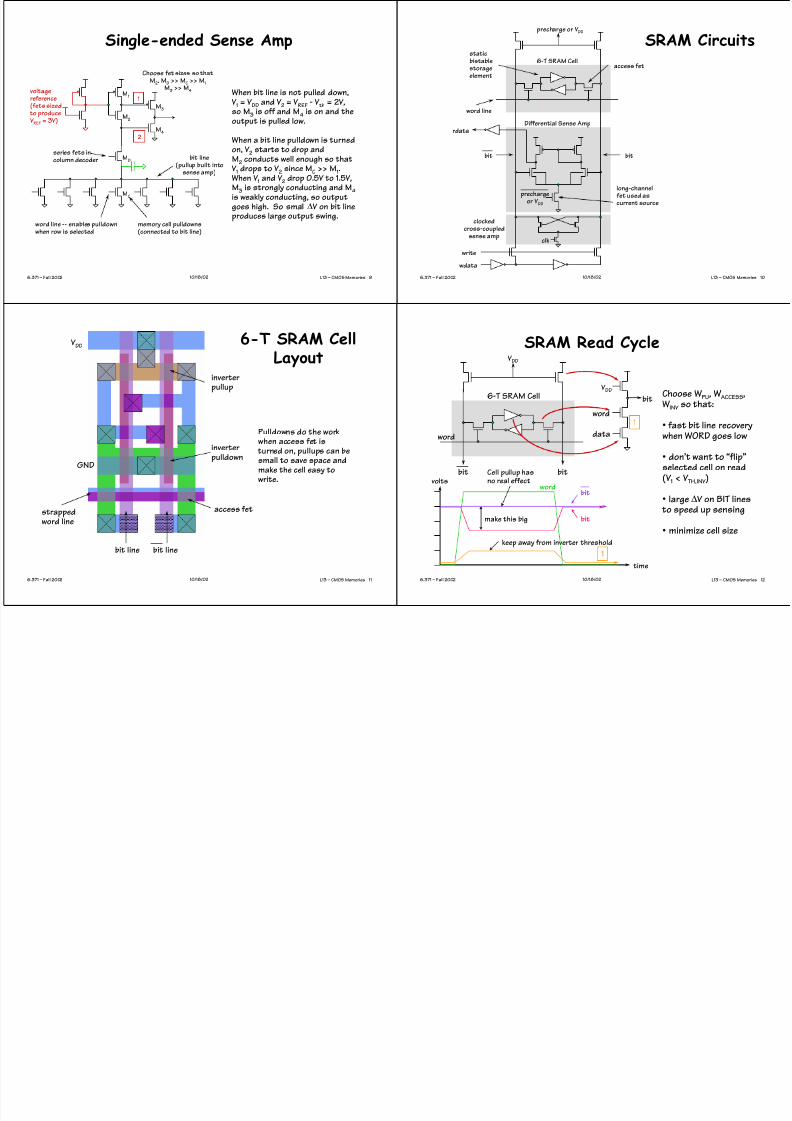
Single-ended Sense Amp
series fets incolumn decoder
memory cell pulldowns(connected to bit line)
bit line(pullup built into
sense amp)
word line -- enables pulldownwhen row is selected
voltagereference
(fets sized to produceV REF = 3V)
M1
M2
M3
M 4
MC
MD
1
2
Choose fet sizes so thatM2, MD >> MC >> M1
M3 >> M 4 When bit line is not pulled down,
V 1 = V DD and V 2 = V REF - V th = 2V,so M3 is off and M 4 is on and theoutput is pulled low.
When a bit line pulldown is turnedon, V 2 starts to drop andM2 conducts well enough so thatV 1 drops to V 2 since MC >> M1.When V 1 and V 2 drop 0.5V to 1.5V,M3 is strongly conducting and M 4is weakly conducting, so outputgoes high. So small ∆V on bit lineproduces large output swing.
L13 – CMOS Memories 106.371 – Fall 2002 10/18/02
SRAM Circuitsprecharge or V DD
6-T SRAM Cell
word line
Differential Sense Amp
write
wdata
bit bit
access fet
staticbistablestorageelement
long-channel fet used ascurrent source
prechargeor V DD
clk
clockedcross-coupled
sense amp
rdata
L13 – CMOS Memories 116.371 – Fall 2002 10/18/02
6-T SRAM CellLayout
inverterpullup
inverterpulldown
access fetstrappedword line
V DD
GND
bit line bit line
Pulldowns do the workwhen access fet is turned on, pullups can besmall to save space andmake the cell easy towrite.
L13 – CMOS Memories 126.371 – Fall 2002 10/18/02
SRAM Read CycleV DD
6-T SRAM Cell
bit bit
word
word
bit
V DD
data 1
wordbit
bit
1
volts
time
Choose W PU, W ACCESS,W INV so that:
fast bit line recoverywhen WORD goes low
• don’t want to “flip”selected cell on read(V 1 < V TH,INV )
• large ∆V on BIT lines to speed up sensing
•
minimize cell size
make this big
keep away from inverter
threshold
Cell pullup hasno real effect

8/6/2019 L13-4up Memory RAM
http://slidepdf.com/reader/full/l13-4up-memory-ram 4/5
L13 – CMOS Memories 136.371 – Fall 2002 10/18/02
DifferentialSense Amp
bit bit
long-channel fet used ascurrent “source”
V DD
rdata
4.8/0.6 4.8/0.6
4.8/0.6 4.8/0.6
0.9/7.2
V2 V1
VCS
12
3
L13 – CMOS Memories 146.371 – Fall 2002 10/18/02
Fast Address Decoding
Logically, row/columndecoders can be built from
wide fan-in AND gates. But these are slow, place heavyloading on address wires andmay be hard to fit into thepitch of the memory cell.
A2 A1 A0 A2 A1 A0
One can use predecode logic todecode blocks of addresses which
are then further decoded usingsmaller AND gates. The addresslines going to the predecode gatesare less loaded and all gates havesmaller fanin⇒ decode happens faster. Layout works better too!
L13 – CMOS Memories 156.371 – Fall 2002 10/18/02
Multiport SRAM (register files)
write
wd wd
read0read1
rd0 rd1
One can increase the numberof SRAM ports by addingaccess transistors. Writesare usually double-ended;
single-ended reads can beused to save space.
An alternative design that can be easilyexpanded withoutworrying about
unintentionally flipping the cell on reads isshown to the right.
writeread0read1
PU = 2/1PD = 4/1
PU = 2/2PD = 2/3
4/1
5/1
2/1
2/1
wd rd1rd0
L13 – CMOS Memories 166.371 – Fall 2002 10/18/02
Content-addressable RAM
By adding two transistors to the 6-T SRAM cell one can form an XOR gate to compare the cell contents to data on the bit lines. The output of thislogic can drive a pulldown in a distributed NOR gate to form a word“match” signal for a content-addressable memory (CAM).
word
match
xor gate
This node goes highif data on bit linesdoesn’t match datain the cell.
This node will bepulled down if any bitof the word doesn’tmatch
Read and Write cycles: likebefore…
Match cycle: place data onbit lines but don’t assertword line.

8/6/2019 L13-4up Memory RAM
http://slidepdf.com/reader/full/l13-4up-memory-ram 5/5
L13 – CMOS Memories 17 6.371 – Fall 2002 10/18/02
CAM Architecture
The word match lines from the CAM array can be used as WORD lines ina companion RAM to read out other data associated with the tagstored in the CAM. Uses: fully-associative caches, translationlookaside buffers (TLBs), ...
F i g u r e 8 . 7
6 b f r o m W e s t e & E s h r a g h i a n
L13 – CMOS Memories 186.371 – Fall 2002 10/18/02
3-T Dynamic
Ram
rdata
write
read
wdata
3-T DRAM Cell
precharge
CW CRCC Data is stored on
CC. It’s not destroyedon read, but will leakaway through write
transistor. CW >> CC
Precharge happensbefore each r/w cycle.READ/WRITE andPRECHARGE dont’overlap.
READ:After precharge, CR is charged high.When READ is asserted CR is pulled low
if there’s a stored “1” or remainsunchanged if there’s a stored “0”. Asense amp is usually used to speed up the availability of read data.
WRITE:After precharge, CW is charged high.When WRITE is asserted CW shares charge
with CC and dominates since CW >> CC. If WDATA is asserted, both CW and CC will bedischarged, writing a “0” into the cell;otherwise a “1” will be written.
Pros: little or no static power, smaller than SRAMCons: needs refresh, need time to precharge
L13 – CMOS Memories 196.371 – Fall 2002 10/18/02
1-T DynamicRAM
TiN top electrode (V REF)
Ta2O5 dielectric
W bottomelectrode
polywordline
access fet
“Stack” DRAM Cell
1-T DRAM Cell
word
bit
access fet
Explicit storagecapacitor (fet gate, trench, stack) = 30fF to 100fF. If wewant higher C:
C =ε A
d
more areabetter dielectric
thinner film
V REF
L13 – CMOS Memories 206.371 – Fall 2002 10/18/02
1-T DRAMReadCycleC/2CC C CC/2
R1R2 R129 R130
DSL DSRPC
CS
PC PC
lbit rbit
V DDV DD
lbit, rbit
precharge (PC)
row sel (RN)
dummy sel (DSL,R)
column sel (CS)precharge bit lines,discharge dummy cells
read out bit, opposite dummy
amplify difference,restore bit cell
read out of dummy
cell half way between“0” and “1” value