l1 Mos Mosfet Operation
61
MOS capacitor operation
description
mosfet
Transcript of l1 Mos Mosfet Operation
MOS capacitor operation
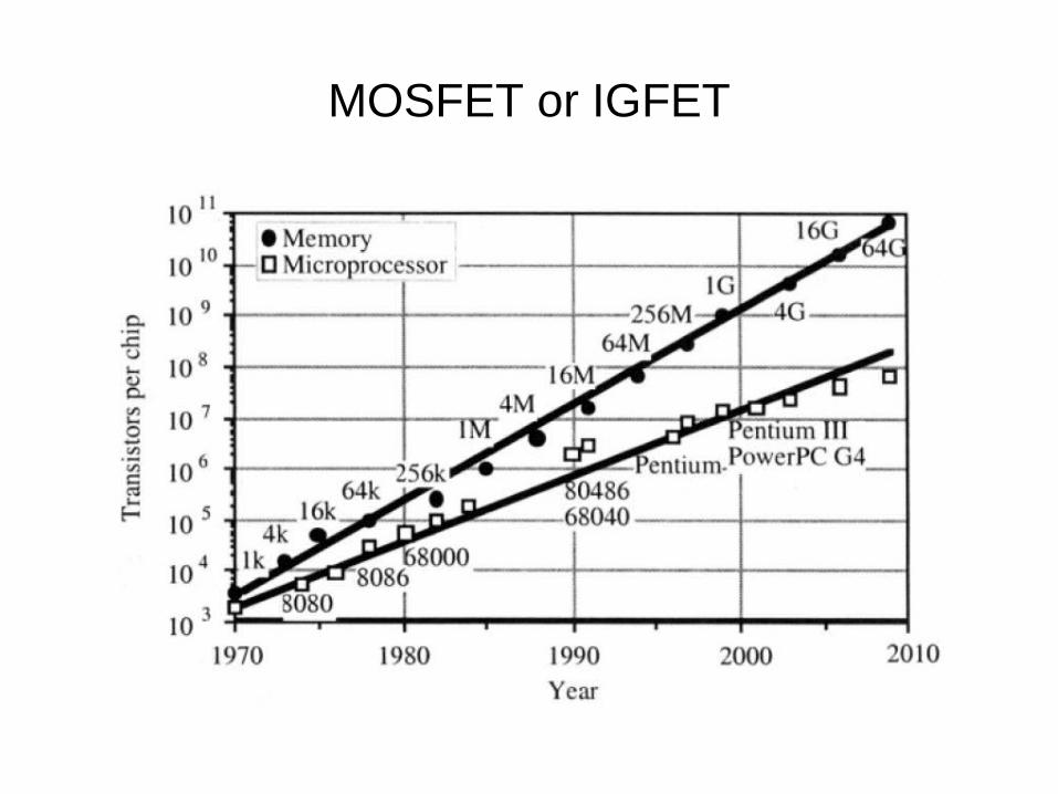
MOSFET or IGFET
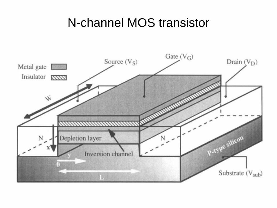
N-channel MOS transistor
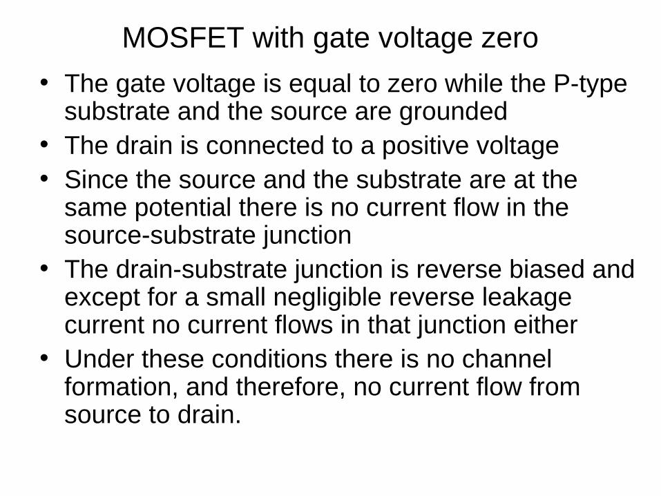
MOSFET with gate voltage zero
• The gate voltage is equal to zero while the P-type substrate and the source are grounded
• The drain is connected to a positive voltage • Since the source and the substrate are at the
same potential there is no current flow in the source-substrate junction
• The drain-substrate junction is reverse biased and except for a small negligible reverse leakage current no current flows in that junction either
• Under these conditions there is no channel formation, and therefore, no current flow from source to drain.
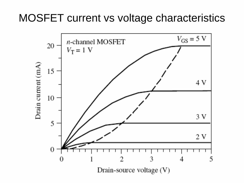
MOSFET current vs voltage characteristics
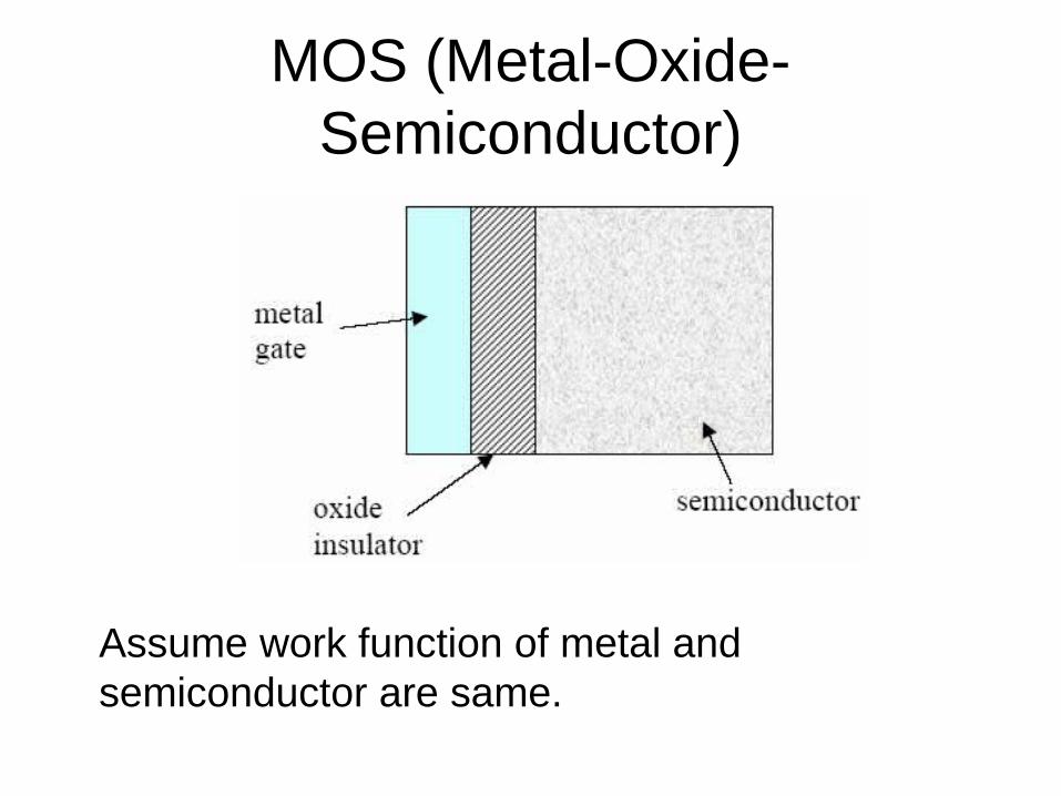
MOS (Metal-Oxide-Semiconductor)
Assume work function of metal and semiconductor are same.
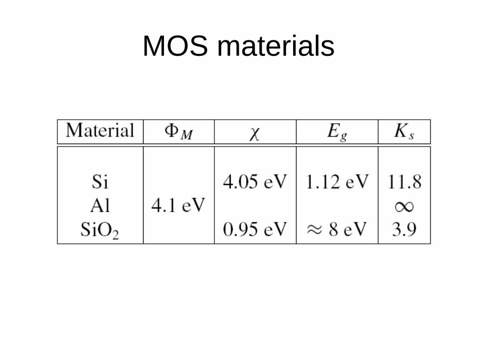
MOS materials
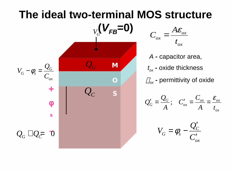
The ideal two-terminal MOS structure (VFB=0)
CG s
ox
QV
Cφ
′= −
′
oxox
ox
AC
t
ε=
; G ox oxG ox
ox
Q CQ C
A A t
ε′ ′= = =
A - capacitor area,
tox - oxide thickness
ox - permittivity of oxide
M
O
S+
φs
_
GG s
ox
QV
Cφ− =
CQ
GQ
0G CQ Q+ =
GV
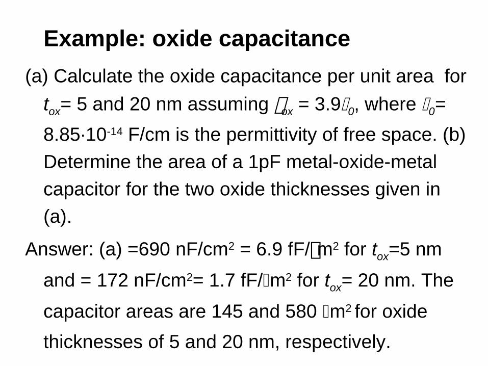
Example: oxide capacitance
(a) Calculate the oxide capacitance per unit area for
tox= 5 and 20 nm assuming ox = 3.90, where 0=
8.85·10-14 F/cm is the permittivity of free space. (b)
Determine the area of a 1pF metal-oxide-metal
capacitor for the two oxide thicknesses given in
(a).
Answer: (a) =690 nF/cm2 = 6.9 fF/m2 for tox=5 nm
and = 172 nF/cm2= 1.7 fF/m2 for tox= 20 nm. The
capacitor areas are 145 and 580 m2 for oxide
thicknesses of 5 and 20 nm, respectively.
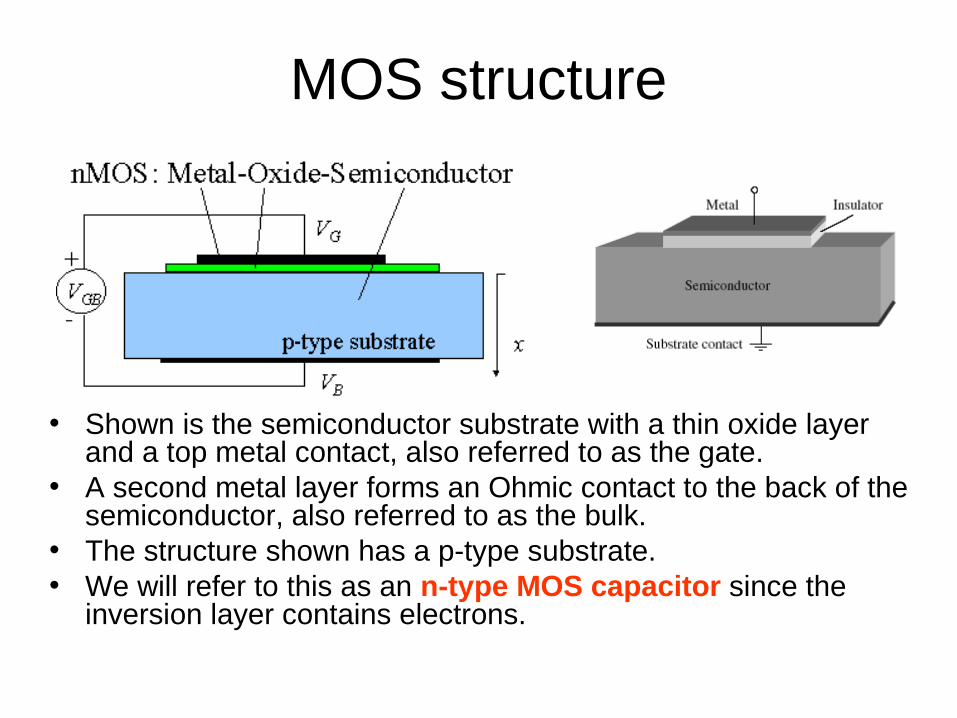
MOS structure
• Shown is the semiconductor substrate with a thin oxide layer and a top metal contact, also referred to as the gate.
• A second metal layer forms an Ohmic contact to the back of the semiconductor, also referred to as the bulk.
• The structure shown has a p-type substrate. • We will refer to this as an n-type MOS capacitor since the
inversion layer contains electrons.
Structure and principle of operation
• To understand the different bias modes of an MOS we consider 3 different bias voltages.
• (1) below the flatband voltage, VFB
• (2) between the flatband voltage and the threshold voltage, VT, and
• (3) larger than the threshold voltage. • These bias regimes are called the
accumulation, depletion and inversion mode of operation.
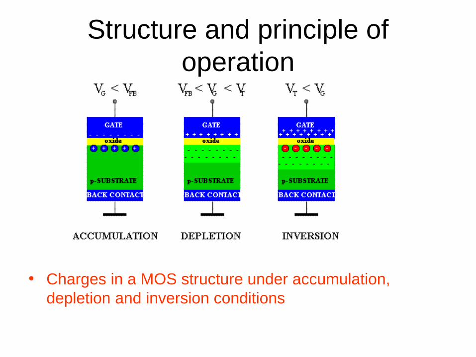
Structure and principle of operation
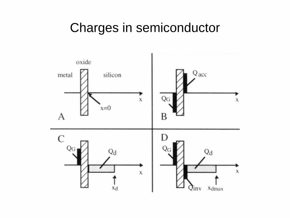
• Charges in a MOS structure under accumulation, depletion and inversion conditions
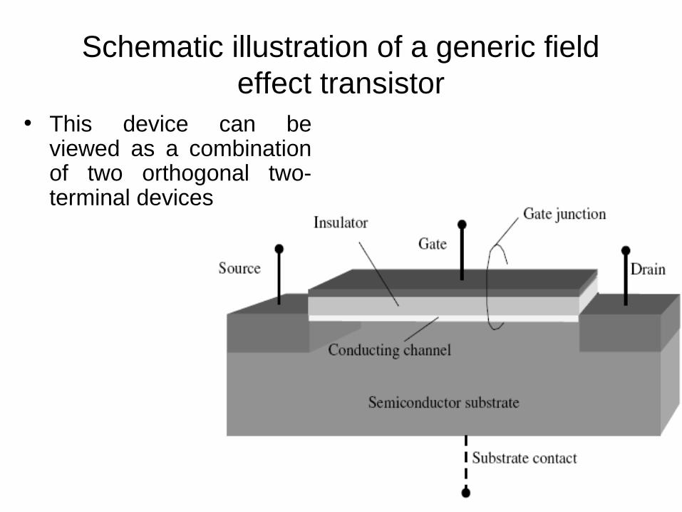
Schematic illustration of a generic field effect transistor
• This device can be viewed as a combination of two orthogonal two-terminal devices
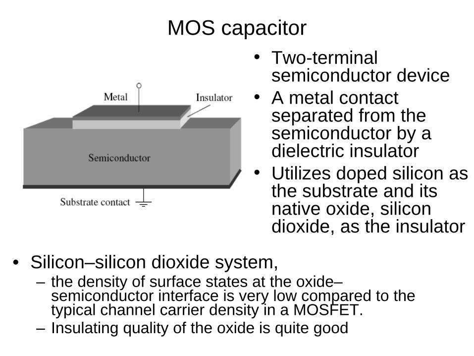
MOS capacitor• Two-terminal
semiconductor device• A metal contact
separated from the semiconductor by a dielectric insulator
• Utilizes doped silicon as the substrate and its native oxide, silicon dioxide, as the insulator
• Silicon–silicon dioxide system,– the density of surface states at the oxide–
semiconductor interface is very low compared to the typical channel carrier density in a MOSFET.
– Insulating quality of the oxide is quite good
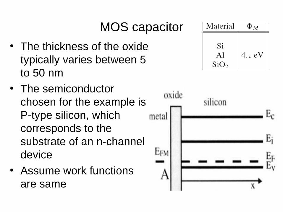
MOS capacitor
• The thickness of the oxide typically varies between 5 to 50 nm
• The semiconductor chosen for the example is P-type silicon, which corresponds to the substrate of an n-channel device
• Assume work functions are same
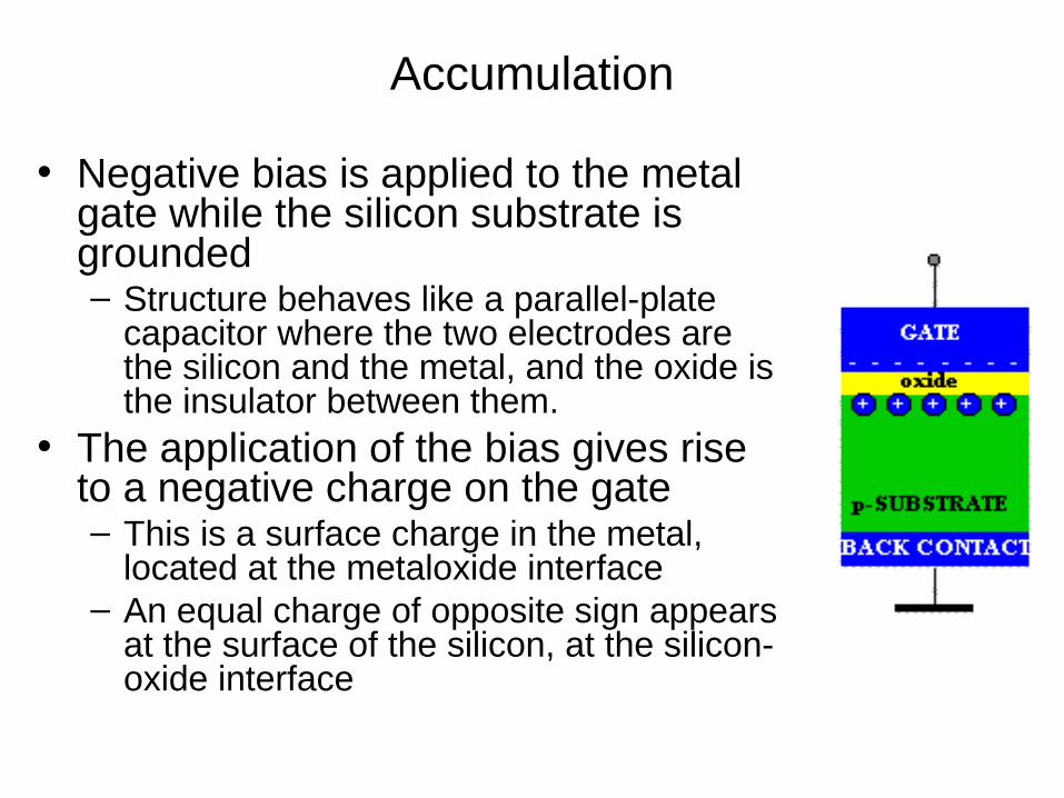
Accumulation
• Negative bias is applied to the metal gate while the silicon substrate is grounded – Structure behaves like a parallel-plate
capacitor where the two electrodes are the silicon and the metal, and the oxide is the insulator between them.
• The application of the bias gives rise to a negative charge on the gate– This is a surface charge in the metal,
located at the metaloxide interface– An equal charge of opposite sign appears
at the surface of the silicon, at the silicon-oxide interface
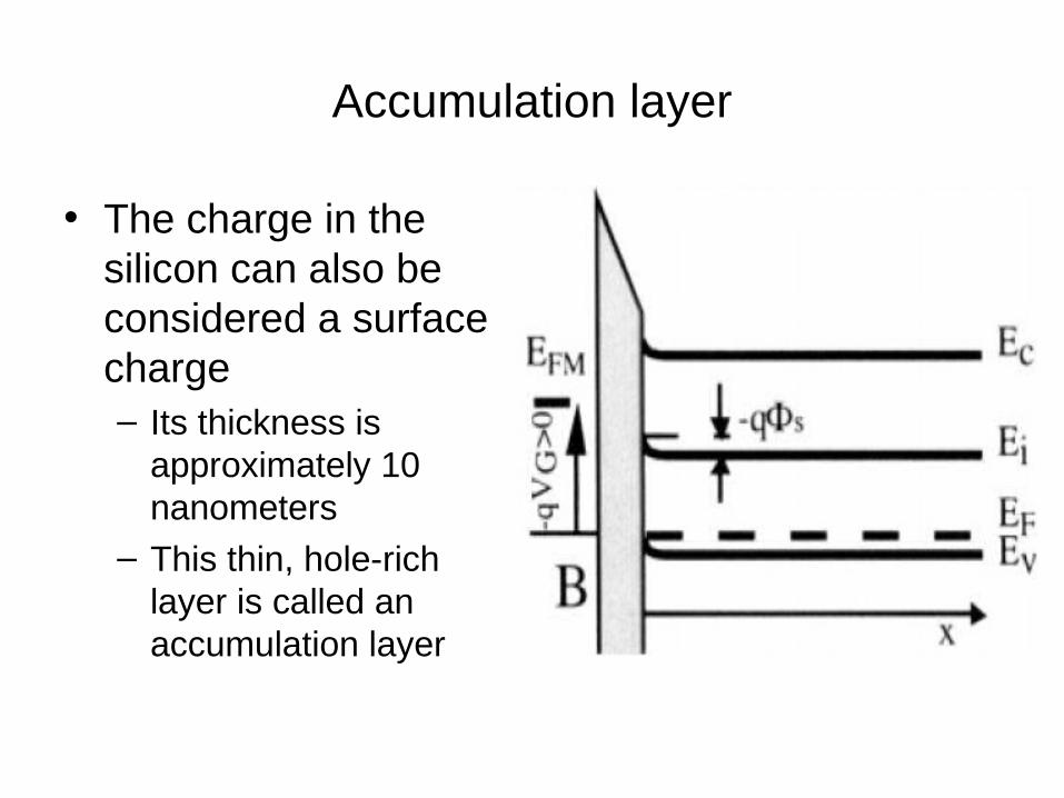
Accumulation layer
• The charge in the silicon can also be considered a surface charge– Its thickness is
approximately 10 nanometers
– This thin, hole-rich layer is called an accumulation layer
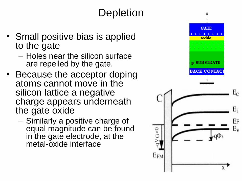
Depletion
• Small positive bias is applied to the gate– Holes near the silicon surface
are repelled by the gate. • Because the acceptor doping
atoms cannot move in the silicon lattice a negative charge appears underneath the gate oxide– Similarly a positive charge of
equal magnitude can be found in the gate electrode, at the metal-oxide interface
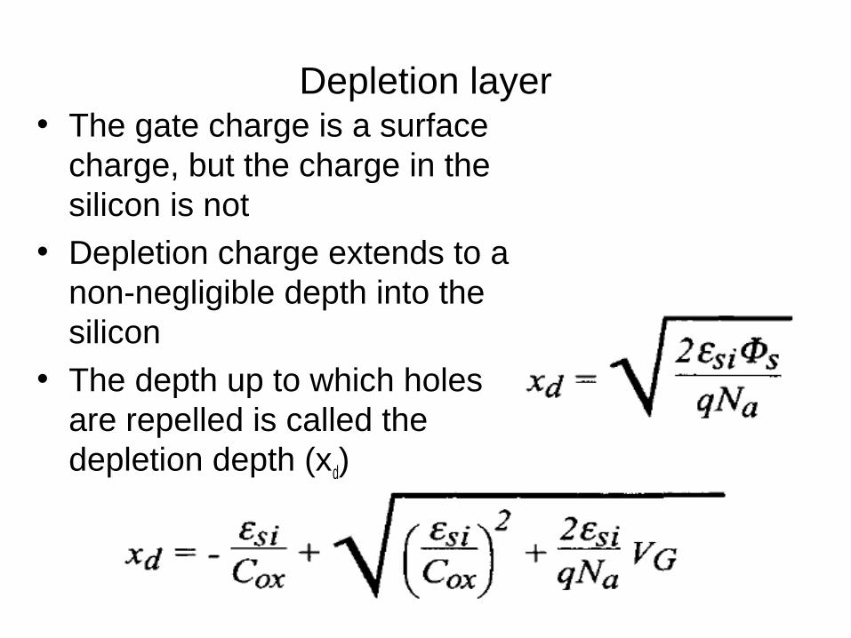
Depletion layer• The gate charge is a surface
charge, but the charge in the silicon is not
• Depletion charge extends to a non-negligible depth into the silicon
• The depth up to which holes are repelled is called the depletion depth (xd)
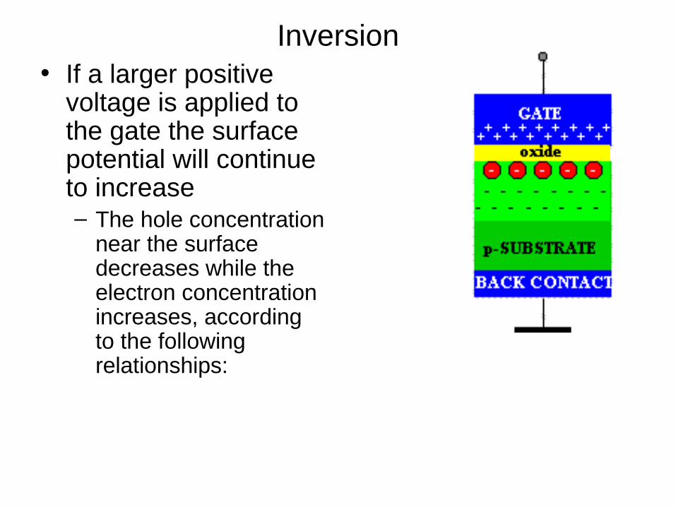
Inversion• If a larger positive
voltage is applied to the gate the surface potential will continue to increase– The hole concentration
near the surface decreases while the electron concentration increases, according to the following relationships:
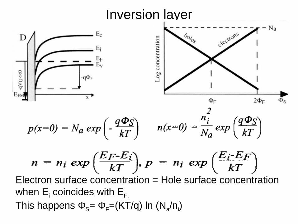
Inversion layer
Electron surface concentration = Hole surface concentration when Ei coincides with EF.
This happens ΦS= ΦF=(KT/q) ln (Na/ni)
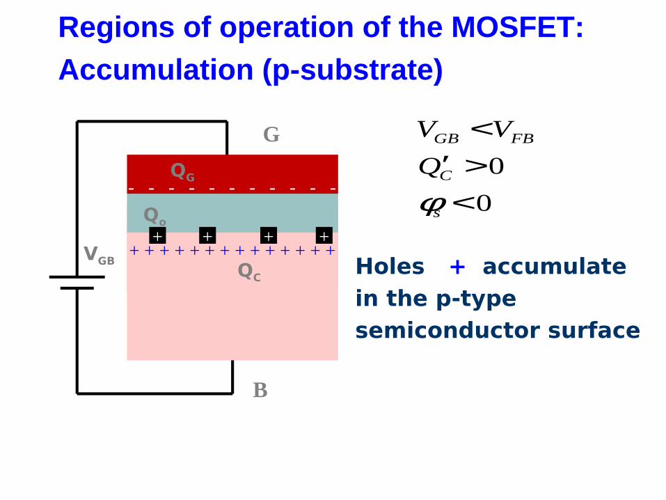
Regions of operation of the MOSFET:
Accumulation (p-substrate)
Holes + accumulate in the p-type semiconductor surface
0
0
GB FB
C
s
V V
Q
φ
<′ ><
+ + + + + + + + + + + + + +VGB
G
B
- - - - - - - - - - -
+ + + +Qo
QG
QC
VGB
G
B
+ + + + + + + + +
+ + + +Qo
QG
-- - -- -- -
-QC- -- --
φF = Fermi potential (defined in p-n junction lecture i.e. Ei-EF)
0
0
GB FB
C
s F
V V
Q
φ φ
>′ << <
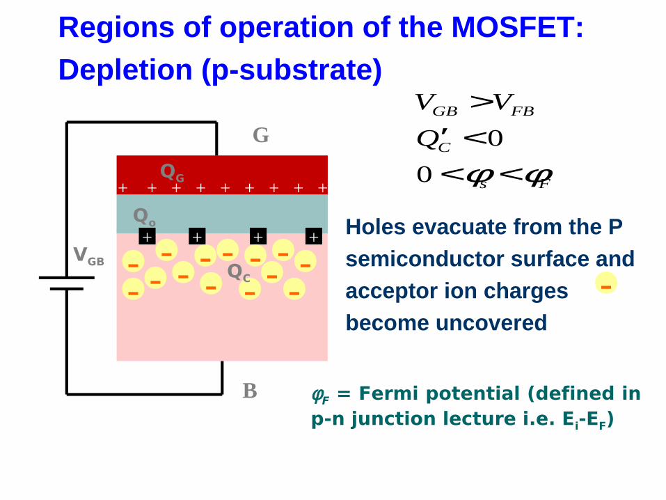
Holes evacuate from the P
semiconductor surface and
acceptor ion charges
become uncovered
-
Regions of operation of the MOSFET:
Depletion (p-substrate)
VGB
G
B
+ + + + + + + + +
+ + + +Qo
QG
-- - -- -- -
-QC- -- ---- - - - - --
-
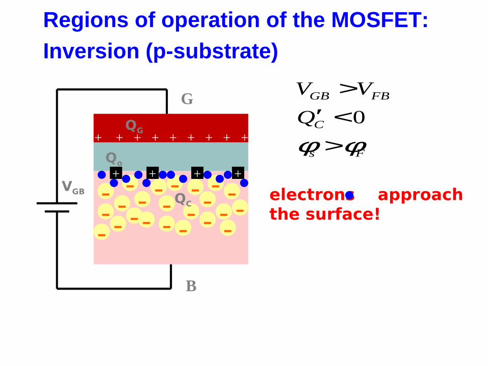
0GB FB
C
s F
V V
Q
φ φ
>′ <>
electrons approach the surface!
Regions of operation of the MOSFET:
Inversion (p-substrate)
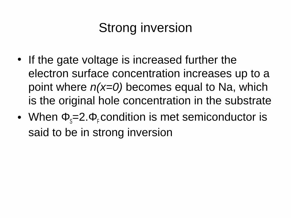
Strong inversion
• If the gate voltage is increased further the electron surface concentration increases up to a point where n(x=0) becomes equal to Na, which is the original hole concentration in the substrate
• When ΦS=2.ΦF condition is met semiconductor is said to be in strong inversion
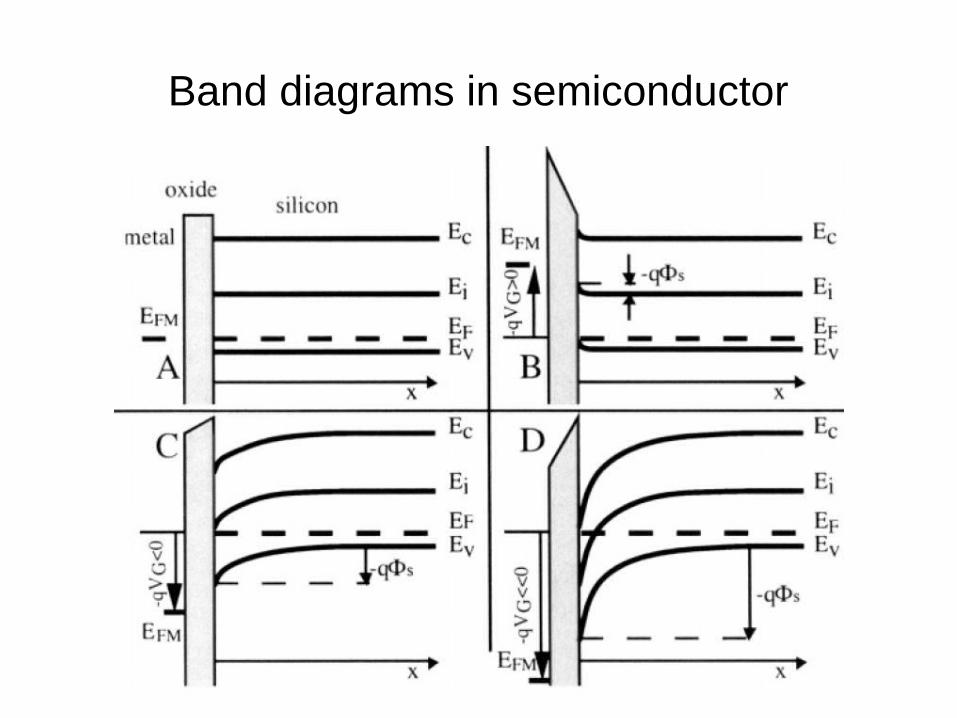
Band diagrams in semiconductor
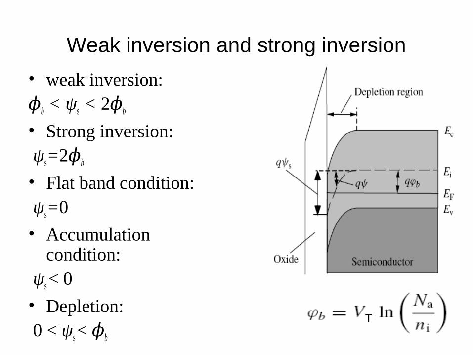
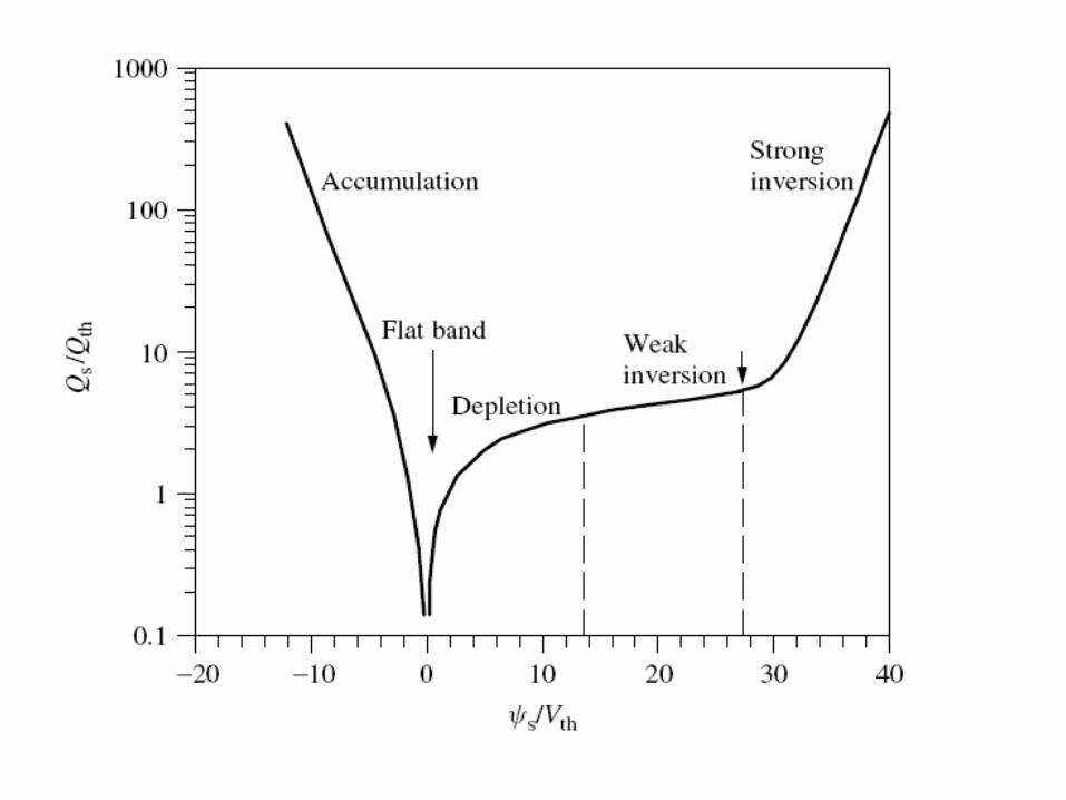
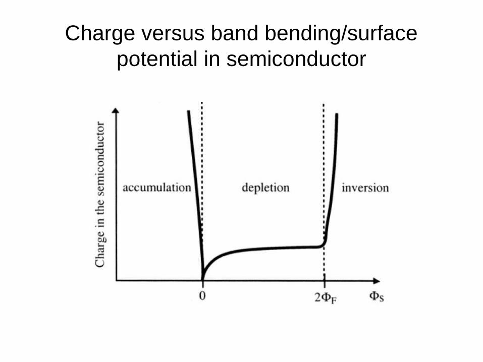
Weak inversion and strong inversion
• weak inversion: ϕb < ψs < 2ϕb
• Strong inversion: ψs=2ϕb
• Flat band condition: ψs=0
• Accumulation condition:
ψs < 0
• Depletion: 0 < ψs < ϕb
T
Charges in semiconductor
Charge versus band bending/surface potential in semiconductor
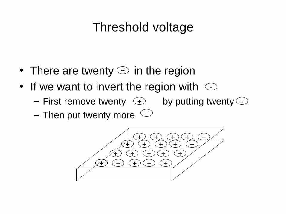
Threshold voltage
• There are twenty in the region• If we want to invert the region with
– First remove twenty by putting twenty
– Then put twenty more
+
-
-
-
+
++++++++++
++++++++++
++
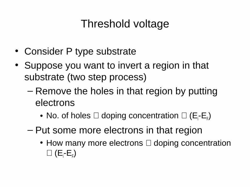
Threshold voltage
• Consider P type substrate• Suppose you want to invert a region in that
substrate (two step process)
– Remove the holes in that region by putting electrons
• No. of holes ∝ doping concentration ∝ (Ei-EF)
– Put some more electrons in that region• How many more electrons ∝ doping concentration
∝ (Ei-EF)
Threshold voltage
• Threshold voltage V = VT, corresponding to the onset of the strong inversion
• Strong inversion occurs when the surface potential ψs becomes equal to 2ϕb
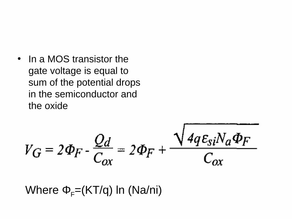
• In a MOS transistor the gate voltage is equal to sum of the potential drops in the semiconductor and the oxide
Where ΦF=(KT/q) ln (Na/ni)

Poly gate
• We have so far assumed that the Fermi level of the metal gate was equal to that of the silicon. In practice this is not the case
• In modern devices the gate material is not an actual metal, but heavily doped polycrystalline silicon, also called poly silicon
• The doping concentration used for that material is so high (1020/cm3) that it can be considered as a metal, for all practical purposes.
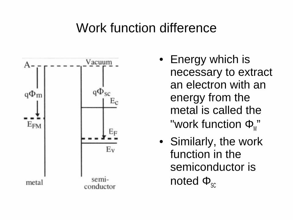
Work function difference
• Energy which is necessary to extract an electron with an energy from the metal is called the "work function ΦM”
• Similarly, the work function in the semiconductor is noted ΦSC
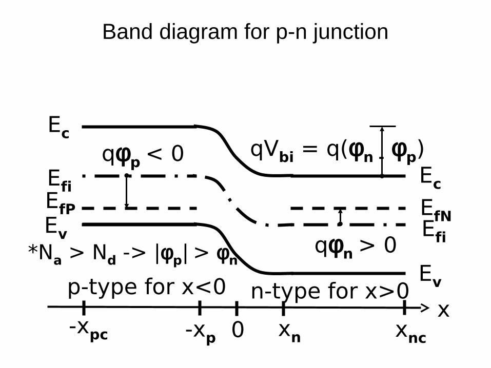
Band diagram for p-n junction
Ec
EfNEfi
Ev
Ec
EfP
Efi
Ev
0 xn
x-xp
-xpc xnc
qφp < 0
qφn > 0
qVbi = q(φn - φp)
*Na > Nd -> |φp| > φn
p-type for x<0 n-type for x>0
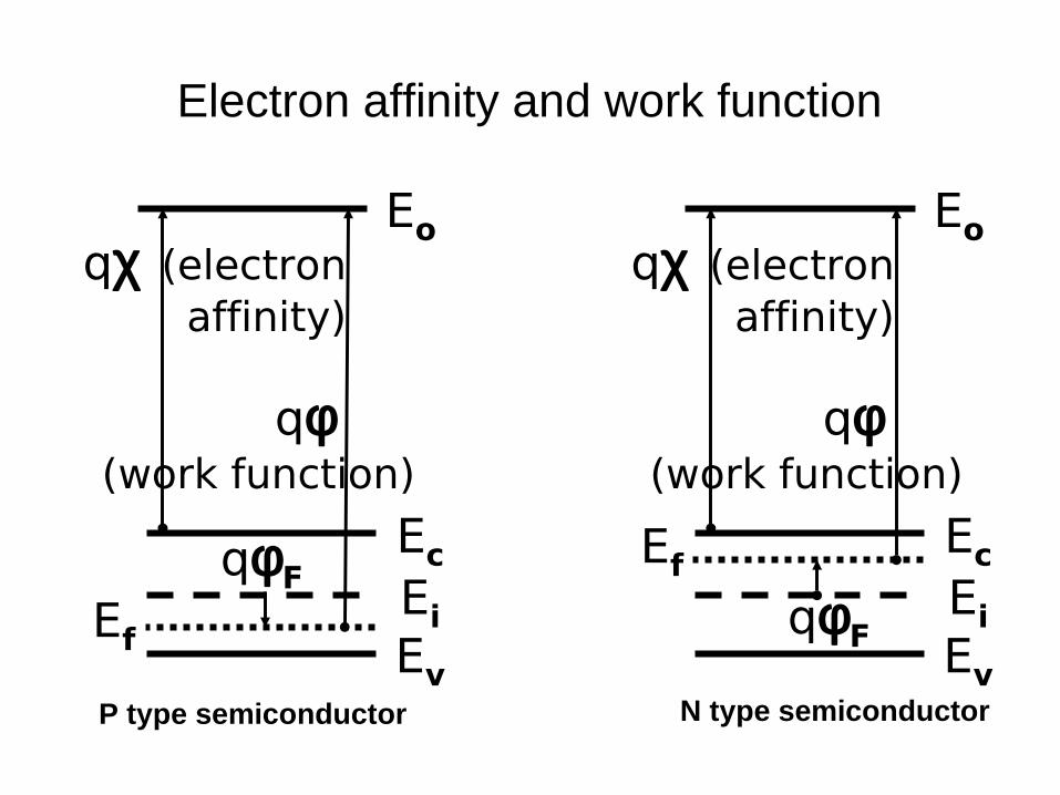
Electron affinity and work function
Eo
EcEfEi
Ev
qχ (electron affinity)
qφF
qφ(work function)
Eo
Ec
EfEi
Ev
qχ (electron affinity)
qφF
qφ(work function)
P type semiconductor N type semiconductor
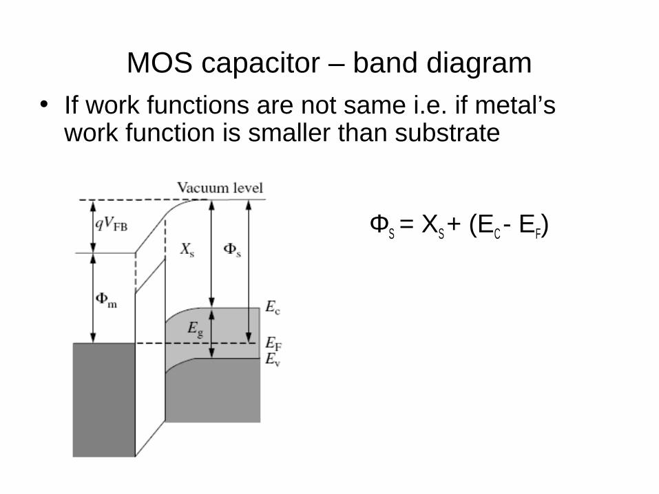
MOS capacitor – band diagram• If work functions are not same i.e. if metal’s
work function is smaller than substrate
ΦS = XS + (EC - EF)
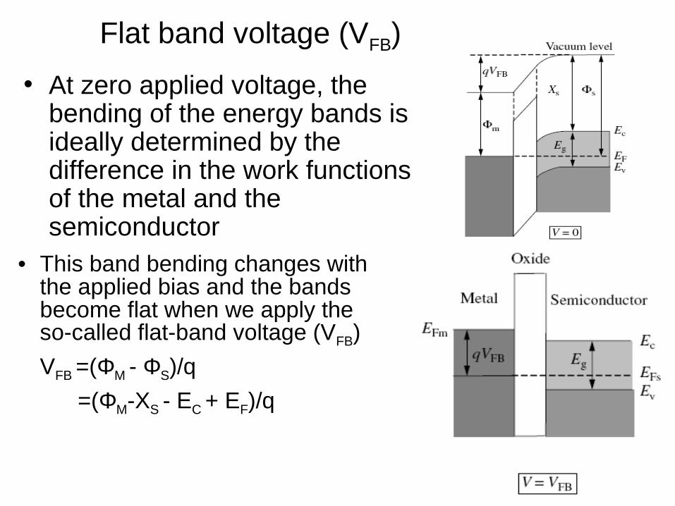
Flat band voltage (VFB)
• At zero applied voltage, the bending of the energy bands is ideally determined by the difference in the work functions of the metal and the semiconductor
• This band bending changes with the applied bias and the bands become flat when we apply the so-called flat-band voltage (VFB)
VFB =(ΦM - ΦS)/q
=(ΦM-XS - EC + EF)/q
MOS-Accumulation region
• Charge carriers same as that of substrate type getting accumulated near Si-SIO2 interface
• A MOS structure with a p-type semiconductor will enter the accumulation regime of operation when the voltage applied between the metal and the semiconductor is more negative than the flat-band voltage– If VFB is +0.5 V then accumulation region is below +0.5
V
– If VFB is -0.25 V then accumulation region is below -0.25 V
MOS – depletion region
• Assume MOS structure with a p-type substrate
• When V >VFB, the semiconductor–oxide interface first becomes depleted of holes and we enter the so-called depletion regime
MOS – inversion region
• For sufficiently larger voltages than VFB, we finally arrive at a situation in which the electron volume concentration at the interface exceeds the doping density in the semiconductor
• This is the strong inversion case in which we have a significant conducting sheet of inversion charge at the interface
Charges in the oxide
• Oxides grown on silicon contain positive charges due to the presence of contaminating metallic ions or imperfect Si-O bonds
• These charges can either be fixed or mobile in the oxide
• Mobile ions such as sodium and potassium can move in the presence of an electric field if the temperature is high enough
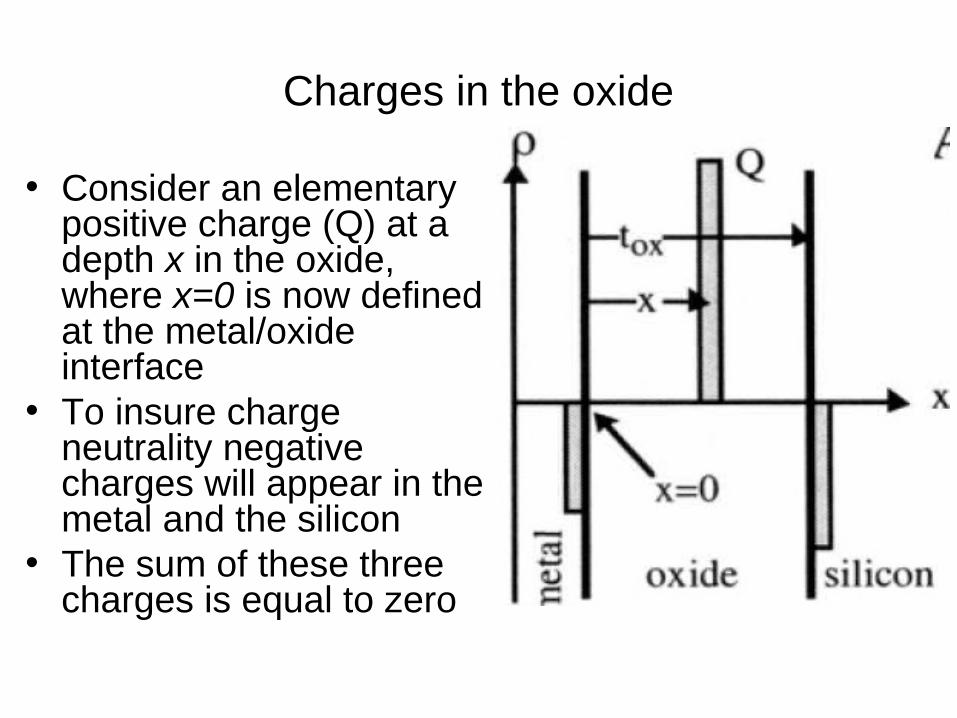
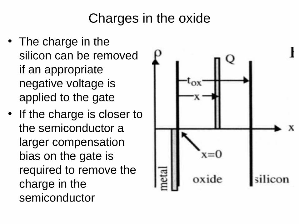
Charges in the oxide
• Consider an elementary positive charge (Q) at a depth x in the oxide, where x=0 is now defined at the metal/oxide interface
• To insure charge neutrality negative charges will appear in the metal and the silicon
• The sum of these three charges is equal to zero
Charges in the oxide
• The charge in the silicon can be removed if an appropriate negative voltage is applied to the gate
• If the charge is closer to the semiconductor a larger compensation bias on the gate is required to remove the charge in the semiconductor
Interface traps
• Presence of Si-SiO2 interface at the silicon surface introduces perturbation to the periodic crystal structure of the semiconductor– Causes some Si-Si bonds to be unfulfilled or "dangling"
• As a result there are energy states in the band gap at the silicon surface– These states are called "interface states" or "interface
traps“
• They can be charged positively or negatively, depending on their nature and their energy with respect to the Fermi level, and thus, will affect the surface potential
• To compensate for these charges, a bias must be applied to the gate
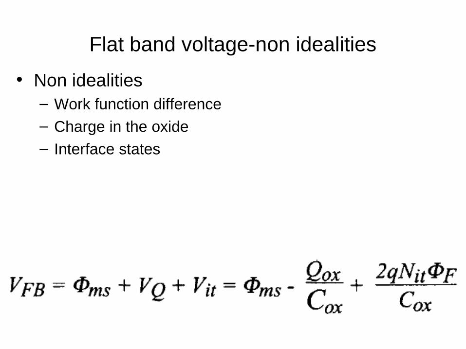
Flat band voltage-non idealities
• Non idealities– Work function difference
– Charge in the oxide
– Interface states
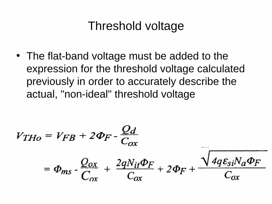
Threshold voltage
• The flat-band voltage must be added to the expression for the threshold voltage calculated previously in order to accurately describe the actual, "non-ideal" threshold voltage
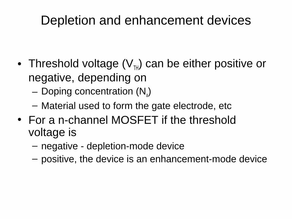
Depletion and enhancement devices
• Threshold voltage (VTH) can be either positive or negative, depending on– Doping concentration (Na)
– Material used to form the gate electrode, etc
• For a n-channel MOSFET if the threshold voltage is– negative - depletion-mode device– positive, the device is an enhancement-mode device
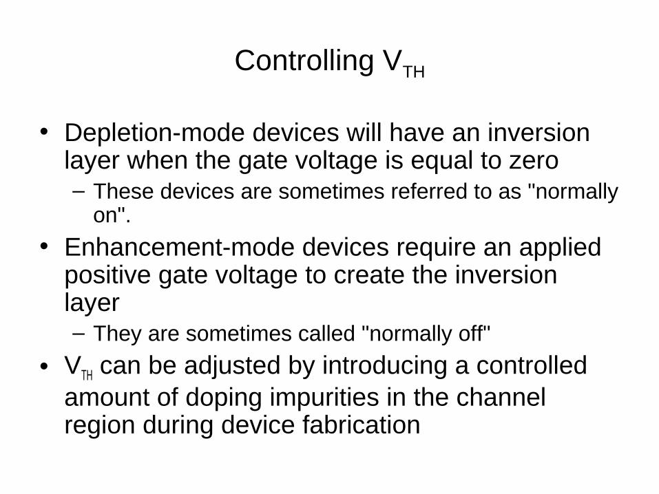
Controlling VTH
• Depletion-mode devices will have an inversion layer when the gate voltage is equal to zero– These devices are sometimes referred to as "normally
on".
• Enhancement-mode devices require an applied positive gate voltage to create the inversion layer– They are sometimes called "normally off"
• VTH can be adjusted by introducing a controlled amount of doping impurities in the channel region during device fabrication
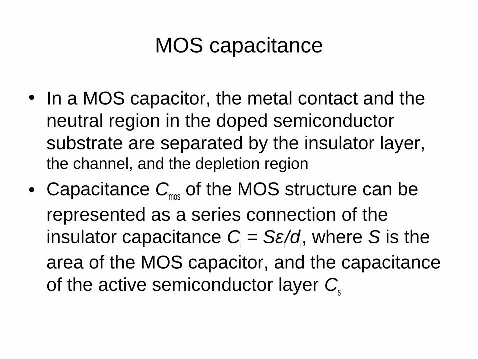
MOS capacitance
• In a MOS capacitor, the metal contact and the neutral region in the doped semiconductor substrate are separated by the insulator layer, the channel, and the depletion region
• Capacitance Cmos of the MOS structure can be represented as a series connection of the insulator capacitance Ci = Sεi/di, where S is the area of the MOS capacitor, and the capacitance of the active semiconductor layer Cs
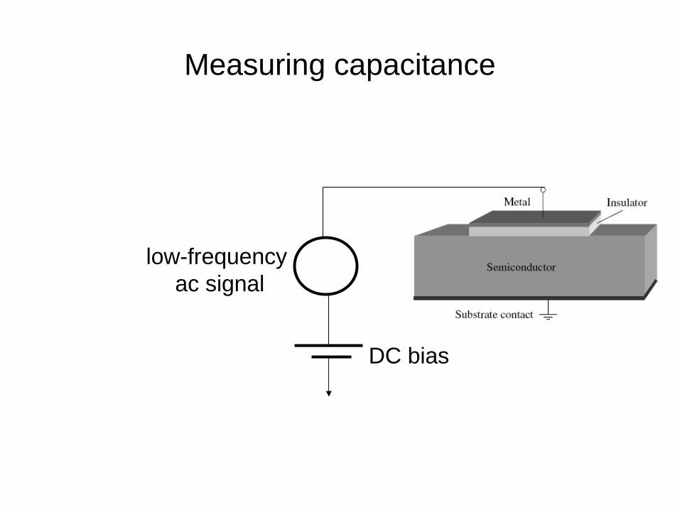
Measuring capacitance
DC bias
low-frequency ac signal
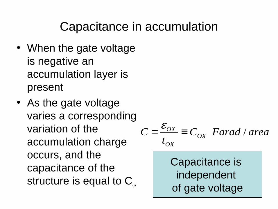
Capacitance in accumulation
• When the gate voltage is negative an accumulation layer is present
• As the gate voltage varies a corresponding variation of the accumulation charge occurs, and the capacitance of the structure is equal to Cox
areaFaradCt
C OXOX
OX /≡= ε
Capacitance is independent
of gate voltage
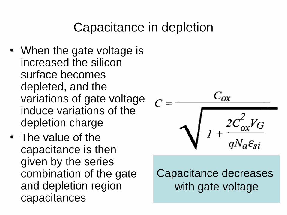
Capacitance in depletion
• When the gate voltage is increased the silicon surface becomes depleted, and the variations of gate voltage induce variations of the depletion charge
• The value of the capacitance is then given by the series combination of the gate and depletion region capacitances
Capacitance decreases with gate voltage
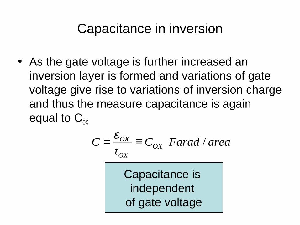
Capacitance in inversion
• As the gate voltage is further increased an inversion layer is formed and variations of gate voltage give rise to variations of inversion charge and thus the measure capacitance is again equal to COX
areaFaradCt
C OXOX
OX /≡= ε
Capacitance is independent
of gate voltage
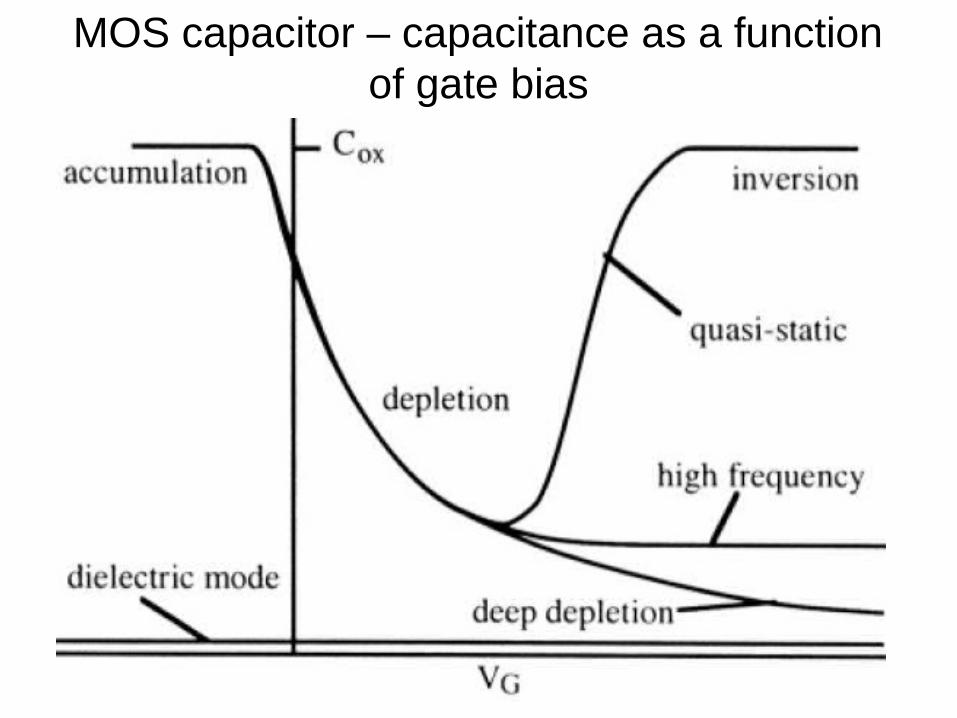
MOS capacitor – capacitance as a function of gate bias
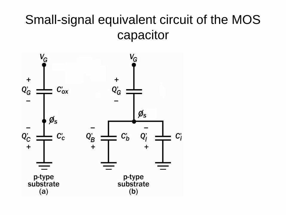
Small-signal equivalent circuit of the MOS capacitor
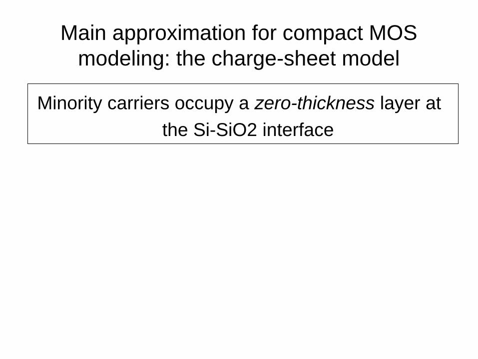
Main approximation for compact MOS modeling: the charge-sheet model
Minority carriers occupy a zero-thickness layer at
the Si-SiO2 interface
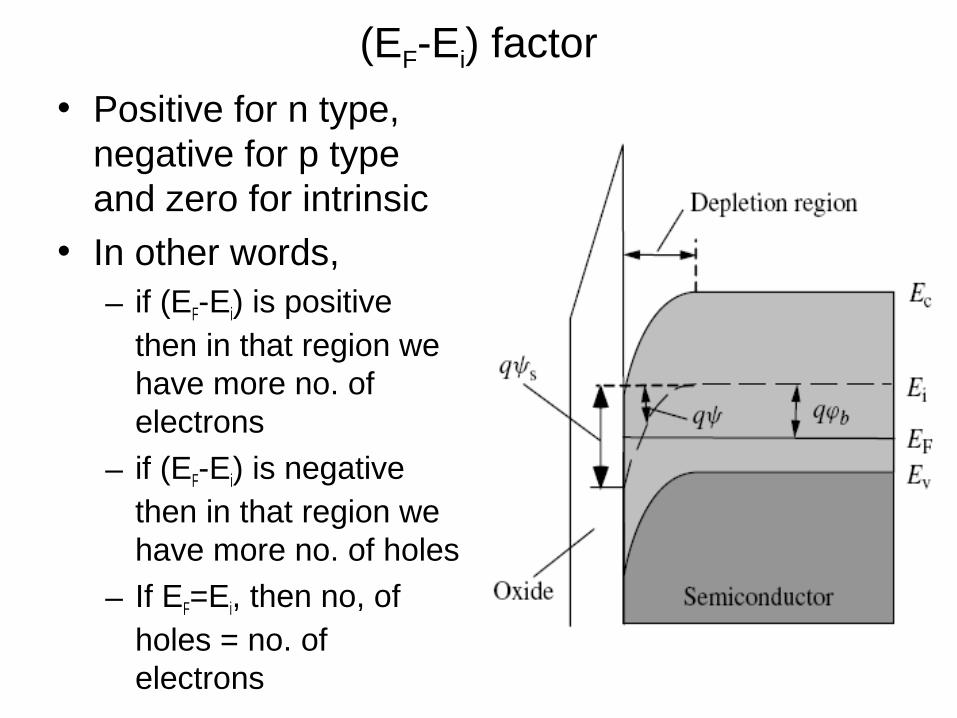
(EF-Ei) factor
• Positive for n type, negative for p type and zero for intrinsic
• In other words, – if (EF-Ei) is positive
then in that region we have more no. of electrons
– if (EF-Ei) is negative then in that region we have more no. of holes
– If EF=Ei, then no, of holes = no. of electrons

Weak inversion and strong inversion
• weak inversion: ϕb < ψs < 2ϕb
• Strong inversion: ψs=2ϕb
• Flat band condition: ψs=0
• Accumulation condition:
ψs < 0
• Depletion: 0 < ψs < ϕb
T