KTG783X -...
8
SS (1) GENERAL DESCRIPTION KTG783X series combines dedicated current mode PWM controller with a high voltage power MOSFET. It is GWtimized for high performance, low standby power, and cost effective off-line flyback converter applications in sub 20W range. series offers complete protection coverage with automatic self-recovery feature including Cycle-by-Cycle current limiting (OCP), over load protection (OLP), VDD over voltage clamp and under voltage lockout (UVLO). Excellent EMI performance is achieved with Power-Source proprietary frequency shuffling technique together with soft switching control at the totem poGW gate drive output. The tone energy at below 20KHZ is minimized in the design and audio noise is eliminated during operation. series is offered in SOP-8 & DIP8 package. FEATURES ■ Power on Soft Start Reducing MOSFET Vds Stress ■ Frequency shuffling for EMI ■ Extended Burst Mode Control For Improved Efficiency and Minimum Standby Power Design ■ Audio Noise Free Operation ■ Fixed 50KHZ Switching Frequency ■ Internal Synchronized Slope Compensation ■ Low VDD Startup Current and Low Operating Current ■ Leading Edge Blanking on Current Sense Input ■ Good Protection Coverage With Auto Self-Recovery VDD Over Voltage Clamp and Under Voltage Lockout with Hysteresis (UVLO) Y.SUN Proprietary Line Input Compensated Cycle-by-Cycle Over-current Threshold Setting For Constant Output Power Limiting Over Universal Input Voltage Range. Overload ProtectiGW (OLP). Over voltage Protection (OVP) ■ Pb-Free SOP-8L & DIP-8L APPLICATIONS Offline AC/DC flyback converter for ■ Battery Charger ■ PDA power supplies ■ Digital Cameras and Camcorder Adaptor ■ VCR, SVR, STB, DVD&DVCD Player SMPS ■ Set-Top Box Power ■ Auxiliary Power Supply for PC and Server ■ Open-frame SMPS TYPICAL APPLICATION KTG783X KTG783X KTG783X KTG783X
Transcript of KTG783X -...

SS
(1)
GENERAL DESCRIPTIONKTG783X series combines dedicated current mode PWM
controller with a high voltage power MOSFET. It is
GWtimized for high performance, low standby power, and
cost effective off-line flyback converter applications in sub
20W range.
series offers complete protection coverage with
automatic self-recovery feature including Cycle-by-Cycle
current limiting (OCP), over load protection (OLP), VDD
over voltage clamp and under voltage lockout (UVLO).
Excellent EMI performance is achieved with Power-Source
proprietary frequency shuffling technique together with soft
switching control at the totem poGW gate drive output.
The tone energy at below 20KHZ is minimized in the
design and audio noise is eliminated during operation.
series is offered in SOP-8 & DIP8 package.
FEATURES■ Power on Soft Start Reducing MOSFET Vds Stress
■ Frequency shuffling for EMI
■ Extended Burst Mode Control For Improved Efficiency
and Minimum Standby Power Design
■ Audio Noise Free Operation
■ Fixed 50KHZ Switching Frequency
■ Internal Synchronized Slope Compensation
■ Low VDD Startup Current and Low Operating Current
■ Leading Edge Blanking on Current Sense Input
■ Good Protection Coverage With Auto Self-Recovery
VDD Over Voltage Clamp and Under Voltage
Lockout with Hysteresis (UVLO)
Y.SUN Proprietary Line Input Compensated
Cycle-by-Cycle Over-current Threshold Setting
For Constant Output Power Limiting Over Universal
Input Voltage Range.
Overload ProtectiGW (OLP).
Over voltage Protection (OVP)
■ Pb-Free SOP-8L & DIP-8L
APPLICATIONSOffline AC/DC flyback converter for
■ Battery Charger
■ PDA power supplies
■ Digital Cameras and Camcorder Adaptor
■ VCR, SVR, STB, DVD&DVCD Player SMPS
■ Set-Top Box Power
■ Auxiliary Power Supply for PC and Server
■ Open-frame SMPS
TYPICAL APPLICATION
KTG783X
KTG783X
KTG783X
KTG783X
(2)
IC 封装 MOS Rdson(ohm) 最大输出功率(w) 85-265Vac最大输出功率(w)
KTG7832 SOP-8 • 9 • 8 • 7
KTG7834 DIP-8 • 9 • 16 • 12
KTG7836 DIP-8 • 4 • 21 • 18
KTG7838 DIP-8 • 3.2 • 27 • 24
Parameter Value
Drain Voltage (off state) -0.3V to 650V
VDD Voltage -0.3V to 30V
VDD-G Input Voltage -0.3V to 30V
VDD Clamp Continuous Current 10 mA
FB Input Voltage -0.3 to 7V
Sense Input Voltage -0.3 to 7V
Min/Max Operating Junction Temperature TJ -20 to 150℃
Min/Max Storage Temperature Tstg -55 to 160℃
Lead Temperature (Soldering,10secs) 260℃
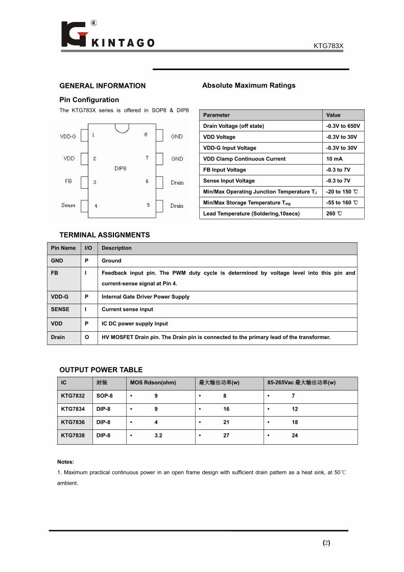
Pin Name I/O Description
GND P Ground
FB I Feedback input pin. The PWM duty cycle is determined by voltage level into this pin and
current-sense signal at Pin 4.
VDD-G P Internal Gate Driver Power Supply
SENSE I Current sense input
VDD P IC DC power supply input
Drain O HV MOSFET Drain pin. The Drain pin is connected to the primary lead of the transformer.
SOP8
DIP8
Absolute Maximum Ratings
TERMINAL ASSIGNMENTS
Pin ConfigurationThe series is offered in SOP8 & DIP8
package as shown below.
GENERAL INFORMATION
OUTPUT POWER TABLE
Notes:
1. Maximum practical continuous power in an open frame design with sufficient drain pattern as a heat sink, at 50℃
ambient.
KTG783X
KTG783X
(3)
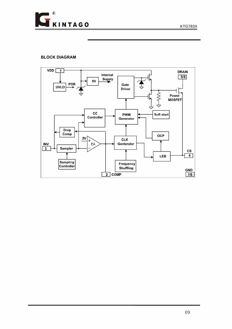
BLOCK DIAGRAM
KTG783X
(4)
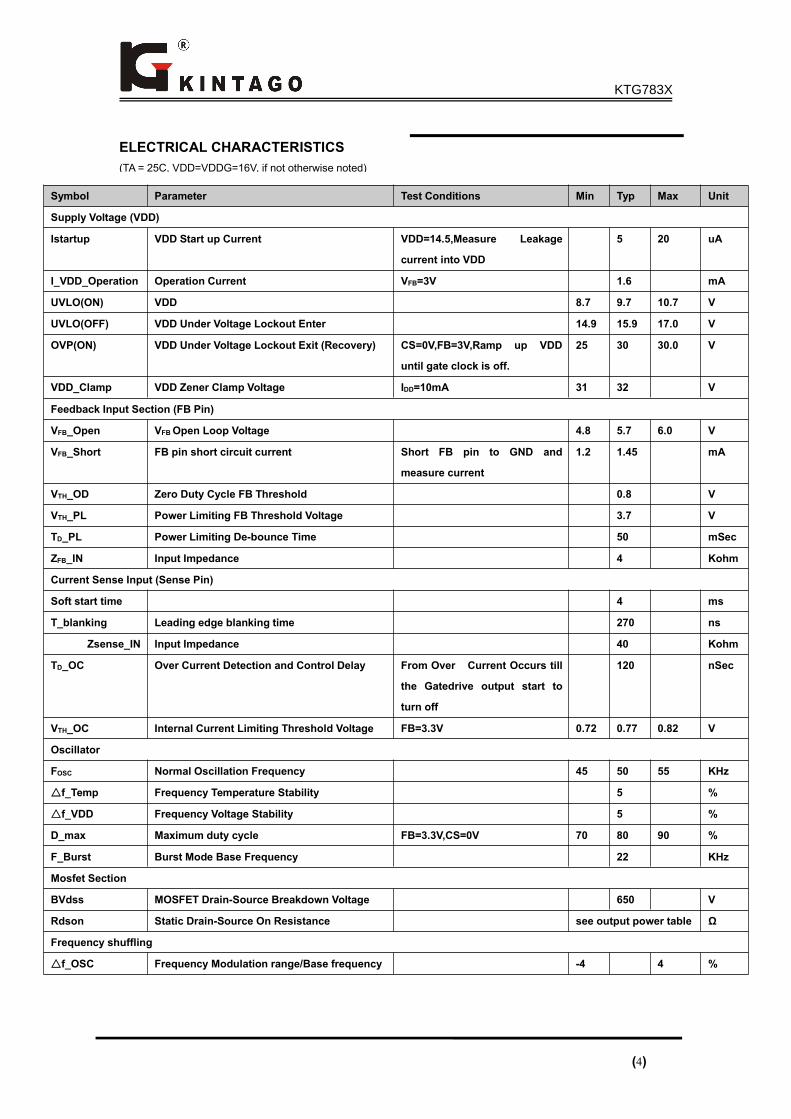
Symbol Parameter Test Conditions Min Typ Max Unit
Supply Voltage (VDD)
Istartup VDD Start up Current VDD=14.5,Measure Leakage
current into VDD
5 20 uA
I_VDD_Operation Operation Current VFB=3V 1.6 mA
UVLO(ON) VDD 8.7 9.7 10.7 V
UVLO(OFF) VDD Under Voltage Lockout Enter 14.9 15.9 17.0 V
OVP(ON) VDD Under Voltage Lockout Exit (Recovery) CS=0V,FB=3V,Ramp up VDD
until gate clock is off.
25 30 30.0 V
VDD_Clamp VDD Zener Clamp Voltage IDD=10mA 31 32 V
Feedback Input Section (FB Pin)
VFB_Open VFBOpen Loop Voltage 4.8 5.7 6.0 V
VFB_Short FB pin short circuit current Short FB pin to GND and
measure current
1.2 1.45 mA
VTH_OD Zero Duty Cycle FB Threshold 0.8 V
VTH_PL Power Limiting FB Threshold Voltage 3.7 V
TD_PL Power Limiting De-bounce Time 50 mSec
ZFB_IN Input Impedance 4 Kohm
Current Sense Input (Sense Pin)
Soft start time 4 ms
T_blanking Leading edge blanking time 270 ns
Zsense_IN Input Impedance 40 Kohm
TD_OC Over Current Detection and Control Delay From Over Current Occurs till
the Gatedrive output start to
turn off
120 nSec
VTH_OC Internal Current Limiting Threshold Voltage FB=3.3V 0.72 0.77 0.82 V
Oscillator
FOSC Normal Oscillation Frequency 45 50 55 KHz
△f_Temp Frequency Temperature Stability 5 %
△f_VDD Frequency Voltage Stability 5 %
D_max Maximum duty cycle FB=3.3V,CS=0V 70 80 90 %
F_Burst Burst Mode Base Frequency 22 KHz
Mosfet Section
BVdss MOSFET Drain-Source Breakdown Voltage 650 V
Rdson Static Drain-Source On Resistance see output power table Ω
Frequency shuffling
△f_OSC Frequency Modulation range/Base frequency -4 4 %
ELECTRICAL CHARACTERISTICS(TA = 25C, VDD=VDDG=16V, if not otherwise noted)
KTG783X
(5)
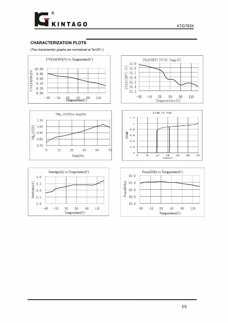
CHARACTERIZATION PLOTS(The characteristic graphs are normalized at Ta=25℃)
KTG783X

(6)
The switch frequency reduces at light/no load conditionto improve the conversion efficiency. At light load or noload condition, the FB input drops below burst modethreshold level and device enters Burst Mode control.The Gate drive output switches only when VDD voltagedrops below a preset level and FB input is active tooutput an on state. Otherwise the gate drive remains atoff state to minimize the switching loss and reduces thestandby power consumption to the greatest extend.
The switching frequency control also eliminates the
audio noise at any loading conditions.
Oscillator Operation
The switching frequencyof series internally
fixed at 50KHZ. No external frequency setting
components are required for PCB design simplification.
Current Sensing and Leading Edge Blanking
Cycle-by-Cycle current limiting is offered in
series current mode PWM control. The switch current is
detected by a sense resistor into the sense pin. An
internal leading edge blanking circuit chops off the
sensed voltage spike at initial internal power MOSFET
on state due to snubber diode reverse recovery and
surge gate current of internal power MOSFET so that
the external RC filtering on sense input is no longer
needed. The current limiting comparator is disabled and
cannot turn off the internal power MOSFET during the
blanking period. The PWM duty cycle is determined by
the current sense input voltage and the FB input voltage.
Internal Synchronized Slope CompensationBuilt-in slope compensation circuit adds voltage ramp
onto the current sense input voltage for PWM
generation. This greatly improves the close loop stability
at CCM and prevents the sub-harmonic oscillation and
thus reduces the output ripple voltage.
Drive
The internal power MOSFET series is driven
by a dedicated gate driver for power switch control. Too
weak the gate drive strength results in higher conduction
and switch loss of MOSFET while too strong gate drive
results the compromise of EMI.
OPERATION DESCRIPTION
The series is a low power off-line SMPSSwitcher optimized for off-line flyback converterapplications in sub 20W power range. The ‘Extendedburst mode’ control greatly reduces the standby powerconsumption and helps the design easily to meet theinternational power conservation requirements.
Startup Current and Start up ControlStartup current of series designed to be verylow so that VDD could be charged up above UVLOthreshold level and device starts up quickly. A large valuestartup resistor can therefore be used to minimize thepower loss yet achieve a reliable startup in application.For AC/DC adaptor with universal input range design, a 2MΩ, 1/8 W startup resistor could be used together with aVDD capacitor to provide a fast startup and yet lowpower dissipation design solution.
Operating CurrentThe Operating current of series is low at 2mA.Good efficiency is achieved with series lowoperating current together with the ‘Extended burstmode’ control features.
Soft Startseries features an internal 4ms soft start to
soften the electrical stress occurring in the power supplyduring startup. It is activated during the power onsequence. As soon as VDD reaches UVLO(OFF), thepeak current is gradually increased from nearly zero tothe maximum level of 0.77V. Every restart up is followedby a soft start.
Frequency shuffling for EMI improvementThe frequency Shuffling (switching frequencymodulation) is implemented in series.Theoscillation frequency is modulated so that the toneenergy is spread out. The spread spectrum minimizesthe conduction band EMI and therefore eases the systemdesign.
Extended Burst Mode OperationAt light load or zero load condition, most of the powerdissipation in a switching mode power supply is fromswitching loss on the mosfet, the core loss of theransformer and the loss on the snubber circuit. Themagnitude of power loss is in proportion to the switchingfrequency. Lower switching frequency leads to thereduction on the power loss and thus conserves theenergy. The switching frequency is internally adjusted atno load or light load condition.
KTG783X
KTG783X
KTG783X
KTG783XKTG783X
KTG783X
KTG783X
KTG783X
KTG783X
KTG783X
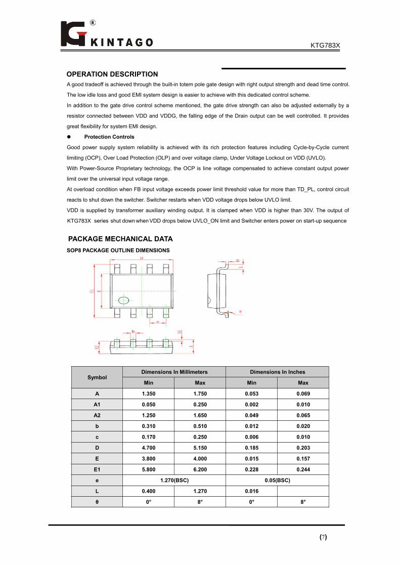
(7)
SymbolDimensions In Millimeters Dimensions In Inches
Min Max Min Max
A 1.350 1.750 0.053 0.069
A1 0.050 0.250 0.002 0.010
A2 1.250 1.650 0.049 0.065
b 0.310 0.510 0.012 0.020
c 0.170 0.250 0.006 0.010
D 4.700 5.150 0.185 0.203
E 3.800 4.000 0.015 0.157
E1 5.800 6.200 0.228 0.244
e 1.270(BSC) 0.05(BSC)
L 0.400 1.270 0.016
θ 0° 8° 0° 8°
A good tradeoff is achieved through the built-in totem pole gate design with right output strength and dead time control.
The low idle loss and good EMI system design is easier to achieve with this dedicated control scheme.
In addition to the gate drive control scheme mentioned, the gate drive strength can also be adjusted externally by a
resistor connected between VDD and VDDG, the falling edge of the Drain output can be well controlled. It provides
great flexibility for system EMI design.
Protection Controls
Good power supply system reliability is achieved with its rich protection features including Cycle-by-Cycle current
limiting (OCP), Over Load Protection (OLP) and over voltage clamp, Under Voltage Lockout on VDD (UVLO).
With Power-Source Proprietary technology, the OCP is line voltage compensated to achieve constant output power
limit over the universal input voltage range.
At overload condition when FB input voltage exceeds power limit threshold value for more than TD_PL, control circuit
reacts to shut down the switcher. Switcher restarts when VDD voltage drops below UVLO limit.
VDD is supplied by transformer auxiliary winding output. It is clamped when VDD is higher than 30V. The output of
series shut downwhenVDD drops below UVLO_ON limit and Switcher enters power on start-up sequence
OPERATION DESCRIPTION
PACKAGE MECHANICAL DATASOP8 PACKAGE OUTLINE DIMENSIONS
KTG783X
KTG783X
(8)
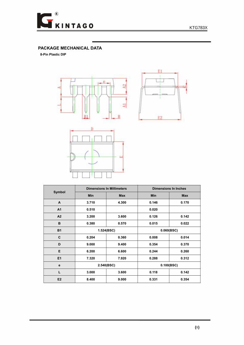
SymbolDimensions In Millimeters Dimensions In Inches
Min Max Min Max
A 3.710 4.300 0.146 0.170
A1 0.510 0.020
A2 3.200 3.600 0.126 0.142
B 0.380 0.570 0.015 0.022
B1 1.524(BSC) 0.060(BSC)
C 0.204 0.360 0.008 0.014
D 9.000 9.400 0.354 0.370
E 6.200 6.600 0.244 0.260
E1 7.320 7.920 0.288 0.312
e 2.540(BSC) 0.100(BSC)
L 3.000 3.600 0.118 0.142
E2 8.400 9.000 0.331 0.354
PACKAGE MECHANICAL DATA8-Pin Plastic DIP
KTG783X