kSA Emissometer Ex Situ Wafer arrier haracterization
8
The kSA Emissometer is designed to quickly and easily generate high- resoluon reflectance, emissivity and pocket-depth maps of wafer carriers. Wafer carrier emissivity variaon can mean temperature non- uniformity, which can lead to reduced device yield and possibly complete growth run failure. With the kSA Emissometer, emissivity changes can be tracked to determine carrier end-of-life without wasng growth runs. The kSA Emissometer also detects residual deposits aſter baking, and idenfies carrier surface defects, scratches, microcracks and pits. Applicaons: Wafer carrier emissivity and texture uniformity Quantave temperature set-point correcon, due to change in wafer carrier emissivity Detecon of residual material deposits Idenficaon of changes in pocket depth and profiles Carrier end-of-life determinaon kSA Emissometer Ex Situ Wafer Carrier Characterizaon Measures: Diffuse Reflectance Specular Reflectance Emissivity Pocket Depth Photoluminescence (oponal) k-Space Associates, Inc. | T: 734.426.7977 | [email protected] | k-space.com kSA Emissometer
Transcript of kSA Emissometer Ex Situ Wafer arrier haracterization

The kSA Emissometer is designed to quickly and easily generate high-
resolution reflectance, emissivity and pocket-depth maps of wafer
carriers. Wafer carrier emissivity variation can mean temperature non-
uniformity, which can lead to reduced device yield and possibly complete
growth run failure. With the kSA Emissometer, emissivity changes can be
tracked to determine carrier end-of-life without wasting growth runs. The
kSA Emissometer also detects residual deposits after baking, and identifies
carrier surface defects, scratches, microcracks and pits.
Applications:
Wafer carrier emissivity and texture uniformity
Quantitative temperature set-point correction, due to change in wafer carrier emissivity
Detection of residual material deposits
Identification of changes in pocket depth and profiles
Carrier end-of-life determination
kSA Emissometer
Ex Situ Wafer Carrier Characterization
Measures:
Diffuse Reflectance
Specular Reflectance
Emissivity
Pocket Depth
Photoluminescence (optional)
k-Space Associates, Inc. | T: 734.426.7977 | [email protected] | k-space.com
kSA Emissometer

kSA Emissometer Measurement Technology
kSA Emissometer: The kSA Emissometer uses a triple-sensor head for simultaneous height, diffuse reflectance and specular reflectance measurements as the wafer carrier rotates. The head moves on a linear scanning stage radially outward from the center of the carrier, acquiring data at user-specified radial steps to produce a real-time map of the carrier depth, diffuse reflectance, specular reflectance, and emissivity. The system features easy loading and unloading of carriers. An alignment laser allows alignment of carriers to a dimple or other carrier feature for reproducibility from scan to scan. The software interface is designed for operator or engineer use.
Scanning: The kSA Emissometer utilizes a high-resolution linear stage and fast data acquisition electronics to acquire complete carrier maps. Typical maps take measurements every 0.5 in 1mm radial steps, but the angular and radial resolution are user-programmable.
Depth: The depth of the carrier is measured via triangulation. The measured carrier depth is used to correct reflectance measurements for varying optical-head-to-carrier distances. It also provides carrier depth profiles for monitoring incoming wafer carriers and changes in carrier depth profiles with subsequent depositions.
Diffuse Reflectance: The diffuse reflectance of the carrier is measured from light incident at a 45 angle to the carrier and collected at normal incidence. The diffuse reflectance is the main component used to calculate the surface emissivity.
Specular Reflectance: The specular reflectance of the carrier is measured from light incident at a 45 angle to the carrier and collected at the corresponding 45 specularly reflected angle. The specular reflectance is typically small for SiC-coated wafer carriers. However, careful collection of the specular reflection signal provides details of surface imperfections like scratches, pits, and machining marks.
Emissivity: The point-by-point emissivity of the carrier is determined using the measured reflectance values at each point, i.e. by summing the diffuse and specular components of the reflectance. Variation in emissivity across the carrier can lead directly to temperature non-uniformity across the wafers.
Specular reflectance plot showing surface irregularities in the wafer pockets.
Diffuse reflectance plot showing defects at the edges of the wafer pockets.
k-Space Associates, Inc. | T: 734.426.7977 | [email protected] | k-space.com
2
Photograph of kSA Emissometer optical head geometry and scanning stage.

kSA Emissometer
kSA Emissometer Functional Specifications Specifications
Carrier Diameter Up to 800 mm
Carrier Compatibility Spindle centering, works with most commercially-available carriers
Scanning Stage Resolution 0.2 mm radial, 0.1 azimuthal, user-programmable
Scan Time 10 minutes (for a 0.1 and 1 mm resolution scan of a 465 mm carrier)
Reflectance / Emissivity
Detection Spot Size 1.5 mm
Light Source Wavelength 940 nm
Reflectance Resolution ± 0.005
Reflectance Accuracy ± 0.01
Emissivity Resolution ± 0.01
Emissivity Accuracy ± 0.02
Depth
Detection Spot Size 0.2 mm
Light Source Wavelength 660 nm
Depth Resolution ± 10 m
Depth Accuracy ± 10 m
k-Space Associates, Inc. | T: 734.426.7977 | [email protected] | k-space.com
3
UV Photoluminescence (PL): Characterization of MOCVD wafer carriers can be extended with the addition of an UV PL system to the kSA Emissometer. This option uses a LED focused at the wafer carrier and a filtered photodetector focused at the excitation point. The UV PL measurement tracks concurrent with the reflectivity/emissivity/height measurements and maps any features of residues and contaminants to the same positions mapped out with the standard analyses. Ask your k-Space representative to quote this option if you are interested in these capabilities.
UV PL map from carrier showing 2” AlN wafer as well as towel lint and other hydrocarbon residues.

The kSA Emissometer integrated software allows for easy control of the scan and in-depth analysis of the diffuse reflectance, specular reflectance, emissivity, and depth profile data. Data is easily exported to common data file types, as well as to common database formats (XML and JMP).
1 Partial diffuse reflectance carrier map. The diffuse reflectance is the main contributor to the emissivity calculation.
2 Partial specular reflectance carrier map. The specular reflectance is very sensitive to surface defects.
3 Partial emissivity carrier map. Note the emissivity variation across the wafer pockets.
4 Current carrier emissivity value at the current scan position, shown in real-time during the scan.
5 Scanning acquisition parameter dialogue. Enter the Run name, inner and outer radius values and the scan step size. Also select a user-defined analysis template for immediate carrier characterization results.
1 2 3
4 5
kSA Emissometer Integrated Software
kSA Emissometer software screen shot showing scanning dialogues and real-time data acquired from a wafer carrier scan.
k-Space Associates, Inc. | T: 734.426.7977 | [email protected] | k-space.com
4
kSA Emissometer
kSA Emissometer Analysis Features
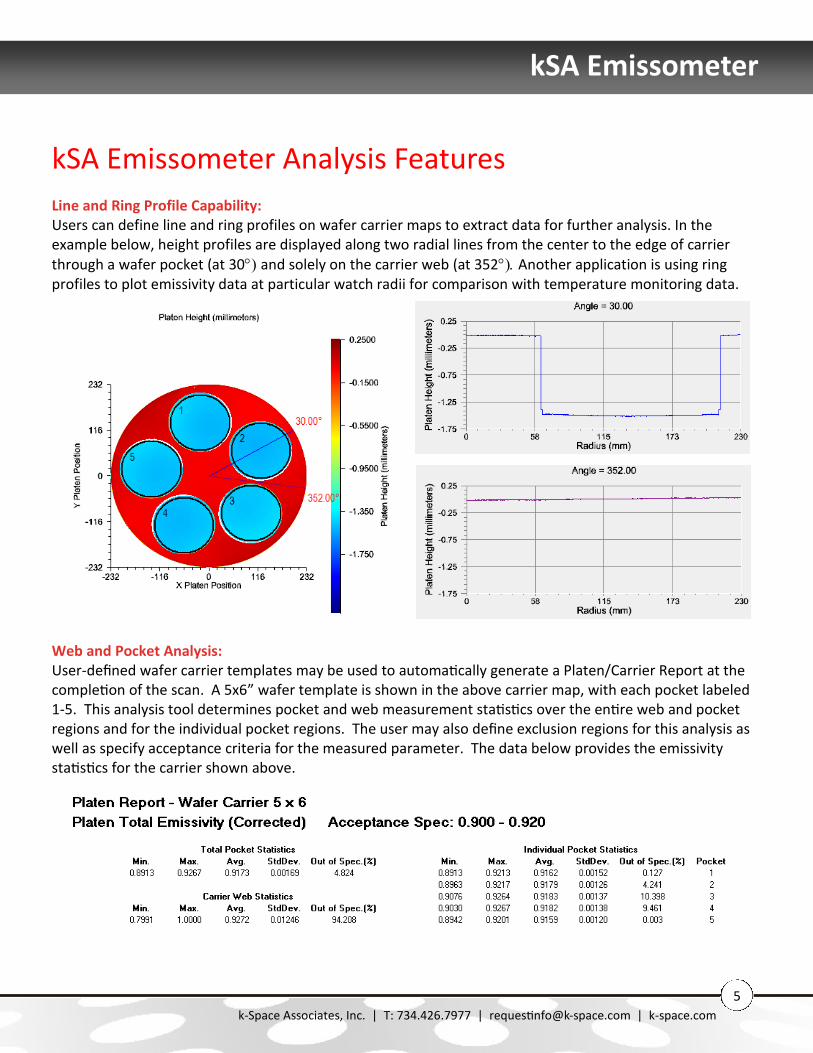
Line and Ring Profile Capability: Users can define line and ring profiles on wafer carrier maps to extract data for further analysis. In the example below, height profiles are displayed along two radial lines from the center to the edge of carrier through a wafer pocket (at 30) and solely on the carrier web (at 352) Another application is using ring profiles to plot emissivity data at particular watch radii for comparison with temperature monitoring data.
Web and Pocket Analysis: User-defined wafer carrier templates may be used to automatically generate a Platen/Carrier Report at the completion of the scan. A 5x6” wafer template is shown in the above carrier map, with each pocket labeled 1-5. This analysis tool determines pocket and web measurement statistics over the entire web and pocket regions and for the individual pocket regions. The user may also define exclusion regions for this analysis as well as specify acceptance criteria for the measured parameter. The data below provides the emissivity statistics for the carrier shown above.
k-Space Associates, Inc. | T: 734.426.7977 | [email protected] | k-space.com
5
k-Space Associates, Inc. | T: 734.426.7977 | [email protected] | k-space.com
6
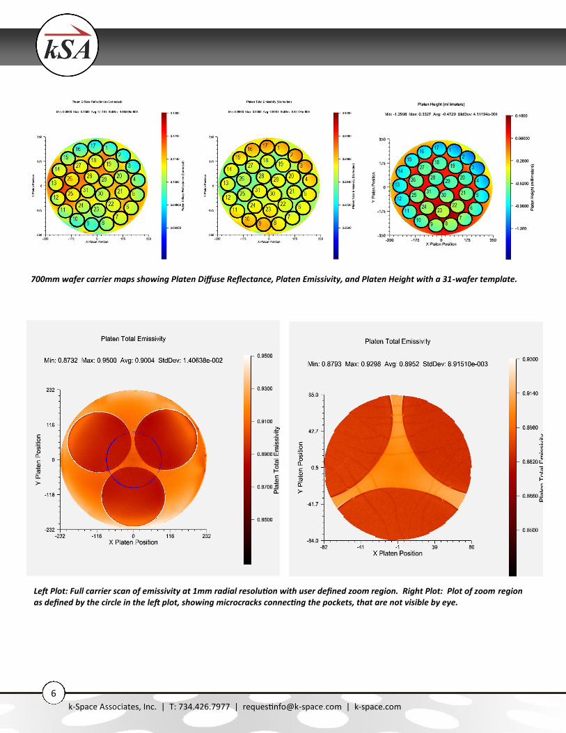
Left Plot: Full carrier scan of emissivity at 1mm radial resolution with user defined zoom region. Right Plot: Plot of zoom region as defined by the circle in the left plot, showing microcracks connecting the pockets, that are not visible by eye.
700mm wafer carrier maps showing Platen Diffuse Reflectance, Platen Emissivity, and Platen Height with a 31-wafer template.

kSA Emissometer
kSA Emissometer System Specifications
k-Space Associates, Inc. | T: 734.426.7977 | [email protected] | k-space.com
7
System Housing The kSA Emissometer is a standalone unit as shown below. The lid opens and the carrier rotational stage extends for easy carrier loading and unloading. The lid is closed during data collection to ensure high-quality measurements.
Controller The kSA Emissometer is supplied with a fully configured, Windows 10, multi-core CPU computer system mounted in the Emissometer enclosure. Supplied 22” LCD Monitor, keyboard and mouse sit outside the enclosure on an adjustable monitor arm. Please refer to the kSA Computer Product Specifications for the latest computer configuration. k-Space does not recommend customers substitute or update their own computer for the controller.
Facility Requirements Positioning: Four leveling casters are positioned on the bottom of the Emissometer. The unit can be rolled into place and then parked by lowering the feet so the casters are raised off the floor. System Power: 208 ‐240 VAC, 50/60Hz, single phase, 5 A max, with three wire for box mounting or user specified electrical connector. System Dimensions: Width=119cm, Depth=102cm, and Height=191cm with the lid closed and Height=241cm with the lid open. System Weight: 550kg (1212lbs).
Installation and Training A minimum of 1-2 days of installation and training are required.
Warranty All kSA systems and integrated components are warranted against defective materials and workmanship for a period of ONE YEAR from the date of delivery to the original purchaser.
Model of kSA Emissometer showing outer enclosure, wafer carrier placement, optical head
positioning, and integrated control electronics built into the bottom of the enclosure. (Computer
monitor arm and monitor not shown.)

Specifications are subject to change without notice. While due caution has been exercised in the production of this document, possible errors and omissions may occur.
kSA Emissometer Product Specification 15SEPT21
kSA Emissometer
k-Space has an expansive network of distributors to best serve our worldwide customer base.
HEADQUARTERS
k-Space Associates, Inc. Michigan, USA www.k-space.com [email protected]
DISTRIBUTION PARTNERS
RTA Instruments Ltd. Europe www.rta-instruments.com [email protected]
El Camino Technologies Pvt Ltd. India www.elcamino.in [email protected]
Giant Force Technology Co., Ltd. China www.giantforce.cn [email protected]
Jung Won Corporation South Korea www.jwc.co.kr [email protected]
R-DEC Co., Ltd. Japan Hong Kong
About k-Space Associates, Inc.
k-Space Associates, Inc., is a leading metrology supplier to the semiconductor, surface science, and thin-film technology industries.
Since 1992, we’ve delivered the most advanced thin-film characterization tools and software, thanks to close collaboration with
our worldwide customer base. We realize the best products are developed with our customers’ input, so we’re good listeners. For
your real-time surface analysis, curvature/stress, temperature, deposition rate, or custom project, we look forward to helping you
with your thin-film characterization needs.
k-Space Associates, Inc.
2182 Bishop Circle East Dexter, MI 48130 USA | T: 734.426.7977 | F: 734.426.7955 | request [email protected] | k-space.com