
KM3NeT front-end and readout electronics system: hardware ...
16
Sebastiano Aiello et al., “KM3NeT front-end and readout electronics system: hardware, firmware, and software, ” J. Astron. Telesc. Instrum. Syst. 5(4), 046001 (2019), doi: 10.1117/1.JATIS.5.4.046001. KM3NeT front-end and readout electronics system: hardware, firmware, and software Sebastiano Aiello Fabrizio Ameli Michel Andre Giorgos Androulakis Marco Anghinolfi Gisela Anton Miquel Ardid Julien Aublin Christos Bagatelas Giancarlo Barbarino Bruny Baret Suzan Basegmez du Pree Anastasios Belias Meriem Bendahman Edward Berbee Ad M. van den Berg Vincent Bertin Vincent van Beveren Simone Biagi Andrea Biagioni Matthias Bissinger Pascal Bos Jihad Boumaaza Simon Bourret Mohammed Bouta Gilles Bouvet Mieke Bouwhuis Cristiano Bozza Horea Brânza¸ s Max M. Briel Marc Bruchner Ronald Bruijn Jurgen Brunner Ernst-Jan Buis Raffaele Buompane Jose Busto David Calvo Antonio Capone Silvia Celli Mohamed Chabab Nhan Chau Silvio Cherubini Vitaliano Chiarella Tommaso Chiarusi Marco Circella Rosanna Cocimano Joao A. B. Coelho Alexis Coleiro Marta C. Molla Stephane Colonges Rosa Coniglione Paschal Coyle Alexandre Creusot Giacomo Cuttone Antonio D’Amico Antonio D’Onofrio Richard Dallier Mauro De Palma Irene Di Palma Antonio F. Díaz Didac Diego-Tortosa Carla Distefano Alba Domi Roberto Donà Corinne Donzaud Damien Dornic Manuel Dörr Mora Durocher Thomas Eberl Thijs van Eeden Imad El Bojaddaini Hassnae Eljarrari Dominik Elsaesser Alexander Enzenhöfer Paolo Fermani Giovanna Ferrara Miroslav D. Filipovic ´ Luigi A. Fusco Deepak Gajanana Tamas Gal Alfonso Garcia Soto Fabio Garufi Lucio Gialanella Emidio Giorgio Sara R. Gozzini Rodrigo Gracia Kay Graf Dario Grasso Timothee Grégoire Giuseppe Grella Daniel Guderian Carlo Guidi Steffen Hallmann Hassane Hamdaoui Hans van Haren Aart Heijboer Amar Hekalo Juan J. Hernández-Rey Jannik Hofestädt Feifei Huang Enrique H. Santiago Giulia Illuminati Clancy W. James Peter Jansweijer Martijn Jongen Maarten de Jong Paul de Jong Matthias Kadler Piotr Kalaczy´ nski Oleg Kalekin Uli F. Katz Nafis R. Khan Chowdhury Frits van der Knaap Els N. Koffeman Paul Kooijman Antoine Kouchner Michael Kreter Vladimir Kulikovskiy Robert Lahmann Giuseppina Larosa Remy Le Breton Francesco Leone Emanuele Leonora Giuseppe Levi Massimiliano Lincetto Miles Lindsey Clark Alessandro Lonardo Fabio Longhitano Daniel Lopez-Coto Giuliano Maggi Jerzy Ma´ nczak Karl Mannheim Annarita Margiotta Antonio Marinelli Christos Markou Gregory Martignac Lilian Martin Juan A. Martínez-Mora Agnese Martini Fabio Marzaioli Safaa Mazzou Rosa Mele Karel W. Melis Pasquale Migliozzi Emilio Migneco Piotr Mijakowski Luis S. Miranda Carlos M. Mollo Mauro Morganti Michael Moser Abdelilah Moussa Rasa Muller Paolo Musico Mario Musumeci Lodewijk Nauta Sergio Navas Carlo A. Nicolau Christine Nielsen Brian Ó Fearraigh Mukharbek Organokov Angelo Orlando Vasilis Panagopoulos Gogita Papalashvili Riccardo Papaleo Cosimo Pastore Gabriela E. Păvăla¸ s Giuliano Pellegrini Carmelo Pellegrino Mathieu Perrin-Terrin Paolo Piattelli Camiel Pieterse Konstantinos Pikounis Ofelia Pisanti Chiara Poirè Georgia Polydefki Vlad Popa Maarten Post Thierry Pradier Gerd Pühlhofer Sara Pulvirenti Liam Quinn Fabrizio Raffaelli Nunzio Randazzo Antonio Rapicavoli Soebur Razzaque Diego Real Stefan Reck Jonas Reubelt Giorgio Riccobene Marc Richer Louis Rigalleau Alberto Rovelli Ilenia Salvadori Dorothea F. E. Samtleben Agustin Sánchez Losa Matteo Sanguineti Andrea Santangelo Domenico Santonocito Piera Sapienza Jan-Willem Schmelling Jutta Schnabel Virginia Sciacca Jordan Seneca Irene Sgura Rezo Shanidze Ankur Sharma Francesco Simeone Anna Sinopoulou Bernardino Spisso Maurizio Spurio Dimitris Stavropoulos Jos Steijger Simona M. Stellacci Bruno Strandberg Dominik Stransky Mauro Taiuti Yahya Tayalati Enrique Tenllado Tarak Thakore Paul Timmer Steven Tingay Ekaterini Tzamariudaki Dimitrios Tzanetatos Veronique Van Elewyck Federico Versari Salvo Viola Daniele Vivolo Gwenhael de Wasseige Joern Wilms Rafał Wojaczy´ nski Els de Wolf Dmitry Zaborov Angela Zegarelli Juan D. Zornoza Juan Zúñiga
Transcript of KM3NeT front-end and readout electronics system: hardware ...
Sebastiano Aiello et al., “KM3NeT front-end and readout electronics system: hardware,firmware, and software,” J. Astron. Telesc. Instrum. Syst. 5(4), 046001 (2019),doi: 10.1117/1.JATIS.5.4.046001.
KM3NeT front-end and readout electronicssystem: hardware, firmware, and softwareSebastiano AielloFabrizio AmeliMichel AndreGiorgos AndroulakisMarco AnghinolfiGisela AntonMiquel ArdidJulien AublinChristos BagatelasGiancarlo BarbarinoBruny BaretSuzan Basegmez du PreeAnastasios BeliasMeriem BendahmanEdward BerbeeAd M. van den BergVincent BertinVincent van BeverenSimone BiagiAndrea BiagioniMatthias BissingerPascal BosJihad BoumaazaSimon BourretMohammed BoutaGilles BouvetMieke BouwhuisCristiano BozzaHorea BrânzasMax M. BrielMarc BruchnerRonald BruijnJurgen BrunnerErnst-Jan BuisRaffaele BuompaneJose BustoDavid CalvoAntonio CaponeSilvia CelliMohamed ChababNhan ChauSilvio CherubiniVitaliano ChiarellaTommaso ChiarusiMarco CircellaRosanna CocimanoJoao A. B. Coelho
Alexis ColeiroMarta C. MollaStephane ColongesRosa ConiglionePaschal CoyleAlexandre CreusotGiacomo CuttoneAntonio D’AmicoAntonio D’OnofrioRichard DallierMauro De PalmaIrene Di PalmaAntonio F. DíazDidac Diego-TortosaCarla DistefanoAlba DomiRoberto DonàCorinne DonzaudDamien DornicManuel DörrMora DurocherThomas EberlThijs van EedenImad El BojaddainiHassnae EljarrariDominik ElsaesserAlexander EnzenhöferPaolo FermaniGiovanna FerraraMiroslav D. FilipovicLuigi A. FuscoDeepak GajananaTamas GalAlfonso Garcia SotoFabio GarufiLucio GialanellaEmidio GiorgioSara R. GozziniRodrigo GraciaKay GrafDario GrassoTimothee GrégoireGiuseppe GrellaDaniel GuderianCarlo GuidiSteffen HallmannHassane Hamdaoui
Hans van HarenAart HeijboerAmar HekaloJuan J. Hernández-ReyJannik HofestädtFeifei HuangEnrique H. SantiagoGiulia IlluminatiClancy W. JamesPeter JansweijerMartijn JongenMaarten de JongPaul de JongMatthias KadlerPiotr KalaczynskiOleg KalekinUli F. KatzNafis R. Khan ChowdhuryFrits van der KnaapEls N. KoffemanPaul KooijmanAntoine KouchnerMichael KreterVladimir KulikovskiyRobert LahmannGiuseppina LarosaRemy Le BretonFrancesco LeoneEmanuele LeonoraGiuseppe LeviMassimiliano LincettoMiles Lindsey ClarkAlessandro LonardoFabio LonghitanoDaniel Lopez-CotoGiuliano MaggiJerzy ManczakKarl MannheimAnnarita MargiottaAntonio MarinelliChristos MarkouGregory MartignacLilian MartinJuan A. Martínez-MoraAgnese MartiniFabio MarzaioliSafaa Mazzou
Rosa MeleKarel W. MelisPasquale MigliozziEmilio MignecoPiotr MijakowskiLuis S. MirandaCarlos M. MolloMauro MorgantiMichael MoserAbdelilah MoussaRasa MullerPaolo MusicoMario MusumeciLodewijk NautaSergio NavasCarlo A. NicolauChristine NielsenBrian Ó FearraighMukharbek OrganokovAngelo OrlandoVasilis PanagopoulosGogita PapalashviliRiccardo PapaleoCosimo PastoreGabriela E. PăvălasGiuliano PellegriniCarmelo PellegrinoMathieu Perrin-TerrinPaolo PiattelliCamiel PieterseKonstantinos PikounisOfelia PisantiChiara PoirèGeorgia PolydefkiVlad PopaMaarten PostThierry PradierGerd PühlhoferSara PulvirentiLiam QuinnFabrizio RaffaelliNunzio RandazzoAntonio RapicavoliSoebur RazzaqueDiego RealStefan ReckJonas Reubelt
Giorgio RiccobeneMarc RicherLouis RigalleauAlberto RovelliIlenia SalvadoriDorothea F. E. SamtlebenAgustin Sánchez LosaMatteo SanguinetiAndrea SantangeloDomenico SantonocitoPiera SapienzaJan-Willem SchmellingJutta SchnabelVirginia SciaccaJordan SenecaIrene SguraRezo ShanidzeAnkur SharmaFrancesco SimeoneAnna SinopoulouBernardino SpissoMaurizio SpurioDimitris StavropoulosJos SteijgerSimona M. StellacciBruno StrandbergDominik StranskyMauro TaiutiYahya TayalatiEnrique TenlladoTarak ThakorePaul TimmerSteven TingayEkaterini TzamariudakiDimitrios TzanetatosVeronique Van ElewyckFederico VersariSalvo ViolaDaniele VivoloGwenhael de WasseigeJoern WilmsRafał WojaczynskiEls de WolfDmitry ZaborovAngela ZegarelliJuan D. ZornozaJuan Zúñiga

KM3NeT front-end and readout electronics system:hardware, firmware, and software
Sebastiano Aiello,a Fabrizio Ameli,b Michel Andre,c Giorgos Androulakis,d Marco Anghinolfi,e Gisela Anton,fMiquel Ardid,g Julien Aublin,h Christos Bagatelas,d Giancarlo Barbarino,i,j Bruny Baret,hSuzan Basegmez du Pree,k Anastasios Belias,d Meriem Bendahman,l Edward Berbee,k Ad M. van den Berg,mVincent Bertin,n Vincent van Beveren,k,* Simone Biagi,o Andrea Biagioni,b Matthias Bissinger,f Pascal Bos,kJihad Boumaaza,l Simon Bourret,h Mohammed Bouta,p Gilles Bouvet,q Mieke Bouwhuis,k Cristiano Bozza,rHorea Brânzas,s Max M. Briel,k,t Marc Bruchner,f Ronald Bruijn,k,t Jurgen Brunner,n Ernst-Jan Buis,uRaffaele Buompane,i,v Jose Busto,n David Calvo,w,* Antonio Capone,x,b Silvia Celli,b,x,y Mohamed Chabab,zNhan Chau,h Silvio Cherubini,o,aa Vitaliano Chiarella,ab Tommaso Chiarusi,ac Marco Circella,adRosanna Cocimano,o Joao A. B. Coelho,h Alexis Coleiro,w Marta C. Molla,h,w Stephane Colonges,hRosa Coniglione,o Paschal Coyle,n Alexandre Creusot,h Giacomo Cuttone,o Antonio D’Amico,kAntonio D’Onofrio,i,v Richard Dallier,q Mauro De Palma,ad,ae Irene Di Palma,b,x Antonio F. Díaz,afDidac Diego-Tortosa,g Carla Distefano,o Alba Domi,e,n,ag Roberto Donà,ac,ah Corinne Donzaud,h Damien Dornic,nManuel Dörr,ai Mora Durocher,o,y Thomas Eberl,f Thijs van Eeden,k Imad El Bojaddaini,p Hassnae Eljarrari,lDominik Elsaesser,ai Alexander Enzenhöfer,n Paolo Fermani,b,x Giovanna Ferrara,o,aa Miroslav D. Filipovic,ajLuigi A. Fusco,h Deepak Gajanana,k Tamas Gal,f Alfonso Garcia Soto,k Fabio Garufi,i,j Lucio Gialanella,i,vEmidio Giorgio,o Sara R. Gozzini,w Rodrigo Gracia,f Kay Graf,f Dario Grasso,ak Timothee Grégoire,hGiuseppe Grella,r Daniel Guderian,al Carlo Guidi,e,ag Steffen Hallmann,f Hassane Hamdaoui,l Hans van Haren,amAart Heijboer,k Amar Hekalo,ai Juan J. Hernández-Rey,w Jannik Hofestädt,f Feifei Huang,an Enrique H. Santiago,kGiulia Illuminati,w Clancy W. James,ao Peter Jansweijer,k Martijn Jongen,k Maarten de Jong,k Paul de Jong,k,tMatthias Kadler,ai Piotr Kalaczynski,ap Oleg Kalekin,f Uli F. Katz,f Nafis R. Khan Chowdhury,wFrits van der Knaap,u Els N. Koffeman,k,t Paul Kooijman,t,aq Antoine Kouchner,h,ar Michael Kreter,asVladimir Kulikovskiy,e Robert Lahmann,f Giuseppina Larosa,o Remy Le Breton,h Francesco Leone,o,zEmanuele Leonora,a Giuseppe Levi,ac,ah Massimiliano Lincetto,n Miles Lindsey Clark,h Alessandro Lonardo,bFabio Longhitano,a Daniel Lopez-Coto,at Giuliano Maggi,n Jerzy Manczak,w Karl Mannheim,aiAnnarita Margiotta,ac,ah Antonio Marinelli,ak,au Christos Markou,d Gregory Martignac,q Lilian Martin,qJuan A. Martínez-Mora,g Agnese Martini,ab Fabio Marzaioli,i,v Safaa Mazzou,y Rosa Mele,i,j Karel W. Melis,kPasquale Migliozzi,i Emilio Migneco,o Piotr Mijakowski,ap Luis S. Miranda,av Carlos M. Mollo,i Mauro Morganti,ak,awMichael Moser,f Abdelilah Moussa,p Rasa Muller,k Paolo Musico,e Mario Musumeci,o Lodewijk Nauta,kSergio Navas,at Carlo A. Nicolau,b Christine Nielsen,h Brian Ó Fearraigh,k,t Mukharbek Organokov,anAngelo Orlando,o Vasilis Panagopoulos,d Gogita Papalashvili,ax Riccardo Papaleo,o Cosimo Pastore,adGabriela E. Păvălas,s Giuliano Pellegrini,ac Carmelo Pellegrino,ah,ay Mathieu Perrin-Terrin,n Paolo Piattelli,oCamiel Pieterse,w Konstantinos Pikounis,d Ofelia Pisanti,i,j Chiara Poirè,g Georgia Polydefki,d Vlad Popa,sMaarten Post,t Thierry Pradier,an Gerd Pühlhofer,az Sara Pulvirenti,o Liam Quinn,n Fabrizio Raffaelli,akNunzio Randazzo,a Antonio Rapicavoli,z Soebur Razzaque,av Diego Real,w,* Stefan Reck,f Jonas Reubelt,fGiorgio Riccobene,o Marc Richer,an Louis Rigalleau,q Alberto Rovelli,o Ilenia Salvadori,nDorothea F. E. Samtleben,k,ba Agustin Sánchez Losa,ad Matteo Sanguineti,e,ag Andrea Santangelo,azDomenico Santonocito,o Piera Sapienza,o Jan-Willem Schmelling,k Jutta Schnabel,f Virginia Sciacca,oJordan Seneca,k Irene Sgura,ad Rezo Shanidze,ax Ankur Sharma,au Francesco Simeone,b Anna Sinopoulou,dBernardino Spisso,r,i Maurizio Spurio,ac,ah Dimitris Stavropoulos,d Jos Steijger,k Simona M. Stellacci,i,rBruno Strandberg,k Dominik Stransky,f Mauro Taiuti,e,ag Yahya Tayalati,l Enrique Tenllado,at Tarak Thakore,wPaul Timmer,k Steven Tingay,ao Ekaterini Tzamariudaki,d Dimitrios Tzanetatos,d Veronique Van Elewyck,h,arFederico Versari,ac,ah Salvo Viola,o Daniele Vivolo,i,j Gwenhael de Wasseige,h Joern Wilms,bb Rafał Wojaczynski,apEls de Wolf,k,t Dmitry Zaborov,n,bc Angela Zegarelli,b,x Juan D. Zornoza,w and Juan Zúñigaw
aINFN, Sezione di Catania, Catania, ItalybINFN, Sezione di Roma, Roma, ItalycUniversitat Politècnica de Catalunya, Centre Tecnològic de Vilanova i la Geltrú, Laboratori d’Aplicacions Bioacústiques, Vilanova i la Geltrú, SpaindNCSR Demokritos, Institute of Nuclear and Particle Physics, Athens, GreeceeINFN, Sezione di Genova, Genova, ItalyfFriedrich-Alexander-Universität Erlangen-Nürnberg, Erlangen Centre for Astroparticle Physics, Erlangen, GermanygUniversitat Politècnica de València, Instituto de Investigación para la Gestión Integrada de las Zonas Costeras, Gandia, SpainhAPC, Université Paris Diderot, CNRS/IN2P3, CEA/IRFU, Observatoire de Paris, Sorbonne Paris Cité, Paris, FranceiComplesso Universitario di Monte S. Angelo, INFN, Sezione di Napoli, Napoli, ItalyjUniversità di Napoli “Federico II,” Complesso Universitario di Monte S. Angelo, Dipartimento Scienze Fisiche “E. Pancini,” Napoli, ItalykNikhef, National Institute for Subatomic Physics, Amsterdam, The NetherlandslUniversity Mohammed V, Faculty of Sciences, Rabat, MoroccomKVI-CART University of Groningen, Groningen, The NetherlandsnAix Marseille University, CNRS/IN2P3, CPPM, Marseille, FranceoINFN, Laboratori Nazionali del Sud, Catania, ItalypUniversity Mohammed I, Faculty of Sciences, Oujda, MoroccoqUniversité de Nantes, Subatech, IMT Atlantique, IN2P3-CNRS, Nantes, FrancerUniversità di Salerno e INFN Gruppo Collegato di Salerno, Dipartimento di Fisica, Fisciano, ItalysISS, Măgurele, RomaniatUniversity of Amsterdam, Institute of Physics/IHEF, Amsterdam, The NetherlandsuTNO, Technical Sciences, Delft, The Netherlands
Journal of Astronomical Telescopes, Instruments, and Systems 046001-1 Oct–Dec 2019 • Vol. 5(4)
Journal of Astronomical Telescopes, Instruments, and Systems 5(4), 046001 (Oct–Dec 2019)
vUniversità degli Studi della Campania “Luigi Vanvitelli,” Dipartimento di Matematica e Fisica, Caserta, ItalywIFIC - Instituto de Física Corpuscular (CSIC - Universitat de València), Valencia, SpainxUniversità La Sapienza, Dipartimento di Fisica, Roma, ItalyyGran Sasso Science Institute, GSSI, L’Aquila, ItalyzCadi Ayyad University, Department of Physics, Faculty of Science Semlalia, Marrakech, MoroccoaaUniversità di Catania, Dipartimento di Fisica e Astronomia, Catania, ItalyabINFN, LNF, Frascati, ItalyacINFN, Sezione di Bologna, Bologna, ItalyadINFN, Sezione di Bari, Bari, ItalyaeUniversity of Bari, Bari, ItalyafUniversity of Granada, Department of Computer Architecture and Technology/CITIC, Granada, SpainagUniversità di Genova, Genova, ItalyahUniversità di Bologna, Dipartimento di Fisica e Astronomia, Bologna, ItalyaiUniversity Würzburg, Würzburg, GermanyajWestern Sydney University, School of Computing, Engineering and Mathematics, Penrith, New South Wales, AustraliaakINFN, Sezione di Pisa, Pisa, ItalyalUniversity of Münster, Institut für Kernphysik, Münster, GermanyamUtrecht University, NIOZ (Royal Netherlands Institute for Sea Research), Texel, The NetherlandsanUniversité de Strasbourg, CNRS, IPHC, Strasbourg, FranceaoCurtin University, Curtin Institute of Radio Astronomy, Perth, Western Australia, AustraliaapNational Centre for Nuclear Research, Warsaw, PolandaqUtrecht University, Department of Physics and Astronomy, Utrecht, The NetherlandsarInstitut Universitaire de France, Paris, FranceasNorth-West University, Centre for Space Research, Potchefstroom, South AfricaatUniversity of Granada, Dipartimento de Física Teórica y del Cosmos & C.A.F.P.E., Granada, SpainauUniversità di Pisa, Dipartimento di Fisica, Pisa, ItalyavUniversity of Johannesburg, Department Physics, Auckland Park, South AfricaawAccademia Navale di Livorno, Livorno, ItalyaxTbilisi State University, Department of Physics, Tbilisi, GeorgiaayINFN, CNAF, Bologna, ItalyazEberhard Karls Universität Tübingen, Institut für Astronomie und Astrophysik, Tübingen, GermanybaLeiden University, Leiden Institute of Physics, Leiden, The NetherlandsbbFriedrich-Alexander-Universität Erlangen-Nürnberg, Remeis Sternwarte, Bamberg, GermanybcNRC “Kurchatov Institute,” A.I. Alikhanov Institute for Theoretical and Experimental Physics, Moscow, Russia
Abstract. The KM3NeT research infrastructure being built at the bottom of the Mediterranean Sea will hostwater-Cherenkov telescopes for the detection of cosmic neutrinos. The neutrino telescopes will consist of largevolume three-dimensional grids of optical modules to detect the Cherenkov light from charged particles producedby neutrino-induced interactions. Each optical module houses 31 3-in. photomultiplier tubes, instrumentation forcalibration of the photomultiplier signal and positioning of the optical module, and all associated electronicsboards. By design, the total electrical power consumption of an optical module has been capped at sevenWatts. We present an overview of the front-end and readout electronics system inside the optical module, whichhas been designed for a 1-ns synchronization between the clocks of all optical modules in the grid during a lifetime of at least 20 years. © 2019 Society of Photo-Optical Instrumentation Engineers (SPIE) [DOI: 10.1117/1.JATIS.5.4.046001]
Keywords: front-end electronics; readout electronics; neutrino telescope; KM3NeT.
Paper 19079 received Jul. 18, 2019; accepted for publication Nov. 27, 2019; published online Dec. 23, 2019.
1 IntroductionKM3NeT is a European research facility being built at the bottomof the Mediterranean Sea. It will host the future large volumeORCA1 and ARCA2 neutrino telescopes. The ARCA telescope(Astroparticle Research with Cosmics in the Abyss), a cubickilometer-scale detector mainly dedicated to the detection ofhigh energy neutrinos of astrophysical origin, is being installedat a site located offshore from the coast of Sicily, Italy, at anapproximate depth of 3500 m. The detector of the OscillationResearch with Cosmics in the Abyss telescope (ORCA), locatedat a depth of about 2400-m offshore of Toulon, France, will beoptimized for the detection of lower energy neutrinos to allowfor the study of fundamental properties of neutrinos. ARCA and
ORCA share the same detector technologies.3 Cherenkov lightproduced by neutrino-induced charged particles will be detectedby a regular array of optical modules in the water volume of thetelescope [Fig. 1(a)]. Each module [Fig. 1(b)] is a high-pressureresistant, 17-in.-diameter glass sphere containing 31 3-in. photo-multiplier tubes (PMTs), instrumentation for calibration andpositioning, and all associated electronics boards. The modulesare called digital optical modules (DOMs).4–6 Eighteen DOMs,uniformly distributed along a vertical slender structure, form adetection unit (DU). The DOMs are held in place by meansof two thin ropes. The DU is anchored on the seabed and keptin a close to vertical position by a submerged buoy at its top. Anelectro-optical backbone cable, with breakouts at each DOM,runs along the full DU length, providing connection for powerfeeding with one DU common line of 400 V, and data transmis-sion with one single fiber per DOM.
*Address all correspondence to Diego Real, E-mail: [email protected]; DavidCalvo, E-mail: [email protected]; Vincent van Beveren, E-mail: [email protected] 2329-4124/2019/$28.00 © 2019 SPIE
Journal of Astronomical Telescopes, Instruments, and Systems 046001-2 Oct–Dec 2019 • Vol. 5(4)
Aiello et al.: KM3NeT front-end and readout electronics system: hardware, firmware, and software

In each DOM, the 31 PMTs are organized in five rings of sixPMTs, plus a single one at the bottom pointing downward(Fig. 2). The PMTs are kept in place by a three-dimensionalprinted support structure. The lower and the upper hemispheresof the module contain 19 and 12 PMTs, respectively. In theupper hemisphere, a mushroom-shape aluminum structure pro-vides support to the electronic boards of the DOM. The topsurface of the mushroom cap is glued to the glass sphere in orderto provide heat dissipation to the seawater. The measured tem-perature (oC) inside the DOM is about 22 deg with a sea temper-ature around 13 deg. Fixed to the mushroom cap is the powerboard, which provides all the dc voltages needed by the elec-tronics. This board will be described in Sec. 3. The central logicboard (CLB), which contains a field programmable gate array(FPGA), is directly connected to the power board. In the FPGA,the intellectual property (IP) cores that capture the PMT-generated signals are embedded. Also embedded in the FPGAis an implementation of the White Rabbit (WR),7 a fully deter-ministic Ethernet-based timing protocol that provides both datatransmission and accurate timing. The WR technology allowsfor a synchronization of the clocks of all CLBs in the telescopeat nanosecond precision.
The description of the CLB is presented in Sec. 2. In Sec. 4,the PMT base board, which generates and adjusts the high volt-age (HV) supply of the PMT and converts the analog signals
generated by the PMTs to low voltage differential signaling(LVDS) is described. Two signal collection boards (SCBs), onefor each DOM hemisphere, connect the CLB with the PMTsallowing for command and data signal transfer. The SCB isdescribed in Sec. 5.
The light detected by a PMT is converted into an electricalpulse. When this electrical pulse surpasses a predeterminedthreshold, the PMT base board sets its LVDS output. This outputis reset when the electrical pulse goes below the threshold. Thefirst crossing of the threshold and the time over threshold (ToT)will be measured by the time-to-digital converters (TDCs)implemented in the CLB. The ToT gives an estimate of the pulseamplitude and its charge. The calibration of the PMT HV, usingthe DOM acquisition electronics system, provides an averageToT value of 26.4 ns when a single photoelectron (spe) impingeson a PMT with a threshold set at 30% of the spe.8
The CLB organizes the acquisition of the LVDS signals inframes, or timeslices, of fixed length in time, typically 100 ms.The data acquired and organized in timeslices are sent to a com-puter farm onshore via an optical network integrated in the sub-marine cables and junction boxes. The DU anchor hosts a basemodule equipped with a wet-mateable jumper to connect the DUto the seafloor network. The full chain of readout electronicswas successfully qualified in a prototype DU of three DOMsdeployed at the Italian KM3NeT site in May 2014 and operated
1 power board
1 central logic board
1 nanobeacon(led pulser)
31 PMTs
31 PMT bases
Cooling system
(small and large)
2 SCB boards
Fig. 2 Two- and three-dimensional drawings of the DOM showing the positions of the different devices.
Fig. 1 (a) Artistic illustration of the KM3NeT detector. Note that the illustration is not to scale and thatsunlight will not actually reach the depths at which the KM3NeT detector is deployed. (b) A picture of theKM3NeT optical module with the fly’s eye organization of the PMTs and the cap of the aluminum cooling“mushroom” visible. The titanium collar around the module supports the connection to the ropes ofthe DU.
Journal of Astronomical Telescopes, Instruments, and Systems 046001-3 Oct–Dec 2019 • Vol. 5(4)
Aiello et al.: KM3NeT front-end and readout electronics system: hardware, firmware, and software
for more than 1 year.9 Mass-produced electronics are operationalin full-size deployed DUs with 18 DOMs,10 thus demonstratingtheir functionality.
Figure 3 shows a block diagram of the different DOM elec-tronics boards and their interconnections. The power consump-tion of the DOM is discussed in Sec. 6 and the reliability studiesperformed on the DOM electronics boards are presented inSec. 7. Finally, a conclusion is given about the front-end andreadout electronics system in light of the design goals set outby the KM3NeT Collaboration.
2 Central Logic BoardThe DOM CLB11,12 (Fig. 4) is the main electronics board in thereadout chain of KM3NeT. The PMT bases generate LVDS sig-nals from the PMT electrical pulses. The corresponding SCBreceives and distributes these signals to the CLB, where theyare digitized with a resolution of 1 ns by TDCs running in theFPGA programmable logic. After being organized and timestamped in the CLB, the TDC data are transferred to the onshorestation for further processing and storage. The CLB board alsohouses a compass/tiltmeter, three temperature sensors, and ahumidity sensor. In addition, it provides a connection for an
LED flasher, called a nanobeacon.13 In addition, a piezo sensoris connected to the CLB via the SCB that serves the lowerhemisphere.
The control of the CLB is achieved by means of custom soft-ware, which runs in a LatticeMico32 (LM32)14 soft-processoroperating in the programmable logic of the CLB FPGA.
In the next sections, the hardware, firmware, and software ofthe CLB are described.
2.1 Central Logic Board Hardware
The CLB printed circuit board (PCB) comprises 12 layers: six ofthem are dedicated to signals, two of them to power planes,while the remaining four layers are ground. The ground layerssurround the power planes in order to reduce the electromag-netic interference from the power layers on the signal layers andto improve the signal integrity.15 For the same reasons, the num-ber of vias in these layers has also been minimized whereverpossible. Special care has been taken in routing the LVDS sig-nals generated by the PMT base boards. The difference in lengthbetween any of the differential pairs has been kept below 100 ps.Moreover, in the case of the clock signals, this difference hasbeen reduced to below 20 ps.
The central coordinating component of the CLB is a XilinxKintex-7 FPGA (XC160-T), chosen for its relatively low powerconsumption. Other relevant components are the serial peripheralinterface (SPI) flash memory, which stores four images of theFPGA and the configuration parameters of the CLB; the pro-grammable oscillators, which provide the appropriate clock sig-nals needed by the WR protocol; two press fit connectors thatprovide a solid mechanical and electrical connection between theCLB and the SCB. The CLB board includes a 25-MHz crystaloscillator. The oscillator signal is first transferred from a clockpin to a buffer in the FPGA, and then fanned out to the innerphase locked loop (PLL) to provide two high frequency clocksof 250 MHz but with a 90-deg phase shift needed by the TDCcore. The main component used for the communications with theonshore station is the small form-factor pluggable (SFP) trans-ceiver, which interfaces the electronics with the optics system.
2.2 CLB Firmware
The readout logic of the DOM runs in the programmable fabricof the FPGA. A block diagram of the readout logic is shown inFig. 5. Its main blocks are:
Fig. 3 Block diagram of the DOM electronics boards and their inter-connections. The power board receives the 12-V input and generatesall the voltages needed by the rest of electronics board. The CLB, themain electronics board, includes an FPGA where the data acquisitionfirmware runs, as well as different sensors and for communication viaan optical fiber. The SCBs transfer the PMT signals to the CLB, whilethe PMT base digitizes the PMT signals. The CLB FPGA configurationport is not used in a closed DOM.
Fig. 4 The DOM CLB. The dimensions of the board are 150 mm ×150 mm.
Journal of Astronomical Telescopes, Instruments, and Systems 046001-4 Oct–Dec 2019 • Vol. 5(4)
Aiello et al.: KM3NeT front-end and readout electronics system: hardware, firmware, and software

• The LM32 soft-processor running the control and moni-toring software for the CLB.
• The White Rabbit PTP Core (WRPC) [precision timeprotocol (PTP)], which implements the WR protocol.
• The TDCs, which digitize and time-stamp the PMT sig-nals arriving at the CLB.
• The state machine and IPMux cores, which collect theTDC data from the PMTs, Audio Engineering Societyversion 3 (AES3) data from the piezo sensor, and themonitoring data from the LM32, and dispatch them overEthernet to the onshore station.16
• The multiboot core, which allows safe remote reconfig-uration of the FPGA firmware.
• The different control cores for the instrumentation.
2.2.1 Soft-microcontroller
Central to the control and monitoring of the CLB is the LM32, asection of the FPGA fabric consisting of a central processingunit (CPU), random access memory (RAM), and peripherals fortiming and communication [universal asynchronous receiver/transmitter, SPI, and inter integrated circuit (I2C)]. The LM32was chosen because it uses less FPGA resources than otherCPUs17 and has a wishbone bus18 master interface. For the wish-bone bus, many open-source programmable logic peripheralsexist, such as SPI∕I2C controllers, coprocessors, timers, andcounters. In addition, the LM32 CPU is also used in the WRPC,easing the integration and reducing the design complexity. TheCPU runs at 62.5 MHz and has 128 KB of combined programand data RAM. Moreover, the wishbone bus also connects tothe KM3NeT-specific programmable logic cores, such that theLM32 can control and monitor the peripherals, which are dis-cussed in the next sections.
2.2.2 White Rabbit PTP core
The WRPC is an enhanced Ethernet media access controller(MAC), embedded in the CLB FPGA programmable logic.Apart from transferring data as a regular Ethernet MAC does,the WR protocol synchronizes all CLB clocks in the detector.The protocol is based on the synchronous Ethernet (SyncE) andPTP standards.19 The WRPC synchronizes the CLB through thesame optical link that is used for data transmission. The globaltime of the network is provided by the WR master switchlocated onshore, which is synchronized to a global positioningsystem receiver. The WRPC IP core synchronizes with the WRmaster switch and provides a register with the coordinated uni-versal time (UTC), which is used by the rest of the CLB firm-ware. It also outputs a pulse per second (PPS) signal, whoserising edge occurs precisely at the second transition of the globalCLB UTC. In order to qualify the stability of the synchroniza-tion at the CLB, the skew between the PPS of the CLB and thePPS of a WR switch has been measured at the laboratory using a50-km optical fiber connection. The skew has a Gaussian dis-tribution with a 22-ps standard deviation (Fig. 6). On the otherhand, the time synchronization between DOMs in a deployed
Fig. 5 Block diagram of the CLB FPGA firmware.
Fig. 6 Skew, measured at the laboratory, of the PPS of the CLBwith respect to the PPS of the master WR switch. The red line isa Gaussian fit to the data with 22-ps standard deviation.
Journal of Astronomical Telescopes, Instruments, and Systems 046001-5 Oct–Dec 2019 • Vol. 5(4)
Aiello et al.: KM3NeT front-end and readout electronics system: hardware, firmware, and software

DU of ARCA, which takes into account the transit-time spreadof the PMT and other types of jitters, has been measured in situusing down-going muons and a nanobeacon showing to be ofthe order of one ns.20
2.2.3 State machine
The data acquisition is organized in consecutive frames with aperiod of typically 100 ms, called timeslices. The state machinecore orchestrates the data acquisition for the CLB. First, it isresponsible for generating the periodic start of the timeslice sig-nal. This signal is synchronized to the start of a UTC second andrepeats at the start of every period. All data acquiring IP coressynchronize their acquisition to this start timeslice signal, andall acquired data are sectioned and time stamped relative toit. Second, the state machine is responsible for gathering theacquired data and merging the UTC time of the timeslice startsignal, called the super time, to the acquired data. By combiningthe relative timeslice time and the super time, the UTC time forall acquired data can be resolved by the onshore data acquisitionsystem. Once the acquired data are ready, the last responsibilityof the state machine is to package the data to be dispatchedtoward the user datagram protocol (UDP) packet generator(IPMux). The data are portioned into frames such that they willfit within the payload of a UDP jumbo packet. A frame headercontaining metadata, such as the stream identifier or the runnumber, is also prepared.
2.2.4 Time-to-digital converter
The TDCs sample the signals from the PMT bases. They areimplemented in the CLB FPGA programmable logic with oneTDC channel per PMT, totaling 31 IP cores. The cores measureboth the pulse arrival time and the duration of the pulse (ToT)using the 1-ns precision UTC WRPC time. The distribution ofthe ToT data readout as measured by one DOM is shown inFig. 7. The TDC core produces 48 bits per event, where the firsteight most significant bits are used for the PMT identifier and tostore the status of the high rate veto (HRV) and first-in first-out(FIFO) full condition, the next 32 bits code the arrival time of
the event with respect to the timeslice start time, and the lasteight bits code the duration. The events are then dispatched tothe state machine, which also organizes the TDC acquisition intimeslices.
The system clock of the FPGA firmware is derived from the25-MHz hardware quartz oscillator in the PCB. This clock sig-nal is first transferred to a digital PLL to generate the systemfrequency of 62.5 MHz. The WR protocol adjusts the phase andfrequency of the FPGA system clock to the reference masterclock. Finally, the adjusted system clock is fanned out to theinner PLLs within the FPGA to provide two high frequencyclocks of 250 MHz with a phase shift of 90 deg. The TDC inputsignals are oversampled at a 1-ns rate using the rising and fallingedges of the two clocks of 250 MHz as shown in Fig. 8.
The information of the sampling is organized by the TDCs,where the arrival time and the pulse length are coded. As with allother CLB IP cores connected to the LM32 soft CPU, the TDCcore is controlled by the LM32 itself, allowing for enabling/disabling any of the 31 TDC channels.
The TDCs implement the HRV and multihit features. TheHRV limits the total number of acquired hits in a timeslice.If the number of events in a TDC channel surpasses a predeter-mined threshold, the acquisition is stopped in that channel untilthe start of the next timeslice. In this way, it is possible to limitthe amount of data sent onshore, preventing blockage of the dataacquisition. The multihit option allows to expand the range ofthe TDCs, limited by the ToT codification of eight bits. If thisoption is active, then the hits with a ToT longer than 255 ns arecoded as two or more consecutive events.
2.2.5 Acoustic readout
The CLB also includes a core for the readout of the acousticpiezo sensor,21 one of the positioning instrumentation devicesinstalled in the DOM. This core reads out the acoustic piezochannel data and time stamps it with respect to the WRPC time.In addition, it generates from the raw acoustic data an AES3formatted stream, which is dispatched to the state machine.
2.2.6 IPMux
The packets created by the state machine are sent to one of theinput ports of the IPMux, an IP/UDP packet buffer stream selec-tor. The IPMux has different input ports for each data source.For each packet received from the state machine, a UDP headeris added. By using the Ethernet jumbo frames, a maximumtransfer unit of 9014 bytes per frame is possible, consequently
Fig. 7 ToT distribution from one DOM of a deployed KM3NeT DU.All the channels have been calibrated in order to harmonize theToT data arriving from different PMTs. The represented data corre-spond to both background and muons. The calibration process con-sists of tuning the HV until an spe provides a ToT between 26 and27 ns. This ToT corresponds, on average, to a gain of 3 × 10⁶.
Fig. 8 Oversampling technique using two phase-shifted clocks. Tech-nique implemented in the CLB TDCs.
Journal of Astronomical Telescopes, Instruments, and Systems 046001-6 Oct–Dec 2019 • Vol. 5(4)
Aiello et al.: KM3NeT front-end and readout electronics system: hardware, firmware, and software

reducing protocol overhead significantly when the channel isfully occupied.
The IPMux receives also data from TDCs, the acoustic read-out, the monitoring, and the slow control LM32 channels. All ofthem are aggregated on the IPMux and transferred to the WRPCendpoint, where they are routed through the WR core and sentonshore. Once they arrive on shore, it is possible to discriminateany of the sources of the IPMux (optical, acoustic, and monitor-ing channel) by the port number.
2.2.7 Monitoring channel
The monitoring channel enables transmission of metadata syn-chronous with the TDC and AES3 channels. However, unlikethe TDC and AES3, the monitoring channel is not data drivenand produces only one packet of content at the timeslice startsignal. The header of the packet provides information regardingthe TDC FIFO buffer. The monitoring packet consists of twoparts. The first part is delivered by programmable logic, contain-ing additional summary information concerning the TDC chan-nel, such as the actual number of hits per channel. The contentof the second part is software defined. At initialization, theprogrammable logic is provided with a pointer to a software-defined structure. For each timeslice, the content of this structureis combined before dispatching to the state machine.
The software provides additional information such as the lat-est reading from the compass and tilt sensor. Information aboutthe state of the buffers and other system information is alsoinserted into this packet.
2.2.8 Multiboot core
On startup, the FPGA configures itself by loading the first validimage it finds while scanning the SPI flash memory. Up to fourimages can be stored in the flash memory at subsequent memorylocations, reserving the memory regions above those images forstorage of settings and logging. The multiboot gives access tothe internal Xilinx specific ICAP2 hard-IP block, which allowssoftware-initiated reconfiguration of the FPGA at any memoryoffset. The multiboot is an essential part of the two-stage startupsequence used for fail-safe startup of the CLB. The multibootmechanism is described in Sec. 2.3.3.
2.3 CLB-Embedded Software
The FPGA contains two LM32 processors, the WRPC LM32and the second LM32. Both run a separate software stack. TheWRPC LM32 software was developed by the WR Collabora-tion,22 but it has been adapted to the KM3NeT network topol-ogy. The second LM32 controls the DOM. The software hasbeen developed by the KM3NeT collaboration and designedas control software for the KM3NeT detector. The latter soft-ware is discussed in the following sections.
2.3.1 Main tasks
The KM3NeT-embedded software handles the following tasks:
• Initializing, controlling, and monitoring hardware.
• Executing commands issued from the onshore station.
• Sending diagnostic information back to shore.
• Applying firmware updates.
A representation of the hardware directly coupled to the sec-ond LM32 is shown in Fig. 9. Most of the components inside thedashed line are programmable logic cores, including the CPUs.The hardware devices lie outside the dashed line boundary.Almost all cores are mapped into the memory space of theLM32. The embedded software reads from or writes to specificmemory locations, depending on the device addressed. Outsidethe dashed lines in Fig. 9, the hardware is controlled throughexternal integrated circuit (IC) buses such as I2C or SPI. Theinterfaces require an additional layer of drivers to communicatewith these devices.
2.3.2 Software generalities
The software running in the CPU is primarily coded in C, butsome bootstrap and interrupt handling code has been written inLM32 assembly. There is no preemptive embedded operatingsystem, but just a simple kernel capable of executing differenttasks in a collaborative fashion. The layered structure of themain modules of the software stack is shown in Fig. 10.
The common layer contains functions and objects usedthroughout the software. They are not specific to the LM32 plat-form and could be compiled for any architecture. For example,the logging facilities are placed in this layer. The platform layer
Fig. 9 Embedded software location with respect to the main components of the CLB, shown in gray.The dashed line shows the boundaries of the FPGA.
Journal of Astronomical Telescopes, Instruments, and Systems 046001-7 Oct–Dec 2019 • Vol. 5(4)
Aiello et al.: KM3NeT front-end and readout electronics system: hardware, firmware, and software
contains all the code required to control the LM32 and all theconnected hardware. It consists of hardware control, operatingsystem like services, and the network stack. It does not containapplication functionality, but it provides convenient functionsfor the application layer to control and monitor the hardware.Finally, the application layer contains the high-level functional-ity of the software. It interprets and executes remote commands,configures and monitors the hardware, and implements the soft-ware state machine.
2.3.3 Firmware update and multiboot
As explained in Sec. 2.2.8, the embedded software has, throughthe multiboot core, the capability of configuring the FPGA fromany image located in the serial flash. For the CLB, the flash maycontain up to four separate configuration images, starting ataddress 0 with the startup image, also known as the goldenimage. The subsequent image is the runtime image, then twopossible backup images or test images follow. After this, thespace is reserved for settings and persistent logging. The remain-ing area of the flash is reserved for storing custom debug anddiagnostic information. The complete flash layout is shown inFig. 11.
The golden image is a special image with minimal hardwareinitialization. The memory region occupied by the golden imageis protected from accidental overwrite by the write protectionfeature part of the flash controller. The golden image will startby default a preselected image, usually the runtime image, 30 safter a network connection has been established. In exceptionalconditions, the startup procedure can be aborted from shore inthe 30-s window. The golden image also provides access to diag-nostic and recovery features. Each image on the flash can beupdated by remote, including the golden image. However, thelatter is an exceptional case and should be avoided. To deal withsuch cases, a precise and safe procedure has been prepared,which safeguards against accidental loss of CLB due to lackof valid images in the flash. The procedure requires that at leastone valid image is always present in the serial flash, even duringupdate.
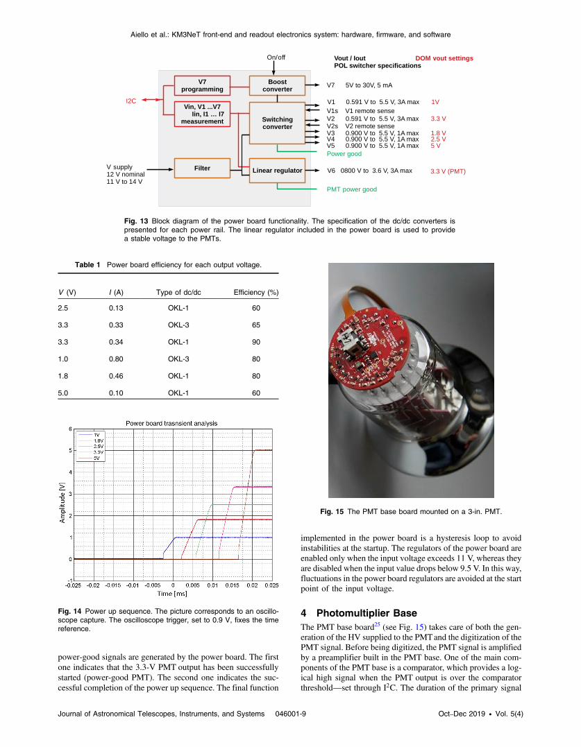
3 Power BoardThe power board,23 shown in Fig. 12, provides power to theCLB and the full DOM. The schematic view of the power boardfunctionality is shown in Fig. 13. The input supply to the powerboard is 12 V. Six regulated voltages (1, 1.8, 2.5, 3.3, 3.3 VPMT, and 5 V) are generated from the 12-V using dc/dc con-verters. The 1, 1.8, 2.5, and 3.3 V outputs are used by the CLBto supply the FPGA. The 3.3-V PMT output supplies the 31PMT base boards and the 5-V voltage is used to supply theacoustic piezo sensor. Moreover, the power board providesanother output, settable via an I2C digital-to-analog converter(DAC), which results in a configurable voltage ranging from0 to 30 V. The settable channel is used by the nanobeacon.The power board uses high-efficiency dc/dc converters in orderto minimize the power consumption in the DOM. The efficien-cies of these dc/dc converters are listed in Table 1.
In order to protect the sensitive electronics inside the DOMfrom the interferences by the high frequency noise produced bythe dc/dc converters, the power board is located in the shieldedpart of the cooling mushroom. The chosen location also pro-vides a better cooling of the power board. The location of thepower board in the DOM is shown in Fig. 2.
3.1 Power Startup
One of the functions of the power board is to provide a propervoltage startup sequence to the FPGA. For this purpose, asequencer has been implemented in the power board in orderto provide the needed sequence of voltages.24 The sequence ofvoltages generated by the power board is shown in Fig. 14. Two
Fig. 11 Content of the serial flash memory. The golden startup imagestarts at address 0, followed by the primary runtime image, and twobackup images. The remainder of the memory contains various typesof persistent states. Fig. 12 The DOM power board, having a diameter of 130 mm.
Fig. 10 Layers and modules of the CLB embedded software.
Journal of Astronomical Telescopes, Instruments, and Systems 046001-8 Oct–Dec 2019 • Vol. 5(4)
Aiello et al.: KM3NeT front-end and readout electronics system: hardware, firmware, and software
power-good signals are generated by the power board. The firstone indicates that the 3.3-V PMT output has been successfullystarted (power-good PMT). The second one indicates the suc-cessful completion of the power up sequence. The final function
implemented in the power board is a hysteresis loop to avoidinstabilities at the startup. The regulators of the power board areenabled only when the input voltage exceeds 11 V, whereas theyare disabled when the input value drops below 9.5 V. In this way,fluctuations in the power board regulators are avoided at the startpoint of the input voltage.
4 Photomultiplier BaseThe PMT base board25 (see Fig. 15) takes care of both the gen-eration of the HV supplied to the PMTand the digitization of thePMT signal. Before being digitized, the PMT signal is amplifiedby a preamplifier built in the PMT base. One of the main com-ponents of the PMT base is a comparator, which provides a log-ical high signal when the PMT output is over the comparatorthreshold—set through I2C. The duration of the primary signal
Fig. 13 Block diagram of the power board functionality. The specification of the dc/dc converters ispresented for each power rail. The linear regulator included in the power board is used to providea stable voltage to the PMTs.
Table 1 Power board efficiency for each output voltage.
V (V) I (A) Type of dc/dc Efficiency (%)
2.5 0.13 OKL-1 60
3.3 0.33 OKL-3 65
3.3 0.34 OKL-1 90
1.0 0.80 OKL-3 80
1.8 0.46 OKL-1 80
5.0 0.10 OKL-1 60
Fig. 14 Power up sequence. The picture corresponds to an oscillo-scope capture. The oscilloscope trigger, set to 0.9 V, fixes the timereference.
Fig. 15 The PMT base board mounted on a 3-in. PMT.
Journal of Astronomical Telescopes, Instruments, and Systems 046001-9 Oct–Dec 2019 • Vol. 5(4)
Aiello et al.: KM3NeT front-end and readout electronics system: hardware, firmware, and software
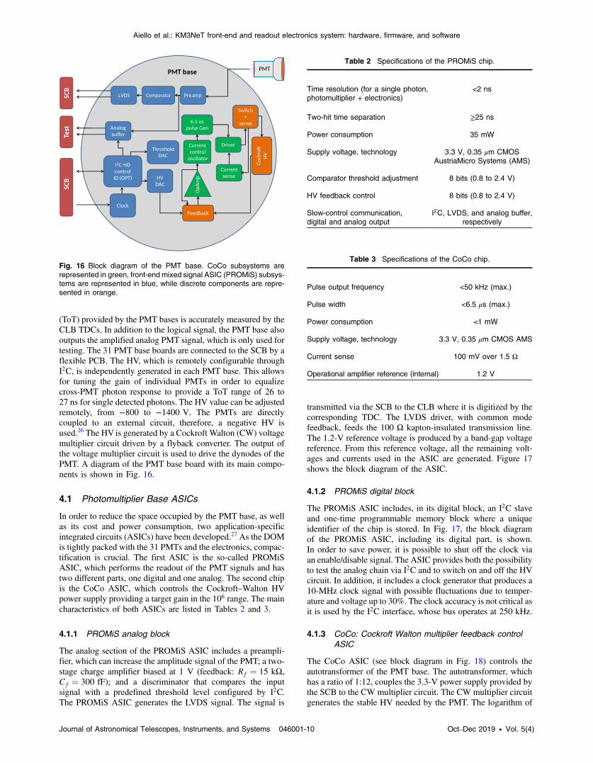
(ToT) provided by the PMT bases is accurately measured by theCLB TDCs. In addition to the logical signal, the PMT base alsooutputs the amplified analog PMT signal, which is only used fortesting. The 31 PMT base boards are connected to the SCB by aflexible PCB. The HV, which is remotely configurable throughI2C, is independently generated in each PMT base. This allowsfor tuning the gain of individual PMTs in order to equalizecross-PMT photon response to provide a ToT range of 26 to27 ns for single detected photons. The HV value can be adjustedremotely, from −800 to −1400 V. The PMTs are directlycoupled to an external circuit, therefore, a negative HV isused.26 The HV is generated by a Cockroft Walton (CW) voltagemultiplier circuit driven by a flyback converter. The output ofthe voltage multiplier circuit is used to drive the dynodes of thePMT. A diagram of the PMT base board with its main compo-nents is shown in Fig. 16.
4.1 Photomultiplier Base ASICs
In order to reduce the space occupied by the PMT base, as wellas its cost and power consumption, two application-specificintegrated circuits (ASICs) have been developed.27 As the DOMis tightly packed with the 31 PMTs and the electronics, compac-tification is crucial. The first ASIC is the so-called PROMiSASIC, which performs the readout of the PMT signals and hastwo different parts, one digital and one analog. The second chipis the CoCo ASIC, which controls the Cockroft–Walton HVpower supply providing a target gain in the 106 range. The maincharacteristics of both ASICs are listed in Tables 2 and 3.
4.1.1 PROMiS analog block
The analog section of the PROMiS ASIC includes a preampli-fier, which can increase the amplitude signal of the PMT; a two-stage charge amplifier biased at 1 V (feedback: Rf ¼ 15 kΩ,Cf ¼ 300 fF); and a discriminator that compares the inputsignal with a predefined threshold level configured by I2C.The PROMiS ASIC generates the LVDS signal. The signal is
transmitted via the SCB to the CLB where it is digitized by thecorresponding TDC. The LVDS driver, with common modefeedback, feeds the 100 Ω kapton-insulated transmission line.The 1.2-V reference voltage is produced by a band-gap voltagereference. From this reference voltage, all the remaining volt-ages and currents used in the ASIC are generated. Figure 17shows the block diagram of the ASIC.
4.1.2 PROMiS digital block
The PROMiS ASIC includes, in its digital block, an I2C slaveand one-time programmable memory block where a uniqueidentifier of the chip is stored. In Fig. 17, the block diagramof the PROMiS ASIC, including its digital part, is shown.In order to save power, it is possible to shut off the clock viaan enable/disable signal. The ASIC provides both the possibilityto test the analog chain via I2C and to switch on and off the HVcircuit. In addition, it includes a clock generator that produces a10-MHz clock signal with possible fluctuations due to temper-ature and voltage up to 30%. The clock accuracy is not critical asit is used by the I2C interface, whose bus operates at 250 kHz.
4.1.3 CoCo: Cockroft Walton multiplier feedback controlASIC
The CoCo ASIC (see block diagram in Fig. 18) controls theautotransformer of the PMT base. The autotransformer, whichhas a ratio of 1:12, couples the 3.3-V power supply provided bythe SCB to the CW multiplier circuit. The CW multiplier circuitgenerates the stable HV needed by the PMT. The logarithm of
Fig. 16 Block diagram of the PMT base. CoCo subsystems arerepresented in green, front-end mixed signal ASIC (PROMiS) subsys-tems are represented in blue, while discrete components are repre-sented in orange.
Table 2 Specifications of the PROMiS chip.
Time resolution (for a single photon,photomultiplier + electronics)
<2 ns
Two-hit time separation ≥25 ns
Power consumption 35 mW
Supply voltage, technology 3.3 V, 0.35 μm CMOSAustriaMicro Systems (AMS)
Comparator threshold adjustment 8 bits (0.8 to 2.4 V)
HV feedback control 8 bits (0.8 to 2.4 V)
Slow-control communication,digital and analog output
I2C, LVDS, and analog buffer,respectively
Table 3 Specifications of the CoCo chip.
Pulse output frequency <50 kHz (max.)
Pulse width <6.5 μs (max.)
Power consumption <1 mW
Supply voltage, technology 3.3 V, 0.35 μm CMOS AMS
Current sense 100 mV over 1.5 Ω
Operational amplifier reference (internal) 1.2 V
Journal of Astronomical Telescopes, Instruments, and Systems 046001-10 Oct–Dec 2019 • Vol. 5(4)
Aiello et al.: KM3NeT front-end and readout electronics system: hardware, firmware, and software

the PMT gain has a linear response to the HV. The ASICreceives feedback from the CW multiplier circuit in order toaccurately control the HV. The control is performed by a seriesof pulses to the switch that is managing the autotransformer.The characteristic pulse width is 6.5 μs and its frequency, whichdetermines the HV, changes according to the HV feedback. TheHV feedback voltage is used for charging (or discharging)a capacitor. The value of the capacitor, loaded by the currentof the HV feedback, sets the frequency. The triangular wavecreated by the charge and discharge of the capacitor is also usedfor generating internal clocks. Another function of the HV feed-back is to avoid the autotransformer saturation in case of shortcircuit.
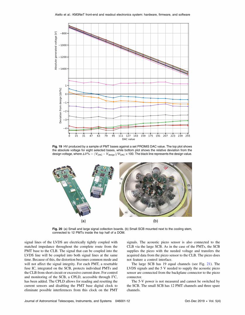
The relation between the PMT DAC value and the actual pro-duced HV is shown in Fig. 19. The relation between the DACvalue and the output voltage can be derived from the PMT baseHV circuit and is given as
EQ-TARGET;temp:intralink-;e001;63;101VHV ¼ −F�Vmin − Vref þD
Vmax − Vmin
255
�þ Vref ; (1)
where D is the DAC value (0 to 255), Vref is the referencevoltage generated by the Cockroft Walton multiplier feedbackcontrol ASIC (1.21 V), Vmin and Vmax are the minimum andmaximum output voltages of the DAC (1.91 and 2.71 V, respec-tively), and F is the feedback path voltage divider factor, whichhas been set to 1000. VHV is the HV generated by the circuit.From this, it follows a range variation of the design outputbetween −698.8 and −1498.8 V for DAC values 0 and 255,respectively. The observed variation among a sample of PMTbases in Fig. 19 is due to resistor tolerances present in the feed-back loop, which total to a maximum of �6%. The nonlinearityand general offset with respect to the design voltage in the plot isdue to the inherent error of the measurement method.
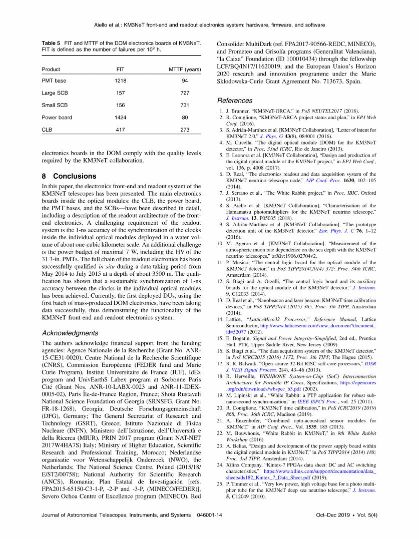
5 Signal Collection BoardThe PMT base-generated LVDS signals are collected on a hubboard, called the SCB. The main function of the SCB is to trans-fer the signals from the PMT base to the TDCs embedded in theCLB. The SCB also transfers the I2C command signals fromthe CLB to the PMT bases in order to monitor and control thePMTs. Each DOM comprises two SCBs, one large and onesmall [Fig. 20(a)]. Figure 20(b) shows one SCB connected tothe PMT bases in half a DOM. The architecture of the SCBconsists of the following parts:
• Backplane connector to the CLB.
• Xilinx Coolrunner complex programmable logic device(CPLD).
• I2C multiplexer.
• Current limit switches.
• PMT channels: 19 in the large SCB and 12 in thesmall SCB.
• One piezo connector (only in the large SCB).
LVDS signaling, as used between the PMT base and theCLB, is less susceptible to cross-talk due to the fact that the two
Fig. 17 Diagram of the PROMiS chip.
Fig. 18 Block diagram of the CoCo chip.
Journal of Astronomical Telescopes, Instruments, and Systems 046001-11 Oct–Dec 2019 • Vol. 5(4)
Aiello et al.: KM3NeT front-end and readout electronics system: hardware, firmware, and software
signal lines of the LVDS are electrically tightly coupled withmatched impedance throughout the complete route from thePMT base to the CLB. The signal that can be coupled into theLVDS line will be coupled into both signal lines at the sametime. Because of this, the distortion becomes common mode andwill not affect the signal integrity. For each PMT, a resettablefuse IC, integrated on the SCB, protects individual PMTs andthe CLB from short circuit or excessive current draw. For controland monitoring of the SCB, a CPLD, accessible through I2C,has been added. The CPLD allows for reading and resetting thecurrent sensors and disabling the PMT base digital clock toeliminate possible interferences from this clock on the PMT
signals. The acoustic piezo sensor is also connected to theCLB via the large SCB. As in the case of the PMTs, the SCBsupplies the piezo with the needed voltage and transfers theacquired data from the piezo sensor to the CLB. The piezo doesnot feature a control interface.
The large SCB has 19 equal channels (see Fig. 21). TheLVDS signals and the 5 V needed to supply the acoustic piezosensor are connected from the backplane connector to the piezoconnector.
The 5-V power is not measured and cannot be switched bythe SCB. The small SCB has 12 PMT channels and three sparechannels.
Fig. 19 HV produced by a sample of PMT bases against a set PROMiS DAC value. The top plot showsthe absolute voltage for eight selected bases, while bottom plot shows the relative deviation from thedesign voltage, whereΔV% ¼ ðVDAC − V designÞ∕VDAC × 100. The black line represents the design value.
Fig. 20 (a) Small and large signal collection boards. (b) Small SCB mounted next to the cooling stem,connected to 12 PMTs inside the top half of a DOM.
Journal of Astronomical Telescopes, Instruments, and Systems 046001-12 Oct–Dec 2019 • Vol. 5(4)
Aiello et al.: KM3NeT front-end and readout electronics system: hardware, firmware, and software

6 DOM Power BreakdownThe power consumption breakdown of the most consumingDOM electronics boards is shown in Table 4. The componentof the DOM with the highest power consumption is the CLB.Inside the CLB, the FPGA and the SFP are the main power con-sumers, followed by the clock conditioner and the nanobeacon.The nanobeacon is only operated when a calibration run isperformed, typically a few minutes once a week.
The SCB consumption is negligible and the 31 PMT basesadd up to a total of 1 W. The power board, mainly because of thedc/dc converter losses, accounts for 10.2% of the total DOM
power consumption. In total, the power consumption of theDOM is around 7 W when fully operational. Keeping the powerdrain low is important both for keeping the overall consumptionof the detector low and minimizing the heat production.
7 ReliabilityMaintenance of DU operated in deep seawater is difficult. Inorder to quantify the reliability of the electronics boards usedin the detector, the FIDES28 method is used. The FIDES meth-odology provides two main engineering tools. The first one con-sists of a handbook for predicting the reliability of the electronicboards analyzed. The second one is a guide to estimate theimpact of the design and manufacturing processes on the reli-ability of the produced boards. FIDES provides a spreadsheettool to calculate the failure in time (FIT) and the mean timeto failure (MTTF) of an electronics board. Given a board, eachof its components is assigned an FIT, which is either provided bythe manufacturer or obtained from the FIDES handbook. Thefinal FIT of a board is the sum of the FITs of each single com-ponent and estimates the failure rate per 109 hours. Once the FITis obtained, it is possible to calculate the probability of failure ina given time as FðtÞ ¼ 1 − RðtÞ, with RðtÞ the probability of asystem to still be operational over a time period t. RðtÞ ¼ e−λt,where λ is the board FIT value and t the time period durationin hours.
The results obtained for the DOM electronics boards are pre-sented in Table 5. To fully quantify the reliability of the boards,it is necessary to evaluate each subsystem included in order toexclude, from the total FIT, those subsystems that are not criticalor do not affect the overall performance of the detector in case offailure. The evaluation is called the failure mode, effects, andcriticality analysis (FMECA). In the case of the power board,FMECA analysis has shown that the failure of the nanobeaconand piezo power supplies has no impact in the overall physicsperformances of the KM3NeT detector, because there is enoughredundancy. Once adjusted, the power board FIT reduces to947. The results obtained by the FIDES method show that the
Fig. 21 Block diagram of the 19 PMT channel interface of the large SCB. The small SCB is analogouswith only 12 channels.
Table 4 DOM measured power breakdown.
Power breakdown
Board Subcomponent Power (W)
Power board 0.72
CLB 4.45
FPGA 2.25
SFP 1.50
Clock conditioner 0.50
Tilt and compass 0.20
Small SCB 0.02
Large SCB 0.02
PMT 31× 1.05
Digital Piezo 0.50
Total power consumption 6.76
Journal of Astronomical Telescopes, Instruments, and Systems 046001-13 Oct–Dec 2019 • Vol. 5(4)
Aiello et al.: KM3NeT front-end and readout electronics system: hardware, firmware, and software
electronics boards in the DOM comply with the quality levelsrequired by the KM3NeT collaboration.
8 ConclusionsIn this paper, the electronics front-end and readout system of theKM3NeT telescopes has been presented. The main electronicsboards inside the optical modules: the CLB, the power board,the PMT bases, and the SCBs—have been described in detail,including a description of the readout architecture of the front-end electronics. A challenging requirement of the readoutsystem is the 1-ns accuracy of the synchronization of the clocksinside the individual optical modules deployed in a water vol-ume of about one-cubic kilometer scale. An additional challengeis the power budget of maximal 7 W, including the HV of the31 3-in. PMTs. The full chain of the readout electronics has beensuccessfully qualified in situ during a data-taking period fromMay 2014 to July 2015 at a depth of about 3500 m. The quali-fication has shown that a sustainable synchronization of 1-nsaccuracy between the clocks in the individual optical moduleshas been achieved. Currently, the first deployed DUs, using thefirst batch of mass-produced DOM electronics, have been takingdata successfully, thus demonstrating the functionality of theKM3NeT front-end and readout electronics system.
AcknowledgmentsThe authors acknowledge financial support from the fundingagencies: Agence Nationale de la Recherche (Grant No. ANR-15-CE31-0020), Centre National de la Recherche Scientifique(CNRS), Commission Européenne (FEDER fund and MarieCurie Program), Institut Universitaire de France (IUF), IdExprogram and UnivEarthS Labex program at Sorbonne ParisCité (Grant Nos. ANR-10-LABX-0023 and ANR-11-IDEX-0005-02), Paris Île-de-France Region, France; Shota RustaveliNational Science Foundation of Georgia (SRNSFG, Grant No.FR-18-1268), Georgia; Deutsche Forschungsgemeinschaft(DFG), Germany; The General Secretariat of Research andTechnology (GSRT), Greece; Istituto Nazionale di FisicaNucleare (INFN), Ministero dell’Istruzione, dell’Università edella Ricerca (MIUR), PRIN 2017 program (Grant NAT-NET2017W4HA7S) Italy; Ministry of Higher Education, ScientificResearch and Professional Training, Morocco; Nederlandseorganisatie voor Wetenschappelijk Onderzoek (NWO), theNetherlands; The National Science Centre, Poland (2015/18/E/ST2/00758); National Authority for Scientific Research(ANCS), Romania; Plan Estatal de Investigación [refs.FPA2015-65150-C3-1-P, -2-P and -3-P, (MINECO/FEDER)],Severo Ochoa Centre of Excellence program (MINECO), Red
Consolider MultiDark (ref. FPA2017-90566-REDC, MINECO),and Prometeo and Grisolía programs (Generalitat Valenciana),“la Caixa” Foundation (ID 100010434) through the fellowshipLCF/BQ/IN17/11620019, and the European Union’s Horizon2020 research and innovation programme under the MarieSkłodowska-Curie Grant Agreement No. 713673, Spain.
References1. J. Brunner, “KM3NeT-ORCA,” in PoS NEUTEL2017 (2018).2. R. Coniglione, “KM3NeT-ARCA project status and plan,” in EPJ Web
Conf. (2016).3. S. Adrián-Martínez et al. [KM3NeT Collaboration], “Letter of intent for
KM3NeT 2.0,” J. Phys. G 43(8), 084001 (2016).4. M. Circella, “The digital optical module (DOM) for the KM3NeT
detector,” in Proc. 33nd ICRC, Rio de Janeiro (2013).5. E. Leonora et al. [KM3NeT Collaboration], “Design and production of
the digital optical module of the KM3NeT project,” in EPJ Web Conf.,vol. 136, p. 4008 (2017).
6. D. Real, “The electronics readout and data acquisition system of theKM3NeT neutrino telescope node,” AIP Conf. Proc. 1630, 102–105(2014).
7. J. Serrano et al., “The White Rabbit project,” in Proc. IBIC, Oxford(2013).
8. S. Aiello et al. [KM3NeT Collaboration], “Characterisation of theHamamatsu photomultipliers for the KM3NeT neutrino telescope,”J. Instrum. 13, P05035 (2018).
9. S. Adrián-Martínez et al. [KM3NeT Collaboration], “The prototypedetection unit of the KM3NeT detector,” Eur. Phys. J. C 76, 1–12(2016).
10. M. Ageron et al. [KM3NeT Collaboration], “Measurement of theatmospheric muon rate dependence on the sea depth with the KM3NeTneutrino telescopes,” arXiv:1906.02704v2.
11. P. Musico, “The central logic board for the optical module of theKM3NeT detector,” in PoS TIPP2014(2014) 372; Proc. 34th ICRC,Amsterdam (2014).
12. S. Biagi and A. Orzelli, “The central logic board and its auxiliaryboards for the optical module of the KM3NeT detector,” J. Instrum.9, C12033 (2014).
13. D. Real et al., “Nanobeacon and laser beacon: KM3NeT time calibrationdevices,” in PoS TIPP2014 (2015) 365, Proc. 3th TIPP, Amsterdam(2014).
14. Lattice, “LatticeMico32 Processor,” Reference Manual, LatticeSemiconductor, http://www.latticesemi.com/view_document?document_id=52077 (2012).
15. E. Bogatin, Signal and Power Integrity–Simplified, 2nd ed., PrenticeHall, PTR, Upper Saddle River, New Jersey (2009).
16. S. Biagi et al., “The data acquisition system of the KM3NeT detector,”in PoS ICRC2015 (2016) 1172, Proc. 3th TIPP, The Hague (2015).
17. R. R. Balwaik, “Open-source 32-Bit RISC soft-core processors,” IOSRJ. VLSI Signal Process. 2(4), 43–46 (2013).
18. R. Herveille, WISHBONE System-on-Chip (SoC) InterconnectionArchitecture for Portable IP Cores, Specifications, https://opencores.org/cdn/downloads/wbspec_b3.pdf (2002).
19. M. Lipinski et al., “White Rabbit: a PTP application for robust sub-nanosecond synchronization,” in IEEE ISPCS Proc., vol. 25 (2011).
20. R. Coniglione, “KM3NeT time calibration,” in PoS ICRC2019 (2019)868, Proc. 36th ICRC, Madison (2019).
21. A. Enzenhofer, “Combined opto-acoustical sensor modules forKM3NeT,” in AIP Conf. Proc., Vol. 1535, 185 (2013).
22. M. Bouwhouis, “White Rabbit in KM3NeT,” in 9th White RabbitWorkshop (2016).
23. A. Belias, “Design and development of the power supply board withinthe digital optical module in KM3NeT,” in PoS TIPP2014 (2014) 188;Proc. 3rd TIPP, Amsterdam (2014).
24. Xilinx Company, “Kintex-7 FPGAs data sheet: DC and AC switchingcharacteristics,” https://www.xilinx.com/support/documentation/data_sheets/ds182_Kintex_7_Data_Sheet.pdf (2019).
25. P. Timmer et al., “Very low power, high voltage base for a photo multi-plier tube for the KM3NeT deep sea neutrino telescope,” J. Instrum.5, C12049 (2010).
Table 5 FIT and MTTF of the DOM electronics boards of KM3NeT.FIT is defined as the number of failures per 109 h.
Product FIT MTTF (years)
PMT base 1218 94
Large SCB 157 727
Small SCB 156 731
Power board 1424 80
CLB 417 273
Journal of Astronomical Telescopes, Instruments, and Systems 046001-14 Oct–Dec 2019 • Vol. 5(4)
Aiello et al.: KM3NeT front-end and readout electronics system: hardware, firmware, and software

26. S. Adrián-Martínez et al., “A method to stabilise the performance ofnegatively fed KM3NeT photomultipliers,” J. Instrum. 11, P12014(2016).
27. D. Gajanana et al., “ASIC design in the KM3NeT detector,” J. Instrum.8, C02030 (2013).
28. P. Pougnet et al., “Reliability prediction of embedded electronicsystems: the FIDES guide,” in Embedded Mechatron. Syst., pp. 185–211 (2015).
Vincent van Beveren is a PhD candidate and embedded softwareengineer at the National Institute for Subatomic Physics Nikhef.He received his BS degree in computer science and informationtechnology from the Hogeschool Utrecht in 2004. He has collaboratedon multiple publications on various topics. His areas of expertise areultralower power embedded systems, digital signal processing, andinternet of things.
David Calvo is a PhD candidate and research engineer at theInstituto de Física Corpuscular of Valencia. He received his MS
degree in computing from the University Jaume I in 2006, his MSdegree in electronics from the University of Valencia in 2009, andhis MS degree in electronic systems design from the PolytechnicUniversity of Valencia in 2012. His research interests are focused ondigital electronics, synchronization, and readout acquisition systems.He is the author of several publications on electronics.
Diego Real is a PhD candidate and research engineer at the Institutode Física Corpuscular. He received his BS degree in electronics in1996 and his MS degree in control and electronics in 2000, both fromthe Polytechnic University of Valencia. He is the author of severalpublications on electronics. His current research interests includeacquisition and synchronization systems for particle physics. He hasbeen the electronics project leader of the KM3NeT telescope and amember of the technical advisory board of the GVD-Baikal telescopesince 2013.
Biographies of the other authors are not available.
Journal of Astronomical Telescopes, Instruments, and Systems 046001-15 Oct–Dec 2019 • Vol. 5(4)
Aiello et al.: KM3NeT front-end and readout electronics system: hardware, firmware, and software
View publication statsView publication stats