KJ 8056 CHAPTER 1. ELECTROCHEMICAL SENSORS … 3056/Teaching mat/ISFET_slides.pdf · CHAPTER 1....
13
Created by F. G. Banica Created on 9/7/2006 8:27 AM NTNU-Dept. of Chemistry KJ 8056 CHAPTER 1. ELECTROCHEMICAL SENSORS Part B. Semiconductor devices as chemical sensors By F. G. Banica, August 2006 CONTENTS B.1. Semiconductors devices a) Silicon and Germanium semiconductors b) Semiconductor diodes c) Field effect transistors (FET) B.2. Ion-selective field-effect transistors (ISFET) a) pH-sensitive sensors (pH-ISFET) b) Polymer membranes for ISFET c) Heterogeneous membranes d) Multiple function ISFET e) Reference FET B.3. Gas sensitive FET B.4. Enzyme-based FET sensors B.5. Electronic devices for the operation of the FET chemical sensor. INTRODUCTION Semiconductor devices (like diodes and transistors) are essential components of any kind of electronic equipment. Such device allows controlling the current flow in electric circuits in order to do information convey and processing. An ion sensing layer can be combined with a semiconductor device. The electric charge which develops at the solution interface (FRAME 1) will exert an effect on the electric properties of that device. This is the underlying principle of the semiconductor-based ion sensors. The recognition principles and methods are mostly alike to that encountered with the membrane ion sensors (Chapter 1, Part A). The semiconductor device itself plays the role of the transduction part. The present Part of Chapter 1 starts up with a presentation of semiconductor materials and semiconductor devices. Further, various applications of such devices in sensor science and technology are presented.
Transcript of KJ 8056 CHAPTER 1. ELECTROCHEMICAL SENSORS … 3056/Teaching mat/ISFET_slides.pdf · CHAPTER 1....

Created by F. G. Banica Created on 9/7/2006 8:27 AM
NTNU-Dept. of Chemistry
KJ 8056
CHAPTER 1. ELECTROCHEMICAL SENSORS
Part B. Semiconductor devices as chemical sensors
By F. G. Banica, August 2006
CONTENTS
B.1. Semiconductors devices
a) Silicon and Germanium semiconductors
b) Semiconductor diodes
c) Field effect transistors (FET)
B.2. Ion-selective field-effect transistors (ISFET)
a) pH-sensitive sensors (pH-ISFET)
b) Polymer membranes for ISFET
c) Heterogeneous membranes
d) Multiple function ISFET
e) Reference FET
B.3. Gas sensitive FET
B.4. Enzyme-based FET sensors
B.5. Electronic devices for the operation of the FET chemical sensor.
INTRODUCTION
Semiconductor devices (like diodes and transistors) are essential components of any kind of electronic equipment. Such device allows controlling the current flow in electric circuits in order to do information convey and processing. An ion sensing layer can be combined with a semiconductor device. The electric charge which develops at the solution interface (FRAME 1) will exert an effect on the electric properties of that device. This is the underlying principle of the semiconductor-based ion sensors. The recognition principles and methods are mostly alike to that encountered with the membrane ion sensors (Chapter 1, Part A). The semiconductor device itself plays the role of the transduction part. The present Part of Chapter 1 starts up with a presentation of semiconductor materials and semiconductor devices. Further, various applications of such devices in sensor science and technology are presented.

Created by F. G. Banica Created on 9/7/2006 8:27 AM
FRAME 1
ION SENSORS
The solution /membrane interface
Charge distribution
Solution
Ion Exchanger
H+Si- O-
An ion transfer process occurs at the membrane-solution interface (e.g. positive ions
from the solution are bound to the negative receptor sites at the membrane surface).
Consequently, a non-uniform charge distribution develops, with an excess positive
charge in the solution phase.
The excess charge can provide information about the ion concentration in the solution
if a suitable method for charge assessment is available.
Assessment of the interface electrical charge can be done by:
• Potentiometry (using membrane sensors, Chapter 1, part A), or
• Electrostatic effects using semiconductor device (Chapter 1, part B)

Created by F. G. Banica Created on 9/7/2006 8:27 AM
FRAME 2 SEMICONDUCTOR DEVICES
The doping of semiconductors
Semiconductor devices (diodes, transistors...) are based on doped silicon materials. Doping consists of adding a very small percentage of foreign atoms in the regular crystal lattice of silicon. It produces dramatic changes in its electrical properties.
Impurity atoms with 5 valence electrons produce n-type semiconductors by contributing extra electrons. Impurity atoms with 3 valence electrons produce p-type semiconductors by producing a “hole” or electron vacancy (i.e. a positively charged site). In each case, the electric conductivity of the semiconductor increases very much. Electricity transport is done by free electrons movement in n-type semiconductors and by holes drift in the p-type semiconductors.

Created by F. G. Banica Created on 9/7/2006 8:27 AM
FRAME 3
SEMICONDUCTOR DEVICES
The Semiconductor Diode
-Forward biasing - I ≠ 0
n p
+-
I
-Reverse biasing -
I = 0
pnI = 0
+ -

Created by F. G. Banica Created on 9/7/2006 8:27 AM
FRAME 4
SEMICONDUCTOR DEVICES
The Field Effect Transistor (FET)
Oxide Insulator (SiO 2 )
S
U G
Dp
nn
G
U D
I D
I=0
+ + + +- - - - - - -
+
+
-
-
Metallayer (gate)
Semiconductor
S = Source D = Drain G = Gate
A FET consists of a small piece of p-type silicon with two n-type regions called
source and drain. The surface is covered by an insulating layer (SiO2) and a thin metal layer
is deposited above to for the gate. No current can flow betwen the source and the drain
because a reverse biasing occurs at one of the p-n junction (FRAME 3). However, if a
positive electric charge is loadet to the gate (by means f the UG voltage source), free electron
may appear between the source and the drain, immediately under the gate/insulator makeup.
Thus, an inversion layer appears. In this region (also called channel) the p-type
semiconductor is converted into a n-type and no reverse biasing occurs any longer. A current
(ID) can flow between the source and the drain in this instance.
ID depends on the free electron density in the channel, which is dictated by UG. It
depends also on electron velocity, which is a function of the source-drain voltage , UD. Small
changes in UG result in large modifications of ID. Therefore, the current flowing through the
FET can be controlled by the gate voltage. See FRAME 5 for details.

Created by F. G. Banica Created on 9/7/2006 8:27 AM
FRAME 5 Current flow through the FET: the ID - UG relation
Current starts to flow between source and drain when the channel begins to form. This occurs when the gate voltage UG rises above a critical value (threshold voltage, UT, Fig. 1).
VG
ID
VT U T U G
Fig. 1. UD is the voltage between source and drain; UG is the voltage applied to the gate; ID is the
current flowing between source and drain.
The gate/insulator/substrate assembly behaves as a capacitor with a capacitance CG. It stores a channel charge Q given by : (1) ( )G G TQ C U U= −
The drain current represents the amount of electric charge that passes across the channel per time unit: (2) /DI Q t= Where:
(3) channel length Lt
electron velocity v= =
and:
(4) ( )x
( / )D
v electron mobility(strength of the electric field)= U Lµ
=
So: (5) 2
Dt L Uµ= Finally:
(6) 2 ( )GD D G T
CI U U ULµ= −
Equation (6) holds at low UG values, when the potential along the channel is approximately constant. It shows that at a constant UG, ID is
proportional to UD. Also, at a constant UD, ID is proportional to UG. This conclusion is very important to FET applications in sensor devices. At high UG values, the ID –UD relation is more complicated than the linear relationship (6) (see Fig. 2).
U D ,V
U G ,V
ID, m
A
0 2010
1
2
3
1
2
3
4
Fig. 2 .

Created by F. G. Banica Created on 9/7/2006 8:27 AM
FRAME 6 FET based pH sensors (pH ISFET)
Structure and principles
S
U G
D p
n n
U D
i D
i G =0
Solution
Reference electrode
-+
+- H + selective
solid layer
B
p Type Semiconductor
In order to build up a pH sensitive FET, the insulator layer should be replaced by a H+ binding material (e.g, a –SiO- containing material). This one is in contact with the sample solution and a reference electrode assumes the role of the gate. A potential difference develops at the solution interface as a result of ion transfer (FRAME 1):
(7) ' 2.303 log ' 2.303i H
RT RTE k s a k s pHzF zF+= + = −
k’ is a constant and s is the sensitivity factor (s = 0.95 - 1.00)
The interface potential difference adds to UG and influences the drain current (ID )which becomes pH-dependent (FRAME 5, eqn. (6)). This forms the basis for pH determination by means of the FET senssor. The picture to the left displays a miniature pH ISFET. Miniaturization is the main advantage of the FET sensors (see also FRAME 10).

Created by F. G. Banica Created on 9/7/2006 8:27 AM
FRAME 7
The pH ISFET
Operation at constant ID
I D
U G
pH 2 < pH 1
I D = const
U(pH 2 )U(pH 1 )
Eqn. (7) along with eqn. (6) suggest that the drain current is a pH function and can be employed as analytical signal for pH determination at a constant gate voltage. However, for practical reasons it is more suitable to operate the sensor at a constant ID. The Figure above demonstrates the shift of the ID- UG curve when the pH changes from pH1 to pH2. An automatic devices adjusts UG so as to keep ID constant. The increment in UG ( 1 2( ) ( )GU U pH U pH∆ = − compensates the contribution of the interface potential (Ei, FRAME 6) i.e.
G iU E−∆ = Therefore, GU−∆ is a linear function of pH and a linear calibration function ( vs. GU pH∆ ) is the basis for sensor calibration.

Created by F. G. Banica Created on 9/7/2006 8:27 AM
FRAME 8
The pH ISFET: Several versions
STANDARD
PLAT
CONIC
LANCE
The pH ISFET: figures of merit
• Sensitivity: 56 - 58 mV
• pH range: 0 -14
• No glass
• Robust
• Fast response
• Easy manipulation
• Can be stored in dry state
• Easy cleaning (tooth brush + soap!)
• The shape can be adapted for various applications
pH ISFET sensors are commercially available
Standard Conical
Flat Lance

Created by F. G. Banica Created on 9/7/2006 8:27 AM
FRAME 9
The Ion Selective FET Sensor
( ISFET )
S
U G
D p
n n
U D
I D
I G=0Solution
Reference electrode
-+
+-
Ion-selectivelayer
Insulator (SiO2)
B
p-type semiconductor
The ion selective layer (which forms the sensing part) consists of a plastic
(PVC) membrane which includes an ion receptor. The receptor can be either a
liquid ion exchanger or a neutral macrocyclic ligand. Measuring principles are
similar to that presented for the pH ISFET (FRAME 7 and FRAME 1).

Created by F. G. Banica Created on 9/7/2006 8:27 AM
FRAME 10
ISFET as a flow direction and flow rate transducer
Reactie anodicaReactie catodica
The generator electrode (Pt) produces H+ ion by water electrolysis (the cathode is not shown). The pH sensors indicate the fluid flow direction and speed by means of pH difference between the test points.
ISFET –Miniature Multiple Sensor
Reference
Flow direct.
Flow rate
Temperature
pH
Penicillin
Various chemical and physical parameters can be measured by the above multiple sensor which was designed for monitoring penicillin fabrication.
Anodic reaction (Pt):2H2O → 4H+ + 4e- + O2
Cathodic reaction: 2 H2O + 2e- → 2OH- + H2

Created by F. G. Banica Created on 9/7/2006 8:27 AM
FRAME 11
Schematics of an ISFET measuring principles As a result of ion exchange at the sensor-solution interface, an interface membrane Ei develops ((FRAME 7 and FRAME 1). In order to keep ID constant, UG is automatically adjusted to ( )G GU U+∆ . As GU∆ = -Ei , it depends on the ion concentration according to a logarithm low (Donnan potential, see Chapter 1, part A). Therefore, GU∆ provides the expected analytical information.
U D =const U G (adjustable)
Reference Electrode
ISFET
Sample
I D =const
In the Fig. above, the sensing device (left-down) is oversized for the sake of clarity
Created by F. G. Banica Created on 9/7/2006 8:27 AM
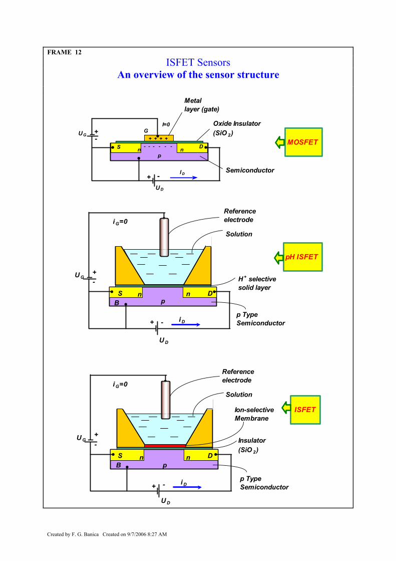
FRAME 12
ISFET Sensors An overview of the sensor structure
S
U G
D p
n n
U D
i D
i G=0
Solution
Reference electrode
-+
+- H + selective
solid layer
B
p Type Semiconductor
Oxide Insulator (SiO 2)
S
UG
D p
n n
G
U D
I D
I=0
+ + + +- - - - - -
+
+
-
-
S
U G
D p
n n
U D
i D
i G=0Solution
Reference electrode
-+
+-
Ion-selectiveMembrane
Insulator (SiO 2)
B
p Type Semiconductor
Metallayer (gate)
Semiconductor
MOSFET
pH ISFET
ISFET