KG11-A exclusive-OR and CRC block check manualbitsavers.informatik.uni-stuttgart.de/ · It contains...
72
KG11-A exclusive-OR and CRC block check manual
Transcript of KG11-A exclusive-OR and CRC block check manualbitsavers.informatik.uni-stuttgart.de/ · It contains...

KG11-A exclusive-OR and CRC block check manual


(
(~
KG11-A exclusive-OR and CRC block check manual
DEC-II-HKGAA-B-D
digital equipment corporation • maynard. massachus~tts

I st Edition, May 1972 2nd Printing (Rev), October 1972 3rd Printing, February 1973 4th Printing, July 1973 5th Printing, October 1974
Copyright © 1972, 1973, 1974 by Digital Equipment Corporation
The material in this manual is for informational purposes and is subject to change without notice.
Printed in U.S.A.
The following are trademarks of Digital Equipment
Corporation, Maynard, Massachusetts:
DEC FLIP CHIP DIGITAL UNIBUS
PDP FOCAL COMPUTER LAB
.,

- --~--------- - ------------------------------
( CONTENTS
Page
CHAPTER 1 INTRODUCfION
CHAPTER 2 GENERAL DESCRIPTION
2.1 Introduction 2-1
2.2 Functional Description 2-1
2.2.1 System Description 2-1
2.2.2 KG 11-A Functional Units 2-2 <' 2.3 Overall Functional Operation 2-4
2.3.1 Normal Cycle Operation 24
2.3.2 Single-Step Operation 2-4
2.4 Physical Description 2-5
CHAPTER 3 DETAILED DESCRIPTION
3.1 Introduction 3-1
3.2 Address Selector and Gating Control 3-1
3.2.1 Address Assignments 3-1
3.2.2 Address Selector and Gating Control 3-2
3.2.3 Gating Control Logic 3-4
3.3 Control and Status Register ,3,6,
C~ 3.4 Data Register 3-6
3.5 Block Check Character (BCC) Register 3-9
3.6 Control Signals Generated by the CSR 3-10
3.6.l Introduction 3-10
3.6.2 Mode Selection Bits D02:00 and DDB Bit D03 3-10
3.6.3 CLEAR Bit D04 3-11
3.6.4 STEP Bit DOS and Shift Enable (SEN) Bit D06 3-12
3.6.5 Shift Clock and Shift Control Logic 3-14
3.66 Exc1usive-OR Operators and Feedback Logic 3-17
CHAPTER 4 PROGRAMMING INFORMATION
4.1 Introduction 4-1
4.2 LRC and CRC Codes 4-1
4.2.1 Introduction 4-1
4.2.2 CRC-16 4-1
4.2.3 CRC-12 4-2
4.2.4 CRC-CCITT 4-2
4.2.5 LRC-8 4-2
4.2.6 LRC-16 4-2
4.3 Recommended Programming PraCtices 4-3
4.3.l Introduction 4-3
4.3.2 BCC Computation on a Message Basis 4-3
l 4.3.3 Partial BCC Computation (Character-by-Character) 4-5
iii
CONTENTS (Cont) ( Page
4.3.4 Single-Step Operation 4-5
CHAPTERS MAINTENANCE
5.1 Introduction 5-1
5.2 Testing and Diagnostics 5-1
5.3 Test Points 5-1
APPENDIX A BCC COMPUTATION FOR LRC AND CRC
A.l Introduction A-I
A.2 Longitudinal Redundancy Checking A-I
A.3 Cyclic Redundancy Checking A-I
A.3.1 Introduction A-I
A.3.2 Mathematical Background A-2
A.3.3 Hardware Implementation of CRC A-4
AA Hardware Configuration of BCC Register A-5
APPENDIXB ABBREVIATIONS
APPENDIXC INTEGRA TED CIRCUIT DESCRIPTIONS
C 7474 Dual D-Type Edge-Triggered Flip-Flops C-3
8242 4-Bit Digital Comparator (Quad Exclusive-NOR) C-5
8266 2-Input 4-Bit Digital Multiplexer C-7
8271 4-Bit Shift Register C-9
74197 Presettable Binary Counter/Latch C-ll
ILLUSTRATIONS
Figure No. Title Page
2-1 Typical System, Block Diagram 2-2
2-2 KG11-A X-OR and CRC Block Check Option, Block Diagram 2-2
3-1 KG ll-A Address Word for Data Register 3-1
3-2 Typical Jumper Connections in Address Decoder, Logic Diagram 3-3
3-3 Address Selection Logic and Gating Control Logic, Block Diagram 3-5
3-4 Control Signals Generated During DATI (Read) Operation,
Logic Diagram 3-5
3-5 Control Signals Generated During DATO (Write) Operation,
Logic Diagram 3-6
3-6 Control and Status Read/Write Functions, Logic Diagram 3-7
3-7 Control and Status Register Bit Assignments 3-7
3-8 Data Register Format 3-9
3-9 BCC Register Format 3-9 l iv

( ILLUSTRATIONS (Cont)
Figure No. Title Page
3-10 Mode Selection Control Signals; Logic Diagram HI
3-11 Clear and Initialize Control Signals, Logic Diagram 3-12
3-12 STEP and SEN Control Signals, Logic Diagram 3-13
3-13 Shift Clock and Shift Control, Logic Diagram 3-15
3-14 Counter States and Overflow for Eight Shift Pulses 3-17
3-15 Counter States and Overflow for 16 Shift Pulses 3-18
3-16 Control of 8266 Multiplexer in Feedback Circuit, Logic Diagram 3-19
4-1 BCC Computation on a Message Basis, Flow Chart 4-3
4-2 Step Mode Operation, Flow Chart 4-6
A-I BCC Computation for Four 8-Bit Characters Using LRC-8 A-2
A-2 BCC Computation Using Long Division Method With CRC-16
as Generator A-4
A-3 BCC Accumulation Using CRC-12, Transmit Sequence A-6
A-4 BCC Accumulation Using CRC-CCITT, Transmit Sequence A-7
A-5 BCC Accumulation Using CRC-16, Transmit Sequence A-8
A-6 BCC Accumulation Using CRC-16, Receive Sequence A-9
A-7 BCC Register, Block Diagram A-lO
TABLES
C Table No. Title Page
3-1 KG 11-A Gating Signals 3-2
3-2 KG 11-A Select Signals 3-4
3-3 Control and Status Register Bit Functions 3-8
5-1 KG11-A Test Points 5-2
v


CHAPTER 1
INTRODUCTION
The KG Il-A Exclusive-OR and CRC Block Check Option provides error detection capabilities for data communi
cation applications. It is used primarily to compute the block check character (BCC) that appears at the end of a
block of data transmitted over a serial synchronous line. The KG Il-A operates, non-concurrently, with any
number of devices.
Although signals are transferred between the KG II-A and the Unibus, this manual does not describe the operation
of the Unibus. A detailed description of the Unibus is presented in the PDP-I} Unibus Interface Manual,
DEC-II-HIAB-D.
The manual provides the user with the theory of operation necessary to understand and maintain the KG II-A
Exclusive-OR and CRC Block Check Option. The level of discussion assumes that the reader is familiar with basic
digital computer theory.
This manual is organized into five chapters: Introduction, General Description, Detailed Description, Program
ming Information, and Maintenance. An appendix is included that describes various BCC accumulations in
graphic form. A separate set of engineering logic drawings is provided with each KG I I-A and is identified as
D-CS-M72SI-Q-I, sheets 1 through 4.
1-1

(
.,'
c
l
2.1 INTRODUCTION
CHAPTER 2
GENERAL DESCRIPTION
This chapter presents an overview of the operation of the KG ll-A Exclusive-OR and CRC Block Check Option.
It contains a functional description that is keyed to the block diagram level. In addition, the discussion includes
some background information on longitudinal and cyclic redundancy checking.
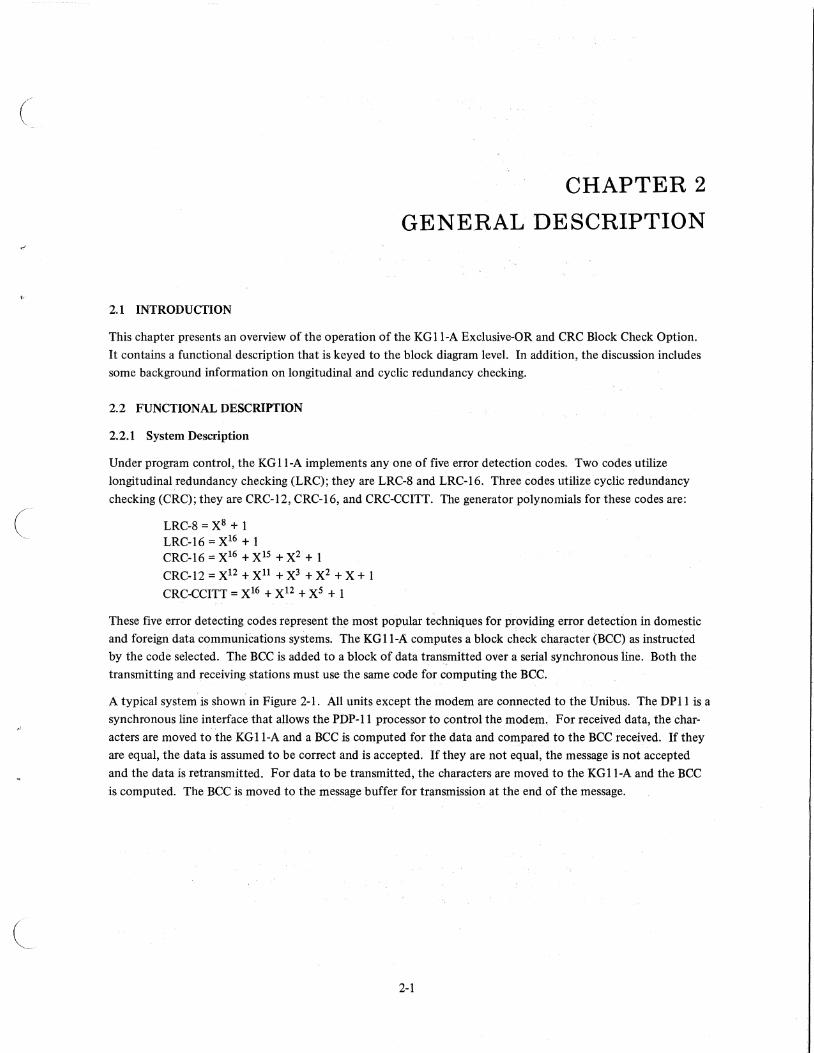
2.2 FUNCTIONAL DESCRIPTION
2.2.1 System Description
Under program control, the KG ll-A implements anyone of five error detection codes. Two codes utilize
longitudinal redundancy checking (LRC); they are LRC-8 and LRC-I6. Three codes utilize cyclic redundancy
checking (CRC); they are CRC-12, CRC-16, and CRC-CCITT. The generator polynomials for these codes are:
LRC-8 = X8 + 1 LRC-I6 = XI6 + 1 CRC-16 = X I6 + XIS + X2 + 1
CRC-12 = X12 + Xll + X 3 + X2 + X + 1
CRC-CCITT = XI6 + X12 + x5 + 1
These five error detecting codes represent the most popular techniques for providing error detection in domestic
and foreign data communications systems. The KG ll-A computes a block check character (BCC) as instructed
by the code selected. The BCC is added to a block of data transmitted over a serial synchronous line. Both the
transmitting and receiving stations must use the same code for computing the BCC.
A typical system is shown in Figure 2-1. All units except the modem are connected to the Unibus. The DPII is a
synchronous line interface that allows the PDP-II processor to control the modem. For received data, the char
acters are moved to the KG 11-A and a BCC is computed for the data and compared to the BCC received. If they
are equal, the data is assumed to be correct and is accepted. If they are not equal, the message is not accepted
and the data is retransmitted. For data to be transmitted, the characters are moved to the KG II-A and the BCC
is computed. The BCC is moved to the message buffer for transmission at the end of the message.
2-1

t-- TO REMOTE STATION
II-OB73
Figure 2-1 Typical System, Block Diagram
2.2.2 KGll-A Functional Units
The major functional units of the KG 1 I-A include the following (Figure 2-2):
a. address selector b. gating control logic c. Unibus receivers and drivers d. control and status register (CSR) e. data register f. BCC register g. shift clock and shift control logic h. exclusive-OR and feedback logic
A<17:00> ClK C<OI:OO>
U MSYN SSYN
N I B 0<15:00> U 5
ClK UNIBUS
0<15:06> DRIVERS
II-Q874
Figure 2-2 KGII-A X-OR and CRC Block Check Option, Block Diagram
. . " ~ .
a. Address Selector - The information on the Unibus address lin~--{17:00> and control lines C (01 :00> is decoded by the address selector. It provides select and gating signals that determine which unit (CSR, data register, or BCC register) has been selected and whether it is to perform an input or output transaction. The logic is equivalent to the standard Address Selector Module MIOS.
(continued on next page)
2-2
(
C
( '----
b.
c.
d.
Gating Control Logic - The gating control logic uses the address selector outputs to provide input/ output signal access for the CSR, data register, and BCC register. It generates enabling signals to read and write the CSR, load the data register, and read the BCC register.
Unibus Receivers and Drivers - Buffer all signals to and from the Unibus and the KG II-A.
Control and Status Register - The 9-bit CSR controls the operation oftheKGll-A: It selects the mode of operation and the polynomial (code) to be used. The control functions require five bits that are read/write and two that are write-only. Two bits are read-only.
A list of the bits is shown below.
Bit Type Signal Function
02:00 read/write 16 BCC (00) Mode selection bits. Determines the poly-LRC (01) nomial (code) to generate the BCC. CRC I!C (02)
03 read/write double data Determines whether one or two characters byte (DDB) (16 bits maximum) are loaded into the
data register.
04 write-only clear (CLR) Clears the BCC register.
05 write-only STEP Enables the single-step mode of opera-tion which is used for diagnostic purposes. Used in conjunction with bit 06 (SEN).
06 read/write shift-enable Determines the KG 1 I-A mode of opera-(SEN) tion: cycle or normal mode; and step or
diagnostic mode.
07 read-only DONE Controls the mode of operation (parallel load or shift) of the data register. Also controls the shift clock.
08 read-only quotient (QUO) Result of the exclusive-OR of the LSB of the data register and the LSB of the BCC register. Used for diagnostic; purposes during the step mode.
15:09 not used
e: Data Register - The data register is a16-bit write-only register. It is the input register for the data on which the BCC is computed. Load is accomplished in parallel from the Unibus data lines. The data register is operated in a serial, shift right mode to enter data into the BCC register during computation of the BCC.
f. BCC Register - The BCC register is a l6-bit read-only register that maintains the BCC accumulation.
g. Shift Clock and Shift Control Logic - The shift clock provides the pulses to shift the data register and the BeC register during a BCC accumulation. The shift control logic provides the required number of shift pulses to these registers in accordance with the polynomial selected.
h. Exclusive-OR and Feedback Logic - This logic sets up the correct number of exclusive-OR operators and feedback paths for the BCC register in accordance with the polynomial selected.
2-3

2.3 OVERALL FUNCTIONAL OPERATION
2.3.1 Normal Cycle Operation
The KG ll-A can be used to compute a BCC in two ways: on a message basis or on a character-by-character basis.
It is recommended that the KG II-A be used to compute the BCC on a message basis. This discussion assumes a
message BCC computation; details of a character-by-character (partial) BCC computation are covered in Chapter 4,
Programming Information.
The first step in operating the KG II-A is the initializing process. The program moves a command word to the
CSR by placing the CSR address (7707XO) on address lines A 07:00> and selecting control lines CO I = 0 and
COO = I, which provide a DATO (write) bus data transfer. The signals are sent to the address selection logic which
decodes them and asserts SELECf 0 H and OUT LOW H. These signals are sent to the gating control logic to
enable a write operation for the CSR which strobes the information on data lines D <06:00> into the CSR. The
data lines were selected by the program simultaneously with the A and C lines and are the control bits for the
CSR. They perform the following functions:
a. Bits 16BCC (DOO), LRC (DOl), and CRC IIC (D02) select the polynomial to be used in computing the BCC. They provide the correct exclusive-OR operator and feedback configuration for the BCC register in accordance with the polynomial selected. LRC and 16BCC also preset the shift counter to 0 or 2, as required, to generate the correct number of pulses (8 or 6 pulses if DDB = 0; 16 or 12 if DDB = 1).
b. Bit DDB (D03) determines whether one or two characters are to be loaded into the data register. When DDB = I, the number of shift pulses is doubled.
c. Bits STEP (DOS) and SEN (D06) select the mode of operation: cycle or single step. In this discussion, assume that they have been selected to provide the cycle or normal mode of operation.
d. Bit CLR (D04) clears the BCC register to ensure that a new BCC accumulation starts with all Os in the BCC register. The CLR bit also presets the DONE flip-flop, which places the data register in the parallel-load mode. The data register is also cleared by the initialize signal from the PDP-I 1 processor during the power-up cycle.
After the control word has been written into the CSR, the program loads the data register as specified by the
selected polynomial. This is accomplished by placing the address of the data register (7707X4) on address lines
A 07:00> and selecting control lines COl = 0 and COO = I, which provide a DATO (write) bus data transfer. Data
lines D 06:00> are also selected by the program. Th,e control line signals and address line signals are sent to the
address selection logic, which decodes them and asserts SELECT 4 H and OUT LOW H. These signals enable a
load operation for the data register which strobes the information on data lines D 06:00> to the data register.
After the data register is loaded, the select signals also clear the DONE flip·flop, which puts the data register in
the shift mode and qualifies the control gate of the shift clock. When the select signals are dropped by the pro
gram, the clock starts. The cycle begins and after the correct number of shifts the clock is stopped and the BCC
is in the BCC register.
2.3.2 Single-Step Operation
For diagnostic purposes, the KG Il-A can be single stepped and its operation monitored after each step.
The operation starts with the initializing process. It is the same as that described for the normal cycle mode
except that the SEN bit (D06) is cleared. The data register is loaded as in the normal cycle mode. The program
sends another command word; this time only the STEP bit (DOS) is asserted. This action produces a single clock
pulse for the data register and the BCC register. Each time the STEP bit is asserted by the program, a single step
is performed. Actually, one exclusive-OR operation has been performed. After each step, the program can read
the contents of the BCC register and read the quotient (QUO) bit in the CSR to check the operation of the
KGll-A.
2-4
c

c
l
2.4 PHYSICAL DESCRIPTION
The KG II-A consists of a single quad-height module (M72SI) that can be installed in either a DDII-A peripheral
mounting unit or in one of the two PDP-II processor small peripheral controller slots. The component placement
on the module is shown in drawing D-CS-M72SI-0-1, sheet 1. It presents one unit load to the Unibus and has a
maximum power requirement of 1.2A at +SV. The operating temperature range is lOoC to SO°C, with up to 90 percent humidity (non-condensing).
2-S

CHAPTER 3
DETAILED DESCRIPTION
3.1 INTRODUCTION
This chapter provides a detailed description of the KG II-A Exclusive-OR and CRC Block Check Option. Each
major functional unit is discussed separately and in regard to its interrelation with otherfunctionalunits. Basic
descriptions of data-in (DATI) and data-out (DATO) Unibus transactions are provided to assistin understanding
overall system operation.
The text refers to engineering logic drawings D-CS-M725 1-0-1, sheets I through 4, which are supplied separately.
Simplified logic diagrams and block diagrams are also used to support specific areas of discussion.
3.2 ADDRESS SELECTOR AND GATING CONTROL
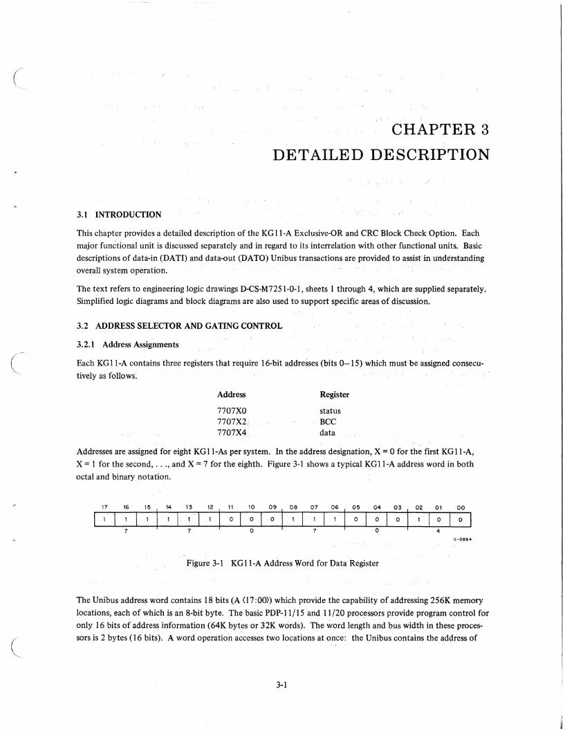
3.2.1 Address Assignments
Each KG II-A contains three registers that require 16-bit addresses (bits 0-15) which must be assigned consecu
tively as follows.
Address
7707XO 7707X2· 7707X4
Register
status Bee data
Addresses are assigned for eight KG II-As per system. In the address designation, X = 0 for the first KG II-A,
X = I for the second, ... , and X = 7 for the eighth. Figure 3-1 shows a typical KG II-A address word in both
octal and binary notation.
17 16 15 14 13 12 11 10 09 08 07 06 05 04 03 02 01 00
1 I 1 I 1 I 0
7 7 o 7 o 4 11-0884
Figure 3-1 KG II-A Address Word for Data Register
The Unibus address word contains 18 bits (A (17: 00» which provide the capability of addressing 256K memory
locations, each of which is an 8-bit byte. The basic PDP-II / I 5 and 11/20 processors provide program control for
only 16 bits of address information (64K bytes or 32K words). The word length and bus width in these proces
sors is 2 bytes (16 bits). A word operation accesses two locations at once: the Unibus contains the address of
3-1

the even·numbered location only andthe next higher odd location is selected, as well, to provide a 16·bit word.
A byte operation (DATOB) accesses any location (odd or even numbered) to select a byte (8 bits).
Assuming the use of a PDP· 1 1/ 15 or PDP" 11/20 processor with a maxiinumof64K memory locations, bits
A (17 :16> are forced to Is if bits A (IS :.13) are all I s when the processor is master. With bits A (17: 13) allis, the
last 8K·byte locations are relocated to become the highest locations accessible by the bus. All device addresses and
internal processor locations are assigned in these 8K locations. The assigned addresses for the KG II·A registers
are in these locations.
3.2.2 AddreSs Selector and Gating Control
The address selection logic is shown in drawing M7251 ,sheet 4. It is functionally equivalent to the standard
PDp· 1 I M105 Address Selector Module; its input/output pin designations are identical to the MI05.
The M7251 address selection logic uses only three of the four select signals (SELO; SEL2, and SEL4); SEL6 is not
used. It uses only two of the three gating signals (IN and OUT LOW); OUT HIGH is not used. The KG II·A
operates as a slave device only. It uses only two bus transactions: data·in(DATI) which transfers (reads) a 16~bit
data word from the KG II·A (slave) to some master device; and data-out (DATO) which transfers(writes) a 16-bit
data word from some master device to the KGIl·A (slave).
Control lines COl and COO and address line AOO determine the type of bus· data transfer to be implemented .. In
the case of the KG II-A, only DATI and DATOare used, so the state of AOO is irrelevant. Bit AOO is the byte
control bit and it has an effect only when COl and COO both equal 1. The state of AOO when COl = COO = I determines which byte (low or high) is accessed during a data-out byte (DATOB) transaction. TheDATQB trans
action is not used in operating the KGII-A. Control bits COl and COO and address bit AOO are inputs to the
address selection logic (drawing M7251 ,sheet 4). They.generate three gating signals: IN H, OUT LOW H, and
OUT HIGH H. Table 3-1 shows the gating signals generated by the two bus transactions (DATO and DATI) used
by the KG 11 -A.
Mode Control C (01:00)
00 01
Table 3-1
KGII-A Gating SignalS
Byte Control Bus Data
AOO Transfer
X DATI X PATO
Gating Signal
True (+3V)
INH OUT LOW H OUTHIGHH· (not used)
The first five digits of the address indicate which KG 1 I-A in the system has been addressed, Using the example in
Figure 3-1, the frrst five digits, 77070, indicate that the Jirst KG11·A in the system has been addressed. Octal
77070 represents bits A (17:03) which are inputs to the address selecti~n logic (drawing M7251 ,sheet 4). to
conform to the established address boupds for device registers, bits A (17: 13) must all be I s. Decoding of bits
A (I 2 :03) is determined by jumpers. If a line contains a jump¢r, the decoding logic searches for a 0 on that line;
if there is no jumper, it searches for a 1. In this example, jumpers would be installed in bit positions 11, 10, 9, 5,
4 and 3. When the processor asserts the address that matches the jumper configuration,the decoder associated
with bits A (12:03) produces a high, This signal is used in the bus control and SELECT signal portions of the
address selection logic. The decoder is a unique circuit and is discussed below,
3-2
(
(
(
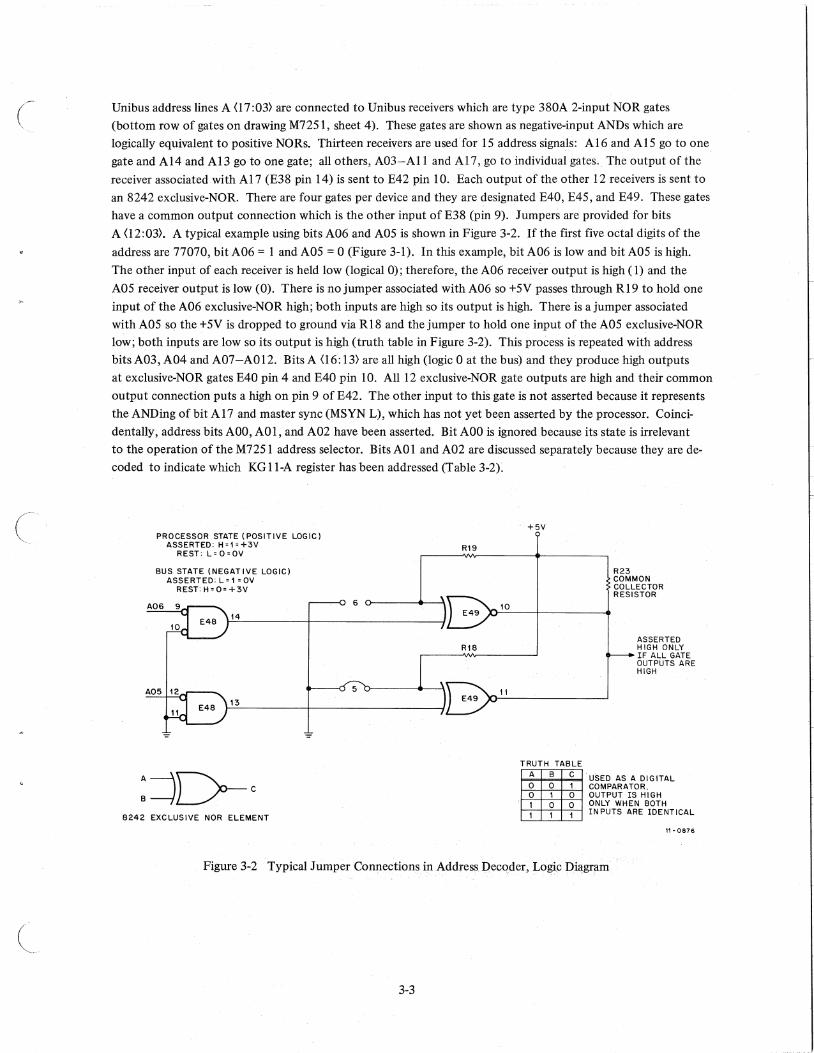
(~ Unibus address lines A (17 :03) are connected to Unibus receivers which are type 380A 2-input NOR gates
(bottom row of gates on drawing M72Sl, sheet4). These gates are shown as negative-input ANDs which are
logically equivalent to positive NORs. Thirteen receivers are used for 15 address signals: A16 and AlS go to one
gate and A14 and A13 go to one gate; all others, A03-All and A17, go to individual gates. The output of the
receiver associated with A17 (E38 pin 14) is sent to E42 pin 10. Each output of the other 12 receivers is sent to
an 8242 exclusive-NOR. There are four gates per device and they are designated E40, E4S, and E49. These gates
have a common output connection which is the other input of E38 (pin 9). Jumpers are provided for bits
A (12:03). A typical example using bits A06 and AOS is shown in Figure 3-2. If the fIrst five octal digits of the
address are 77070, bit A06 = 1 and AOS = 0 (Figure 3-1). In this example, bit A06 is low and bit AOS is high.
The other input of each receiver is held low (logical 0); therefore, the A06 receiver output is high (1) and the
AOS receiver output is low (0). There is no jumper associated with A06 so +SV passes through R 19 to hold one
input of the A06 exclusive-NOR high; both inputs are high so its output is high. There is a jumper associated
with AOS so the +SV is dropped to ground via R18 and the jumper to hold one input of the AOS exclusive-NOR low; both inputs are low so its output is high (truth table in Figure 3-2). This process is repeated with address
bits A03, A04 and A07-A012. Bits A (16: 13) are all high (logic 0 at the bus) and they produce high outputs
at exclusive-NOR gates E40 pin 4 and E40 pin 10. All 12 exclusive-NOR gate outputs are high and theIr common
output connection puts a high on pin 9 of E42. The other input to this gate is not asserted because it represents
the ANDing of bit A17 and master sync (MSYN L), which has not yet been asserted by the processor. Coinci
dentally, address bits AOO, AOl, and A02 have been asserted. Bit AOO is ignored because its state is irrelevant
to the operation of the M72Sl address selector. Bits AO 1 and A02 are discussed separately because they are decoded to indicate which KG ll-A register has been addressed (Table 3-2).
PROCESSOR STATE (POSITIVE LOGIC) ASSERTED: H=1=+3V
REST: L=O=OV
BUS STATE (NEGATIVE LOGIC) ASSERTED:L=1=OV
REST: H = 0= +3V
14
6
A05 ...._--0 5
13
:=JD-C 8242 EXCLUSIVE NOR ELEMENT
R19
10
R18
11
.. +5V
TRUTH TABLE A B C 0 0 1 0 1 0 1 0 0 1 1 1
R23 COMMON COLLECTOR RESISTOR
ASSERTED HIGH ONLY IF ALL GATE OUTPUTS ARE HIGH
USED AS A DIGITAL COMPARATOR. OUTPUT IS HIGH ONLY WHEN BOTH INPUTS ARE IDENTICAL
11-0876
Figure 3-2 Typical Jumper Connections in Address PecQder, Logic Di~grilm
3-3

Device
Address
770700 770702 770704
Table 3-2
KGl1-A Select Signals
Lines Select Signal
A <02:01> True (+3V)
00 SELECT 0 01 SELECT 2 10 SELECT 4
Register
Selected
status BCC data
Bits A02 and AOI are sent to separate Unibus receivers designated E37. The outputs of these receivers and their
complements (via two gates E42) are sent to four 4-input type 8815 NOR gates E46 (2) and E47 (2). The gates
are arranged so that only one has three low inputs for a particular combination of bits A02 and AOI (four com
binations possible). The fourth input must be low to assert the gate; this fourth input is common to all four gates
and is the output (pin 8) of E42. If the bus is clear, SSYN L is clear and the processor asserts MSYN L to the
address selection logic which produces a high at the output (pin 14) of receiver E38. This high is ANDed with the
high signal from the common connection of the exclusive-NOR gates to enable E42 pin B low. This signal enables
one of four SELECT signals, depending on the states of A02 and AOl. This low signal is also inverted by E41
pin I and asserts SSYN L from pin 4 of E41.
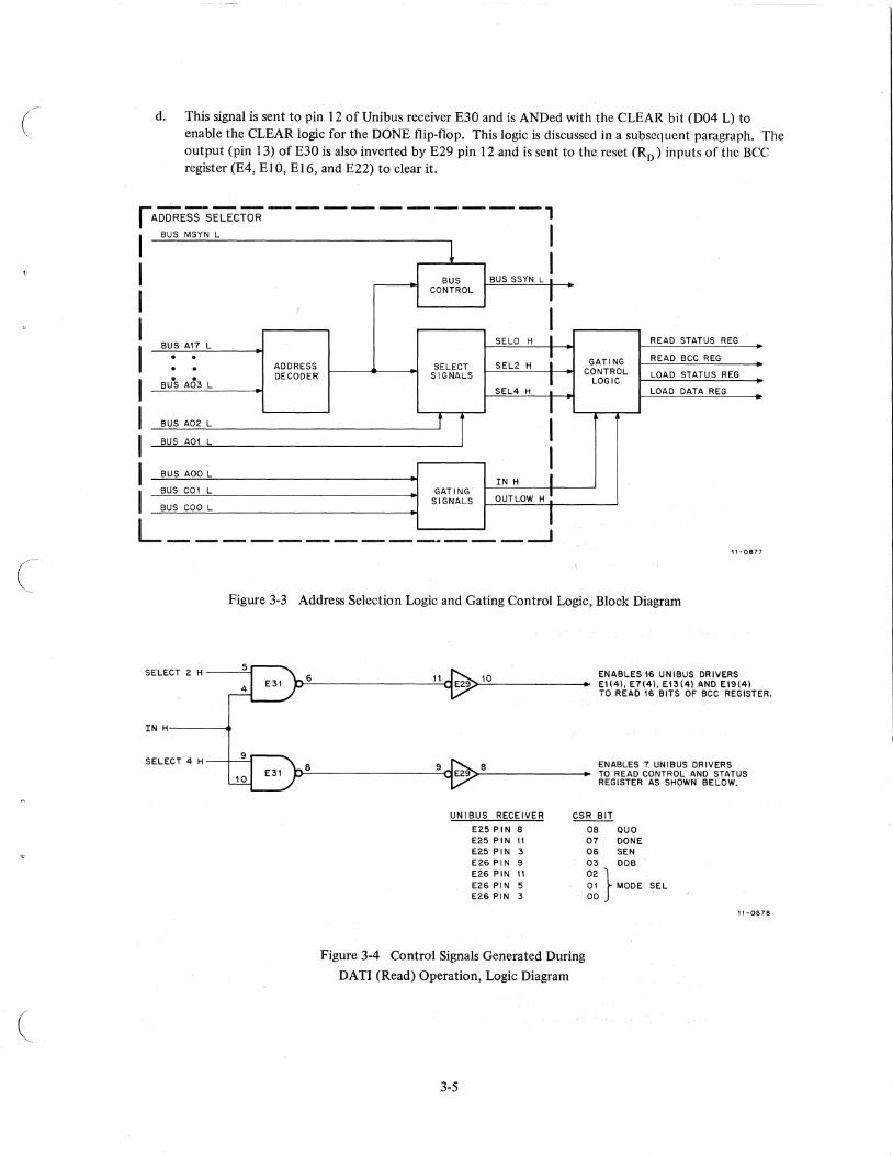
3.2.3 Gating Control Logic
The select signals and gating signals from the address selection logic are combined in a control logic network to
provide signals to implement the following functions: read/write CSR; read the BCC register; and load the data
register. Figure 3-3 is a simplified block diagram showing the interrelation of the address selection logic and the
gating control logic. The gating control logic is simple but it is spread over sheets 2 and 3 of engineering drawing
M7251. Supplemental simplified logic diagrams are used to assist in understanding the operation of the gating
control logic.
Figure 3-4 shows the control signals generated during a DATI (read) operation (drawing M7251, sheet 3). A
DATI bus transaction asserts IN H which is ANDed with SELECT 0 H or SELECT 2 H, depending on whether the
CSR or the BCC register has been addressed. If SELECT 0 is asserted, a high signal is produced at E29 pin 8 to
enable the Unibus drivers associated with the seven bits of the CSR that can be read. Enabling the drivers places
the information on the bus data lines DOO-D03 and D06-DOB. If SELECT 2 is asserted, a high signal is produced
at E29 pin 10 to enable the Unibus drivers associated with the 16-bit BCC register.
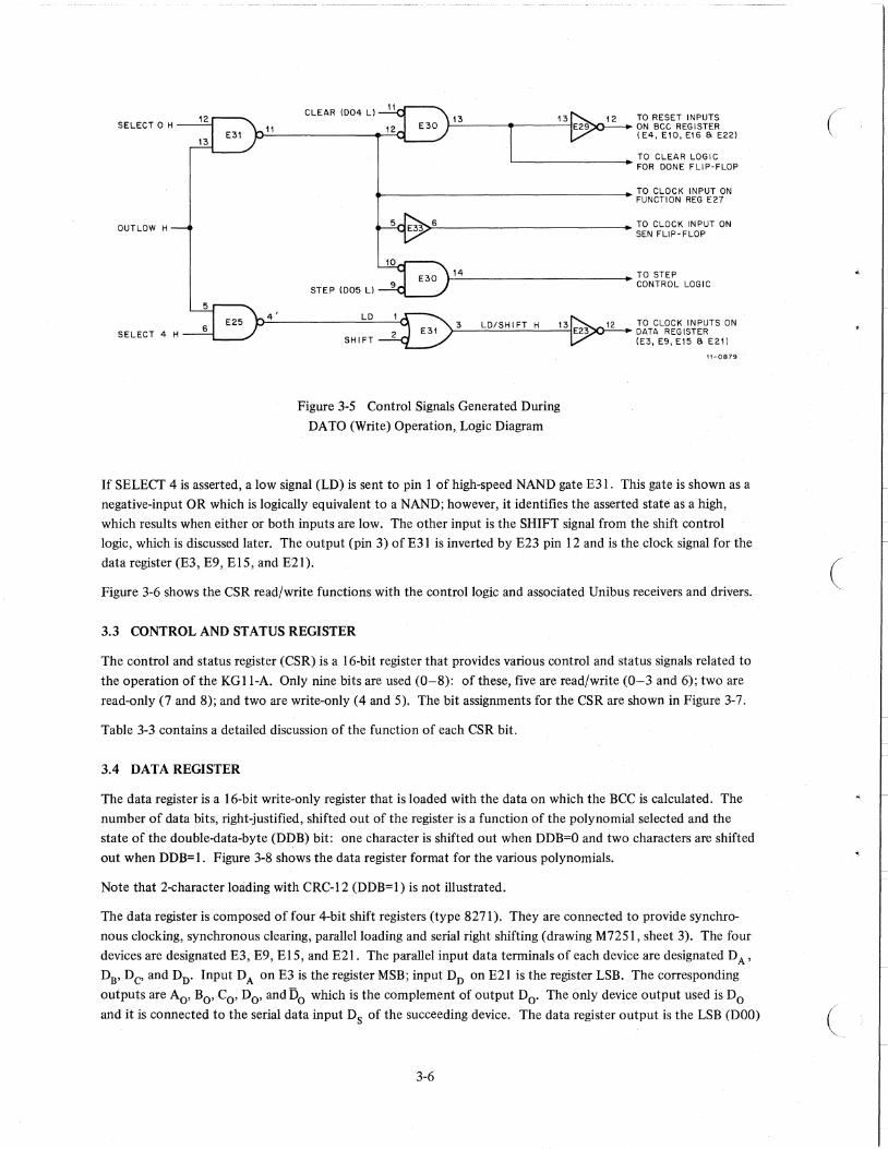
Figure 3-5 shows the control signals generated during a DATO (write) operation (drawing M7251, sheet 2).
A DATO bus transaction asserts OUT LOW H which is ANDed with SELECT 0 H or SELECT 4 H, depending on
whether the CSR or the data register has been addressed. If SELECT 0 H is asserted, a low signal is produced at
the output (pin 11) of NAND gate E31. This signal initiates several control signals.
a. It is sent directly to the CLOCK input (pin 6) of function register E27 which allows bits DOO-D03 to be written in the CSR.
b. Inversion of this signal by E33 pin 6 provides the clocking signal for the SEN flip-flop E36 pin 3 (SEN is bit D06 of the CSR).
c. This signal is sent to pin 10 of Unibus receiver E30 and is ANDed with the STEP bit (DOS L) to enable the STEP control logic. This logic is discussed in a subsequent paragraph.
(continued on next page)
3-4
(
c
(
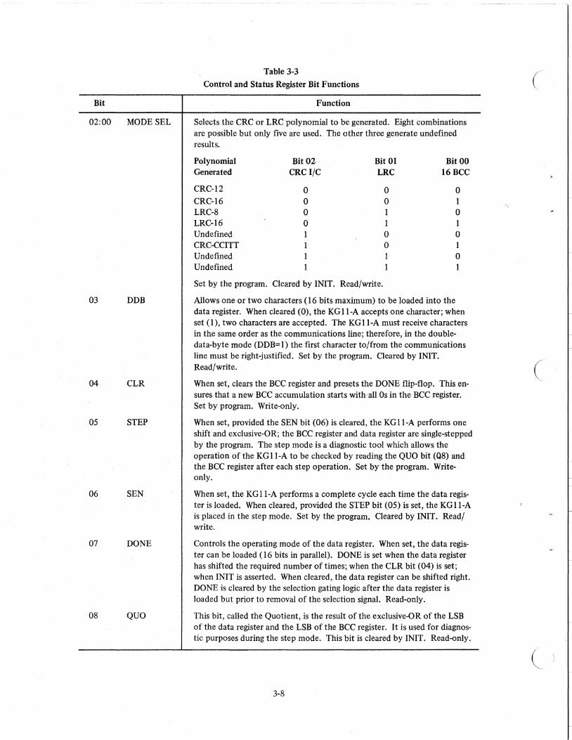
d. This signal is sent to pin 12 of Unibus receiver E30 and is ANDed with the CLEAR bit (D04 L) to enable the CLEAR logic for the DONE flip-flop. This logic is discussed in a subsequent paragraph. The output (pin 13) of E30 is also inverted by E29 pin 12 and is sent to the reset (Ro) inputs of the BCC register (E4, ElO, E16, and E22) to clear it.
rADDRESSSrucTOR - - - - - - - - ----, I BUS MSYN L I
I I I I I I I I I
BUS A17 L
· · · · · · BUS A03 L
BUS A02 L
BUS AOI L
BUS AOO L
BUS COl L
BUS COO L
1 BUS
CONTROL
(
ADDRESS SELECT DECODER SIGNALS
t I GATING
SIGNALS
I BUS SSYN L I
I I
SELO H I READ STATUS REG
: GATI NG READ BCC REG SEL2 H
CONTROL
! LOAD STATUS REG
LOGIC SEL4 H LOAD DATA REG
I I I
IN H I OUTLOW H!
I L _____________ ---.J
Figure 3-3 Address Selection Logic and Gating Control Logic, Block Diagram
SELECT 2 H ----"-I
IN H---......
SELECT 4 H ---+-....::...t
~6~--------------~I'~E29~1~0~-----. ENABLES 16 UNIBUS DRIVERS E1(4). E1(4). EI3(4) AND Et9(4) TO READ 16 BITS OF BCC REGISTER.
~8~--------------~9~E29~8~------. ENABLES 1 UNIBUS DRIVERS TO READ CONTROL AND STATUS REGISTER AS SHOWN BELOW.
UNIBUS RECEIVER
E25 PIN 8
CSR BIT
E25 PIN 11 E25 PIN 3 E26 PIN 9 E26 PIN 11 E26 PIN 5 E26 PIN 3
Figure 3-4 Control Signals Generated During
DATI (Read) Operation, Logic Diagram
3-5
08 QUO 01 DONE 06 SEN 03 DDB'
~~ } MODE SEL 00
it -0878
SELECT 0 H 11
OUTLOW H
4'
SELECT 4 H
CLEAR (D04 L)
14
STEP (D05 L)
LD 3 LD/SH I FT H
SHIFT
Figure 3-5 Control Signals Generated During
DA TO (Write) Operation, Logic Diagram
12 TO RESET INPUTS ON Bce REGISTER (E4, E10, E16 S E22)
TO CLEAR LOGIC FOR DONE FLIP-FLOP
TO CLOCK INPUT ON FUNCTION REG E27
TO CLOCK INPUT ON SEN FLIP-FLOP
TO STEP CONTROL LOG I C
TO CLOCK INPUTS ON DATA REG ISTER (E3, E9, E15 S E21l
11-0879
If SELECT 4 is asserted, a low signal (LD) is sent to pin 1 of high-speed NAND gate E31. This gate is shown as a
negative-input OR which is logically equivalent to a NAND; however, it identifies the asserted state as a high,
which results when either or both inputs are low. The other input is the SHIFT signal from the shift control
logic, which is discussed later. The output (pin 3) of E31 is inverted by E23 pin 12 and is the clock signal for the
data register (E3, E9, E15, and E21).
Figure 3-6 shows the CSR read/write functions with the control logic and associated Unibus receivers and drivers.
3.3 CONTROL AND STATUS REGISTER
The control and status register (CSR) is a 16-bit register that provides various control and status signals related to
the operation of the KG II-A. Only nine bits are used (0-8): of these, five are read/write (0-3 and 6); two are
read-only (7 and 8); and two are write-only (4 and 5). The bit assignments for the CSR are shown in Figure 3-7.
Table 3-3 contains a detailed discussion of the function of each CSR bit.
3.4 DATA REGISTER
The data register is a 16-bit write-only register that is loaded with the data on which the BCC is calculated. The
number of data bits, right-justified, shifted out of the register is a function of the polynomial selected and the
state of the double-data-byte (DDB) bit: one character is shifted out when DDB=O and two characters are shifted
out when DDB=l. Figure 3-8 shows the data register format for the various polynomials.
Note that 2-character loading with CRC-12 (DDB=I) is not illustrated.
The data register is composed of four 4-bit shift registers (type 8271). They are connected to provide synchro
nous clocking, synchronous clearing, parallel loading and serial right shifting (drawing M7251 , sheet 3). The four
devices are designated E3, E9, E15, and E21. The parallel input data terminals of each device are designated D A'
DB' Dc' and DD' Input DA on E3 is the register MSB; input DD on E21 is the register LSB. The corresponding
outputs are Ao' Bo' Co' Do' and Do which is the complement of output Do' The only device output used is Do and it is connected to the serial data input Ds of the succeeding device. The data register output is the LSB (DOO)
3-6
(
.,
(
(

(
(
SELECT 0 H
OUT LOW H
SELECT 0 H
IN H
15 14
( '---
DATO (WRITE)
000
002
004
13
3
13
14
6
15
2
3
3
UNIS:US
DO DO
DC Co 9
E27 FUNCTION
GENERATION
DB BO 7
DA AO 5
CLK
6
I 5
E36 SEN FLIP FLOP
CLK o 6
} 000""" TO INTERNAL LOGIC
8CC LSB ED
DATA LS8
DATI (READ)
000
DOl
002
006
4
13
10
TO INTERNAL LOGIC
007
13
008
10
E14, E20 AND E30 ARE UNIBUS RECEIVERS
E25 AND E26 ARE UNIBUS DRIVERS
Figure 3-6 Control and Status Read/Write Functions, Logic Diagram
13 12 11 02 01 00
NOT USED MODE SEL
R/W R/W R/W
1i-0880
11-0881
Figure 3-7 Control and Status Register Bit Assignments
3-7
Bit
02:00 MODESEL
03 DDB
04 CLR
05 STEP
06 SEN
07 DONE
08 QUO
Table 3-3
Control and Status Register Bit Functions
Function
Selects the CRC or LRC polynomial to be generated. Eight combinations are possible but only five are used. The other three generate undefined results.
Polynomial Generated
CRC-12
CRC-16 LRC-8 LRC-16 Undefined CRC-CCITT Undefined Undefined
Bit 02 CRCI/C
o o o o
Bit 01 LRC
o o
1 o o
Set by the program. Cleared by INIT. Read/write.
Bit 00 16BCC
o 1 o 1 o I o
Allows one or two characters (16 bits maximum) to be loaded into the data register. When cleared (0), the KG Il-A accepts one character; when set (1), two characters are accepted. The KG 1 I-A must receive characters in the same order as the communications line; therefore, in the doubledata-byte mode (DDB=l) the first character to/from the communications line must be right-justified. Set by the program. Cleared by INIT. Read/write.
When set, clears the BCC register and presets the DONE flip-flop. This ensures that a new BCC accumulation starts with all Os in the BCC register. Set by program. Write-only.
When set, provided the SEN bit (06) is cleared, the KG ll-A performs one shift and exclusive-OR; the BCC register and data register are single-stepped by the program. The step mode is a diagnostic tool which allows the operation of the KG ll-A to be checked by reading the QUO bit (Q8) and the BCC register after each step operation. Set by the program. Writeonly.
When set, the KG ll-A performs a complete cycle each time the data register is loaded. When cleared, provided the STEP bit (05) is set, the KG ll-A is placed in the step mode. Set by the program. Cleared by INIT. Read/ write.
Controls the operating mode of the data register. When set, the data register can be loaded (16 bits in parallel). DONE is set when the data register has shifted the required number of times; when the CLR bit .(04) is set; when INIT is asserted. When cleared, the data register can be shifted right. DONE is cleared by the selection gating logic after the data register is loaded but prior to removal of the selection signal. Read-only.
This bit, called the Quotient, is the result of the exclusive-DR of the LSB of the data register and the LSB of the BCC register. It is used for diagnostic purposes during the step mode. This bit is cleared by INIT. Read-only.
3-8
c
II

(~
(
c
13 12 11 10 09 08 07 06 05 04 I 03 I 02 I 01
•
CRC-12 (DDB=O)
LRC-8,LCR-1S;CRC-16 AND CRC-CCITT(DDB=O)
LRC-8,LRCI6 ,CRC -16 AND CR(:-CCITT( DDB= 1)
Figure 3-8 Data Register Format
LSB
00
11-0882
from output Do of E21. The register is cleared by INIT L applied to the direct reset (RD) input of each device.
The register is clocked on the negative-going transition of the clock pulse which is the inverted LD/SHIFT H
signal from pin 12 of high-speed inverter E23. The clock pulses originate in the logic shown in drawing M7251 ,
sheet 2. This logic is discussed in detail in subsequent paragraphs. Briefly, a clock pulse is generated when the
data register is addressed (SELECT 4 H and OUT LOW H are asserted). This pulse loads the register with the 16
data bits on the data lines (D (I 5: 00» via Unibus drivers. After the register is loaded, clock pulses are generated
to shift the data register a specific number of times. The mode of operation of the data register is controlled by
the load (LD) and shift (SFT) inputs. Type 8271 shift registers can be operated in four modes, depending on the
status of LD and SFT. In this appiication, only two modes of operation are used and the controlling factor is the
shift (SFT) input. The load (LD) input of each device is connected to +3V which holds it high (1). The shift
(SFT) inputs are all tied to DONE (1) L which is the 0 output of the DONE flip-flop. When the DONE flip-flop
is set, DONE (l) L = 0 and the parallel load mode is selected; the serial shift right mode is selected when the
DONE flip-flop is cleared and DONE (1) L = 1.
3.5 BLOCK CHECK CHARACTER (BCC) REGISTER
The block check character (BCC) register is a 16-bit read-only register which maintains the accumulation (block
check character) derived from the shifting operations. The format of the data in the BCC register is a function of
the polynomial used to perform the accumulation. Figure 3-9 shows the BCC register format for the various
polynomials.
15 14 13 I 12 I 11 I 10 I 09 I 08 07 06 05 I 04 I 03 I 02 I 01 I 00
LS8 MSB
CRC-16 (2ND CHAR) CRC-CCITT (2ND CHAR)
• LRC-16
CRC-12 (;sr CHAR)
CRC-16(isr CHAR) CRC-CCITT(ISr CHAR)
LRC-8
Figure 3-9 BCC Register Format
11-0883
The BCC register is composed of four 4-bit shift registers (type 8271) designated E4, El 0, E16, and E22. They are
connected to provide synchronous clocking and synchronous clearing (drawing M7251, sheet 3). The register is
cleared by CLEAR BCC L which is generated when the CLEAR bit (D04) is set or INIT is asserted. The
CLEAR BCC L signal is sent to the direct reset (RD) input of each device. The register is clocked on the
3-9

negative-going transition of the clock pulse which is the output (pin 6) of inverter E 17 (drawing M72S1 , sheet 2).
This clock pulse originates in logic that is discussed in det~ in subsequent paragraphs. The BCC register is
operated in two modes only and the controlling factor is the shift (SFT) input; the load (LD) input of each device
is connected to +3V which holds it high (1). The shift inputs of E10 (bits D11 through 008) and E22 (bits 003
through 000) are connected to LRC (1) H which is mode-select bit 001 from E27. When LRC (1) H = 1, the
serial shift right mode is selected; the parallel load mode is selected when LRC (1) H = O. The shift input of E 16
(bits 007 through 004) is connected to 16 BCC (1) H. When 16 BCC (1) H = 1, the serial shift right mode is
selected; the IJarallelioad mode is selected when 16 BCC (1) H = O. Signal LRC (1) H is inverted and applied to
pin 2 of NAND gate E 18 along with CRC I/C L which is mode-select bit 002 from E27. The output (pin 3) of
E18 is sent to the shift input ofE4 (bits 015 through D12). When either or both inputs ofEI8 are low, its output is high and E4 is placed in the serial shift right mode. Both inputs must be high to select the parallel load mode.
A different feedback connection is used to accumulate the BCC for each polynomial. Sample accumulations and hardware configurations are discussed in detail in Appendix A.
3.6 CONTROL SIGNALS GENERATED BY THE CSR
3.6.1 Introduction
The first seven bits (006-000) of the CSR can be written into to perform certain functions (Table 3-3). The
following paragraphs discuss the logic that generates the signals required to perform the functions.
3.6.2 Mode Selection Bits 002:00 and DDB Bit 003
Bits 0 <03: 00> are sent to the inputs of E27 which is a 4-bit shift register (type 8271). The shift (SFT) input is
connected to ground (logical 0) and the load (LD) input is connected to +3V (logical 1). As a result of these
connections, E27 operates only in the parallel load mode (drawing M72SI, sheet 2). The input data is transferred
to the output on the negative-going clock transition. The device is clocked when the CSR is addressed during a
DATO operation (SEL 0 H and OUT LOW H are both high). Bit-to-signal correspondence is:
Bit Signal
000 16 BCC (1) 001 LRC 002 CRC I/C 003 DDB
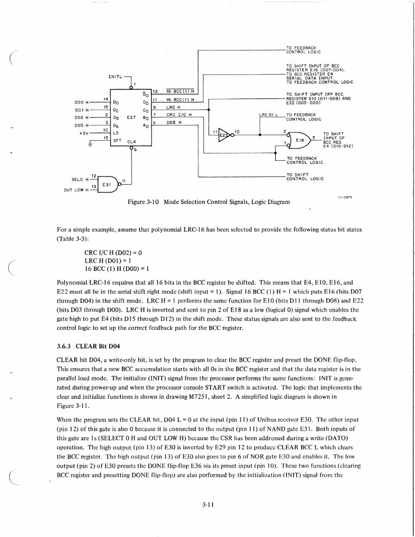
A simplified logic diagram of E27 and associated gates is shown in Figure 3-10. DDB H (E27 pin 5) goes to the
shift control logic where it and its complement (DDB L) are used (E34 pins 3 and 4). Signal 16 BCC (I) H goes
to the shift input of BCC register El6 (bits 007 through 004) and pin 12 of NAND gate E18, which is in the line
to the serial data input (Os) of BCC register E4 (bits DIS through 012). Along with its complement, output Do (pin 12) of E27, 16 BCC (1) H also goes to the feedback selection logic. LRC H goes to the shift inputs of BCC
register El 0 (bits D11 through 008) and E22 (bits 003 through 000). It is inverted by E23 pin 10 and is sent as
LRC (1) L to the feedback selection logic. LRC (I) L is also applied to NAND gate EI8 pin 2. The other input
(pin 1) of El8 is CRC I/C H. When either or both inputs are low, E 18 is enabled high to the shift input of BCC
register E4 (bits 015 through D 12). CRC l/C H is also sent to the feedback selection logic.
(
(
><,1\
(
('-
TO FEEDBACK CONTROL LOGIC
TO SHIFT INPUT OF BCC REGISTER EI6 (007-004). TO BCC REGISTER E4
INITL SERIAL DATA INPUT. TO FEEDBACK CONTROL LOGIC
DO 12 16 BCC (1) H
TO SH I FT INPUT OFF BCC 14 11 . 16 BCC( 1) H REGI STER ElO (011- 008) AND
000 H DO DO E22 (003-000)
001 H 15
DC Co 9 LRC H
002 H 2
DB E27 BO 7 CRC I1C H TO FEEDBACK
CONTROL LOGIC
003 H 3
DA AO 5 DDB H
10 LD +3V TO SHIFT
13 SFT
INPUT OF CLK BCC REG.
E4 (015-012) 6
SELO H
OUT LOW H
11-0675
Figure 3-10 Mode Selection Control Signals, Logic Diagram
For a simple example, assume that polynomial LRC-16 has been selected to provide the following status bit states
(Table 3-3):
CRC IjC H (D02) = 0 LRC H (DOl) = 1 16 BCC (1) H (DOO) = 1
Polynomial LRC-16 requires that all 16 bits in the BCC register be shifted. This means that E4, EIO, E16, and
E22 must all be in the serial shift right mode (shift input = I). Signal 16 BCC (I) H = 1 which puts E 16 (bits 007
through D04) in the shift mode. LRC H = I performs the same function for E 10 (bits D 11 through D08) and E22
(bits D03 through DOO). LRC H is inverted and sent to pin 2 of EI8 as a low (logical 0) signal which enables the
gate high to put E4 (bits D 15 through D 12) in the shift mode. These status signals are also sent to the feedback
eontrollogie to set up the correct feedback path for the BCC register.
3.6.3 CLEAR Bit 004
CLEAR bit D04, a write-only bit, is set by the program to clear the BCC register and preset the DONE flip-flop.
This ensures that a new BCC accumulation starts with all Os in the BCC register and that the data register is in the
parallel load mode. The initialize (lNIT) signal from the processor performs the same functions: INIT is gene
rated during power-up and when the processor console START switch is activated. The logic that implements the
clear and initialize functions is shown in drawing M7251, sheet 2. A simplified logic diagram is shown in
Figure 3-11 .
When the program sets the CLEAR bit, D04 L = 0 at the input (pin 11) of Unibus receiver E30. The other input
(pin 12) of this gate is also 0 because it is connected to the output (pin 11) of NAND gate E31. Both inputs of
this gate are I s (SELECT 0 H and OUT LOW H) because the CSR has been addressed during a write fDA TO)
operation. The high output (pin 13) of E30 is inverted by E29 pin 12 to produce CLEAR BCC L which clears
the BCC register. The high output (pin 13) of E30 also goes to pin 6 of NOR gate E30 and enables it. The low
output (pin 2) of E30 presets the DONE flip-flop E36 via its preset input (pin 10). These two functions (clearing
BCC register and presetting DONE flip-flop) are also performed by the initialization (INIT) signal from the
3-11

processor. When asserted, INIT = 0 at pin 5 of Unibus receiver E30. It produces a high at output pin 3 of E30
which enables E30 pin 2 low and presets the DONE flip-flop. This high signal is inverted by E29 pin 2 to produce
CLEAR BCC L which clears the BCC register. The outputs of both inverters (E29 pin 12 and E29 pin 2) are
connected together; this common point is CLEAR BCC L. These inverters are 7416 open-collector type and are
connected in a wired-OR configuration. The output is 0 when one or both inputs equal 1. CLEAR BCC L = 0
when either CLEAR or INIT is asserted. The high output (pin 3) of E30, when INIT is asserted, is inverted by E29
pin 4 to generate INIT L = O. This signal clears the data register, SEN flip-flop E36, and E27.
(CLEAR) ____ -------.. D04L
10
PRE D
E36 DONE
CLK 0
Figure 3-11 Clear and Initialize Control Signals, Logic Diagram
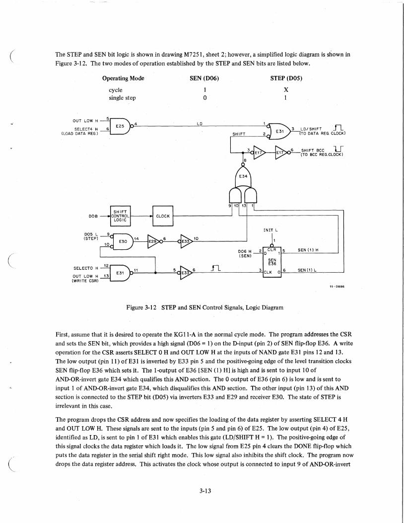
3.6.4 STEP Bit DOS and Shift Enable (SEN) Bit D06
The STEP bit and SEN bit are used to place the KG ll-A in the single-step mode, which is a diagnostic tool. Nor
mally, the KG ll-A performs a complete cycle each time the data register is loaded. If the SEN bit (D06) is
cleared, the KG ll-A performs one shift and exclusive-OR operation each time the STEP bit (DOS) is set. This
single-step mode allows the performance of the KG ll-A to be checked by examination of the contents of the
BCC register and the state of the quotient (QUO) bit DOB after each step.
The STEP and SEN bit logic interacts with the shift clock and shift control logic. In the single-step mode, the
shift clock output is inhibited. This discussion covers primarily the single-step mode; details of the shift clock
and shift control logic are discussed in. detail in Paragraph 3.6.5.
3-12
(
(
(~
The STEP and SEN bit logic is shown in drawing M72Sl, sheet 2; however, a simplified logic diagram is shown in
Figure 3-12. The two modes of operation established by the STEP and SEN bits are listed below.
OUT LOW H
SELECT4 H (LOAD DATA REG.l
DDB
005 L (STEP)
SELECTO H
OUT LOW H (WRITE CSR)
Operating Mode
cycle single step
4
SHIFT
SEN (D06)
o
LD
CONTROLf------./ CLOCK 1-----------' LOGIC
006 H (SEN)
STEP (DOS)
X
INIT L
3 LD/SHIFTJL TO DATA REG. CLOCK)
SHIFT BCC U (TO BCC REG.CLOCK)
SEN (1) H
,~~_~ ______ 3~CLK Or6~~S~E~N~('~)~L_~_~
1t-0886
Figure 3-12 STEP and SEN Control Signals, Logic Diagram
First, assume that it is desired to operate the KG ll-A in the normal cycle mode. The program addresses the CSR
and sets the SEN bit, which provides a high signal (D06 = 1) on the D-input (pin 2) of SEN flip-flop E36. A write
operation for the CSR asserts SELECT 0 H and our LOW H at the inputs of NAND gate E31 pins 12 and 13. The low output (pin 11) of E31 is inverted by E33 pin 5 and the positive-going edge of the level transition clocks
SEN flip-flop E36 which sets it. The l-output ofE36 [SEN (1) H) is high and is sent to input 10 of
AND-OR-invert gate E34 which qualifies this AND section. The 0 output of E36 (pin 6) is low and is sent to
input 1 of AND-OR-invert gate E34, which disqualifies this AND section. The other input (pin 13) of this AND
section is connected to the STEP bit (DOS) via inverters E33 and E29 and receiver E30. The state of STEP is
irrelevant in this case.
The program drops the CSR address and now specifies the loading of the data register by asserting SELECT 4 H
and our LOW H. These signals are sent to the inputs (pin S and pin 6) of E2S. The low output (pin 4) of E2S,
identified as LD, is sent to pin 1 of E3l which enables this gate (LD/SHIFT H = 1). The positive-going edge of
this signal clocks the data register which loads it. The low signal from E2S pin 4 clears the DONE flip-flop which
puts the data register in the serial shift right mode. This low signal also inhibits the shift clock. The program now
drops the data register address. This activates the clock whose output is connected to input 9 of AND-OR-invert
3-13

gate E34. The repetitive clock pulses are propagated through E34 pin 8 to pin 2 of E31. The output of this gate
is LD/SHIFT H and its positive-going transitions clock the data register. The clock pulses from E34 pin 8 are
double-inverted by El7 pin 4 and EI7 pin 6 whose output is SHIFT BCC. The negative-going transitions of
SHIFT BCC clock the BCC register. This process continues until the shifting ceases. The cycle is completed and
. the new block check character is in the BCC register.
To operate the KG II-A in the single-step mode, the program addresses the CSR and clears the SEN bit, which
places a low signal (D06 = 0) on the D-input of SEN flip-flop E36. As in the previous example (cycle mode), the
SEN flip-flop is clocked, which clears it. The I output ofE36 [SEN (1) H] is low and is sent to input 10 of
AND-OR-invert gate E34 which disqualifies this AND section and blocks the passage of shift clock pulses through
E34 pin 8. The 0 output of E36 (pin 6) is high and is sent to input I of AND-OR-invert gate E34 which qualifies
this AND section. The program drops the CSR address and now loads the data register as described in the previous
example of the cycle mode. The data register is placed in the serial shift right mode. The program now drops the
data register address; the shift clock is activated but its output is inhibited by SEN (1) H = O. To implement the
single-step mode, the program addresses the CSR and sets the STEP bit which places a low (D06L = 0) on pin 9
of Unibus receiver E30. The other input (pin 10) of the gate is connected to the output (pin II) of E31. This
output goes low when a CSR write operation is specified; SELECT 0 H and OUT LOW H are asserted (logical 1).
With both inputs (pins 9 and 10) of E30 low, its output (pin 14) is high. This signal is double-inverted by E29
pin 6 and E33 pin II, and sent to input 13 of AND-OR-invert gate E34. This AND section of E34 is enabled and
a low is produced at the output (pin 8) of E34, which enables LD/SHIFT H at pin 3 of E31 and SHIFT BCC at
pin 6 of E17. These signals clock the data register and BCC register; actually, one shift and exclusive-OR operation
has been performed. Each time the STEP bit is set by the program, a single step is performed. After each step,
the program can read the contents of the BCC register and read the quotient (QUO) bit (D08) in the CSR to check
the operation of the KG II-A. The QUO bit is the result of the exclusive-OR of the LSB of the data register and the LSB of the BCC register. This operation is performed at exclusive-OR gate E28 pin 6 (drawing M7251, sheet
3). The QUO bit can be read at Unibus driver E25 pin 10.
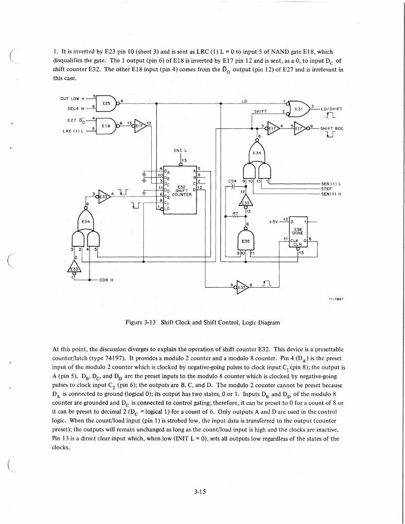
3.6.5 Shift Clock and Shift Control Logic
In performing three types of cyclic redundancy checks (CRC) and two forms of longitudinal redundancy checks
(LRC), the KG II-A deals with 6-bit, 8-bit, and 16-bit characters. It has the capability of shifting the data register
and BCC register 6, 8, or 16 times, depending on the function being processed. A shift clock and shift control
logic provide the correct number of shifts. The control logic includes the shift counter E32; DONE flip-flop E36;
gating logic E33, E34, and E35; and counter preset gates EI7 and EI8 (drawing M7251, sheet 2, lower left
section). A simplified logic diagram is provided in Figure 3-13.
The shift clock is a simple IO-MHz RC type. It consists of NAND gate E35, inverter E33, and feedback capacitor
C54 and resistor R7. The clock output, E33 pin 12, is fed back via C54 to input pin 9 of E35. The other two
inputs to this 3-input NAND gate are the 0 output [DONE (I) LJ of the DONE flip-flop and the output of E25
(pin 4), which is the ANDing of SELECT 4 H and OUT LOW H. The qualifying conditions for starting the clock are: SELECT 4 H = 0 (data register not selected), and DONE (1) L =J (DONE flip-flop cleared). The clock is
stopped after the correct number of shift pulses by the DONE flip-flop, which is set by the overflow pulse from the shift counter.
For example, assume that polynomial LRC-8 is selected and that single 8-bit characters are to be loaded
(DDB = 0). The SEN bit (D06) is set which places the KGII-A in the normal cycle mode. The program deter
mines the mode selection bits for LRC-8: DOOH = 0, DOIH = I, D02 H = 0, and D03H = 0 (single 8-bit character selection). The program selects a write CSR operation (SELECT 0 H and OUT LOW H are asserted), which clocks
E27 and transfers the input data (DOOH - D03H) to the output. Output pin 9 of E27 is LRC H (bit DOl) and is
3-14
(
(
l
(
c
1. It is inverted by E23 pin 10 (sheet 3) and is sent as LRC (1) L = 0 to input 5 of NAND gate E18, which
disqualifies the gate. The I output (pin 6) of E18 is inverted by E17 pin 12 and is sent, as a 0, to input Dc of
shift counter E32. The other E 18 input (pin 4) comes from the Do output (pin 12) of E27 and is irrelevant in
this case.
OUT LOW H
SEL4 H
E27 Dc;
LRC (1) L
4
INI L
13
r-+--f-4'-lO A A 5
r--f--+'1'=-jO 0 B 9 3 B C 2
DC
U r----+1'-"t1 DO S~~~T 0 12 >-_=-__ -=--_t---=-i6 C2 COUNTER
r---1-B,.,c, U 1 LO
LO/SHIFT
fl
SHIFT BCC
U
'---------SEN (1) L '----------STEP
L----------SEN(1) H
L-__ ----:!..9a E33,>=8 __ Jl_---'
11-0887
Figure 3-13 Shift Clock and Shift Control, Logic Diagram
At thIs point, the discussion diverges to explain .the operation of shift counter E32. This device is a presettable
counter/latch (type 74197). It provides a modulo 2 counter and a modulo 8 counter. Pin 4 (D A) is the preset
input of the modulo 2 counter which is clocked by negative-going pulses to clock input C1 (pin 8); the output is
A (pin 5). DB' Dc' and Dn are the preset inputs to the modulo 8 counter which is clocked by negative-going
pulses.to clock input C2 (pin 6);.the outputs are B, C, and D. The modulo 2 counter cannot be preset because
DAis connected to ground (logical 0); its output has two states, 0 or I. Inputs DB and Dn of the modulo 8
counter are grounded and Dc is connected to control gating; therefore, it can be preset to 0 for a count of 8 or
it can be preset to decimal 2 (Dc = logical 1) for a count of 6. Only outputs A and D are used in the control
logic. When the count/load input (pin 1) is strobed low, the input data is transferred to the output (counter
preset); the outputs will remain unchanged as long as the count/load input is high and the clocks are inactive.
Pin 13 is a direct clear input which, when low (INIT L = 0), sets all outputs low regardless of the states of the
clocks.
3-15
The discussion now returns to the point at which the modulo 8 counter input Dc is a 0 (via El7 pin 12). The ('
program drops the write CSR operation and selects the load data register operation. SELECT 4 H and OUT LOW H
are asserted (both = 1) which produces a low at the output (pin 4) of E25. This low enables LD/SHIFT H = 1
which clocks the information on the data lines D <07 :00> to the output of the data register. It also clears the
DONE flip-flop, which puts the data register in the serial shift right mode; there is enough delay in the circuit to
ensure loading of the data register prior to its change to the shift mode. The low signal from E25 pin 4 is sent to
the count/load input (pin 1) of the shift counter E32 which strobes the input data to the output; in this case, the
counter is preset to O. With the DONE flip-flop cleared, DONE (1) L = 1 and is sent to the shift clock input (E35
pin 11). Input 10 is sti1110w, so the output (pin 8) of E35 is high and is fed back to input 9 via resistor R7. When
the program drops the load data register operation, input 10 goes high and the clock starts. The oscillations are
sustained by the RC network as long as inputs 10 and 11 remain high. The clock pulses are produced at the
output (pin 12) of E33 at a rate of 10 MHz. The clock pulses are propagated through AND-OR-invert gate E34
via input 9. This AND section is qualified by a high at input 10 from the SEN flip-flop 1 output (pin 5) which is
high because the flip-flop is set (normal cycle mode of KG II-A). The 0 output (pin 6) of the SEN flip-flop is low
and is sent to input 1 of E34, which disqualifies this AND section. The clock pulses from E34 pin 8 enable
LD/SHIFT H and SHIFT BCC to shift the data register and the BCC register. The modulo 2 counter is incre-
mented by the clock pulses received at clock input C1 (pin 8 of E32).
The clock pulses are also sent to input 2 of AND-OR-invert gate E34 which is qualified by a high from E33 pin 2.
The input to this inverter is DDB = 0 which specifies that 8-bit characters are to be processed. The clock pulses
are propagated through E34 pin 6, inverted by E33 pin 4, and sent to clock input C2 (pin 6 of E32). The modulo
8 counter is incremented. Output A alternates between 0 and 1 and is sent to input 5 of the other AND section
of E34. The state of the modulo 2 counter (output A) is irrelevant because this AND section is disqualified by a
low on input 4 (DDB = 0).
The shift clock is running and each pulse causes the data register and BCC register to shift once; each pulse also
increments the modulo 8 counter by 1. The counter started at 0 and the eighth clock pulse causes it to overflow
(go to all Os). This produces a negative-going edge at the D output (E32 pin 12) Which is inverted by E33 pin 8;
the resulting positive-going edge clocks the DONE flip-flop, which sets it. The 0 output of the DONE flip-flop
[DONE (1) L], which is connected to the clock input (E35 pin 11), goes low and stops the clock. This signal also
places the data register in the parallel load mode to await the next character. After the required eight shifts, the
clock is stopped and is ready to begin the next cycle. Figure 3-14 shows the counter states and the generation of
the overflow signal that turns off the clock.
If the example had selected polynomial CRC-12 with 6-bit characters to be handled (DDB = 0), the operating
cycle would be the same except that the counter would be preset to 210 and the clock would be stopped after six
shift pulses.
To explain a 16-shift operation, assume that polynomial CRC-16 is selected and that two 8-bit characters are to
be loaded (DDB = 1). The mode selection is made for CRC-16: DOOH = 1, DO 1 H = 0, D02H = 0, and D03H = 1
(two 8-bit character selection). The data register is loaded with 16 bits, the DONE flip-flop is cleared, the modulo
8 counter is preset to 0, and the shift clock is started. The clock pulses from E34 pin 8 enable LD/SHIFT Hand
SHIFT BCC to shift the data register and the BCC register. DDB'" 1 and is sent to input 4 of AND-OR-invert gate
E34, which qualifies this AND section; the other AND section of this gate is disqualified by the inverted DDB
signal (0) applied to input 3. The clock pulses from E34 pin 8 are sent to clock input C1 (pin 8 of E32). Each
negative-going transition of the shift clock changes the state of the modulo 2 counter (output A). The output of
this counter (pin 5 of E32) is sent to input 5 of AND-OR-invert gate E34. The pulses formed by the alternating
state changes are propagated through E34 and E33 pin 4 to clock input C2 (pin 6 of E32). Each negative-going
transition increments the modulo 8 counter by 1. After eight C2 clock pulses, the counter overflows (output
3-16

c D = 0) and the shift clock is stopped. There is one negative-going transition of C2 for two negative-going tran
sitions of the shift clock; therefore, 16 shift operations have taken place during the eight counts initiated by dock
C2 • Figure 3-15 shows the counter states and the generation of the overflow signal.
C2 CLOCK COUNTER STATES
PULSES D C B
START a a a Ll a a 1
2 a 1 a 3 a 1 1
4 1 a a 5 1 a 1
6 1 1 a 7 1 1 1
8 a a a
COUNTER ~r---- OVERFLOW
STATE (Nl0)~L-~~~~-L-L-L __
,-----,------ +3.5V COUNTER
D OUTPUT 1-------' ----- OV
E33 OUTPUT ~---, ----- +3.5V (PIN B)
C2 CLOCK PULSESL-L-L-~~~-L-L-L __
12345678
11-0888
Figure 3-14 Counter States and Overflow for Eight Shift Pulses
3.6.6 Exclusive-OR Operators and Feedback Logic
The KG 11-A performs three types of cyclic redundancy checks (CRC) and two forms of longitudinal redundancy
checks (LRC). The BCC register is used to accumulate the BCCs, but each of the five checks requires a specific
configuration of exclusive-OR (X-OR) operators and feedback paths. A logic network provides the proper configu
ration for the check mode selected (drawing M7251, sheet 2). This paragraph describes the general arrangement
of the logic; it does not describe detailed data flow. Notes in the upper-right corner of sheet 2 identify each type
of check with a circled number (1 through 5). These circled numbers are placed at various points in the logic in
sheet 2, and in the BCC register in sheet 3, to define the data paths. This convention,.along with the BCC block
diagrams and tabular shift patterns presented in Appendix A, should allow the reader to trace the data flow during
a BCC accumulation.
The outputs of the X-OR and feedback logic are applied to the data inputs of the BCC register. A typical output
signal is identified as BCC 5 IN; this sIgnal goes to the bit 05 input of the BCC register. The majority of input
signals to this logic come from the BCC register data outputs; for example, BCC 14 OUT. The mode select signals
from E27 are used as inputs: BCC (1) Hand its complement from the Do output of E27; LRC H and its comple
ment from E23 pin 10 (sheet 3); and CRC I/C H and its complement from E23 pin 2 (sheet 2). Another input is
the exclusive-OR of the LSB of the data register and the LSB of the BCC register (BCC LSB Ell DATA REG) from
E28 pin 6 (sheet 3).
3-17

COUNTER STATE (N 10)
COUNTER o OUTPUT
C2 CLOCK PULSES
C1CLOCK PULSES
Ci CLOCK C2 CLOCK PULSES PULSES
START START
Ll 2 Ll 3
4 2
5
6 3
7
8 4
9
10 5
H
12 6
13
14 7
15
16 8
0
COUNTER STATES
0 C B
0 0 0
0 0 0
0 0 i
0 0 1
0 i 0
0 i 0
0 i i
0 i i
i 0 0
1 0 0
1 0 1
1 0 1
1 i 0
i 1 0
1 1 i
1 1 1
0 0 0 COUNTER OVERFLOW
rOVERFLOW
0
1 2 3 4 5 6 7 8 9 iO 11 12 13 14 15 16
11-0889
Figure 3-15 Counter States and Overflow for 16 Shift Pulses
Most of the IC devices used in the X-OR and feedback logic are self-explanatory (NAND gates, inverters, exc1usive
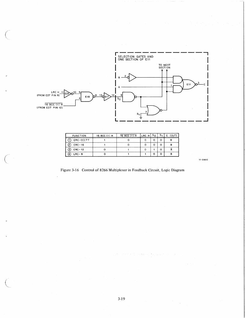
OR gates, and AND-OR-invert gates); however, one MSI device (Ell) requires a brief description. Ell is an
8266 2-Input 4-Bit Multiplexer (sheet 2, top center section). The multiplexer chooses from two different4-bit
inputs (pins 14, II, 5, and 2, or pins 15, 10, 6, and 1); selection is controlled by inputs 7 and 9. A simplified
logic diagram of one section of the multiplexer, along with the control signals, is shown in Figure 3-16. Ell con
tains four identical sections and two selection gates. Each section is an AND-OR-invert gate with an inverter in
one input leg (Figure 3-16). Input A (pin 1) goes directly to one input of a 2-input AND gate; input B (pin 2) is
inverted and then goes to one input of the other2-input AND gate. The other input of each AND gate is connec
ted to the selection gates so that, for a given state of So (pin 9), their states are complementary. In this manner,
only one AND gate is qualified by the selection logic at one time; the A leg is qualified when So= I and the B leg
is qualified when So = O. The B input is transferred to the output C (pin 3) in true form; the A input is transfer
red in complemented form. Selection input Sl is grounded, so control is provided by the state of So which is
determined by mode selection bits DOO (16 BCC H) and DO 1 (LRC H). LRC H from OU!put Co of E27 is inverted
by E23 pin 10 (Sheet 3) and ANDed with the complement of BCC (1) H (output Do of E27) at El8 pins I and 4.
The output (pin 6) of E 18 is inverted by E 17 pin 13 and applied to pin 9 (So) of Ell.
3-18
c
(
LRC H (FROM E27 PIN 9)
16 BCC (1) H __ --' (FROM E27 PIN 12)
FUNCTION
CD CRC-CCITT
® CRC-16
® CRC-12
@) LRC- B
rl S;:;C~~~~-------'I ONE SECTION OF Ell
I TO NEXT I SECTION
I B I I C I I A I
12 I
16 BCC (1) H
1
1
a a
I I
L __ --.: ______ , __ ....I
16 BCC (1\ H LRC H So S1 C (OUT)
a a a a B
a a a a B
1 a 1 a A
1 1 a a B
11-0890
Figure 3-16 Control of 8266 Multiplexer in Feedback Circuit, Logic Diagram
3-19


c
4.1 INTRODUCTION
CHAPTER 4
PROGRAMMING INFORMATION
This chapter provides general programming information for software control of the KG II-A. For detailed PDP-II
programming information, refer to the Paper-Tape Software Programming Handbook, DEC-II-GGPA-D. This
chapter discusses the various LRC and CRC codes implemented by the KGII-A and describes in detail a flow chart
of the recommended programming practices.
4.2 LRC AND CRC CODES
4.2.1 Introduction
The KG Il-A provides two forms of error detection: longitudinal redundancy .::hecking (LRC) and cyclic redun
dancy checking (CRC). Two LRC codes are used (LRC-8 and LRC-16), and three CRC codes are used (CRC-12,
CRC-16, and eRC-CCITT).
Longitudinal redundancy checking is the modulo 2 sum of the bits in each bit level of all characters in a message
block to produce a check sum.
Cyclic redundancy checking is the serial binary division of a message by a constant which is the polynomial for
the selected code. The quotient is discarded and the remainder is the check sum.
4.2.2 CRC-16
CRC-16 is applied to synchronous systems that use 8-bit characters. It is compatible with IBM Binary Synchro
nous Communications (BSC) when the transmission is extended binary-coded decimal interchange code (EBCDIC)
or an 8-bit transparent code.
The following.examples show the. message format for an IBM-compatible system using normal transmission. Each
character represents eight bits .. The BCC accumulation is 16 bits; therefore, two BCC characters (8 bits each) are
shown together. The l;irst one represents the least-significant 8 bits of the BCC accumulation in the KG II-A.
Example 1:
s EBB T-text-TCC X BCC
Example 3:
s IBB EBB T -text-TCC-text-TCC X BCC BCC
Example 2:
s EBB T-text-TCC X XCC
Example 4:
s IBB EBB T-text-TCC-text-TCC X BCC XCC
4-1
In all four examples, the STX is not included in the BCC accumulation. In examples I and 2, the BCC includes
the first text character through the ETB or ETX. In examples 3 and 4, the first BCC includes the first text char
acter through the ITB. The second BCC starts with the character following the first BCC, even if it is an STX or
DLE.
The following example shows the message format for an IBM-compatible system using transparent transmission.
** * * DS DD DIBB LT-text-LL-text- LTCC EX EE EBCC
I * I DS DEBB : LT-text-LTCC I EX EBCC
I /4-- New BCC computation I starts here
*characters not included in BCC computation
The first DLE STX sequence puts the system in the transparent mode. The DLE DLE sequence indicates that the
second DLE is data rather than a control character; therefore, it is included in the BCC accumulation. That
sequence may appear in text as often as the 8-bit DLE representation is required. The DLE ITB sequence takes
the system out of the transparent mode; therefore, the DLE STX sequence following the BCC is included in the
next BCC accumulation and it also puts the system back in the transparent mode.
4.2.3 CRC-12
CRC-12 is applied to synchronous systems that use 6-bit characters. The BCC accumulation is 12 bits. It is com
patible with IBM Binary Synchronous Communications (BSC) when the transmission is 6-bit transcode. The
characters included/excluded during the BCC accumulation are the same as for CRC-16; the only difference is in
the character length which is 6 bits instead of 8 bits.
4.2.4 CRC-CCITT
CRC-CCITT is the standard used to compute a BCC for European systems. The characters included/excluded
during the BCC accumulation depend on the line protocol used for the system in which the KG ll-A is installt;)d.
When operating with 8-bit characters, the BCC accumulation is 16 bits.
4.2.5 LRC-8
LRC-8 is applied to systems that use characters of eight bits or less. Normally, LRC is used in combination with
a parity bit check on each character. The parity check is generally called vertical redundancy checking (YRC).
YRC requires I bit; therefore, it can only be used with a data character length of seven bits or less. The KG IJ-A
applies LRC-8 to 8-bit characters only. The BCC is computed by performing an exclusive-OR (modulo 2 addition)
of the bits in each bit level of all characters. LRC with YRC is compatible with IBM BSC when the transmission
code is USASCII. Odd parity (YRC) is used with IBM systems.
4.2.6 LRC-16
LRC-16 is applied to systems that use characters of 16 bits or less. The KG 11-A applies LRC-16 to 16-bit char
acters only.
4-2
(
c

(
(
4.3 RECOMMENDED PROGRAMMING PRACTICES
4.3.1 Introduction
It is recommended that the KG ll-A compute the BCC on a message basis. The message is passed through the
KG ll-A in a continuous loop after being received or prior to the start of transmission. The BCC is computed and
added to the end of the message to be transmitted; or the BCC is computed for the received data and compared
to the received BCC.
The KG ll-A can compute a partial BCC; i.e., on a character-by-character basis. This discussion deals primarily
with the recommended practice (message basis); however, the partial BCC technique is described briefly. Details
of the KGII-A addressing requirements and CSR bit assignments are not discussed; they are covered in detail in
Chapter 3.
4.3.2 BCC Computation on a Message Basis
Figure 4-1 is a flow chart showing the recommended procedure for computing a BCC on a complete message. The
steps are numbered on the flow chart to correspond to the discussion.
WRITE CSR BITS 00-06
READ CSR BIT 07
WRITE DATA REGISTER
READ CSR Blr. 07
WRITE DATA
REGISTER
SELECTS POLYNOMIAL SELECTS WORDS OR BYTES SELECTS CYCLE MODE (SEN=\) CLEARS BCC REGISTER
DONE IS SET
LOADS DATA REGISTER CLEARS DONE DATA REG. IN SHIFT MODE
BCC ACCUMULATED DONE IS SET DATA REG. IN LOAD MODE
DONE IS SET
UNLOAD OR TEST BCC REGISTER
'--------J6 BCC IN REGISTER
11 -0891
Figure 4-1 BCC Computation on a Message Basis, Flow Chart
4-3

Initializa ti 0 n
The initialization process consists of sending a control word to the CSR. The CSR is addressed and a DATO (write) operation is performed. The seven control bits of the CSR are chosen to select the desired conditions.
a. Bits 16 BCC (DOO), LRC (DO I), and CRC I/C (D02) select the polynomial to be used in computing the BCC.LRC and 16 BCC also preset the shift counter to 0 or 2, as required, to generate the correct number of shifts.
b. Bit DDB (03) determines whether bytes (8 bits) or words (16 bits) are to be loaded into the data register. Even if bytes are accumulated, the program loop is shorter if they are presented two at a time (word option).
NOTE The KG ll-A must receive characters in the same order that they are received or are to be transmitted via the communication line. If the message is formed in the byte mode, it can be moved to the data register in the word mode but the first byte must be right-justified (LSB to the right). The message must be stored in memory in ascending order of byte address.
c. Bits STEP (DOS) and SEN (D06) select the mode of operation: cycle or single step. In this case, the cycle mode is selected; SEN = I and STEP is ignored.
d. Bit CLR (D04) clears the BCC register to ensure that a new BCC accumulation starts with all Os in the BCC register. The CLR bit also presets the DONE flip-flop which places the data register in the parallel load mode.
2 Test DONE Bit
The read-only DONE bit is provided primarily for diagnostic testing purposes. It can be tested at this point to check on the completion of the initialization process. Testing is performed by addressing the CSR and performing a DATAl (read) operation. With current PDP-II memory cycle times, the KGll-A is fast enough to complete its cycle while the program is testing to determine if more characters are to be accumulated.
3 Load First Character into Data Register
The program addresses the data register and a DATO (write) operation is performed. Information from the Unibus data lines is strobed in parallel to the output of the data register. Then the DONE flip-flop is cleared, which puts the data register in the shift mode.
When the address lines and DATO operation are dropped by the program, the clock starts. The cycle begins, and after the correct number of shifts, the clock is stopped and the block check character is in the BCC register. Also, the DONE flip-flop is set which puts the data register back in the parallel mode for the next character to be loaded.
4 Test DONE Bit
The DONE bit can be tested at this point to check that the shifting operation is complete, which means that the character has been added to the BCC accumulation.
S Load Next Character
The process for loading additional characters is the same as that described for loading the first one (item 3). Each load operation results in the character being processed and added to the BCC accumulation in the BCC register. The loading process continues until all characters have been loaded. The complete message has been passed through the KG II-A and the message BCC is in the BCC register.
(continued on next page)
4-4
(
(

c
(~
6
-----------~~-------
Unload or Test the BCC Register
If the BCC is for a message to be transmitted, the contents of the BCC register can be moved to the message buffer for subsequent transmittal.
If the BCC accumulated is the value of the BCC of a received message, it can be compared to the received one in the register. Alternatively, the BCC may be included in the accumulation, in which cas'! a good BCC results in a 0 accumulation in the BCC register.
If the ITB character is used in the message (examples 3 and 4, Paragraph 4.2.2), the BCC that follows can be included in the accumulation and the result should be O. If the rest of the message is accumulated without testing for 0, the final BCC will compare only if the intermediate BeC caused the accumulation to go to 0, (Data register and BCC register formats for the various polynomials are shown in Figures 3-8 and 3-9.)
4.3.3 Partial BCC Computation (Character-by-Character)
A partial BCC computation (character-by-character) is accomplished by adding a character to the accumulation as
it is received. This can be done efficiently for a half-duplex system because the BCe can be left in the KG Il-A
until all the characters have been processed. For systems using full-duplex and for multiple lines, the BCC
accumulation for a specific line cannot be left in the KG ll-A because another line may be serviced before the
next character appears on the original line. The partial BCC must be saved and reloaded when the next character
appears. The following sequence is used to load a partial BCC, add a character, and store the new partial BCC.
Step
2
3
4
5
6
7
Procedure
Set mode toLRC-16 and clear the BCC register. The BCC register cannot be written into; the partial BCC must be loaded through the data register in the LRC-16 mode.
Load the partial BCC into the data register.
Test the DONE bit. This step is not required but it can be performed to check for completion of the loading operation. The KG ll-A does not generate interrupts so there is no automatic completion indication.
Set mode to the selected polynomial. Do not clear the BCC register.
Load the character into the data register.
Test the DONE bit.
Store partial BCC accumulation.
4.3.4 Single-Step Operation
Figure 4-2 is a flow chart showing the procedure for operating the KG 11-A in the single-step mode for testing
purposes. The steps are numbered 011 the flow chart to correspond to the discussion.
2
Initialization
The initialization procedure is the same as that described in normal operating mode (Paragraph 4.3.2) except that the SEN bit is cleared to place the KG I I-A in the step mode.
Load Character into Data Register
The character is loaded into the data register and the DONE flip-flop is cleared, which puts the data register in the shift mode. These operations are the same as those performed in the normal cycle mode. When the data register address is dropped, the shift clock starts but its output is inhibited by the SEN flip-flop. The operating cycle does not start. The data register is loaded but it and the BCC register cannot be clocked in the normal way.
(continued on next page)
4-5

3 Set STEP Bit
The program sets the STEP bit in the CSR and one pulse is generated that clocks the data register and BCC register. Actually, the KGII-A performs one shift and exclusive-OR operation. Each time the STEP bit is set, a single step is performed.
4 Test QUO Bit
The QUO bit is tested to check on the KG Il-A operation. It is the result of the exclusive-OR of the LSB of the data register and the LSB of the BCC register.
S Test BCC Register
The contents of the BCC register are tested to check on the KG Il-A operation.
WRITE CSR BITS 00-06
WRITE OATA REGISTER
WRITE CSR BIT 05
ONLY
READ CSR BIT 08
WRITE CSR BIT 05
ONLY
SELECTS POLYNOMIAL SELECTS WORDS OR BYTES SELECTS STEP MODE (SEN=O) CLEARS BCC.REGISTER
LOADS DATA REGISTER DATA REG. IN SHIFT MODE
PROVIDES ONE X-OR OPERATION
TEST BCC REGISTER L-___ ;;.;... ____ --I5
PROVIDES ONE X-OR OPERATION
t1-0892
Figure 4-2 Step Mode Operation, Flow Chart
4-6
(
c
(

(
(
CHAPTER 5
MAINTENANCE
5.1 INTRODUCTION
As a maintenance tool, this manual is to be used as a combination training guide and reference document. This
manual and the engineering logic drawings should provide the user with information necessary to analyze and
correct equipment malfunctions.
This chapter references a diagnostic program and includes a description of test points that are available on the
KGII-A.
5.2 TESTING AND DIAGNOSTICS
The minimum hardware required to perform an operational test on the KG II-A includes a PDP-II processor with
at least 4K of core memory, and one KG II-A module (M725 I ). The module can be installed in one of the two
PDP-II processor small peripheral controller slots, or in a DDII-A peripheral mounting unit.
Each KG II-A contains three registers that must be assigned consecutively as follows:
Address
7707XO 7707X2 7707X4
Register
status BCC data
Addresses are assigned for eight KG II-As per system. In the address designation X = 0 for the first KG II-A,
X = I for the second, and X = 7 for the eighth.
After the hardware is assembled, testing is accomplished by loading and operating MainDEC-II-D8KA. This
diagnostic program requires approximately 2 minutes per pass (for a PDP-II /20 processor). Five successful passes
are considered to be a valid test.
Single-step operation of the KG II-A is a convenient diagnostic tool. It is described in Paragraphs 3.6.4 and 4.3.4.
5.3 TEST POINTS
Eight test points are provided on the KG II-A to assist in troubleshooting malfunctions. Each test point is brought
out to a module contact pin that can be accessed at the corresponding wire-wrapped pin on the system unit into
which the module is plugged.
Table 5-1 lists the location of the test point on the drawing, the associated module contact pin, and the function.
5-1

/"'
Table 5-1 ( KG 11-A Test Points
Drawing Module Function
Coordinates Pin No.
sheet 3 BAI This signal is the output (pin 10) of inverter E29. It is the inverted out-C-8 put (pin 6) of NAND gate E31. The inputs (pins 4 and 5) of E31 are
IN H and SELECT 2 H from the address selection logic. Both signals are high during a read operation on the BCC register; therefore, this test point is also high during the operation. This test point is used to verify IN H and SELECT 2, and to check out E31 and E29.
sheet 3 BBI This signal is the output (pin 8) of inverter E29. It is the inverted out-C-8 put (pin 8) of NAND gate E31. The inputs (pins 9 and 10) of E31 are
IN H and SELECT 0 H from the address selection logic. Both signals are high during a read operation on the CSR; therefore, this test point is also high during the operation. It is used to verify IN H and SELECT 0 H, and to check out E31 and E29.
sheet 2 BRI This signal is the output (pin 11) of NAND gate E31. The inputs (pins B-7 12 and 13) of this gate are SELECT 0 H and OUT LOW H from the
address selection logic. Both signals are high during a write operation on the CSR; therefore, this test point is low during the operation. This test point is used to verify SELECT 0 H and OUT LOW H, and to check out E31.
sheet 2 AEI This signal is the output (pin 4) of NAND gate E2S. The inputs (pins 5 B-7 and 6) of this gate are OUT LOW H and SELECT 4 H from the address ( selection logic. Both signals are high during a write (load) operation on
the data register; therefore, this test point is low during the operation. This test point is used to verify OUT LOW H and SELECT 4 H, and to check out E2S.
sheet 2 AFI This signal is the output (pin 8) of AND-OR-invert gate E34. It is the B-7 clock signal for the data register and the BCC register. During normal
cycle operation, when the shift clock is running, a 1 O-MHz pulse train can be observed at this point. During single-step operation, a single negative pulse can be observed here when the STEP bit is set.
sheet 2 AMI This signal is the output of the wired-OR connection of E29 pin 12 and C-4 E29 pin 2. It is the clear signal (CLEAR BCC L) for the BCC register.
It is asserted low to clear the register when the program sets the CLEAR bit or the processor asserts INIT.
sheet 2 BSI This signal is the output (pin 13) of bus receiver E30 which handles the B-4 CLEAR bit (D04L). It presets the DONE flip-flop when the program
sets the CLEAR bit.
sheet 2 AKI This signal is the output (pin 6) of inverter E29. It is the inverted out-A-2 put (pin 14) of bus receiver E30 (shown as negative-input AND). The
inputs to this gate are the STEP bit (DOSL) and the signal that is gene-rated when a write operation is performed on the CSR. When the STEP bit is set by the program, this test point is low.
e 5-2

(
(
APPENDIX A
BCC COMPUTATION FOR LRC AND CRC
A.I INTRODUCTION
This appendix contains a general discussion of longitudinal redundancy checking (LRC) and cyclic redundancy
checking (CRC). It also contains specific examples of BCC computations using LRC and CRC methods. The
examples are primarily graphic, using binary I s and Os to show the step-by-step shift pattern of the BCC register.
A.2 LONGITUDINAL REDUNDANCY CHECKING
LRC is the modulo 2 sum (exclusive-OR) of the bits in each bit position of all characters in a message block to
produce a BCe. The following example shows the BCC computation for four 8-bit characters using LRC. Each
character contains seven data bits and an odd-parity bit.
Character I Character 2 Character 3 Character 4
BCC
P
0 I 0 0
I
Bit Position
6 5 4
I I I 0 0 I 0 0 0 I I I
0 0 I
3 2 I 0
I 0 0 I I 0 0 0 0 I I I 0 0 0 0
0 I I 0
This is an example of LRC-8. It is implemented by the KG II-A and has a generating polynomial of X8 + I. The
hardware implementation is cyclic and is illustrated in Figure A-I along with a state chart for the BCC register
during the BCC accumulation.
Four 8-bit characters are to be encoded. They are loaded into the data register in a right-justified format (LSB to
the right). The LSB output of the data register is connected to one input of the exclusive-OR gate (X-OR); the
other exclusive-OR input is connected to the LSB of the BCC register. With each clock pulse, the LSB of the data
register is exclusive-ORed with the LSB of the BCC register and the result is fed back to the MSB of the BCC
register. A I is fed back only if the exclusive-OR inputs are complementary; two I s or two Os at the inputs pro
duce a O. The chart in Figure A-I shows the BCC register starting at all Os and finishing after 32 shift pulses with
the BCC accumulator for the four characters shown.
A.3 CYCLIC REDUNDANCY CHECKING
A.3.l Introduction
The KG II-A generates a cyclic code called a BCC. In the case of a message to be transmitted, the BCC is sent
after the data bits as part of the message. The receiving station, using a KG II-A or similar device, verifies the
BCe. Verification assumes that the message is without error and the station accepts it as received. Non
verification results in the original message being retransmitted. Both stations must be using the same CRC code.
A-I
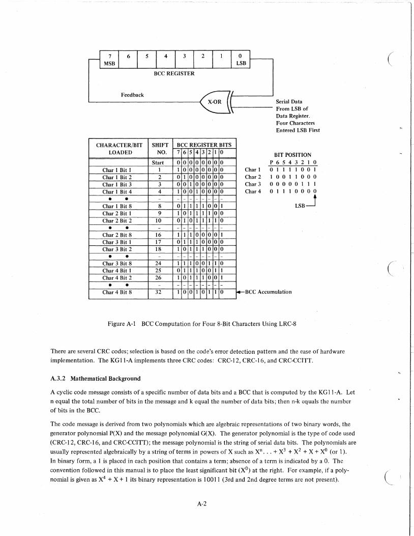
Feedback
CHARACTER/BIT LOADED
Char 1 Bit I Char 1 Bit 2 Char 1 Bit 3 Char 1 Bit 4
• • Char 1 Bit 8 Char 2 Bit I Char 2 Bit 2
• • Char 2 Bit 8 Char 3 Bit 1 Char 3 Bit 2
• • Char 3 Bit 8 Char 4 Bit I Char 4 Bit 2
• • Char 4 Bit 8
BCC REGISTER
SHIFT NO.
Start 1 2 3 4 -8 9
10 -
16 17 18 -
24 25 26 -
32
Serial Data \------ From LSB of
---~
BCC REGISTER BITS 76 5 4 3 2 1 0
o 0 o 0 o 0 o 0 1 0 o 0 o 0 o 0 o 1 o 0 o 0 00 o 0 1 0 o 0 00 I 0 o 1 00 o 0 - - - - - - - -
o I 1 1 1 0 o I I 0 1 1 1 1 o 0 o I o 1 1 1 I 0 - - - - - - - -1 1 1 00 o 0 I o 1 1 I 00 00 I 0 1 1 1 0 o 0 - - - - - - - -1 1 1 o 0 1 1 0 o I 1 1 o 0 1 1 1 011 1 0 o I - - - - - - - -
1 o 0 I 0 110 I+-
Char 1 Char 2 Char 3 Char 4
Data Register. Four Characters Entered LSB First
BIT POSITION P 6 5 4 3 2 1 0 01111001 10011000 o 0 0 0 0 1 1 1 o 1 I 1 0 0 0 0
LSB~
BCC Accumulation
Figure A-I BCC Computation for Four 8-Bit Characters Using LRC-8
There are several CRC codes; selection is based on the code's error detection pattern and the ease of hardware
implementation. The KGll-A implements three CRC codes: CRC-12, CRC-16, and CRC-CCITT.
A.3.2 Mathematical Background
A cyclic code message consists of a specific number of data bits and a BCC that is computed by the KG II-A. Let
n equid the total number of bits in the message and k equal the number of data bits; then n-k equals the number
of bits in the BCC.
The code message is derived from two polynomials which are algebraic representations of two binary words, the
generator polynomial P(X) and the message polynomial G(X). The generator polynomial is the type of code used
(CRC-12, CRC-16, and CRC-CCITT); the message polynomial is the string of serial data bits. The polynomials are
usually represented algebraically by a string of terms in powers of X such as Xn ... + X3 + X2 + X + XO (or I).
In binary form, a 1 is placed in each position that contains a term; absence of a term is indicated by a O. The
convention followed in this manual is to place the least significant bit (Xo) at the right. For example, if a poly
nomial is given as X4 + X + 1 its binary representation is 10011 (3rd and 2nd degree terms are not present).
A-2
(

(
(
Given a message polynomial G(X) and a generator polynomial P(X), the objective is to construct a code message
polynomial F(X) that is evenly divisible by P(X). It is accomplished as follows:
a. Multiply the message G(X) by Xn -k where n-k is the number of bits in the BCC.
b. The resulting product Xn-k [G(X)] is divided by the generator polynomial P(X).
c. The quotient is disregarded and the remainder C(X) is added to the product to yield the code message polynomial F(X), which is represented as Xn -k [G(X)] + C(X).
The division is performed in binary without carries or borrows. In this case, the remainder is always one bit less
than the divisor. The remainder is the BCC and the divisor is the generator polynomial; therefore, the bit length
of the BCC is always one less than the number of bits in the generator polynomial.
A simple example is explained below.
I. Given:
Message polynomial G(X) = 1100 II (X5 + X4 + X + Xo) Generator polynomial P(X) = 1100 I (X4 + X3 + 1)
G(X) contains 6 data bits P(X) contains 5 bits and will yield a BCC with 4 bits; therefore, n-k = 4.
2. Multiplying the message G(X) by Xn -k gives:
Xn -k [G(X)] = X4 (X5 + X4 + X + Xo) = X9 + X8 + X5 + X4
The binary equivalent of this product contains 10 bits and is 1100 110000.
3. This product is divided by P(X)
P(X)-IIOOI
10000 1 - quotient
1100110000- xn-k [G(X)]
11001
10000
11001
100 I _ remainder = C(X) = BCC
4. The remainder C(X) is added to Xn-k [G(X)] to give F(X) = 1100 111001.
The code message polynomial is transmitted. The receiving station divides it by the same generator polynomial.
If there is no error, the division will produce no remainder and it is assumed that the message is correct. A
remainder indicates an error. The division is shown below.
P(X)-IIOOI
100001
1100111001- F(X)
11001
11001
11001
00000 - no remainder
A more practical example of generating a BCC by long division is shown in Figure A-2.
A-3

11000000000000101
Generator Polynomial CRC-16 Xl6 + XiS + X2 + 1
Exclusive-OR Operation
I Quotient (To Be Discarded)
~1111111111111101 10000000000000000000000000000000
11000000000000101 4 10000000000001010 Message (16 Bits) 11000000000000101 Plus 16 Zeros 10000000000011110 11000000000000101
(
10000000000110110 11000000000000101
10000000001100110 11000000000000101
10000000011000110 11000000000000101
10000000110000110 11000000000000101
10000001100000110 ·11000000000000101
10000011000000110 11000000000000101 . 1000011 0000000 11 0
11000000000000101 10001100000000110 11000000000000101
10011000000000110 11000000000000101
10110000000000110 11000000000000101 11100000000000110 11000000000000101
10000000000001100 11000000000000101
Remainder is BCC -~---..,.._ .. 1000000000001001 L MSB
Figure A-2 BCC Computation Using Long Division Method
With CRC-16 as Generator
A.3.3 Hardware Implementation of CRC
The BCC is computed and accumulated in a shift register. The configuration of the register is based on the CRC
code to be implemented. The number of stages in the register is equal to the degree of the generating polynomial;
the number of exclusive-OR elements is a function of the polynomial also. In the subsequent examples, a unique
register configuration is shown for each CRC code (CRC-12, CRC-16, and CRC-CCITT). In the KG II-A, only
one BCe register is used. Logic is used to configure the register for the selected CRe code.
A-4
(
(

c
l
1. CRC-12
2.
3.
CRC-12 is applied to synchronous systems that use 6-bit characters. The BCC accumulation is 12 bits. The generator polynomial is X12 + Xll + X3 + X2 + X + 1 with prime factors of (X+ 1) and (Xll + X2 + 1). It provides error detection of bursts up to 12 bits in length. Additionally, 99.955% of error bursts greater than 12 bits can be detected.
Figure A-3 shows a block diagram configuration of a BCC register for use with CRC-12. A step-by-step shift pattern is shown as the datais serially applied to the register. Initially, the register contains all as. A 12-bit data word (a 1 followed by eleven as is the input to the register). Prior to the first shift, the first data bit (LSB), which is ai, is exclusive-oRed with the a from the LSB of the register. The result on the serial qliotientline is a 1 which is sent via the feedback paths to the following places: bit 11 and the exclusive-ORs between bits 11 and 10, bits 10 and 9, bits 9 and 8, and bits 1 and O. When the feedback settles down, the first shift takes place and produces the register states in the line labeled 1 under the SHIFT NO. column. The shift also presents the next data bit to the input. The process repeats until all 12 data bits are encoded. The BCC is the contents of the register after shift number 12. The most important fact to remember is that the exclusive-OR of tJ:le LSB of the BCC register and the input data bit set up the feedback path prior to the shifting operation. The result of this operation is shown under the column labeled FEEDBACK BEFORE SHIFT. When the shift takes place, the results of the
. exclusive-OR operations are shifted into the register.
The subsequent examples, which show the BCC accumulation for CRC-CCITT and CRC-16, can be analyzed the same way; the register length, data word length, and feedback paths are different but the process is the same.
CRC-CCITT
CRC-CCITT is the standard used to compute a BCC for European systems. When operating with 8-bit characters, the BCC accumulation is 16 bits. The generator polynomial is X16 + X12 + X5 + 1. It provides error detection of bursts up to 16 bits in length.
Figure A-4 shows a BCC accumulation using a 16-bit data word (a 1 followed by fifteen as).
CRC-16
CRC-16 is applied to synchronous systems that use 8-bit characters. The BCC accumulation is 16 bits. The generator polynomial is X16 + X15 + X2 + 1 with prime factors of (X+ 1) and (X15 + X + 1). It provides error detection of bursts up to 16 bits in length. Additionally, 99.955% of error bursts greater than 16 bits can be detected.
Figure A-5 shows a BCC accumulation using a 16-bit data word (a 1 followed by. fifteen as).
The three CRC examples (Figures A-3, A4, and A-5) show BCC accumulations that are to be used in a transmission sequence. Figure A-6 shows the BCC accumulation performed on a message that has been received along with a BCC. The message and the computed BCC have been taken from Figure A-5; i.e., a BCC accumulation using CRC" 16. In Figure A-6, the accumulation process is the same as that shown in Figure A-5 through shift number 16. Starting with shift number 17, the BCC is sent to the data input, LSB first. A correct transmitted BCC results in all as in the BCC register at the end of the computation. In effect, this is a comparison of the transmitted BCC with the one computed at the receiving station. A correct comparison yields a a remainder, or all as in the BCC register.
A.4 HARDWARE CONFIGURATION OF BCC REGISTER
The KG ll-A uses one register to accumulate the BCC for two LRC modes and three CRC modes. It isa 16-bit
register that uses a logic network to provide the proper feedback path and exclusive-OR operators for the LRC or
CRC mode selected. Figure A-7 is a block diagram of the BCC register that shows the configuration for the two
LRC modes and three CRC modes.
A-5

SERIAL QUOTIENT
I--X.3++i'~-'-""""r-T---r-'-T""""'II--~~ 0 X12 ~ BCC REGISTER LSB FEEDBACK MSB
DATA BEFORE
SHIFT NO.
INPUT
Start 0 0 0 0 0 0 0 0 0 0 0 O~ - ~1
1 1 10000000 11--""'1"""--1
2 1 0 0 01000000 1 I 0IB 1
43 1 0 1 1 0 1 0 0 0 0 0 .1 00 .1 11 o 0 1 0 1 00 0 0
5 0 0 0 1 0 1 000 1 1 0 I 1
6 0 0 00 1 0 1 .0 0 1 I 0 I 1 7 0 0 0 0 0 1 010 0 1 8 0 00000101 I 0 I 1
9 0 0000001.0 0 1 0 1 0
10 0 1 0 1 0 0 0 0 0 0 1 0 I 0 1 0 11 0 0 1 0 1 0 0 0 0 0 0 1 0 1
SHIFT
Arrows Indicate Exclusiv.e-OR of Data Bit and LSB of BCC Register Prior to Shift
12 rll~~~I~~~~~-0-0~1-0-0~0-0-0~~~1~0~1
[BlOCk Check Character (BCC) L 12 Bit Data Word
NOTES
o = BCC Register Stage
EB = Exclusive-OR CRC-l2 Polynomial = X 12' + Xll + X3 + X2 + X + 1
Figure A-3 BCC Accumulation Using CRC-12, Transmit Sequence
A-6
(
..

(
Co'
MSB
SHIFT
NO.
Start 0 0 0 0 0 1 000 0
20100 0 3 0 0 1 00 4 000 1 0 5 10001 6 0 10 0 0 700 1 0 0 8 000 1 0 9 1 000 1
10 0 1 0 0 0 11 00100 12 10010 13 1 1 0 0 1 14 0 1 1 0 0 15 0 0 1 1 0 16 10 0 0 1
NOTES
o = BCC Register Stage
€9 = Exc1usive-OR
SERIAL QUOTIENT
BCC REGISTER
0000000 1 0 0 0 0 0 0 o 1 0 0 0 0 0 001 0 0 0 0 o 00 1 0 0 0 100 0 1 0 0 1 1 000 1 0 o 1 1 000 1 001 1 000 100 1 100 1 10 0 1 1 0 o 1 100 1 1
o 1 100 1
0000--.....-~1 1000 1 1 LSB O
0100 1 00 1 00 001 0 0001 1 0 1 1
1000 I 0 1 0
0100 1 0 1 0
0010 1 00 1 0 10011 1 1 0 0 10 1 0
0110 10 10 o 0 1 1 0 1
0001101 1 101 100 0 0 0 0 100 -1 11 0 1 1 0 00 0 0 1 0 : 0 o 1 1 101 1 0 0 0 0 0 0
LSB
DATA BEFORE
INPUT SHIFT
Arrows Indicate
Exc1usive-OR
of Data Bit , and LSB of
BCC Register
Prior to Shift
0011101 1000f-..0~0 -L Block Check Character (BCC) L 16 Bit Data Word
CRC-CCITT Polynomial = X16 + X12 + X5 + 1
Figure A-4 BCC Accumulation Using CRC-CCITT, Transmit Sequence
A-7

MSB
SHIFT NO.
SERIAL QUOTIENT
BCC REGISTER
Start 0 0 0 0 0 0 0 0 0 0 0 0 0 0 0 0 - 1
1 10 1000000000000 1~1~1 2 1100000000000 1 1 0 11 34 11 0110000000000 1 00 111
o 0 1 1 0 0 0 0 00 0 0 0
5 0 0 0 1 1 0 00 0 0 0 0 0 I 0 I 6 0000110000000 I 0 I 78 0000011000000 I 00 I
o 0 0 0 0 0 1 100 0 0 0 9 0000000110000 I 0 I
10 0 0 0 0 0 0 0 0 1 1 0 0 01 0 I 112i 0 0 0 0 0 0 0 0 0 1 1 0 0 I 00 I
o 0 0 0 0 0 0 000 1 1 0
13 0000000000011 I 0 I 14 0 0 0 0 0 0 0 0 0 0 0 0 1 0 I 0 I 0 15 0 1 1 0 0 0 0 0 0 0 0 0 0 0 0 l~ 0 ............... 1
DATA BEFORE INPUT SHIFT
Arrows Indicate Exclusive-OR of Data Bit and LSB of BCC Register Prior to Shift
16 r-I 1-0----0-1-0-0-0-0 -0-0--0-0--0-0--0----:-1 I 0 MSB 1
L Block Check Character (BCC) t..== 16 Bit Data Word
NOTES D = BCC Register Stage E9 = Exclusive-OR
CRC-16 Polynomial = XI6 + XIS + X2 + 1
Figure A-S BCC Accumulation Using CQ.C-16, Transmit Sequence
A-8
(
(
(

(
C
SERIAL QUOTIENT
MSB BCC REGISTER
SHIFT NO.
Start o 0 000 0 0 0 0 0 000 0 0 1 0 100 000 0 000 000
2 1 1 1 1 000 0 0 0 0 000 0 3 1 1 o 1 1 .0 0 0 0 0 0 0 0 0 0 4 1 1 00 1 1 00 0 0 0 0 0 0 0
• • • • • • • • • Same as CRC-16 Transmit •
• • • • Sequence (See Figure A-5) •
• • • • • 13 1 1 0000000 0 000 1 1 14 1 1 o 0 0 0 0 0 0 0 0 0 001 15 o 1 1 000 0 0 0 0 0 0 0 0 0 16 11 0 o 1 0 0 0 0 000 0 0 0 0 17 o 1 o 0 1 0 0 0 0 0 0 0 000 18 o 0 100 1 0 0 0 000 0 0 0 19 o 0 o 1 001 0 0 0 0 0 0 0 0 20 00 00100 1 0 0 0 000 0 21 00 000 1 001 0 0 0 0 0 0 22 00 000 0 1 001 0 0 0 0 0 23 00 00000 1 001 0 0 0 0 24 00 o 0 0 0 0 0 1 001 000 25 00 o 0 0 0 0 001 001 0 0 26 o 0 000 000 0 0 1 001 0 27 o 0 o 0 0 000 0 001 001 28 o 0 o 0 0 0 0 0 0 000 1 0 0 29 o 0 000 0 000 0 000 1 0 30 o 0 000 000 0 0 0 0 0 0 1 31 o 0 o 0 0 0 0 0 0 0 0 000 0 32 @:O o 0 0 0 0 0 0 0 0 0 0 0 0
BCC Register ALL Os Received Message Assumed To Be Correct
NOTES o = BCC Register Stage €a = Exclusive-OR
CRC-16 Polynomial = X16 + X15 + X2 + 1
X16
4FEE~ACK 0 LSB
DATA BEFORE INPUT SHIFT
0----.... - 1 1 1<.1 1 0 1 Arrows Indicate 1 0 1 Exclusive-OR
1 0 of Data Bit
• • • and LSB of
• • • BCC Register DATA • • • Prior to Shift
• • • 0
0 0 0 0 0 MSB
0 1 LSB 0 0 0 \ 0
0 0 0 0 0 0 0 0 0 0 0 0 0 0 0 0 0 BCC 0 0 0 0 0 0 0 0 0 0
0 0 0 0 0 0 0
1;--...0~0 o 1 MSB 0 46 Bit ""ta Won!
and BCC Received
Figure A-6 BCC Accumulation Using CRC-16, Receive Sequence
A-9

(
LR~ 7 6 QUO
NOTES:
1. Each Bee Register stage (Flip Flop) shown as a numbered box.
2. EB = Exclusive OR.
3. Data Flow is Left to Right.
11-0923
Figure A-7 Bee Register, Block Diagram
A-lO

(
( "
APPENDIX B
ABBREVIATIONS
This appendix contains two abbreviation lists. List I contains abbreviations that are used throughout the manual.
List 2 contains the USASCII control characters used in the message examples in Chapter 4.
BCC BG CCITT CLK CLR CRC CSR DATI DATO DATOB DDB H INIT L LRC LSB MSB QUO REG SEL SEN USASCII VRC X-OR
DLE ETB ETX ITB STX
List 1 - Abbreviations
block check character bus grant Consultative Committee for International Telephone and Telegraph clock clear cyclic redundancy check control and status register data in data out data out, byte double data byte high initialize low longitudinal redundancy check least-significant bit most -significant bit quotient register select shift-enable USA Standard Code for Information Interchange vertical redundancy check exclusive-OR
List 2 - USASCII Control Characters
Data Link Escape End of Transmission Block End of Text Intermediate Block Check Character Start of Text
B-1

(
(:
APPENDIX C
INTEGRATED CIRCUIT DESCRIPTIONS
This appendix provides a description, pin designation diagram, logic diagram, and truth table for the more
complex integrated circuits (lCs) used in the KGII-A. They are listed below.
7474 Dual D-Type Edge-Triggered Flip-Flops 8242 4-Bit Digital Comparator 8266 2-Input 4-Bit Digital Multiplexer 8271 4-Bit Shift Register 74197 Presettable Binary Counter/Latch
All but the 7474 are categorized as medium scale integration (MSI) devices.
C-I

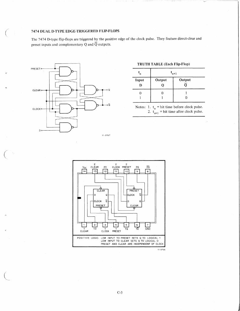
c
""
(
7474 DUAL D-TYPE EDGE-TRIGGERED FLIP-FLOPS
The 7474 D-type flip-flops are triggered by the positive edge of the clock pulse. They feature direct-clear and
preset inputs and complementary Q and Q outputs.
PRESET
CLEAR
CLOCK
Do-------l
TRUTH TABLE (Each Flip-Flop)
tn tn+l
Input Output Output
0 Q Q 0
0 0 0
Q Notes: 1. tn = bit time before clock pulse.
2.
11-0767
2 2 2 Vee CLEAR 2D CLOCK PRESET 20 2c5
1
1 CLEAR
CLEAR PRESET
D 0 CLOCK Q
CLOCK Q D 0
CLEAR
1 1 10 fo GND CLOCK PRESET
tn+l = bit time after clock pulse.
POSITIVE LOGIC: LOW INPUT TO PRESET SETS 0 TO LOGICAL 1 LOW INPUT TO CLEAR SETS 0 TO LOGICAL 0 PRESET AND CLEAR ARE INDEPENDENT OF CLOCK
11-0766
C-3


(
(- \
"
-q-.:
c
---~------- ------ --- -- -- ---- - - -- ------ ---------- ----- -- --- --- ----" ... -------"-- -------"--- - - - --------------
8242 4-BIT DIGITAL COMPARATOR (QUAD EXCLUSIVE-NOR)
The 8242 contains four independent exclusive-NOR gates which may be used to implement digital comparison
functions. The 8242 outputs are bare collector to facilitate implementation of multiple-bit comparisons; a 4-bit
comparison is made by connecting the outputs of the four independent gates together. This common output
connection is high only when all input pairs are matched (both as or both 1 s).
14 13 12 11 10 9 8
1234567
AO BO AI Bl A2 B2 A3 B3
I l A B , 0 0 1 1 0 0 0 1 0 1 1 1
I I I I I I I I I I
TRUTH TABLE
I I I I L_ _-.J
'0 'I '2 '3
11-0472
C-5


(
C
.01;',
8266 2-INPUT 4-BIT DIGITAL MULTIPLEXER
The 8266 multiplexer is able to choose from two different input sources, each containing 4 bits:
A = (AO' AI' A2, A3), B = (BO' B1, B2 , B3). The selection is controlled by input SO' while the second control
input, SI' is held at O.
16 15 1413 12"11 10 9
12345678 II·048S
.------I I I
50
51
I I I L ______
AO 8 0
Fa
C-7
TRUTH TABLE
AI
Select Lines
So SI
o o
Bl A2
o 1 o
- --
Fl F2
Output
fn (0,1,2,3)
B2 A3 B3
-, I I I I I I I I
_...J
F3
11-0479


(
-
(
~
8271 4-BIT SHIFT REGISTER
The 8271 is a 4-bit shift register with both serial and parallel data entry capability. The data input lines are
single-ended true input data lines which condition their specific register bit location after an enabled clocking
transition. Since data transfer is synchronous with the clock, data maybe transferred in any serial/parallel input/
output relationship.
The internal design uses stored charge binaries to effect a desirable speed/power relationship. These binaries
respond to the negative-going clock transition. A buffer clock driver has been included to minimize input clock
loading and reduce the input clock transition requirements.
Mode control logic is available to determine three possible control states: serial shift right mode, parallel enter
mode, and no change or hold mode. These states accomplish logical decoding for system control. The truth table
for the control modes is shown below. For applications not requiring the hold mode, the load input may be tied
high and the shift input used as the mode control.
The 8271 provides a direct reset (RD), and a Dout line.
16 15 14 13 12 11 10 9
Vee Oc DD SHIFT DOUT DOUT LOAD COUT
GND
2 3 4 5 6 7 8
12-0322
TRUTH TABLE
Control State Load Shift
Hold 0 0 Parallel Entry I 0 Shift Right 0 Shift Right
C-9

-----0,8 ~~----------------------~~--------~~
O'n-~ _________ ~ o
u.o--I--l-------1 o
~~~~--------------I --L-----;;;;o
O~~~---------~ < -J __ ------~~
ColO
... N
" ~ (
c
"

(
(
74197 PRESETTABLE BINARY COUNTER/LATCH
This high-speed monolithic counter consists of four dc-coupled master-slave flip-flops which are internally inter
connected to provide a divide-by-2 counter and a divide-by-8 counter. This counter is fully programmable; i.e.,
the outputs may be preset to any state by placing a low on the count/load input and entering the desired data at
the data inputs. The outputs change to agree with the data inputs independent of the state of the clocks.
The counter may also be used as a 4-bit latch by using the count/load input as the strobe and entering data at the
data inputs. The outputs directly follow the data inputs when the count/load input is low, but remain unchanged
when the count/load input is high and the clock inputs are inactive.
As a high-speed counter, the 74197 accepts count frequencies of 0 to 50 MHz at the clock-l input and 0 to
25 MHz at the clock-2 input. During the count operation, transfer of information to the outputs occurs on the
negative-going edge of the clock pulse .. This counter features a direct-clear which, when taken low, sets all outputs
low regardless of the states of the clocks.
The output of flip-flop A is not internally connected to the succeeding flip-flops; therefore, the counter may be
operated in two independent modes:
I. When used as a high-speed 4-bit ripple-through counter, output QA must be externally connected to the clock-2 input. The input count pulses are applied to the clock-l input. Simultaneous divisions by 2, 4,8, and 16 are performed at the QA' QB' and Qn outputs.
2. When used as a 3-bitripple-through counter, the input count pulses are applied to the clock-2 input. Simultaneous frequency divisions by 2, 4, and 8 are available at the QB' Qc' and Qn outputs. Independent use of flip-flop A is available if the load and cle.ar functions coincide with those of the 3-bit ripplethrough counter.
DATA INPUTS . CLOCK
Vee CLEAR QD D S QS 1
C A CLOCK GND , 2 DATA INPUTS
ASYNCRONOUS INPUT, LOW INPUT TO CLEAR SETS QA Qs, Qc AND QD LOW.
"Pin assignments for these circuit. are 1he same for all packages.
11·0482
C-ll

DATA A 0------------1
COUNT/LOAD o----Q
CLEAR o-..... --____l PRESET
QA
CLOCK1 0---------+-~----_4-----~ T
DATA B o--~~-----+____l~
-CLOCK 2 0---------+-1------1------01 T
DATA C
PRESET
QC QC
DATA D 0---------+-1--1
C-12
T
PRESET
QD
T
11-0481
(
f.'
(
(1

(
(
(~
---- ---~--- -----------~--- - ---------------~- -----~------ ~-- ---- -~---------
READER'S COMMENTS
--------------------------------c~=~-~-_C----=---=-==============,
KGll-A EXCLUSIVE-OR and CRC BLOCK CHECK MANUAL DEC-II-UKGAB-A-D
Y04,r comments and suggestions will help us in our continuous effort to improve the quality and usefulness of
our publications.
What is your general reaction to this manual? In your judgment is it complete, accurate, well organized, well
written, etc.? Is it easy to use?
What features are most useful? --------------------------------------------------------
What faults do you find with the manual? ________________________ _
Does this manual satisfy the need you think it was intended to satisfy? _______________ _
Does it satisfy your needs? Why? _______________________________ __
Would you please indicate any factual errors you have found.
Please describe your position.
Name ___________________ __ ~gan~ation ________________ __
Street _~--------------- Department
City -'--_______________ ~ State _____ ...,-__________ ..,--_ Zip qr Country ______ _
- - - - - - - - - - - - - - - - - - Fold Here - - - - - - - - - - - - - - - - - - - - -
- - - - - - - - - - - - - - Do Not Tear· Fold Here and Staple - - - - - - - - - - - - -
BUSINESS REPLY MAIL
NO POSTAGE STAMP NECESSARY IF MAilED IN THE UNITED STAn'S
Postage ,,"11 be paid by:
Digital Equipment Corpor~tion Technical Documentation Department 146 Main Street Maynard, Massachusetts 01754
FIRST CLASS
PERMIT NO. 33
MA YNARD. MASS.
(


DIGITAL EQUIPMENT CORPORATION MAYNARD, MASSACHUSETTS 01754