
Kent Academic Repository - University of Kent Fabrication of Frequency... · for further reuse of...
206
Kent Academic Repository Full text document (pdf) Copyright & reuse Content in the Kent Academic Repository is made available for research purposes. Unless otherwise stated all content is protected by copyright and in the absence of an open licence (eg Creative Commons), permissions for further reuse of content should be sought from the publisher, author or other copyright holder. Versions of research The version in the Kent Academic Repository may differ from the final published version. Users are advised to check http://kar.kent.ac.uk for the status of the paper. Users should always cite the published version of record. Enquiries For any further enquiries regarding the licence status of this document, please contact: [email protected] If you believe this document infringes copyright then please contact the KAR admin team with the take-down information provided at http://kar.kent.ac.uk/contact.html Citation for published version Turki, Badredin (2015) Digital Fabrication of Frequency Selective Surfaces for In-Building Applications Using Inkjet Printing Technology. Doctor of Philosophy (PhD) thesis, University of Kent,. DOI Link to record in KAR http://kar.kent.ac.uk/56652/ Document Version UNSPECIFIED
-
Upload
truongnguyet -
Category
Documents
-
view
213 -
download
0
Transcript of Kent Academic Repository - University of Kent Fabrication of Frequency... · for further reuse of...

Kent Academic RepositoryFull text document (pdf)
Copyright & reuse
Content in the Kent Academic Repository is made available for research purposes. Unless otherwise stated all
content is protected by copyright and in the absence of an open licence (eg Creative Commons), permissions
for further reuse of content should be sought from the publisher, author or other copyright holder.
Versions of research
The version in the Kent Academic Repository may differ from the final published version.
Users are advised to check http://kar.kent.ac.uk for the status of the paper. Users should always cite the
published version of record.
Enquiries
For any further enquiries regarding the licence status of this document, please contact:
If you believe this document infringes copyright then please contact the KAR admin team with the take-down
information provided at http://kar.kent.ac.uk/contact.html
Citation for published version
Turki, Badredin (2015) Digital Fabrication of Frequency Selective Surfaces for In-Building ApplicationsUsing Inkjet Printing Technology. Doctor of Philosophy (PhD) thesis, University of Kent,.
DOI
Link to record in KAR
http://kar.kent.ac.uk/56652/
Document Version
UNSPECIFIED

Digital Fabrication of Frequency Selective Surfaces for In-Building Applications
Using Inkjet Printing Technology
A Thesis Submitted to The University of Kent for the Degree of Doctor of Philosophy
in Electronic Engineering
By Badredin M. Turki

To My Parents Mohamed & Nadia

Abstract
This thesis presents work on the inkjet printing manufacture of frequency selective
surfaces intended for in-building applications using silver nanoparticle inks. The aim
of this research is to investigate the performance of inkjet printed FSS panels in terms
of transmission response, element conductivity, and the resolution of the printed lines,
all of which are produced efficiently in terms of cost and resource usage. Different
FSS design were investigated from simple elements such as linear dipoles, square
loops and convoluted square loop elements.
Various techniques were used in the manufacturing process such as different ink drop
spacing, number of jetted ink layers, and different sintering methods, with the aim of
achieving low cost manufacturing with a reduced amount of deposited silver inks and
sintering time and temperature. Additionally, further reductions in the deposited ink
were considered by the introduction of frame elements.
The research also focuses on factors that could affect the transmittivity/reflectivity of
the FSS screen, such as the influence of imperfections in the printed elements. The
imperfections are expected in the case of low cost mass production, therefore it is
important to understand to what extent they could be tolerated whilst still providing
adequate performance.
Finally, the work also considers developing novel slotted FSS arrays operating at low
frequency bands such as the TETRA emergency band and suitable for additive
manufacturing.
Badredin Turki
December 2015

Acknowledgment
Firstly, I am extremely grateful to my supervisor Prof. John C. Batchelor for his
valuable advice and support of all means through the difficulties I experienced during
my PhD studies. I also would like to show the deepest gratitude to my advisor
Prof. Edward A. (Ted) Parker for his guidance and support which greatly inspired and
improved my research all throughout the PhD. Following, I would like to thank
Mr. Richard Douglas from the Income office for his time, trust and patience; it is also
through his support that I have been able to complete my studies.
Secondly, I would like to thank the Leche Trust for their grant and generosity which
provided me precious support in the final phase. Thanks to both Mr. Simon Jakes and
Mr. Antonio Mendoza for their excellent assistance and efforts on measurements and
mechanical aspects. I also thank Dr. Ali Ziai and Dr. Benito Sanz Izquierdo for their
help and advice on the subject of frequency selective surfaces, measurements and
simulations. Special thank you to Prof. Stephen Yeates and Dr. Rachel Saunders from
the OMIC at the University of Manchester for their support in providing the inkjet
printed FSS samples. Furthermore, I would like to thank Mr. Steve Thomas and
Mr. Julian Shilton from CIT Technology for the electroless copper plated FSS
samples. Thanks also to all members of staff in the School of Engineering for their
professionality and hard work.
I want to show special appreciation to Valeria Boron whose unrelenting support and
encouragement thorough out the duration of my PhD helped me to get through the
tough times. Also I would like to acknowledge in a special way Mr. Dumtoochukwu
Oyeka, Dr. Osman Rakibet, Dr. Srijittra (Note) Swaisaenyakorn, Mr. Samir Malik and
Dr. Eleni Dimou for their support, motivation and advice throughout my PhD.
Finally I would like to truly thank my parents (Mohamed and Nadia), brothers and
sisters for being supportive, encouraging and understanding throughout my studies in
the UK without which I couldn’t have attained the successful completion of this work.

I
CONTENTS Chapter 1: Introduction ................................................................................................ 1
1.1 Overview and Motivations ................................................................................. 1
1.2 Research Objectives and Contributions.............................................................. 2
1.2.1 Objectives .................................................................................................... 2
1.2.2 Contributions ............................................................................................... 3
1.3 Thesis Outline ..................................................................................................... 3
1.4 Publications arising from this work .................................................................... 5
References ................................................................................................................ 7
Chapter 2: Frequency Selective Surfaces A Review of Literature .............................. 8
2.1 Introduction ........................................................................................................ 8
2.2 Important factors in FSS design ....................................................................... 12
2.2.1 Types of FSS .............................................................................................. 12
2.2.2 Angle of incidence ..................................................................................... 15
2.2.3 Grating response ........................................................................................ 16
2.3.4 Influence of the supporting dielectric substrate ......................................... 17
2.2.5 Convoluted elements.................................................................................. 20
2.3 FSS in buildings ............................................................................................... 23
2.4 Summary .......................................................................................................... 27
References .............................................................................................................. 28
Chapter 3: Frequency Selective Surfaces Panels - Fabrication and Measurements ... 32
3.1 Introduction ...................................................................................................... 32
3.2 Inkjet Printing Technology ............................................................................... 32
3.2.1 Technology Overview................................................................................ 32
3.2.2 Printing process.......................................................................................... 34
3.2.3 Defects in the printed structures ................................................................ 40
3.3 FSS screen fabrication ...................................................................................... 42
3.3.1 Inkjet printing of FSS screens .................................................................... 42
3.3.2 Chemical etching of FSS screens............................................................... 46
3.4 FSS Measurement set up .................................................................................. 47
3.5 FSS Modelling and Simulations ....................................................................... 49
3.6 Summary .......................................................................................................... 52
References .............................................................................................................. 53

II
Chapter 4: Study of the Impact of Defects on the Performance of FSS Panels ......... 58
4.1 Introduction ...................................................................................................... 58
4.2 Randomly (Arbitrarily) missing elements ........................................................ 60
4.2.1 Skewed lattice dipole arrays ...................................................................... 60
4.2.2 Square lattice dipole arrays ........................................................................ 63
4.2.3 Square loop arrays ..................................................................................... 63
4.2.4 Ring loop arrays ......................................................................................... 64
4.3 Clusters of elements ......................................................................................... 65
4.4 Measurements and simulation results ............................................................... 67
4.4.1 Randomly missing and defective elements ................................................ 67
4.4.2 Clusters of missing elements ..................................................................... 74
4.4.3 Clustering a metal sheet ............................................................................. 78
4.5 Illumination ...................................................................................................... 80
4.5.1 Removing 20% of elements at random locations ...................................... 80
4.5.2 Changing the antenna beam position ......................................................... 81
4.5.3 Oblique angel of incidence ........................................................................ 85
4.6 Conclusion ........................................................................................................ 87
References .............................................................................................................. 89
Chapter 5: Inkjet Printing of Solid and Frame Dipole Element Frequency Selective Panels ......................................................................................................................... 91
5.1 Introduction ...................................................................................................... 91
5.2 FSS design and manufacturing parameters ...................................................... 93
5.2.1 Thermal sintering ....................................................................................... 94
5.2.2 Plasma and photonic sintering of FSS arrays ............................................ 98
5.3 Inkjet printing of FSS panels on PEL paper ................................................... 101
5.3.1 Inkjet printing of solid dipole elements ................................................... 101
5.3.2 Frame dipole elements ............................................................................. 103
5.3.3 Superimposed solid dipole elements........................................................ 108
5.4 Printing defects ............................................................................................... 110
5.5 Dimensions of the inkjet printed panels ......................................................... 116
5.6 Resistance study ............................................................................................. 119
5.7 Conclusion ...................................................................................................... 125
References ............................................................................................................ 127
Chapter 6: Inkjet Printing of Convoluted FSS Elements ......................................... 130
6.1 Introduction .................................................................................................... 130

III
6.2 FSS designs .................................................................................................... 132
6.2.1 Angular stability ...................................................................................... 134
6.3 Inkjet fabrication of FSS arrays ...................................................................... 136
6.3.1 Square loops ............................................................................................. 136
6.3.2 Inkjet printed Semi-convoluted Square element (Maltese cross) FSS arrays ................................................................................................................. 141
6.3.3 Inkjet printed Convoluted Square elements FSS arrays .......................... 143
6.4 Inkjet printed square elements with Silverjet Ink ........................................... 145
6.5 Inkjet printed convoluted square elements with Silverjet Ink ........................ 148
6.6 Inkjet printed square elements slot arrays with Silverjet Ink ......................... 153
6.7 Conclusion ...................................................................................................... 156
References ............................................................................................................ 158
Chapter 7: FSS Manufacture by Electroless Copper Plating on an Inkjet Printed Catalyst ..................................................................................................................... 161
7.1 Introduction .................................................................................................... 161
7.2 Skewed lattice dipole FSS arrays ................................................................... 163
7.3 Convoluted square element FSS arrays .......................................................... 166
7.4 Interwoven square loop slots FSS panel ......................................................... 169
7.5 Densely convoluted slotted (DCS) cross dipole elements FSS arrays ........... 171
7.6 Conclusion ...................................................................................................... 177
References ............................................................................................................ 179
Chapter 8: Conclusions and Future Work ................................................................ 181
8.1 Conclusions .................................................................................................... 182
8.2 Future Work ................................................................................................... 187

IV
L IST OF FIGURES Fig. 2. 1 Square loop elements ..................................................................................... 9
Fig. 2. 2 Equivalent circuit model and transmission response of: (a) Square loop, (b)
Double square loop elements ..................................................................................... 10
Fig. 2. 3 FSS arrays filter types with their transmission response: (a) Band stop, (b)
Band pass, (c) Low pass and (d) High pass ............................................................... 11
Fig. 2. 4 Common FSS element types ......................................................................... 13
Fig. 2. 5 Transmission response of linear dipole array with oblique angle of incidence:
(a) TE and (b) TM [27] .............................................................................................. 15
Fig. 2. 6 Effect of dielectric substrate on the resonant frequency fr: (a) infinite
thickness and (b) finite thickness d ............................................................................ 18
Fig. 2. 7 Variation of resonance frequency at normal incidence with dielectric
thickness (d); continuous curves: dipole slots, broken curves: dipole patches [31] . 19
Fig. 2. 8 Examples of convoluted elements; (a) convoluted dipoles [27] (b) Convoluted
cross dipole [33] ........................................................................................................ 20
Fig. 2. 9 Measured transmission response; (a) linear dipole, (b) convoluted dipole
[27] ............................................................................................................................. 21
Fig. 2. 10 Scenarios of FSS applications within a high-rise building (1) Rooms with
secured indoor WLAN and isolated from outside (only allow Emergency TETRA), (2)
Solely secured for indoor WLAN open to outside (TETRA, GSM, DCS, UMTS), (3)
Open Rooms with black spots Requiring improved internal propagation, (4) Enclosed
room (allow Emergency Services) ............................................................................. 23
Fig. 2. 11 Inkjet printed arrays of simple linear silver dipoles on PEN [46] ............ 25
Fig. 2. 12 Measured transmission responses of the inkjet printed and chemically
etched dipole FSS arrays ........................................................................................... 26
Fig. 2. 13 Equivalent circuit model and the transmission response of square loop
elements FSS: in the case of variable conductivity .................................................... 26
Fig. 3. 1 Principles of operation of (a) Continuous inkjet (CIJ) and (b) drop – on –
demand (DOD) inkjet printers [16] ........................................................................... 35
Fig. 3. 2 Inkjet printing process [17] ......................................................................... 36
Fig. 3. 3 Diagram of overlapped neighbouring droplets ........................................... 37

V
Fig. 3. 4 Inkjet printed lines with different drop – spacing: (a) no overlap, (b) minimum
overlap, (c) sufficient overlap, and (d) too large overlap (too small drop spacing [16]
.................................................................................................................................... 38
Fig. 3. 5 Satellite drop effect [34] .............................................................................. 40
Fig. 3. 6 Microscopic images of crack patterns in silver ink printed lines with width of
0.4mm after drying and sintering [35] ....................................................................... 41
Fig. 3. 7 Dimatix DMP-2800 inkjet printer ............................................................... 43
Fig. 3. 8 The absorbing screen ................................................................................... 47
Fig. 3. 9 FSS transmission response measurement setup .......................................... 48
Fig. 3. 10 Modelled finite dipole FSS screen ............................................................. 50
Fig. 3. 11 Simulated transmission responses of square loop FSS arrays (L = 23 mm,
P = 25 mm, w=0.2 mm) ............................................................................................. 51
Fig. 3. 12 Simulated transmission responses of the square loop FSS arrays with
variable conductivities ............................................................................................... 51
Fig. 4.1 The linear dipole FSS [19] ........................................................................... 61
Fig. 4.2 Modelled dipole arrays with missing elements (a) complete, (b) 10% missing,
(c) 20% missing, (d) 30% missing (e) 40% missing .................................................. 62
Fig. 4.3 Skewed lattice dipole arrays with discontinuity in some elements [19] ....... 63
Fig. 4.4 Square lattice dipole FSS [19]...................................................................... 63
Fig. 4.5 Square loop FSS [20] ................................................................................... 64
Fig. 4.6 Ring loops FSS .............................................................................................. 64
Fig. 4.7 Fabricated skewed lattice FSS (P = 10.4 mm) with missing dipole clusters of
(a) 10% at the centre, (b) 20% at the centre, (c) 10% at the corner and (d) 20% at the
corner [21] ................................................................................................................. 66
Fig. 4.8 Transmission responses (S21) of skewed lattice dipole arrays with missing
elements: (a) measured [19], and (b) simulated ................................. 68
Fig. 4.9 Transmission responses (S21) of skewed lattice dipole arrays with
discontinuities: (a) measured [19] and (b) simulated ................................ 70
Fig. 4.10 Measured transmission responses (S21) of different FSS arrays ................ 72
Fig. 4.11 Changes in the square loop arrays resonant frequency (fr) vs. the percentage
of missing elements [20] ............................................................................................ 73
Fig. 4.12 Effect of element absence on the -10 dB bandwidth ................................... 73

VI
Fig. 4.13 Measured transmission responses (S21) clustered skewed lattice dipole FSS
(P=10.4 mm) [21] ...................................................................................................... 74
Fig. 4. 14 Measured transmission responses (S21) clustered skewed lattice dipole FSS
with larger periodicity (P=15.4 mm) [21] ................................................................. 75
Fig. 4.15 Measured transmission responses (S21) clustered square lattice dipole FSS
[21] ............................................................................................................................. 76
Fig. 4.16 Measured transmission responses (S21) square loop FSS arrays ............... 77
Fig. 4.17 Measured transmission responses of the clustered skewed lattice dipole
arrays (30GHz) .......................................................................................................... 77
Fig. 4.18 Measured transmission responses (S21) of clusterd metal sheets ............... 79
Fig. 4.19 Measured transmission responses (S21) square loop FSS arrays ............... 81
Fig. 4.20 Transmitter antenna alignment at the (a) un-clustered corner (b) clustered
corner ......................................................................................................................... 82
Fig. 4.21 Measured transmission responses of the skewed lattice dipole arrays
(P=10.4 mm) when the transmitter antenna aligned to (a) un-clustered corner (b)
clustered corner of the arrays .................................................................................... 83
Fig. 4. 22 Influence of oblique angle of incidence on the measured transmission
responses of square loop arrays (a) perfect arrays (b) arrays with 10% missing
elements (c) arrays with 20% missing elements ........................................................ 86
Fig. 5.1 Inkjet printed dipole elements FSS on PEL substrate................................... 94
Fig. 5.2 Measured transmission responses (at normal incidence) of inkjet printed FSS
arrays with different dot-spacing on tattoo and PEL papers ..................................... 95
Fig. 5.3 Measured transmission responses of inkjet printed FSS arrays with different
sintering time and temperature on PEL papers ......................................................... 96
Fig. 5. 4 Measured sheet resistances of inkjet printed elements with 15, 20 and 25 µm
dot-spacing on tattoo and PEL papers [22] .............................................................. 97
Fig. 5.5 Measured transmission responses of inkjet printed FSS arrays on tattoo and
PEL papers with different sintering; plasma and IPL ............................................... 98
Fig. 5.6 Microscopic images of printed elements on transfer paper (a) and (b), (c) on
PEL Paper [22] .......................................................................................................... 99
Fig. 5.7 Measured sheet resistances of inkjet printed patterns with 15, 20 and 25µm
dot-spacing on PEL papers with plasma sintering [22] .......................................... 100

VII
Fig. 5. 8 Measured transmission responses of the copper etched and 1, 2, 3 layer inkjet
printed FSS panels [27]. .......................................................................................... 101
Fig. 5.9 Effect of various substrate (a) thickness, and (b) permittivity, on the array
resonant frequency. The broken curves show the best fit trends [27] ..................... 102
Fig. 5.10 Surface current induced in (a) solid and (b) frame dipole elements at 12.8
GHz [27] .................................................................................................................. 103
Fig. 5.11 Inkjet printed FSS: frame dipoles ............................................................. 104
Fig. 5.12 Measured transmission responses: inkjet printed Solid and Frame dipole
FSS [27] ................................................................................................................... 105
Fig. 5.13 Measured transmission responses: copper clad etched Solid and Frame
dipole FSS [28] ........................................................................................................ 105
Fig. 5.14 Measured transmission responses of the inkjet fabricated solid dipole FSS
arrays with: 1 and 2 deposited ink layers ................................................................ 106
Fig. 5.15 Measured transmission responses of the inkjet fabricated solid and frame
FSS arrays with: 1 and 2 deposited ink layers ......................................................... 107
Fig. 5.16 The fabrication sequence of superimposed dipole FSS arrays ................. 108
Fig. 5.17 Transmission responses S21 of: 1-layer solid dipoles, 1-layer frame dipoles
are compared with depositing frames on top of pre-deposited dipoles, (a) measured,
and (b) simulated ..................................................................................................... 109
Fig. 5.18 1mm inkjet printed solid dipole FSS (a) 1-layer of deposited ink (b) 2-layer
of deposited ink [27] ............................................................................................ 110
Fig. 5.19 0.2 mm inkjet printed frame dipole FSS (a) 1- layer of deposited ink (b) 2-
layer of deposited ink [27] ....................................................................................... 111
Fig. 5.20 Defective dipole elements: (a) dipole with a slot, (b) dipole with two sprayed
edge lines, (c) dipole with Horizontal gaps and (d) misaligned dipole with horizontal
gaps [29]. ................................................................................................................. 112
Fig. 5.21 Modelled dipole FSS printing errors [29] ............................................... 113
Fig. 5.22 Simulated effect of printing errors in dipole elements on the FSS resonant
frequency [29] .......................................................................................................... 114
Fig. 5.23 Effects of different drop spacing and multiple layer deposition on the width
and height of the printed element profile ................................................................. 116
Fig. 5.24 Microscopic image; difference in the 70µm 2- layers frame element arms
.................................................................................................................................. 117

VIII
Fig. 5.25 Measured transmission responses (a) and resistance values (b) of the 0.4mm
solid and 70µm frame dipole FSS [27] .................................................................... 120
Fig. 5. 26 Measured transmission responses (a) and resistance values (b) of the 1mm
solid and 0.15 and 0.2 mm frame dipole FSS [27] .................................................. 121
Fig. 5.27 Elements average resistance vs. transmission response ........................... 123
Fig. 6.1 FSS panels’ designs: (a) Convoluted Squares, (b) semi-convoluted square
loops (Maltese cross) and (c) simple square loops arrays ...................................... 132
Fig. 6.2 Transmission responses of the FSS arrays: (a) Measured, (b) Simulated.. 133
Fig. 6.3 Transmission responses of the convoluted square FSS arrays with oblique
angle if incidence: (a) Measured, (b) Simulated ...................................................... 134
Fig. 6.4 Measured transmission responses of the inkjet printed and chemically etched
simple square FSS arrays ........................................................................................ 137
Fig. 6.5 Microscopic image of the single layer inkjet printed square loops line
definitions ................................................................................................................. 137
Fig. 6.6 Microscopic images of the inkjet printed square loops vertical line definitions:
(a) single and (b) double ink layers ......................................................................... 139
Fig. 6.7 Illustrates the steps of dc resistance measurement of the inkjet printed square
elements FSS arrays: (a) corner to corner or (loop), (b) horizontal lines and (c)
vertical lines ............................................................................................................. 140
Fig. 6.8 Transmission responses of the inkjet printed and chemically etched Semi-
convoluted FSS arrays ............................................................................................. 141
Fig. 6.9 Microscopic photos of the vertical and diagonal lines of (a) single and (b) 2
layers inkjet printed semi-convoluted elements (Maltese cross) FSS arrays ........... 142
Fig. 6.10 Convoluted square elements arrays: (a) 0.2 and 0.4 mm chemically etched
and inkjet printed transmission responses in dB, and (b) elements microscopic photo
.................................................................................................................................. 143
Fig. 6.11 Point to point dc resistance measurements of the convoluted square elements
.................................................................................................................................. 144
Fig. 6.12 Average dc resistance in Ohms vs line width ........................................... 145
Fig. 6.13 printed vertical lines with different line width .......................................... 146
Fig. 6.14 Average dc resistance of printed elements Vs substrate temperature ...... 147
Fig. 6.15 Measured transmission responses of the convoluted square arrays (P = 32
mm): (a) chemically etched and (b) Inkjet printed................................................... 149

IX
Fig. 6.16 Measured dc point to point resistance Vs elements line widths of ink printed
convoluted square arrays ......................................................................................... 151
Fig. 6.17 Simulated transmission responses results of the modelled inkjet printed
convoluted square arrays with periodicity P = 32 mm ............................................ 152
Fig. 6.18 Slots of convoluted square elements FSS arrays: (a) Design configuration,
and (b) Measured transmission responses of the inkjet printed and chemically etched
arrays ....................................................................................................................... 154
Fig. 6.19 Microscopic images of the slots of convoluted square elements FSS arrays:
(a) 0.2mm slots (b) 1 mm slots ................................................................................. 155
Fig. 7. 1 Skewed lattice dipole FSS manufactured by electroless copper plating
technique .................................................................................................................. 163
Fig. 7. 2 Measured transmission responses of skewed lattice dipole FSS screens .. 164
Fig. 7.3 Simulated transmission responses of the three skewed lattice dipole FSS
screens: .................................................................................................................... 165
Fig. 7.4 Electroless copper plated convoluted square elements: (a) patches and (b)
slots of elements FSS screens ................................................................................... 166
Fig. 7. 5 Measured transmission responses of the convoluted square elements FSS
screen of Figs.7.4: (a) patches and (b) slots of elements ......................................... 167
Fig. 7.6 Simulated transmission responses of the convoluted square elements FSS
screen of Figs. 7.4 .................................................................................................... 168
Fig. 7.7 Interwoven square loop patch unit cell [19] .............................................. 169
Fig. 7.8 Measurement setup ..................................................................................... 170
Fig. 7.9 Measured transmission response of the interwoven square loop FSS panel
produced by roll to roll electrolysis method ............................................................ 170
Fig. 7.10 Densely convoluted slotted (DCS) cross dipole elements FSS ................ 171
Fig. 7.11 Measured transmission response of the densely convoluted cross dipole
elements FSS panel .................................................................................................. 172
Fig. 7.12 Simulated (TM) transmission response of the densely convoluted cross dipole
elements FSS panel with oblique angle of incidence. .............................................. 173
Fig. 7.13 Simulated slot width (C) impact on the DCS arrays resonant frequency and
fractional bandwidth. ............................................................................................... 173
Fig. 7.14 Measured transmission responses of the densely convoluted slotted cross
dipole elements FSS panel with periodicity (P =19.75 mm) .................................... 174

X
Fig. 7.15 Measured (TM) transmission responses of the densely convoluted cross
dipole elements FSS panel (P =19.75 mm) with oblique angels of incidence ......... 175
Fig. 7.16 Simulated (TM) transmission responses of the densely convoluted cross
dipole elements FSS panel (P =19.75 mm) with oblique angels of incidence ......... 175

XI
L IST OF TABLES TABLE. 2. 1 TRANSMISSION CHARACTERISTICS OF SOME FSS ELEMENTS [1]
.................................................................................................................................... 16
TABLE. 3. 1 SUMMARY OF SOME INKJET PRINTED WORK OF ELECTROMAGNETIC
STRUCTURES ................................................................................................................. 45
TABLE. 3. 2 SKIN DEPTH AT DIFFERENT FREQUENCIES ............................................... 46
TABLE. 3. 3 SIMULATED S21 NULL DEPTHS OF SQUARE LOOP FSS WITH
VARIOUS CONDUCTIVITIES OF FIG. 3.12 ........................................................... 52
TABLE. 4.1 COMPARES THE SIMULATED (S) AND MEASURED (M)
TRANSMISSION RESPONSES OF SKEWED LATTICE DIPOLE ARRAYS WITH
MISSING AND BROKEN ELEMENTS [19] .............................................................. 69
TABLE. 4.2 COMPARES THE SIMULATED (S) AND MEASURED (M)
TRANSMISSION RESPONSES OF 3 SQUARE LATTICE FSS ARRAYS WITH THE
SKEWED LATTICE DIPOLE ARRAY TRANSMISSION RESPONSE [19], [20] ..... 71
TABLE. 4.3 COMPARES THE MEASURED TRANSMISSION RESPONSES OF THE
3 DIFFERENT FSS ARRAY TYPES IN THE CASE OF RANDOMLY DISTRIBUTED
(MISSING) ELEMENTS AND CLUSTERS OF MISSING ELEMENTS [21] ............ 76
TABLE. 4.4 SUMMARISES THE MEASURED TRANSMISSION RESPONSES (S21)
IN dB OF THE DIPOLE FSS ARRAYS ...................................................................... 84
TABLE. 5. 1 INKJET PRINTED FSS: DIFFERENCE IN WIDTH AND LENGTH COMPARED WITH
THE CHEMICALLY ETCHED FSS COUNTERPARTS [27] ................................................... 118
TABLE. 5. 2 MEASURED RESISTANCE ............................................................... 122
TABLE. 5. 3 SUMMARY OF THE MEASURED RESISTANCES OF THE FSS
PANELS FROM SECTIONS 5.2.1 AND 5.2.2 ......................................................... 124
TABLE. 6.1 SUMMARY FIGURES OF MERIT FOR THE THREE FSS ARRAY
ELEMENTS .............................................................................................................. 135

XII
TABLE. 6.2 SUMMARY OF THE POINT-TO-POINT RESISTANCE
MEASUREMENTS OF THE INKJET FABRICATED SQUARE LOOPS FSS ARRAYS
.................................................................................................................................. 139
TABLE. 6.3 SUMMARY OF THE POINT-TO-POINT RESISTANCE
MEASUREMENTS OF THE INKJET FABRICATED CONVOLUTED SQUARE
ELEMENTS FSS ARRAYS ....................................................................................... 150
TABLE. 7.1 SUMMARY OF THE SIMULATED (S) AND MEASURED (M)
TRANSMISSION RESPONSES OF THE THREE FSS SCREENS ........................... 165
TABLE. 7. 2 SUMMARY OF THE SIMULATED (S) AND MEASURED (M)
TRANSMISSION RESPONSES OF THE INTERWOVEN AND DCS CROSS DIPOLES
FSS SCREENS .......................................................................................................... 176

XIII
L IST OF ABBREVIATIONS AM Additive fabrication Methods
BW Bandwidth
CST Computer Simulation Technology
DC Direct Current
DECT Digital European Cordless Telecommunications
DOD Drop ON Demand
EM Electromagnetic
FDTD Finite Difference Time Domain
FSS Frequency Selective Surface
GMRS General Mobile Radio Systems
GSM Global System for Mobile communications
IoT Internet of Things
IPL Intense Pulsed Light
IR Infrared
LED Light Emitting Diode
MIMO Multiple Input Multiple Output systems
PCB Printed Circuit Board
PML Perfectly Matched Layer
PMR446 Personal Radio Systems
PVA Polyvinyl Alcohol
RF Radio Frequency
RFID Radio Frequency Identification
SEM Scanning Electron Microscopy

XIV
TE Transverse Electric
TETRA Terrestrial Trunked Radio
TM Transverse Magnetic
UHF Ultra-High Frequency band
UMTS Universal Mobile Telecommunications Systems
UV Ultra-violet
VNA Vector Network Analyser
WLAN Wireless Local Area Network

1
CHAPTER 1: INTRODUCTION
1.1 Overview and Motivations
The demand for wireless communication in the era of Internet of Things (IoT) in both
indoor and outdoor environments in recent years has grown rapidly. Mobile
communications, body worn networks and WLAN, have been expanding in the scarce
and congested frequency bands, particularly in the un-licensed bands. This has
increased concerns about the quality of wireless communication as the probability of
interference predominantly in crowded indoor environments is high [1]. Efficient use
of the limited radio spectrum resources in the built environment improved frequency
reuse in order to ensure the scalability of wireless networks. Different approaches have
been adopted in order to increase the quality of wireless communication by improving
signal to interference ratio, for example by use of MIMO (multiple-input multiple-
output) systems. Furthermore, some of the built environment requires a high level of
data security or a limitation in the communication access such as in banks, hospitals
and prisons.
Besides their use as multiband reflectors in the form of curved secondary mirrors, and
spatial filters used in side lobe suppression and beam forming [2], [3], Frequency
Selective surfaces (FSS) have been considered as a promising means of improving the
signal to interference ratio and providing high level of data integrity when installed
into walls. Hence the outage probability and security of indoor channels can be
improved. Therefore, the integration of frequency selective panels transforms
conventional buildings into smart buildings that can control the radio propagation by
filtering unwanted external interference sources, undesired mobile communications
while securing internal wireless networks [4]–[8].
However, in order to make it realistic, the frequency selective screens need to be
manufactured and installed with low-cost. Conventional fabrication techniques such
as copper etching is costly when it comes to producing large FSS screens, as the

2
amount of wasted metal is high, and if the waste is to be reclaimed it requires several
process stages. The etching process is established and well suited to applications at
microwave bands when the surfaces are of small size, typically in the order of a few
tens of cm square. Therefore, other large area electromagnetic structure manufacturing
methods such as additive manufacturing could be more resource efficient.
Inkjet printing reduces metal wastage and avoids the costs of mask production and
chemical etchants. Such additive fabrication techniques also enable manufacturing on
a wide range of low cost flexible and porous substrates such as paper, in a roll-to-roll
process which is not achievable with conventional wet etching techniques.
1.2 Research Objectives and Contributions
The purpose of this research is to investigate the manufacture of cost efficient
frequency selective screens intended for buildings applications, using inkjet printing
of silver nanoparticle inks.
1.2.1 Objectives
The main aims of this thesis are:
1. To gain a good understanding of the performance of inkjet printed FSS arrays,
and the factors that could influence performance such as the shape of the
printed lines, and conductivity.
2. The influence of ink drop spacing, number of print passes and drying process
on line shape and line conductivity.
3. The use of reduced amount of deposited inks on flexible paper substrates, with
minimum sintering times and sintering temperatures.
4. Understanding the effect of possible imperfections in the printed screens
through the exploration of tolerable defects that provide an acceptable level of
isolation/transmission.
5. Inkjet printing of size reduced convoluted FSS elements with acceptable
performance.

3
1.2.2 Contributions
The contributions of this thesis are:
1. The quantification of a tolerable level of imperfections within the FSS arrays
while achieving a defined benchmark of isolation of 20 dB.
2. Performance analysis of Inkjet printed FSS screens with a reduced amount of
deposited ink, sintering temperature and time on environmentally friendly
substrates.
3. Creation of frame elements where ink is deposited at the element edges where
surface current is maximum in order to reduce the volume of the deposited ink.
4. Inkjet printing of superimposed elements (a single frame layer deposited on a
solid layer element) to improve the FSS performance, and maintain ink saving
in comparison with full double layer ink deposition.
5. Statistical element resistance study in order to quantify the performance of the
printed FSS arrays.
6. Examination of inkjet printed convoluted element (patches and slots) FSS
screens, associated printing errors, and their impact on the performance of the
printed FSS arrays.
7. Development of a slotted FSS screen suitable for additive manufacturing
methods.
1.3 Thesis Outline
This thesis “Digital Fabrication of Frequency Selective Surfaces for In Building
Applications Using Inkjet Printing Technology” summarises the research carried out
by the author on the performance of the inkjet printed frequency selective screens.
Chapter 2 provides a review of literature on frequency selective surfaces types and
applications. It also provides an insight on the important FSS design parameters that
influence the performance of the frequency selective arrays, such as the effects of the
supporting dielectric substrates, sensitivity toward oblique angles of incidence, and
element convolution. The chapter also addresses applications of FSS panels within
buildings as well as fabrication with inkjet printing.

4
Chapter 3 presents an overview on additive inkjet printing fabrication technology
using metal nanoparticle inks, including the different printing mechanisms and
sintering methods. The second part, presents the fabrication processes of the inkjet
printed and chemically copper etched FSS screens presented in this work. In addition,
the measurement setup, equipment and measurement procedures, as well as the
simulation techniques of the FSS arrays using CST MWS® [9] (Computer Simulation
Technology Microwave Studio®) are described.
Chapter 4 considers the influence of defects on the performance of the FSS screens. A
statistical analysis regarding the depth of the reflection null, where defects were
introduced intentionally in a random distribution and in clusters. The aim of this
chapter is to understand the tolerable level of defects where the FSS screens can still
provide sufficient level of isolation.
Chapter 5 presents the inkjet printing of simple linear dipole FSS arrays for which
different sintering methods such as thermal, photonics, and plasma were used. The
FSS screens were printed using a range of different parameters such as printing
temperatures, and drop spacing, with the aim to optimise the manufacturing process
in order to achieve the best performance with the least amount of deposited ink. This
chapter also considered utilizing the thin precise features that can be achieved by inkjet
printing and introduces printed frame elements, and superimposed elements.
Furthermore, a resistance study of the FSS printed elements is described to quantify
the relation between the depth of the FSS transmission nulls and the dc resistance.
Chapter 6 considers the inkjet printing manufacture of more complex elements such
as square loops, and convoluted elements FSS arrays (patches and slots). The variation
in the vertical and horizontal printed lines resolution, due to the printing mechanism,
is investigated, with different approaches adopted to improve the performance of the
FSS arrays.
Chapter 7 demonstrates the manufacture of frequency selective panels using
electroless copper plating technology onto an inkjet printed catalyst on an industrial
scale. A comparison of the performance of linear dipole, and convoluted square
element FSS manufactured with silver nanoparticle inks with their equivalents
fabricated with electroless copper plating technique is presented. A novel densely

5
convoluted slotted cross dipole element FSS arrays designed for additive fabrication
methods is presented.
Chapter 8 concludes the work presented in this thesis. It presents a useful summarised
list of conclusions for each chapter and looks at relevant future work that would
enhance the research.
1.4 Publications arising from this work
[1] B. M. Turki, E. A. Parker, J. C. Batchelor, M. A. Ziai, S. G. Yeates, and V.
Sanchez-Romaguera, “Influence of defective elements on performance of
frequency selective surfaces,” Electron. Lett., vol. 49, no. 17, pp. 1054–1055,
Aug. 2013.
[2] B. M. Turki, E. A. Parker, M. A. Ziai, J. C. Batchelor, V. Sanchez-Romaguera,
and S. G. Yeates, “Study of printing errors in digitally fabricated FSS,” in 2013
Loughborough Antennas & Propagation Conference (LAPC), 2013, pp. 429–
432.
[3] V. Sanchez-romaguera, S. Wünscher, R. Abbel, M. A. Ziai, D. O. Oyeka, B.
M. Turki, J. C. Batchelor, E. A. Parker, U. S. Schubert, and S. G. Yeates, “
UHF electromagnetic structures inkjet printed on temperature sensitive
substrates: a comparative study of conductive inks and sintering methods to
enable low cost manufacture” 29th International Conference on Digital
Printing Technologies, Seattle, Washington, USA, 02, 372–376 , 2013
[4] B. M. Turki, E. A. Parker, M. A. Ziai, J. C. Batchelor, V. Sanchez-Romaguera,
and S. G. Yeates, “Study of clusters of defects in low-cost digitally fabricated
frequency selective surfaces,” in The 8th European Conference on Antennas
and Propagation (EuCAP 2014), 2014, pp. 779–801.
[5] B. M. Turki, E. A. Parker, J. C. Batchelor, M. A. Ziai, S. Wünscher, S. G.
Yeates, and U. S. Schubert, “Inkjet Fabrication of Frame Dipole FSS,” in 2014
Loughborough Antennas & Propagation Conference (LAPC), 2014, pp. 347–
349.

6
[6] V. Sanchez-Romaguera, S. Wünscher, B. Turki, D. Oyeka, R. Abbel, B. Silvia,
T. Daniel J., J. C. Batchelor, E. A. Parker, U. S. Schubert, and S. G. Yeates,
“Inkjet printed paper based Frequency Selective Surfaces and on-skin RFID
tags; the interrelation between silver nanoparticle ink, paper substrate and low
temperature sintering technique selection,” J. Mater. Chem. C, vol. 3, no. 9, pp.
2132–2140, 2015.
[7] B. M. Turki, E. A. Parker, R. Saunders, J. Wheeler, S. G. Yeates, and J. C.
Batchelor, “Deficiencies in Printed FSS Intended for Application in Smart
Buildings,” in Antennas and Propagation & USNC/URSI National Radio
Science Meeting, 2015 IEEE International Symposium on, 2015, vol. 2, pp.
320–321.
[8] B. M. Turki, E. A. Parker, S. Wünscher, U. S. Schubert, R. Saunders, V.
Sanchez-romaguera, M. A. Ziai, S. G. Yeates, and J. C. Batchelor, “Significant
Factors in the Inkjet Manufacture of Frequency Selective Surfaces.”, in press,
IEEE Transactions on Components, packaging and Manufacturing
Technology.
[9] D. O. Oyeka, J. C. Batchelor, and B. M. Turki, “Enhanced read range Tattoo RFID tags,” Antennas and Propagation & USNC/URSI National Radio Science Meeting, 2015 IEEE International Symposium on. Vancouver BC, Canada.pp. 197–198, 2015.
In preparation:
[1] Inkjet printing of convoluted square loop elements, IET Electronic Letters.

7
References
[1] A. H. Wong, M. J. Neve, and K. W. Sowerby, “Performance analysis for indoor wireless systems employing directional antennas in the presence of external interference,” 2005 IEEE Antennas Propag. Soc. Int. Symp., vol. 1A, pp. 799–802, 2005.
[2] J. A. Arnaud, “Resonant-grid quasioptical diplexer,” Electron. Lett., vol. 9, no. 25, p. 589, 1973.
[3] L. E. Comtesse, R. J. Langley, E. A. Parker, and J. C. Vardaxoglou, “Frequency Selective Surfaces in Dual and Triple Band Offset Reflector Antennas,” in 17th European Microwave Conference, 1987, 1987, pp. 208–213.
[4] M. Philippakis, C. Martel, D. Kemp, S. Appleton, R. Pearson, and E. A. Parker, “Application of FSS Structures to Selectively Control the Propagation of signals into and out of buildings, Annex 3,” Ofcom ref AY4464, pp. 1–54, 2004.
[5] N. Qasem and R. Seager, “Studies on enhancing wireless signal for indoor propagation,” in 2010 Loughborough Antennas & Propagation Conference, 2010, pp. 309–312.
[6] N. Qasem and R. Seager, “Environmental Modification to Enhance Indoor Wireless Communication System,” November, pp. 1–4, 2012.
[7] E. A. Parker, J.-B. Robertson, B. Sanz-Izquierdo, and J. C. Batchelor, “Minimal size FSS for long wavelength operation,” Electron. Lett., vol. 44, no. 6, p. 394, 2008.
[8] E. A. Parker, J. C. Batchelor, R. Chiang, A. G. Williamson, B. Sanz-Izquierdo, M. J. Neve, and K. W. Sowerby, “Frequency selectively screened office incorporating convoluted FSS window,” Electron. Lett., vol. 46, no. 5, p. 317, 2010.
[9] “CST - Computer Simulation Technology.” [Online]. Availableμ https://www.cst.com/. [Accessed: 02-Jun-2015].

8
CHAPTER 2: FREQUENCY SELECTIVE
SURFACES A REVIEW OF L ITERATURE
2.1 Introduction
Frequency Selective Surface (FSS) technology has been developed since the 1960’s
due to their wide spread applications which include multiband reflectors in the form
of curved secondary mirrors, in multiband feed systems, and spatial filters used in side
lobe suppression and beam forming [1]–[8]. Recently, FSS panels have been
considered as means of improving the spectrum efficiency, and data security within
buildings [9].
Frequency Selective Surfaces are arrays of conducting elements, often printed on
single or multi-layer supporting dielectric substrates. They have the ability to act as
filters by passing or reflecting electromagnetic waves (EM) at the array resonance
frequency. When an EM wave illuminates an array of metallic elements, it generates
an electric current in the conductors with an amplitude dependent on the strength of
the coupling between the wave and the elements. The coupling reaches its highest
level at the resonant frequency where the element length l = そ/2 for linear elements
such as dipoles [10], [11]. Coupling is also affected by the element spacing,
polarisation and the incident angle of the illuminating wave with respect to the element
surface.
There are many parameters that cause a structure to be a frequency selective surface.
The array should be symmetrical and repeated in equal periodicity (p). Fig. 2.1 shows
an example of an array of simple square loops with conductor width (w) arranged in a
square lattice geometry, with periodicity (p), length of conductor 岫健岻 and gap between
elements (g).

9
Fig. 2. 1 Square loop elements
FSS arrays can be represented as lumped elements consisting of an inductance (L) and
capacitance (C). The length of the element (l) represents the value of the inductance
and the gap (g) represents the capacitance component [11]–[13]. Fig. 2.2 (a) and (b)
show the equivalent circuit models of the simple square loop and double square loop
elements [14]–[16], where in the case of the double square loops, there are two
resonant frequencies (fr1) and (fr2) resulting from the difference in the loop dimensions.
The values of inductance and capacitance determine the resonant frequency 血追,
bandwidth and the roll off between the pass band and the stop band, which are
important design parameters of FSS [17]. Increasing C and L decreases the resonance
frequency as indicated in (1) for a loss-less surface.
血追 噺 怠態訂 ヂ挑寵 (1)
In equivalent circuit modelling, the bandwidth is defined as being measured between
the -10 dB lower and upper frequency points of the reflection/transmission band,
which increases when the inductance increases with respect to the capacitance
[13],[17]:
W
g
P
l

10
Frequency
Frequency
L
C1 C2
L1
L2
Low
Low
High
High
稽激 苅 紐詣【系 (2)
Therefore, the bandwidth decreases if 喧 decreases, or 拳 increases [12].
(a) Square loop
(b) Double square loop
Fig. 2. 2 Equivalent circuit model and transmission response of: (a) Square loop, (b) Double square
loop elements
Atte
nuat
ion
Atte
nuat
ion
fr
fr2 fr1
C

11
0
fr
fr 0
0 0
High
High
High
High
(a)Band stop (b) Band pass
(c) Low pass (d) High pass
Fig. 2. 3 FSS arrays filter types with their transmission response: (a) Band stop, (b) Band pass, (c)
Low pass and (d) High pass
fr
fr
Att
enu
atio
n
Atte
nuat
ion
Atte
nuat
ion
Atte
nuat
ion

12
FSS arrays are classified into four types of filter: band stop, band pass [11], low pass,
and high pass [10], depending on their geometry. Fig 2.3 (a) shows the band stop type
which consists of patches of square elements of conductor width w. Their Babinet
complements (slots) form band pass filters, as shown in Fig 2.3 (b). Figs 2.3 (c) and
(d) describe the low pass and high pass filter types. The low pass consists of patches
of solid elements, while their slot complements are high pass filters. The resonance
frequency depends mainly on the dimensions of the individual elements [10], [12].
2.2 Important factors in FSS design
2.2.1 Types of FSS
There are many types of Frequency selective surface elements with each shape having
its unique transmission / reflection characteristics, sensitivity to oblique angle of
incidence, polarisation type, and bandwidth. FSS arrays are grouped into 4 classified
according to [11]:
(a) Centre connected or n-poles
Centre connected elements including simple straight element such as dipoles,
Cross dipoles [18], unloaded tripoles, anchor elements, and Jerusalem cross, as
shown in Fig. 2.4 (a).
(b) Loop Type Elements
The most common loop elements are the square [19] and circular loops (rings)
[20], [21], as well as three and four legged loaded elements, as shown in Fig. 2.4
(b).

13
(a) Centre connect or N-pole elements
(b) Loop Type Elements
(c) Solid interior or plate types of various shapes
(d) Combination elements
Fig. 2. 4 Common FSS element types
Dipole Tripole Anchor Jerusalem cross
Ring Square Loaded cross dipole Hexagon
Circular patch Square patch Hexagon patch
Circular aperture loaded with a solid conducting disk
Circular aperture loaded with a conducting tripole

14
(d) Solid interior or plate elements of various shapes
This group includes simple squares, and hexagonal and circular conducting plates
[22], as shown in Fig. 2.4 (c) and (d).
(e) Combination Elements
In this group, various combinations of elements are possible in order to take
advantage of specific characteristics in order to enhance, for example, the array
frequency response, independencies to oblique incidence, reflection bandwidth, or
lowering the resonant frequency.
The dipole elements shown in Fig. 2.4 (a), are singly polarized structures, while dual
polarised structures can be created with, for example, cross dipoles. The unloaded
tripole arrays have very good dual polarisation and they can be packed tightly.
However, the anchor elements have greater bandwidth and out of band grating
response due to the end capacitance [10], [11], [23], [24].
The Jerusalem cross is one of the most widely used elements because of their dual
polarization [25], [26]. If the end capacitances are removed then a simple cross
remains which leads to a smaller separation between the resonance frequency and the
grating frequency, this will be discussed later in (Section 2.2.3).
Three and four legged stub loaded elements, such as the loaded cross dipoles in
Fig. 2.4 (b), have similar reflection curves with resonance frequencies similar to the
identical unloaded elements, i.e. without the stub. However, their bandwidth can be
controlled by modification of the load impedance [11].
The inter-element spacing of elements is important, for instance the elements in
Fig. 2.4 (c), are relatively large leading to angle of incidence sensitivity and early onset
of grating bands, which limits their use in many applications. A large inter-element
spacing leads to small values of surface capacitance which makes it difficult to
produce strong resonance. Therefore, in order to increase the capacitance, solid plates
are placed inside each aperture. Fig. 2.4 (d) shows an example of a circular aperture
loaded with a solid conducting disk, and with a conducting tripole.

15
2.2.2 Angle of incidence
Transmission through conducting arrays is dependent on the angle of the incident
electric field. The effect of oblique incidence differs from one FSS to another
depending on the type and geometry of the conducting arrays.
The angular dependence of any FSS array, such as dipoles, arises because of their
singly polarized response that makes them sensitive to angle of incidence, which may
lead to having unstable reflection/transmission bands. Fig. 2.5 shows the transmission
response of an array of linear dipoles in both (a) TE and (b) TM wave incidence. The
solid curves refer to normal incidence, the broken curves to incidence 肯 噺 ぬど待, and
the dotted curves to 肯 噺 ねの待 [12], [27].
Fig. 2. 5 Transmission response of linear dipole array with oblique angle of incidence:
(a) TE and (b) TM [27]
This instability in the transmission response with respect to the angle of incidence
could be considered as a serious issue for practical applications such as in building
environments [12], [23]. The stability of the transmission response of the FSS arrays
could be improved convoluting the elements where elements unit cell would be
decreased leading to more packed elements, as illustrated in Section 2.2.5[12], [26]–
[29].
Frequency (GHz) Frequency (GHz)
S 21
(dB
)
S 21
(dB
)
30 30
40 20 20 40
0 0
(a) (b)

16
The stability of the transmission response could also be improved with the use of
skewed lattice arrangement of the elements. This allows the elements to be more
tightly packed and leads to a wider reflection band with large band separation to the
grating response [30].
Table. 2.1 summarises the transmission characteristic of some elements such as
dipoles, cross dipoles, Jerusalem crosses, rings, and square loops, and their stability
toward angle of incidence, cross polarisation level, bandwidth, and small band
separation – (the transmission /reflection band separation- (ft / fr)) [10].
TABLE. 2. 1 TRANSMISSION CHARACTERISTICS OF SOME FSS ELEMENTS [1]
Element Angular
stability
Cross
polarisation
level
Larger
bandwidth
Small band
separation
Dipole 4 1 4 1
Cross dipole 3 3 3 3
Jerusalem cross 2 3 2 2
Rings 1 2 1 1
Square loop 1 1 1 1
Ratings: best =1, second best =2
2.2.3 Grating response
Grating response is the undesired effect of a second frequency fg which appears at a
certain angle as a result of higher order constructive interference. It depends on the
angle of incidence し, and p as illustrated in (3) [12]: 血直 噺 頂椎抜岫怠袋鎚沈津提岻 (3)
Where c is wave velocity, and it is obvious that at large periodicities, the angle of
incidence will lead to a decrease in the frequency separation between the main
resonance frequency and the grating response, which is considered as an obstacle when
designing. Thus, the lattice size should be less than one wave length for the case of
normal incidence and one-half of the wavelength in the case of oblique angles. This
will ensure sufficient separation between fr and the grating response to obtain a clear
transmission band [10]–[12].

17
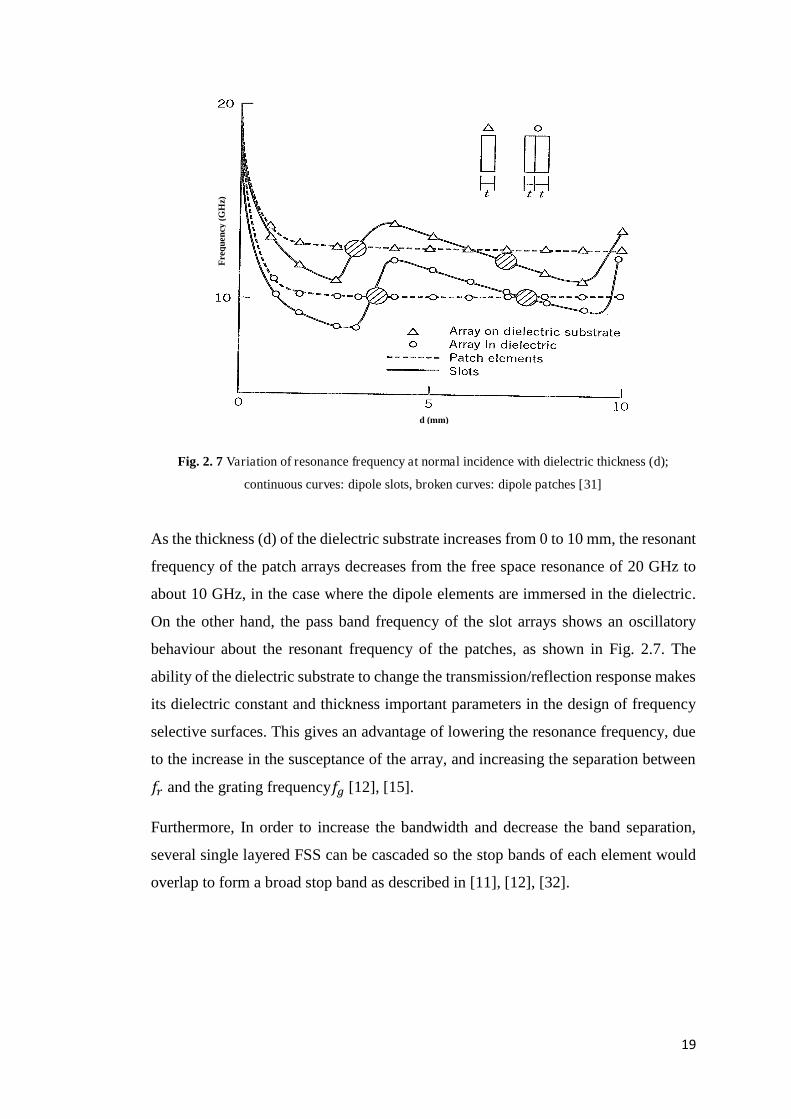
2.3.4 Influence of the supporting dielectric substrate
Frequency selective surfaces are normally supported by a dielectric layer for
mechanical strength, and which affects the transmission or reflection response of the
periodic structures. The addition of the substrate lowers the resonance frequency岫血追岻,
bandwidth, and with appropriate choice can reduce the angular instability. If the
periodic element is sandwiched between two infinitely thick dielectric materials with
relative dielectric constant 香追, the resonance frequency would decrease by a factor
of ヂ香追 , as shown in Fig. 2.6 (a) [11], [31]. Fig. 2.6 (b) shows the effect of substituting
the infinite dielectric with dielectric slabs of a small finite total thickness of に穴 . In
this case, the resonance frequency changes are between 血追 and 捗認ヂ敵認 , and is closer to 捗認ヂ敵認 even when the slab thickness is as small as どどの 膏敵, where 膏敵 is the wavelength
within the dielectric.
However, if the periodic structure is printed on just one substrate, the resonance
frequency would be:
捗認 紐岫敵認袋怠岻【態 (4)
as illustrated in Fig. 2.6 (b). In this case, as the thickness of the substrate decreases,
the resonance frequency increases toward the free space resonance frequency 血追.
Although slot arrays in a conducting sheet do not require additional mechanical
support, dielectric substrates can provide some advantages such as lowering the cut-
off frequency, and increased separation from the grating responses. Fig. 2.7 illustrates
the change of the resonance frequency in the cases of patch and slot arrays when they
are immersed in the dielectric or printed on a dielectric surface of relative
permittivity 香追 噺 ね [31].

18
血追ヂ香追 血追
血追 血追ヂ香追
2 d
血追紐岫香追 髪 な岻【に
1
凧 o
r 托
Frequency
FSS
Infinite dielectric (2d=∞)
FSS
(a) The effect on the resonant frequency when an FSS is immersed in an infinite medium of
relative permittivity 岫而司岻
1
凧 o
r 托
Frequency
FSS
(b) Effect on resonant frequency when the FSS is immersed in finite slabs of thickness d on both sides and on a single sheet
Fig. 2. 6 Effect of dielectric substrate on the resonant frequency fr: (a) infinite thickness and (b) finite
thickness d
d
19
Fig. 2. 7 Variation of resonance frequency at normal incidence with dielectric thickness (d);
continuous curves: dipole slots, broken curves: dipole patches [31]
As the thickness (d) of the dielectric substrate increases from 0 to 10 mm, the resonant
frequency of the patch arrays decreases from the free space resonance of 20 GHz to
about 10 GHz, in the case where the dipole elements are immersed in the dielectric.
On the other hand, the pass band frequency of the slot arrays shows an oscillatory
behaviour about the resonant frequency of the patches, as shown in Fig. 2.7. The
ability of the dielectric substrate to change the transmission/reflection response makes
its dielectric constant and thickness important parameters in the design of frequency
selective surfaces. This gives an advantage of lowering the resonance frequency, due
to the increase in the susceptance of the array, and increasing the separation between 血追 and the grating frequency血直 [12], [15].
Furthermore, In order to increase the bandwidth and decrease the band separation,
several single layered FSS can be cascaded so the stop bands of each element would
overlap to form a broad stop band as described in [11], [12], [32].
d (mm)
Fre
que
ncy
(GH
z)

20
2.2.5 Convoluted elements
Convoluting of element paths has been recommended due to the various benefits on
the performance of frequency selective surfaces. This reduces the resonance
frequency, and increases the band separation with their grating response, while also
reducing the unit cell dimensions. Fig. 2.8 shows examples of convoluting dipole and
cross dipole elements [27], [33], [34].
l
l
l
(a) (b)
Fig. 2. 8 Examples of convoluted elements; (a) convoluted dipoles [27] (b) Convoluted cross dipole
[33]
Arrays of elements such as dipoles have relatively large unit cell size in relation to
their resonance wavelength, and thus, small band separation. Reference [27]
investigates the effect of convoluting simple linear dipoles, and how they show
improved stability toward oblique angles of incidence, with significant reduction in
their resonance frequency.

21
Fig. 2.9 compares the transmission response of linear (un-convoluted) dipole elements
with the convoluted dipoles shown in Fig. 2.8 (a), in the case of normal incidence and
when 肯 噺 ねのソ in TE and TM modes are used. The resonant frequency ranges from
about 13.7 to 14.3 GHz for the simple dipole element to approximately 9 GHz for the
convoluted dipole. The transmission response of the convoluted dipole arrays proved
to be more angular independent, unlike the linear dipoles which do not have a common
-10 dB stop band bandwidth in the case of 0 to 45ゼ oblique incidence.
(a) Linear dipole
(b) Convoluted dipole
Fig. 2. 9 Measured transmission response; (a) linear dipole, (b) convoluted dipole [27]
Frequency (GHz)
S 21 (
dB)
S 21 (
dB)
Frequency (GHz)
TE 45 Normal incidence TM 45

22
This has led to many publications in convoluting elements such as convoluted square
loops [34], convoluted dipoles and cross dipoles [27], [33], interwoven convoluted
dipoles [35], [36], and Hilbert curves [34]. The effectiveness of convolution is judged
by a number of figure of merits and factors such as:
1. Roll off factor, where a value as low as 1.1 can be achieved.
2. 碇牒 Larger values mean smaller cell size for a given resonance wavelength.
3. 挑牒 , where 詣 is the total conductor length.
4. The efficiency of use of the conductor 挑碇 .
Generally, convoluted elements have a number of significant advantages:
1- Low element distortion, on the transmission response, occurring when these
arrays are laid down on curved structures; this is due to their small unit cell
size with respect to surface curvature [12], [33], [34].
2- Improved density of resonant current within the unit cell [33].
3- Convolution facilitating stop band and pass band filters working as low as
400 MHz for cell sizes of about 23 × 23 mm2 [35], [36].
4- Improved insensitivity of response to oblique angles of incidence.
5- Increased separation between resonance and grating frequencies, therefore,
improving the possibility of usable transmission bands above the reflection
bands.
6- Improved figures of merit such as 碇牒 and
挑碇 compared to conventional arrays.
As convoluted elements have shown good stability with regards to oblique angles of
incidence with very small unit cell dimensions, they could play an important role in
the future of controlling the electromagnetic architecture of buildings, where incident
ray angles will be unconstrained [37].

23
2.3 FSS in buildings
The radio spectrum is a finite resource and it is especially increasingly overcrowded
in those frequency bands used for mobile communications from 900 MHz up to
3.6 GHz, and the W-LAN bands from 2.4 GHz to 5.8 GHz. Frequency selective arrays
have been recommended for in building applications [9], [38], in order to improve
spectrum efficiency by the reuse of channels over a short distance, as well as
increasing security and privacy within buildings [39]. In [40], it was concluded that an
improvement of 15 dB in the carrier to interference ratio in indoor wireless
communications can reduce the outage probability by more than a factor of 20. Also
a 10 dB decrease of co-channel interference enables the cell size in square law
propagation conditions to be reduced by about 3.
Fig. 2. 10 Scenarios of FSS applications within a high-rise building (1) Rooms with secured indoor
WLAN and isolated from outside (only allow Emergency TETRA), (2) Solely secured for indoor WLAN
open to outside (TETRA, GSM, DCS, UMTS), (3) Open Rooms with black spots Requiring improved
internal propagation, (4) Enclosed room (allow Emergency Services)
4)
1) 1)
2) 2) 2)
3) 3) 3)
1)
4)

24
Frequency selective surfaces can be employed on walls and windows [9], [41]–[43],
to pass or reflect the communications at the WLAN band in order to reduce the
co-channel interference from adjacent systems or preventing eavesdropping. This
could be by shielding the whole building, or floors, or rooms to modify their
electromagnetic architecture. Fig. 2.10 shows an example of signal propagation
control within buildings.
In addition, the nature of the built environment might require blocking of all radio
propagation except terrestrial trunked radio emergency frequency bands (TETRA),
e.g. floor 4 in Fig. 2.10. This may be the case of theatres, cinemas, prisons and
hospitals. Therefore, a range of designs were investigated including active and
transparent FSS, the latter being fabricated on glass with transparent conducting
materials. Reference [44] suggested FSS panels could be used to control and redirect
signal paths and thus enhance wireless communications especially in shadowed areas
such as corridors.
Numerous convoluted FSS screen have been developed in order to modify the
electromagnetic structure of buildings [36], [37], [45] . Reference [37] demonstrates
convoluted and interwoven FSS arrays designed for mobile communications which
attenuate the mobile and wireless communications bands between 700 MHz and
3 GHz, while passing the general mobile radio systems (GMRS) (462-467 MHz) in
the USA, and the personal mobile radio systems (PMR446) (446 MHz) and the
emergency services TETRA band in Europe.
However, in order to make such use of frequency selective surfaces practical, it is
necessary to manufacture the screens cost efficiently and ideally on environmentally
friendly flexible substrates that can be applied easily to any surface, while also
reducing the material wastage. Reference [46] demonstrated for the first time the
manufacture of dipole FSS arrays using the inkjet printing technology. References
[47], [48] demonstrate also the inkjet printing of simple square loop elements on
textiles and on glass windows. Inkjet printing technology as an additive method of
fabrication has a number of advantages, which attracted research in the field of
antennas, over the subtractive methods such as the chemical copper etching. The
dipole elements in [46] were arranged in a skewed lattice geometry and inkjet printed
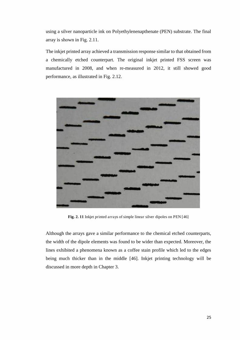
25
using a silver nanoparticle ink on Polyethylenenapthenate (PEN) substrate. The final
array is shown in Fig. 2.11.
The inkjet printed array achieved a transmission response similar to that obtained from
a chemically etched counterpart. The original inkjet printed FSS screen was
manufactured in 2008, and when re-measured in 2012, it still showed good
performance, as illustrated in Fig. 2.12.
Fig. 2. 11 Inkjet printed arrays of simple linear silver dipoles on PEN [46]
Although the arrays gave a similar performance to the chemical etched counterparts,
the width of the dipole elements was found to be wider than expected. Moreover, the
lines exhibited a phenomena known as a coffee stain profile which led to the edges
being much thicker than in the middle [46]. Inkjet printing technology will be
discussed in more depth in Chapter 3.

26
Frequency
Fig. 2. 12 Measured transmission responses of the inkjet printed and chemically etched dipole FSS
arrays
The use of additive technology such as screen or inkjet printing of silver based inks
can result in the elements having low conductivity, and with some variability in the
conductivity [49]. Therefore, the equivalent circuit model shown in Figs. 2.2 (a) and
(b) can be modified to include a resistance element that would affect the transmission
response of the FSS leading to a shallower null depth as resistance increases [49], as
illustrated in Fig. 2.13.
Fig. 2. 13 Equivalent circuit model and the transmission response of square loop elements FSS: in
the case of variable conductivity
-40
-35
-30
-25
-20
-15
-10
-5
0
10 11 12 13 14 15 16 17 18 19 20
S 21(d
B)
Frequency (GHz)
Inkjet printed
Etched
Att
enu
atio
n R
Incr
eas
ing
R
L
C
Low
High

27
2.4 Summary
A review of literature on frequency selective surfaces and its applications has been
presented. The element types that control the filter behaviour of FSS arrays have been
discussed including characteristics such as single or dual polarisation, effect of oblique
angle of incidence, and bandwidth.
The influence of the supporting dielectric substrates on the transmission response of
the FSS and its effect on the bandwidth of operation and sensitivity toward angle of
incidence, have also be described. In addition, the advantages of convoluting elements
were also indicated.
The benefits that could be achieved by using frequency selective surfaces such as the
increase of signal-to-interference ratio and data security within buildings were
reviewed, as well as the fabrication of FSS arrays with the inkjet printing technology.

28
References
[1] R. A. Semplak, “A Quasi-Optical Polarization-Independent Antennas,” IEEE Trans. Antennas Propag., no. 6, pp. 780–785, 1976.
[2] V. Agrawal and W. Imbriale, “Design of a Dichroic Cassegrain Subreflector,” IEEE Trans. Antennas Propag., vol. 27, no. 4, pp. 466–473, 1979.
[3] F. Stefan Johansson, “Analysis and Design of Double-Layer Frequency-Selective Surfaces,” IEE Proc. H Microwaves, Antennas Propag., vol. 132, no. 5, p. 319, 1985.
[4] E. L. Pelton and B. A. Munk, “A streamlined metallic radome,” IEEE Trans. Antennas Propag., no. AP-22, pp. 799–803, 1974.
[5] H. D. Griffi ths and A. M. Vernon, “Planar phase shifting structures for steerable DBS antennas,” in Proc. International Conference on Electromagnetics in Aerospace Applications (ICAP 89), 1989, pp. 45–49.
[6] J. R. James and G. Andrasic, “Superimposed dichroic microstrip antenna arrays,” IEE Proc. H Microwaves Antennas Propag., vol. 135, no. 5, pp. 304–312, 1988.
[7] P. Ingvarson, F. S. Johansson, and L. E. Pettersson, “A dichoric subreflector for a communication satellite,” in Proc. Antennas and Propagation Society International Symposium (AP-S), pp. 1088–1091, 1989.
[8] E. A. Parker, “A linearly-polarized dual-band diplexer in an offset reflector,” Journal of Institution of Electronic and Radio Engineers, vol. 56, no. 3, pp. 111–116, 1986.
[9] M. Philippakis, C. Martel, D. Kemp, R. Allan, S. Massey, M. Clift, S. Appleton, W. Damerell, C. Burton, and E. A. Parker, “Project to demonstrate the ability of Frequency Selective Surface Structures to enhance the spectral efficiency of radio systems when used within buildings,” Ofcom ref AY4464A, pp. 1–58, 2003.
[10] T. K. Wu, Frequency selective surface and grid array. J. Wiley, 1995.
[11] B. A. Munk, Frequency Selective Surfaces: Theory and Design. John Wiley & Sons, 2000.
[12] E. A. Parker, “The Gentleman’s Guide to Frequency Selective Surfaces,” 17th Q.M.W Antenna Symposium, April, pp. 1–18, 1991.
[13] N. Marcuvitz, Waveguide Handbook. IET, 1951.
[14] C. K. Lee and R. J. Langley, “Equivalent-circuit models for frequency-selective surfaces at oblique angles of incidence,” IEE Proc. H Microwaves, Antennas Propag., vol. 132, no. 6, p. 395, 1985.
[15] R. J. Langley and E. A. Parker, “Equivalent circuit model for arrays of square

29
loops,” Electron. Lett., vol. 18, no. 7, p. 294, 1982.
[16] A. E. Yilmaz and M. Kuzuoglu, “Design of the square loop frequency selective surfaces with particle swarm optimization via the equivalent circuit model,” Radioengineering, vol. 18, no. 2, pp. 95–102, 2009.
[17] M. Hosseinipanah, Q. Wu, and C. Zhang, “Design of Square-Loop Frequency Selective Surfaces Utilize C-band Radar Stations,” in International Conference on Microwave and Millimetre Wave Technology (ICMMT),pp. 2–4, 2008.
[18] E. L. Pelton and B. A. Munk, “Scattering from Periodic arrays of crossed dipoles,” IEEE Trans. Antennas Propag., no. 3, pp. 323–330, 1979.
[19] S. M. A. Hamdy and E. A. Parker, “Current distribution on the elements of a square loop frequency selective surface,” vol. 18, no. 14, pp. 1λ81–1983, 1982.
[20] E. A. Parker and S. M. A. Hamdy, “Rings as elements for frequency selective surfaces,” Electron. Lett., vol. 17, no. 17, p. 612, 1981.
[21] E. A. Parker, S. M. A. Hamdy, and R. J. Langley, “Arrays of concentric rings as frequency selective surfaces,” Electron. Lett., vol. 17, no. 23, pp. 0–1, 1981.
[22] Shung-Wu Lee, G. Zarrillo, and Chak-Lam Law, “Simple formulas for transmission through periodic metal grids or plates,” IEEE Trans. Antennas Propag., vol. 30, no. 5, pp. 904–909, 1982.
[23] S. M. A. Hamdy and E. A. Parker, “Influence of lattice geometry on transmission of electromagnetic waves through arrays of crossed dipoles,” IEE Proc. H Microwaves, Opt. Antennas, vol. 129, no. 1, p. 7, 1982.
[24] S. W. Schneider and B. A. Munk, “The scattering properties of Super Dense arrays of dipoles,” Antennas Propagation, IEEE Trans., vol. 42, no. 4, pp. 463–472, 1994.
[25] R. Cahill and E. A. Parker, “Concentric Ring and Jerusalem Cross Arrays as Frequency Selective Surfaces for a 45 ° Incidence Diplexer,” Electron. Lett., vol. 18, no. 8, pp. 313–314, 1982.
[26] E. A. Parker, S. M. A. Hamdy, and R. J. Langley, “Modes of resonance of the Jerusalem cross in frequency-selective surfaces,” vol. 130, no. 3, pp. 203–208, 1983.
[27] E. A. Parker and A. N. A. El Sheikh, “Convoluted dipole array elements,” Electron. Lett., vol. 27, no. 4, p. 322, 1991.
[28] P. S. Taylor, A. C. M. Austin, E. A. Parker, M. J. Neve, J. C. Batchelor, J. T.-P. Yiin, M. Leung, G. B. Rowe, A. G. Williamson, and K. W. Sowerby, “Angular independent frequency selective surfaces for interference control in indoor wireless environments,” Electron. Lett., vol. 48, no. 2, p. 61, 2012.
[29] E. A. Parker and R. J. Langley, “Double-square frequency-selective surfaces and their equivalent circuit,” Electron. Lett., vol. 19, no. 17, pp. 675–677, 1983.

30
[30] S. M. A. Hamdy and E. A. Parker, “Influence of lattice geometry on transmission of electromagnetic waves through arrays of crossed dipoles,” IEE Proc. H Microwaves, Opt. Antennas, vol. 129, no. 1, p. 7, 1982.
[31] P. Callaghan, E. A. Parker, and R. J. Langley, “Influence of supporting dielectric layers on the transmission properties of frequency selective surfaces,” IEE Proc. H Microwaves, Antennas Propag., vol. 138, 1991.
[32] D. A. Palma, W. C. Wong, O. S. Park, and R. Beach, “Broadband frequency selective,” pp. 1–5, 1986.
[33] E. A. Parker, A. N. A. El sheikh, and A. C. de C. Lima, “Convoluted frequency-selective array elements derived from linear and crossed dipoles,” IEE Proc. H Microwaves, Antennas Propag., vol. 140, no. 5, p. 378, 1993.
[34] E. A. Parker and A. N. A. El sheikh, “Convoluted array elements and reduced size unit cells for frequency-selective surfaces,” IEE Proc. H Microwaves, Antennas Propag., vol. 138, no. 1, p. 19, 1991.
[35] E. A. Parker, J. C. Batchelor, R. Chiang, A. G. Williamson, B. Sanz-Izquierdo, M. J. Neve, and K. W. Sowerby, “Frequency selectively screened office incorporating convoluted FSS window,” Electron. Lett., vol. 46, no. 5, p. 317, 2010.
[36] F. Huang, J. C. Batchelor, and E. A. Parker, “Interwoven convoluted element frequency selective surfaces with wide bandwidths,” Electron. Lett., vol. 42, no. 14, p. 788, 2006.
[37] B. Sanz-Izquierdo, E. A. Parker, J.-B. Robertson, and J. C. Batchelor, “Singly and Dual Polarized Convoluted Frequency Selective Structures,” IEEE Trans. Antennas Propag., vol. 58, no. 3, pp. 690–696, Mar. 2010.
[38] A. Newblold, “Designing buildings for the wireless-age,” Computing & Control Engineering Journal, June/July, pp. 18–21, 2004.
[39] E. A. Parker and S. B. Savia, “Fields in an FSS Screened Enclosure,” Proc. IEE, Microwaves, Antennas & Propagation. 16-Aug-2004.
[40] A. H. Wong, M. J. Neve, and K. W. Sowerby, “Performance analysis for indoor wireless systems employing directional antennas in the presence of external interference,” 2005 IEEE Antennas Propag. Soc. Int. Symp., vol. 1A, pp. 799–802, 2005.
[41] N. Qasem and R. Seager, “Frequency selective wall for enhancing wireless signal in indoor environments,” Antennas Propag. Conf. 2009. LAPC 2009. Loughborough., no. November, pp. 573–576, 2009.
[42] G. H. H. Sung, K. W. Sowerby, M. J. Neve, and A. G. Williamson, “A frequency-selective wall for interference reduction in wireless indoor environments,” IEEE Antennas Propag. Mag., vol. 48, no. 5, pp. 29–37, 2006.
[43] N. Qasem and R. Seager, “Studies on enhancing wireless signal for indoor

31
propagation,” in 2010 Loughborough Antennas & Propagation Conference, 2010, pp. 309–312.
[44] D. C. Kemp, C. Martel, M. Philippakis, M. W. Shelley, R. A. Pearson, and I. Llewellyn, “Enhancing radio coverage inside buildings,” IEEE Antennas and Propa. Society International Symposium pp. 783–786, 2005.
[45] E. A. Parker, J.-B. Robertson, B. Sanz-Izquierdo, and J. C. Batchelor, “Minimal Size FSS for Long Wavelength Operation,” Electronics Letters. 13-Mar-2008.
[46] J. C. Batchelor, E. A. Parker, J. A. Miller, V. Sanchez-Romaguera, and S. G. Yeates, “Inkjet printing of frequency selective surfaces,” Electron. Lett., vol. 45, no. 1, p. 7, 2009.
[47] W. G. Whittow, Y. Li, R. Torah, K. Yang, S. Beeby, and J. Tudor, “Printed frequency selective surfaces,” Electron. Lett., vol. 49, no. 13, pp. 1507–1509, 2013.
[48] E. Arnaud, A. Kanso, T. Monediere, and D. Passerieux, “Inkjet Printing of Frequency Selective Surfaces on EBG Antenna Radome,” in The 6th European Conference on Antennas and Propagation (EuCAP 2012), pp. 2693–2696, 2011.
[49] C. Mias, C. Tsakonas, C. Oswald, and B. Street, “An Investigation into the Feasibility of designing Frequency Selective Windows employing periodic structures ( Ref . AY3922 ) Final Report for The Radiocommunications Agency,” 2001.

32
CHAPTER 3: FREQUENCY SELECTIVE
SURFACES PANELS - FABRICATION AND
MEASUREMENTS
3.1 Introduction
This chapter presents an inkjet printing technology overview, including printing
mechanisms, and different sintering methods. The fabrication processes of frequency
selective surface panels using inkjet printing and chemical etching are covered. In
addition, the measurement setup, equipment, and procedures to carry out the
measurements in this study are described. The simulation techniques of the FSS arrays
are also discussed, with different settings to ensure simulation results compared with
measurement.
3.2 Inkjet Printing Technology
3.2.1 Technology Overview
Inkjet printing technology is a subdivision of additive fabrication methods (AM).
Additive manufacturing methods rely on adding different amounts of material layers
upon each other in predetermined positions .Therefore no waste is created, in contrast
to conventional subtractive fabrication methods such as chemical etching which
removes materials in the unwanted regions. AM comprises a number of techniques
according to [1]–[4]:

33
1- Solid based processes or solid sheet systems: such as laminated object
manufacturing (LOM), this technology uses a laser to cut out profiles from
sheet paper supplied from a continuous roll.
2- Powder based process or discrete particle systems: these include technologies
such as selective laser sintering (SLS), which is used to produce sufficient
thermal energy to melt the powder, and three dimensional printing (3-D),
which includes printing a binder or glue layer onto a powder bed to form
a 3-D structure.
3- Liquid based process: such as 2-D inkjet printing.
For several decades subtractive fabrication methods were used in manufacturing
electronic devices. Inkjet printing technology is an emerging alternative fabrication
method that uses metal based conductive inks. Liquid droplets are deposited precisely
onto predefined positions to form conductive tracks on different varieties of substrates.
2-D inkjet printing has been known since the 1960’s as a means of printing by digital
devices such as computers, and was commercialised by companies such as HP and
Canon [4]. Inkjet printing is considered easier, faster and more cost efficient than other
additive technologies, and in addition, its introduction has established the foundation
of several other technologies such as the 3-D printing [5].
In the 1990’s the development of inkjet printing of conductive ink gained interest in
the electronic industry with its promise of producing conductive tracks on low cost,
flexible substrates that were not compatible with subtractive fabrication methods. This
opened the frontiers to various applications such as the manufacture of printed circuit
boards (PCBs), on-body antennas, radio frequency identification (RFID), light
emitting diode (LED), solar cells, sensors for healthcare monitoring, and lately
frequency selective screens [4]–[15].

34
3.2.2 Printing process
The printing process undergoes three main stages in order to produce conductive
tracks:
1- Drop Generation
There are two droplet deposition techniques, (a) continuous inkjet printing (CIJ) and
(b) drop on demand (DOD). In the CIJ printing mechanism, a continuous stream of
liquid drops is ejected under pressure through a small nozzle even when the deposition
is not required. To control the ejection process of each drop, the nozzle is controlled
by a small potential close to the ground [16]. The unwanted drops are deflected by the
electric field to a gutter where the unused ink is recycled, as illustrated in Fig. 3.1(a).
In the contrary, the drop on demand approach allows a control of every drop
individually, leading to more economical deposition than the CIJ mechanism. Droplets
are formed and ejected only with the presence of a pressure pulse in the fluid held in
a chamber behind the printing nozzle, and therefore no waste is formed. The drops are
generated at acoustic frequencies (1 – 20 kHz) in contrast to (20 – 60 kHz) in the case
of the continuous mode. In DOD systems it is possible to control both ejection velocity
and drop size by the control of the pressure pulse used to form the drops [16].

35
(a) Principle operation of continuous inkjet
(b) Principle operation of DOD inkjet
Fig. 3. 1 Principles of operation of (a) Continuous inkjet (CIJ) and (b) drop – on – demand (DOD)
inkjet printers [16]
In the DOD mechanism, there are two methods which are used to generate the pressure
pulse, hence the ejection and drop formation, thermal and piezoelectric printing. In the
thermal DOD printing method or bubble-jet, there is a small thin-film heater located
in the fluid chamber, which in the presence of current it heats the fluid in the ink
trapped in the chamber above its boiling temperature to form a vapour bubble. After
the removal of the passing current, the transfer heat leads to rapid bubble collapse
Thermal Piezoelectric

36
which will be the required pressure pulse, as depicted in Fig. 3.1 (b). In the
piezoelectric method, which is most common, the pressure pulse is formed by direct
mechanical actuation using a piezoelectric transducer which allows the control of drop
size and velocity, as illustrated in Fig. 3.1 (b). Another different feature in the
piezoelectric method is that the fluid tail is long, therefore in order to mitigate any
issues such as drop merging in flight, a standoff distance from the substrate should be
considered, which normally about 2 – 3 mm [16].
2- Drop impact, spreading, and drying
The physical behaviour of the ejected droplets from the print head nozzles reaching
the substrate is described in Fig. 3.2 [17]. According to reference [17], the droplets
experience two spreading mechanisms as they hit the substrate; an initial spontaneous
spreading (by Inertia) for a short time followed by wet spreading (by surface tension)
for a much longer period of time until the droplets reach to the final equilibrium
diameter.
The droplets received by the substrate undergo different mechanisms including solvent
evaporation of the organic solvents (that are normally used as aqueous carrier medium
to ensure the fluidity of the metal ink), cooling through a transition temperature, and
chemical reactions. Therefore, a phase change from a liquid to a solid state occurs
leading to the final required printed shape, which is necessary before going through
the solidification process [15]–[18].
Fig. 3. 2 Inkjet printing process [17]
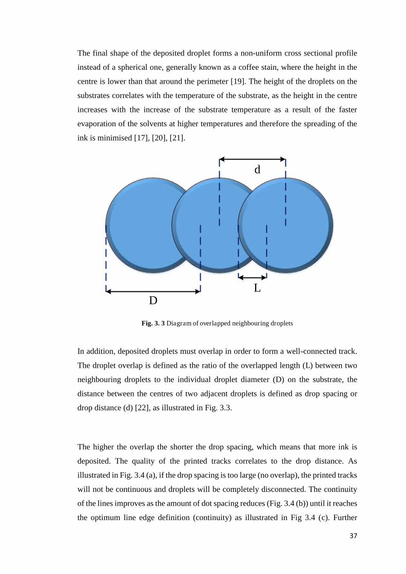
37
The final shape of the deposited droplet forms a non-uniform cross sectional profile
instead of a spherical one, generally known as a coffee stain, where the height in the
centre is lower than that around the perimeter [19]. The height of the droplets on the
substrates correlates with the temperature of the substrate, as the height in the centre
increases with the increase of the substrate temperature as a result of the faster
evaporation of the solvents at higher temperatures and therefore the spreading of the
ink is minimised [17], [20], [21].
d
DL
Fig. 3. 3 Diagram of overlapped neighbouring droplets
In addition, deposited droplets must overlap in order to form a well-connected track.
The droplet overlap is defined as the ratio of the overlapped length (L) between two
neighbouring droplets to the individual droplet diameter (D) on the substrate, the
distance between the centres of two adjacent droplets is defined as drop spacing or
drop distance (d) [22], as illustrated in Fig. 3.3.
The higher the overlap the shorter the drop spacing, which means that more ink is
deposited. The quality of the printed tracks correlates to the drop distance. As
illustrated in Fig. 3.4 (a), if the drop spacing is too large (no overlap), the printed tracks
will not be continuous and droplets will be completely disconnected. The continuity
of the lines improves as the amount of dot spacing reduces (Fig. 3.4 (b)) until it reaches
the optimum line edge definition (continuity) as illustrated in Fig 3.4 (c). Further

38
excessive reduction in the dot spacing might lead to instability in the line definition
leading to the bulging instability as shown in Fig. 3.4 (d).
Fig. 3. 4 Inkjet printed lines with different drop – spacing: (a) no overlap, (b) minimum overlap, (c)
sufficient overlap, and (d) too large overlap (too small drop spacing [16]
3- Sintering of metal nanoparticle inks
In metal nanoparticle inks, a layer of stabilisers commonly from organic materials are
added in order to keep the nanoparticles well-dispersed in the solution [23], [24]. Not
all of these organic solvents are removed during the spreading and drying of the ink
droplets over the substrate. Therefore, the printed lines will have very poor or no
conductivity, and weak mechanical strength and porosity [24], [25]. Thus, a sintering
process is needed to completely remove the organic stabilisers or agents by applying
heat on the printed structures below their melting point. The sintering process involves
3 major steps, joining of the adjacent particles together (neck growth), formation of
interconnecting pore channels (densification), and formation of spherical shape of
particles which tends to flow into the pores within it. As a result, metal particles are
fused together and create one solid piece, and hence, the electrical conductivity and
mechanical strength will be enhanced [26]–[28].

39
There are different methods of sintering used such as the well-known thermal sintering
using conventional ovens. In this case the whole sample will be exposed to heat under
high temperature conditions, typically > 200 °C for > 1hr [23], [24]. However, this
process is not suitable for some thermally sensitive substrates such as polymeric foils
and paper substrates, which would be distorted at temperatures above 120 °C [25],
[29]. Other sintering techniques are more suitable for low treating temperature
substrates and for shorter sintering times, such as intense pulsed light (IPL), laser, and
low pressure argon plasma sintering methods.
In the case of IPL or flash photonic sintering methods, the inkjet printed lines are
exposed to a short pulses of an intense pulsed light with a broad spectrum, ranging
from the ultraviolet (UV) to the infrared (IR), to increase the temperature in the
samples locally and rapidly. The light is only absorbed by the ink, and hence there is
a rapid increase in the temperature within the ink, rather than the substrate which
remains unheated. Photonic sintering time depends on the frequency and the power
level of the exposing light pulse [6], [23], [30], [31].
Another technique is laser sintering, where the silver printed tracks are exposed to a
laser source. The laser scans the printed tracks, which normally requires several passes
to sinter the complete feature. It locally heats the area for a short period of time. In this
case the exposure of the laser beam to the substrate in the areas where there is no ink,
is not harmful [6], [23], [24], [31], [32].
Plasma sintering is considered a low temperature sintering technique most suitable for
thermally sensitive substrates [33]. The metal nanoparticle ink is exposed to plasma,
the inherent active species decompose the organic stabilizers due to chain scission
resulting in the formation of low molar mass compounds, which are evaporated under
the low pressure applied. After removal of the organics, destabilized metal
nanoparticles are able to make direct contact, coalesce and form a percolating
conductive network [6], [33].

40
3.2.3 Defects in the printed structures
The occurrence of defects is a possibility that could arise with any fabrication
technique. The type and the level of defects could affect the quality of the product
especially when manufacturing small electronic devices such as printed circuits where
precision and line continuities are essential. With inkjet deficiencies could mainly
occur at printing and/or during the sintering process. According to reference [34]
defects are divided into two categories:
(i) Macroscopic defects are those which are caused due a partial blockage of
the firing nozzles. A partial blockage causes the fired droplet to break up
into finer ones and/or the droplet may be propelled off the intended course
of jetting (forming ink spray). There is also another type of macroscopic
defect known as satellite drops. These form when the alignment of a jet
breaks up, resulting in a primary drop followed by many finer droplets as
the printing head advances. As a consequence, the droplets on the substrate
are not circular, but pear shaped, as shown in Fig. 3.5. Such imperfections
in the printing process for applications such as printed circuits is
destructive, as a short circuit is likely to occur. Therefore, they should be
avoided by regular cleaning of the nozzle tip [34].
Fig. 3. 5 Satellite drop effect [34]

41
(ii) Microscopic defects are internal voids or flaws during the deposition. The
formation of these voids could take place due to the boiling of the solvent
in the ink due to high temperatures during the drying and the sintering
process, or by the impact of droplets on previously (not fully dried)
deposited layers [34], [35]. Fig. 3.6 shows examples of crack patterns after
drying and thermal sintering (200 °C) for different number of deposited ink
layers (N). The cracks increased with multiple layer deposition [35].
Fig. 3. 6 Microscopic images of crack patterns in silver ink printed lines with width of 0.4mm after
drying and sintering [35]
Such defects would affect the electrical properties of the printed lines leading to a
degradation in the conductivity. Therefore, such issues should be taking into
consideration, for example, by assisting the drying process through applying hot air
on the printed patterns prior to sintering especially in the case of multiple ink layers
[34].

42
3.3 FSS screen fabrication
The FSS screens used in this study were manufactured using inkjet printing technology
at the Organic Materials Innovation Centre (OMIC) at the University of Manchester,
while subtractive chemical etching was done at the University of Kent, in order to
make a comparative performance study.
3.3.1 Inkjet printing of FSS screens
A Dimatix DMP-2800 inkjet printer (Fujifilm Dimatix, Inc., Santa Clara, USA),
shown in Fig. 3.7, was used in the study with a disposable piezo "ink jet" cartridge.
This printer can create and define patterns over an area of about 200 300 mm2 and
handle substrates up to 25 mm thick, with the print head being adjustable in the Z
direction. The nozzle plate consists of a single row of 16 nozzles of 23 m diameter
spaced 254 m apart with typical drop volume of 10 pL, (spot size 40 m). For the
purpose of this study, the cartridge temperature was varied in order to optimize the
jetting conditions. The platen was kept at room temperature [36], unless otherwise
specified. The printer contained a 1.5 mL cartridge (DMC-11610) with the cartridge
temperature adjusted between 30-45 °C.
Two silver nanoparticle inks were used, the first was supplied from Sigma-Aldrich
(SunTronic U5603 from Sun Chemicals). The ink consists of a 20 wt% dispersion of
silver nanoparticles (particle diameter in the range of 150 nm by scanning electron
microscope) in an ethanol/ethylene glycol mixture [37]. The ink was used in
fabricating the FSS samples in Chapters 5 and 6.

43
Fig. 3. 7 Dimatix DMP-2800 inkjet printer
The second ink was the Silverjet silver nanoparticle ink (DGP-40LT-15C), containing
30 – 35% wt silver dispersion in triethylene glycol monomethy ether, supplied also
from Sigma-Aldrich [38]. The Silverjet ink, used for the FSS samples in Chapter 6,
has a particle size less than 50 nm, compared to 150 nm for the SunTronic ink.
Paper is considered one of the best organic-substrates candidates for RF applications
such as RFID tags and FSS. It is not only environmentally friendly, but it is also a very
widely produced material that can undergo large reel-to-reel processing. It is a
candidate in terms of mass production for large FSS panels. This makes paper the
lowest cost material which can give good performance with appropriate coating [8].
The FSS arrays were printed on two representative paper substrates, PEL Nano-P60
paper (PEL paper) having an inorganic micro-porous receiving layer, was obtained
from Printed Electronics Ltd. (Cambridge, UK), and also inkjet tattoo transfer paper
(tattoo paper), having a polymeric receiving layer, which was supplied by Crafty
Computer Paper (Leicester UK) [39]. The transfer papers were chosen due to their
ability of being transferred onto walls, or onto substrates that are problematic to print
on because of their surface properties or overall dimensions. In all cases the substrates
were purged with a flow of air to remove dust particles prior to printing.

44
The reduction of the deposited ink drop spacing increases the conductivity of the
printed lines, as well as the multiple deposition of ink layers. The conductivity of the
silver nanoparticle ink on the transfer paper was investigated in [40], and it was found
that sintering at 135°C for 30 mins gave conductivities of about 5% of bulk silver
using two of deposited ink layers without damaging the substrate.
Reported inkjet work on porous materials such as paper, cardboard, leather and wood
can require many ink layers. Several hours of ink sintering for maximum conductivity
are required. Table. 3.1 summarises some of the inkjet fabricated electromagnetic
structures on different porous substrates. The estimated thickness of 1 layer of
deposited ink is about 1 µm. The number of ink layers reported in Table. 3.1 varies
from 3 – 20 layers, with sintering times as long as 10 hours. This is considered
impractical especially in the case of mass production conditions.
Therefore in this study, the aim was to produce frequency selective surfaces with the
minimum cost possible while achieving acceptable levels of transmitivity or
reflectivity depending on the type of the arrays. Consequently, FSS element trials were
jetted with minimum number of ink layers (1 – 3), and different drop spacing (10 –
20 µm), and shorter thermal sintering times (30 – 60 mins) compared to those in Table
3.1. In the case of printing multiple layers, each layer is allowed to dry for > 120
mins in order to avoid printing defects such as those shown in Fig. 3.6. In addition,
other sintering techniques such as plasma and intense pulsed light (IPL) were also tried
(Chapter 5).

45
TABLE. 3. 1 SUMMARY OF SOME INKJET PRINTED WORK OF ELECTROMAGNETIC STRUCTURES
Reference Substrate Ink
Layers
Sintering
time (hr)
Temp
(C)
Cited (S/m)
[5] Paper 7
12
10
10
120
120
2.5×10⁷
[13] Paper 3 2 120 ~1×10⁷
[41] Paper 5 1 160 1.2×10⁷
[42] Paper 12 Unknown Unknown 0.4 -
2.5×10⁷
[43] Paper Unknown 4 130 ~1×10⁷
[44] Wood
Cardboard
Paper
20
20
15
2
2
1
150
150
150
>2×10⁷
[45] Cardboard 3 1 150 2×10⁷
[46] Paper 12 Unknown Unknown (0.4 -
2.5×10⁷)
[47] Textile
Textile
2 – 4
10
Unknown Unknown (0.3 -
0.5×10⁶)
~1×10⁶
Furthermore, due to the expected variability in the conductivities of the printed
elements, it is necessary to take the required skin depth thickness into consideration
while fabricating the FSS screens. Skin depth effect gives an indication of how deeply
into a conductor electromagnetic field will penetrate at a high frequency. It is defined
as the depth below the surface of a conductor at which the amplitude of an incident
electric field has decreased by a factor 1/e [48]. Variation in element conductivities is
expected owing to several factors such as ink used, number of deposited ink layers,
drop spacing, sintering technique, and element width. Table. 3.2 shows the minimum
required thickness at selected frequencies against conductivities of 1, 10, 20 and 30%
of bulk silver.
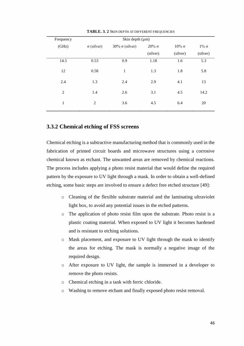
46
TABLE. 3. 2 SKIN DEPTH AT DIFFERENT FREQUENCIES
Frequency
(GHz)
Skin depth (µm)
j (silver) 30% j (silver) 20% j
(silver)
10% j
(silver)
1% j
(silver)
14.5 0.53 0.9 1.18 1.6 5.3
12 0.58 1 1.3 1.8 5.8
2.4 1.3 2.4 2.9 4.1 13
2 1.4 2.6 3.1 4.5 14.2
1 2 3.6 4.5 6.4 20
3.3.2 Chemical etching of FSS screens
Chemical etching is a subtractive manufacturing method that is commonly used in the
fabrication of printed circuit boards and microwave structures using a corrosive
chemical known as etchant. The unwanted areas are removed by chemical reactions.
The process includes applying a photo resist material that would define the required
pattern by the exposure to UV light through a mask. In order to obtain a well-defined
etching, some basic steps are involved to ensure a defect free etched structure [49]:
o Cleaning of the flexible substrate material and the laminating ultraviolet
light box, to avoid any potential issues in the etched patterns.
o The application of photo resist film upon the substrate. Photo resist is a
plastic coating material. When exposed to UV light it becomes hardened
and is resistant to etching solutions.
o Mask placement, and exposure to UV light through the mask to identify
the areas for etching. The mask is normally a negative image of the
required design.
o After exposure to UV light, the sample is immersed in a developer to
remove the photo resists.
o Chemical etching in a tank with ferric chloride.
o Washing to remove etchant and finally exposed photo resist removal.

47
The substrate used in the etching process was a copper clad polyester substrate
(polyethylene terephthalate (PET)), with relative permittivity of 香追 噺 ぬの. The total
thickness of the substrate was 55 µm, in which the copper thickness was about 10 µm.
The photo resists developer used was Potassium Carbonate (K2CO3), and the etching
acid was ferric chloride (FeCl3).
3.4 FSS Measurement set up
Each FSS screen was placed in an aperture in a large absorbing screen of an area of
(2.5 × 2.3 m2), supported with wheels for ease of screen rotation. The size of the
aperture was 210 × 300 mm2, as shown in Fig. 3.8. All FSS screens used in this
research had a physical size of 210 × 300 mm2, except an interwoven convoluted
square slot, and a densely convoluted cross dipole slot design (200 MHz – 1.2 GHz)
which had a physical size of 1 m2, as described in Sections 7.4 and 7.5 (Chapter 7).
Fig. 3. 8 The absorbing screen
Two waveguide horn antennas swept over a frequency range 7 – 20 GHz were
connected to the signal source and the receiver, and placed 1m on either side of the
FSS ( Chapters 4 and 5). For the skewed lattice dipole FSS (L =4.5 mm, P = 5.5 mm)
in Chapter 4, two waveguide horn antennas were also used over the frequency range
(25 – 35 GHz). The FSS screens presented in Chapter 6 were measured using
log – periodic antennas (R&S® HL050, 0.8 – 26.5 GHz [50]) in the frequency range

48
1 – 5 GHz. Fig. 3.9 describes the measurement set up of the FSS arrays used in this
study. The antennas were positioned at height of the centre of the aperture.
Network Analyser
1 m 1 m
Absorbers
FSS screen
Receiving antenna
Transmitting antenna
Fig. 3. 9 FSS transmission response measurement setup
A Marconi Instrument Microwave Test 6200B and vector network analyser (Rohde &
Schwarz, R&S® ZVA50 VNA) operating in the frequency range (10 MHz – 20 GHz),
and (10 MHz – 50 GHz) respectively [51], [52] were used. The transmitted power was
10 dBm. An open free space aperture calibration was taken prior to the mount of the
FSS to take into account any equipment losses e.g. in the antennas and cables. The
calibration was also repeated in the case of different angles of incidence. In the case
of oblique incidence, the absorbing screen was rotated to predefined angles. Each FSS
panel had its transmission response (S21) measured three times, and average values
were used to remove transient channel effects.
In addition, due to the expected variability in the conductivity of the elements in each
FSS panel, a dc point to point resistance measurement was conducted using a digital
multimeter, (Chapters 5 and 6). The measured resistance values where used to
calculate the average resistance, and their standard deviation of the elements in order
to quantify the variation in the conductivity within the FSS panel.

49
Sheet resistance measurements (Chapter 5) were achieved using a 4 point to point
probe method, at the OMIC laboratories. A Jandel multi position wafer probe system
(Jandel Engineering Ltd., Leighton Buzzard, UK) mounted with a cylindrical probe
head made contact with the samples.
Microscopic images of the inkjet printed elements were taken using a Summit 9000
analytical probe station by Cascade Microtech, USA microscope [53] at the University
of Kent laboratories, and scanning electron microscopy (SEM) images were taken
using an EVO® LS 15 system (by Carl Zeiss AG, Oberkochen, Germany) at the OMIC
laboratories.
3.5 FSS Modelling and Simulations
The FSS screens were modelled using Computer Simulation Technology Microwave
Studio® (CST MWS®) [54]. CST uses the finite difference time domain technique
(FDTD). The FDTD is a grid based differential time domain modelling approach. In
FDTD, Maxwell’s equations are formulated as central difference equations,
discretized in space and time. The electric field is solved at a given instance followed
by the magnetic field in the next instant and so on, to update the electromagnetic field
within the defined space [55]–[58]. FDTD techniques has been used in analysing FSS
arrays as was reported in [59]–[62].
CST comprises a number of different solvers, which are each better suited to their
individual applications. For frequency selective surfaces, the frequency solver is
mostly used. Reference [63] gives an example of a modelled infinite bandpass FSS
using the CST frequency solver with unit cell boundaries that virtually repeat the
modelled structure periodically up to infinity, in two directions (x and y). However in
the z direction, open boundaries are used where the Floquet modes are implemented.
Those boundary settings are able to mimic oblique angles of incidence scenarios.
In addition, in order to simulate finite FSS arrays, open boundaries were defined in the
x and y directions with waveguide ports in the z direction of the boundary box. Open
boundary conditions or perfectly matched layers (PML) operate as free space, where
waves interact with the boundaries with minimal reflections. However, modelling a
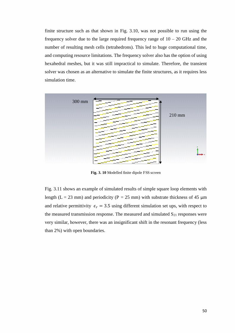
50
finite structure such as that shown in Fig. 3.10, was not possible to run using the
frequency solver due to the large required frequency range of 10 – 20 GHz and the
number of resulting mesh cells (tetrahedrons). This led to huge computational time,
and computing resource limitations. The frequency solver also has the option of using
hexahedral meshes, but it was still impractical to simulate. Therefore, the transient
solver was chosen as an alternative to simulate the finite structures, as it requires less
simulation time.
Fig. 3. 10 Modelled finite dipole FSS screen
Fig. 3.11 shows an example of simulated results of simple square loop elements with
length (L = 23 mm) and periodicity (P = 25 mm) with substrate thickness of 45 µm
and relative permittivity 香追 噺 ぬの using different simulation set ups, with respect to
the measured transmission response. The measured and simulated S21 responses were
very similar, however, there was an insignificant shift in the resonant frequency (less
than 2%) with open boundaries.
300 mm
210 mm

51
Fig. 3. 11 Simulated transmission responses of square loop FSS arrays (L = 23 mm, P = 25 mm,
w=0.2 mm)
In this work, both solvers were considered depending on the nature of the study. The
transient solver was used for the finite arrays in Chapters 4 and 5, while in Chapters 6
and 7 frequency solver unit cell boundaries were used.
Fig. 3. 12 Simulated transmission responses of the square loop FSS arrays with variable
conductivities
-45
-40
-35
-30
-25
-20
-15
-10
-5
0
1 1.5 2 2.5 3 3.5 4 4.5 5
S 21(d
B)
Frequency (GHz)
Measured - finite array
Open boundaries - finite array
Unit cell - infinte array
-45
-40
-35
-30
-25
-20
-15
-10
-5
0
1 1.5 2 2.5 3 3.5 4 4.5 5
S 21(d
B)
Frequency (GHz)
Copper
30% conductivity
10% conductivity
1% conductivity
0.1% conductivity
0.01% conductivity

52
In addition, in order to investigate the influence of conductor conductivity on the FSS
transmission response, the square loop design was simulated (unit cell boundaries)
with different element conductivities of (30, 10, 1, 0.1, and 0.01%) compared to bulk
metal, as described in Fig 3.12. The transmission null depth decreases with the
reduction in the conductivity, which would influence the shielding of the FSS arrays.
Table. 3.3 summarises the simulated results from Fig. 3.12.
TABLE. 3. 3 SIMULATED S21 NULL DEPTHS OF SQUARE LOOP FSS WITH VARIOUS
CONDUCTIVITIES OF FIG. 3.12
Bulk metal conductivity
(%)
S21 (dB) Null reduction %
100 -45 0
30 -40 -11
10 -34 -25
1 -28 -38
0.1 -20 -56
0.01 -13 -71
The element conductivity can be seen to be significant regarding both the depth and
the frequency of the response null and this will be discussed in Chapters 4, 5 and 6.
3.6 Summary
A review of literature on inkjet printing technology using metal nanoparticle inks and
sintering parameters have been presented. The fabrication by inkjet and chemical
etching, of frequency selective surfaces used in this study were outlined. Furthermore,
a description of the equipment used in the fabrication process and measurements has
been covered, as well as the simulation of frequency selective panels in CST.

53
References
[1] “Additive Fabrication (Rapid prototyping, tooling).” [Online]. Availableμ http://www.custompartnet.com/wu/additive-fabrication. [Accessed: 23-Nov-2015].
[2] A. Dolenc, “An Overview Of Rapid Prototyping Technologies In Manufacturing,” Helsinki Univ. of Technoogy, pp. 1–23, 1994.
[3] K. V. Wong and A. Hernandez, “A Review of Additive Manufacturing,” ISRN Mech. Eng., vol. 2012, pp. 1–10, 2012.
[4] I. Gibson, D. Rosen, and B. Stucker, Additive Manufacturing Technologies: 3D Printing, Rapid Prototyping, and Direct Digital Manufacturing. Springer Science, 2010.
[5] V. Lakafosis, A. Rida, R. Vyas, L. Yang, S. Nikolaou, and M. M. Tentzeris, “Progress towards the first wireless sensor networks consisting of inkjet-printed, paper-based RFID-enabled sensor tags,” Proc. IEEE, vol. 98, no. 9, pp. 1601–1609, 2010.
[6] V. Sanchez-Romaguera, S. Wünscher, B. Turki, D. Oyeka, R. Abbel, B. Silvia, T. Daniel J., J. C. Batchelor, E. A. Parker, U. S. Schubert, and S. G. Yeates, “Inkjet printed paper based Frequency Selective Surfaces and on-skin RFID tags; the interrelation between silver nanoparticle ink, paper substrate and low temperature sintering technique selection,” J. Mater. Chem. C, vol. 3, no. 9, pp. 2132–2140, 2015.
[7] V. Sanchez-Romaguera, M. a. Ziai, D. Oyeka, S. Barbosa, J. S. R. Wheeler, J. C. Batchelor, E. a. Parker, and S. G. Yeates, “Towards inkjet-printed low cost passive UHF RFID skin mounted tattoo paper tags based on silver nanoparticle inks,” J. Mater. Chem. C, vol. 1, no. 39, p. 6395, 2013.
[8] M. M. Tentzeris, “Design and Characterization of Novel Paper-based Inkjet-Printed RFID and Microwave Structures for Telecommunication and Sensing Applications,” in 2007 IEEE/MTT-S International Microwave Symposium, 2007, pp. 1633–1636.
[9] J. Ganjei, D. Sawoska, and A. Krol, “Digital Inkjet Printing for Etching Circuits,” J. HKPCA, no. 30, pp. 16–21, 2008.
[10] B. S. Cook, S. Member, and A. Shamim, “Inkjet Printing of Novel Wideband and High Gain Antennas on Low-Cost Paper Substrate,”IEEE Transactions on Antennas and Propagation, vol. 60, no. 9, pp. 4148–4156, 2012.
[11] T. Björninen, J. Virkki, J. Virtanen, L. Sydänheimo, L. Ukkonen, and M. M. Tentzeris, “Inkjet-printing and Performance Evaluation of UHF RFID Tag Antennas on Renewable Materials with Porous Surfaces,”7th European Conference on Antennas and Propagation (EuCAP), pp. 1662–1666, 2013.
[12] J. C. Batchelor, E. A. Parker, J. A. Miller, V. Sanchez-Romaguera, and S. G. Yeates, “Inkjet printing of frequency selective surfaces,” Electron. Lett., vol. 45, no. 1, p. 7, 2009.
[13] G. Shaker, A. Rida, S. Safavi-Naeini, M. M. Tentzeris, and S. Nikolaou, “Inkjet

54
printing of UWB antennas on paper based substrates,” Antennas Wirel. Propag. Lett. IEEE, vol. 10, pp. 111 – 114, 2011.
[14] Q. Wan, G. Yang, Q. Chen, and L.-R. Zheng, “Electrical performance of inkjet printed flexible cable for ECG monitoring,” in 2011 IEEE 20th Conference on Electrical Performance of Electronic Packaging and Systems, 2011, pp. 231–234.
[15] M. Singh, H. M. Haverinen, P. Dhagat, and G. E. Jabbour, “Inkjet Printing-Process and Its Applications,” Adv. Mater., vol. 22, no. 6, pp. 673–685, 2010.
[16] B. Derby, “Inkjet Printing of Functional and Structural Materialsμ Fluid Property Requirements, Feature Stability, and Resolution,” Annu. Rev. Mater. Res., vol. 40, pp. 395–414, 2010.
[17] M. Ikegawa and H. Azuma, “Droplet Behaviors on Substrates in Thin-Film Formation Using Ink-Jet Printing,” JSME Int. J. Ser. B, vol. 47, no. 3, pp. 490–496, 2004.
[18] L. C. Yung, C. C. Fei, J. Mandeep, H. Binti Abdullah, and L. K. Wee, “Synthesis of a nano-silver metal ink for use in thick conductive film fabrication applied on a semiconductor package.,” PLoS One, vol. 9, no. 5, pp. 1–9, 2014.
[19] C.-T. Chen and K.-Z. Tu, “Morphologies of conductive looped liquid lines inkjet-printed on substrate surfaces,” J. Micromechanics Microengineering, vol. 22, no. 5, p. 055001, 2012.
[20] A. M. J. van den Berg, A. W. M. de Laat, P. J. Smith, J. Perelaer, and U. S. Schubert, “Geometric control of inkjet printed features using a gelating polymer,” J. Mater. Chem., vol. 17, no. 7, p. 677, 2007.
[21] D. Soltman and V. Subramanian, “Inkjet-printed line morphologies and temperature control of the coffee ring effect,” Langmuir, vol. 24, no. 5, pp. 2224–2231, 2008.
[22] B. J. Kang and J. H. Oh, “Geometrical characterization of inkjet-printed conductive lines of nanosilver suspensions on a polymer substrate,” Thin Solid Films, vol. 518, no. 10, pp. 2890–2896, 2010.
[23] J. Niittynen, R. Abbel, M. Mäntysalo, J. Perelaer, U. S. Schubert, and D. Lupo, “Alternative sintering methods compared to conventional thermal sintering for inkjet printed silver nanoparticle ink,” Thin Solid Films, vol. 556, pp. 452–459, 2014.
[24] J. Perelaer and U. Schubert, “Inkjet printing and alternative sintering of narrow conductive tracks on flexible substrates for plastic electronic applications,” Radio Freq. Identif. Fundam. Appl. Des. methods Solut., no. February, pp. 265–286, 2010.
[25] K. C. Yung, X. Gu, C. P. Lee, and H. S. Choy, “Ink-jet printing and camera flash sintering of silver tracks on different substrates,” J. Mater. Process. Technol., vol. 210, no. 15, pp. 2268–2272, 2010.
[26] M. V Srikanth, A. S. Songa, S. R. Nali, J. R. Battu, and V. R. M. Kolapalli, “Thermal sintering: A novel technique used in the design, optimization and biopharmaceutical evaluation of propranolol HCl gastric floating tablets,” Drug

55
Dev. Ind. Pharm., vol. 40, no. 1, pp. 33–45, 2014.
[27] B. J. Perelaer, A. W. M. de Laat, C. E. Hendriks, and U. S. Schubert, “Inkjet-printed silver tracks: low temperature curing and thermal stability investigation,” J. Mater. Chem., vol. 18, p. 3209, 2008.
[28] R. E. Njoku and A. R. Kennedy, “Effects of Sintering Temperature on the Density and Porosity of Sodium Chloride Preforms for Open Celled Aluminium Foam Manufacturing,” Nigerian Journal of Technology, vol. 32, no. 1, pp. 117–122, 2013.
[29] J. Perelaer, P. J. Smith, D. Mager, D. Soltman, S. K. Volkman, V. Subramanian, J. G. Korvink, and U. S. Schubert, “Printed electronicsμ the challenges involved in printing devices, interconnects, and contacts based on inorganic materials,” J. Mater. Chem., vol. 20, no. 39, p. 8446, 2010.
[30] J. S. Kang, J. Ryu, H. S. Kim, and H. T. Hahn, “Sintering of Inkjet-Printed Silver Nanoparticles at Room Temperature Using Intense Pulsed Light,” J. Electron. Mater., vol. 40, no. 11, pp. 2268–2277, 2011.
[31] D. Tobjörk, H. Aarnio, P. Pulkkinen, R. Bollström, A. Määttänen, P. Ihalainen, T. Mäkelä, J. Peltonen, M. Toivakka, H. Tenhu, and R. Österbacka, “IR-sintering of ink-jet printed metal-nanoparticles on paper,” Thin Solid Films, vol. 520, no. 7, pp. 2949–2955, 2012.
[32] M.-K. Kim, H. Kang, K. Kang, S.-H. Lee, J. Y. Hwang, Y. Moon, and S.-J. Moon, “Laser Sintering of Inkjet-Printed Silver Nanoparticles on Glass and PET Substrates,” Proc. 10th IEEE Int. Conf. Nanotechnol. Jt. Symp. with Nano Korea, pp. 520–524, 2010.
[33] I. Reinhold, C. E. Hendriks, R. Eckardt, J. M. Kranenburg, J. Perelaer, R. R. Baumann, and U. S. Schubert, “Argon plasma sintering of inkjet printed silver tracks on polymer substrates,” J. Mater. Chem., vol. 19, no. 21, p. 3384, 2009.
[34] J. H. Song and H. M. Nur, “Defects and prevention in ceramic components fabricated by inkjet printing,” J. Mater. Process. Technol., vol. 155–156, pp. 1286–1292, Nov. 2004.
[35] D. J. Lee, J. H. Oh, and H. S. Bae, “Crack formation and substrate effects on electrical resistivity of inkjet-printed Ag lines,” Mater. Lett., vol. 64, no. 9, pp. 1069–1072, 2010.
[36] “PM000040 Rev. 05, DMP-2800 Series - DMP2800GuideVersion2.0.pdf.” [Online]. Available: http://www.lilliu.co.uk/resources/DMP/DMP2800GuideVersion2.0.pdf. [Accessed: 22-Aug-2015].
[37] “Silver nanoparticle ink <150 nm particle size (DLS), 20 wt. % (dispersion in organic solvents) | Sigma-Aldrich.” [Online]. Availableμ http://www.sigmaaldrich.com/catalog/product/aldrich/719048?lang=en®ion=GB. [Accessed: 22-Aug-2015].
[38] “Silver, dispersion nanoparticle, 30-35 wt. % in triethylene glycol monomethyl ether, spec. resistivity 11 たっ-cm, for printing on plastic films | Sigma-Aldrich.” [Online]. Available: http://www.sigmaaldrich.com/catalog/product/aldrich/736465?lang=en®io

56
n=GB. [Accessed: 02-Oct-2015].
[39] “Information Sheet for PEL Nano P60.pdf.” [Online]. Availableμ http://www.printedelectronics.co.uk/Information Sheet for PEL Nano P60.pdf. [Accessed: 22-Aug-2015].
[40] V. Sanchez-Romaguera, M. A. Ziai, D. Oyeka, S. Barbosa, J. S. R. Wheeler, J. C. Batchelor, E. A. Parker, and S. G. Yeates, “Towards inkjet-printed low cost passive UHF RFID skin mounted tattoo paper tags based on silver nanoparticle inks,” J. Mater. Chem. C, vol. 1, no. 39, p. 6395, 2013.
[41] H. F. Abutarboush and A. Shamim, “Conformal and green electronics鳥μ a wideband inkjet printed antenna on paper substrate,” 7th Eur. Conf. Antennas Propag., pp. 3099–3102, 2013.
[42] R. Vyas, V. Lakafosis, H. Lee, G. Shaker, L. Yang, G. Orecchini, A. Traille, M. M. Tentzeris, and L. Roselli, “Inkjet printed, self powered, wireless sensors for environmental, gas, and authentication-based sensing,” IEEE Sens. J., vol. 11, no. 12, pp. 3139–3152, 2011.
[43] S. Kim, M. M. Tentzeris, and S. Nikolaou, “Wearable biomonitoring monopole antennas using inkjet printed electromagnetic band gap structures,” Proc. 6th Eur. Conf. Antennas Propagation, EuCAP 2012, pp. 181–184, 2012.
[44] E. Koski, K. Koski, L. Ukkkonen, L. Sydanheimo, J. Virtanen, T. Bjorninen, and A. Z. Elsherbeni, “Performance of inkjet-printed narrow-line passive UHF RFID tags on different objects,” IEEE Antennas Propag. Soc. AP-S Int. Symp., pp. 537–540, 2011.
[45] H. Saghlatoon, T. Björninen, L. Sydänheimo, M. M. Tentzeris, and L. Ukkonen, “Inkjet-Printed Wideband Planar Monopole Antenna on Cardboard for RF Energy-Harvesting Applications,” IEEE Antennas and Wireless Propagation Letters, vol. 14, pp. 325–328, 2015.
[46] M. M. Tentzeris, S. Kim, R. Vyas, A. Traille, P. Pons, H. Aubert, A. Georgiadis, and A. Collado, “Inkjet-printed ‘Zero-Power’ wireless sensor and power management nodes for IoT and ‘Smart Skin’ applications,” 2014 20th Int. Conf. Microwaves, Radar Wirel. Commun., pp. 1–7, 2014.
[47] W. G. Whittow, Y. Li, R. Torah, K. Yang, S. Beeby, and J. Tudor, “Printed frequency selective surfaces,” Electron. Lett., vol. 49, no. 13, pp. 1507–1509, 2013.
[48] C. A. Balanis, Advanced Engineering Electromagnetics. New York: Wiley, 1989.
[49] T. Laverghetta, Microwave Materials Fabrication Techniques, 2nd ed. Artech House, INc., 1991.
[50] “R&S®HL050 Antenna - Overview - Rohde & Schwarz United States.” [Online]. Available: https://www.rohde-schwarz.com/us/product/hl050-productstartpage_63493-9064.html. [Accessed: 03-Feb-2015].
[51] M. Instruments, “Microwave 6200B Series.”
[52] O. Manual, “Vector Network Analyzers R & S ® ZVA 8 / ZVA 24 / ZVA 40 / ZVA50 R & S ® ZVB 4 / ZVB 8 / ZVB 14 / ZVB 20 R & S ® ZVT 8 / ZVT

57
20.”
[53] “Summit 11K/12K probe station鳥μUser ’ s Guide- Test, Innovating Better, For,” no. 503.
[54] “CST - Computer Simulation Technology.” [Online]. Availableμ https://www.cst.com/. [Accessed: 02-Jun-2015].
[55] T. R. A. Bondeson and P. Ingerlstrom, Computational Electromagnetics. Springer, 2005.
[56] A. Taflove, “Review of the formulation and applications of the finite-difference time-domain method for numerical modeling of electromagnetic wave interactions with arbitraty structures.” Wave Motion, pp. 547–582, 1988.
[57] A. Taflove and K. R. Umiashankar, “The finite-difference time-domain (FD-TD) method for numerical modeling of electromagnetic scattering,” IEEE Trans. Magn., vol. 25, no. 4, pp. 3086–3091, 1989.
[58] K. Yee, “Numerical solution of initial boundry value problems involving Maxwell’s equations in isotropic media,” IEEE Trans. Antennas Propag., vol. 14, no. 3, pp. 302–307, 1966.
[59] W. Yu, S. Dey, and R. Mittra, “Modeling of Periodic Structures using the finite difference time domain (FDTD),” Proc. IEEE AP-S Int. Symp., vol. 1, pp. 594–597, 1999.
[60] Y.-C. A. Kao and R. G. Atkins, “A finite difference-time domain approach for frequency selective surfaces at oblique incidence,” IEEE Antennas Propag. Soc. Int. Symp. 1996 Dig., pp. 1432–1435.
[61] P. Harms, R. Mittra, and W. Ko, “Implementation of the periodic boundary condition in the finite-difference time-domain algorithm for FSS structures,” IEEE Trans. Antennas Propag., vol. 42, no. 9, pp. 1317–1324, 1994.
[62] E. A. Navarro, B. Gimena, and J. L. Cruz, “Modelling of periodic structures using the finite difference time domain method combined with the Floquet theorem,” Electron. Lett., vol. 29, no. 5, p. 446, 1993.
[63] “Polarisation Independent Bandpass FSS.” [Online]. Availableμ https://www.cst.com/Applications/Article/A-Polarisation-Independent-Bandpass-FSS. [Accessed: 04-Dec-2015].

58
CHAPTER 4: STUDY OF THE IMPACT OF
DEFECTS ON THE PERFORMANCE OF FSS
PANELS
4.1 Introduction
The degree to which fabrication errors can be tolerated is an important issue. In the
building industry, low-cost manufacture of acceptable performance components is
required, in contrast to, for example, aerospace systems where the high precision
fabrication of critical components is essential and often involves the use of expensive
specialised materials. The introduction of FSS into the building structure has been
considered as a possible way to improve the signal-to-interference ratio, and data
integrity within buildings by incorporating frequency selective panels into walls,
turning them to smart buildings [1]–[4]. An improvement of 15 dB in the carrier to
interference ratio in indoor wireless communications can reduce the outage probability
by more than a factor of 20. Also a 10 dB decrease of co-channel interference enables
the cell size in square law propagation conditions to be reduced by about 3 [5].
The process of fabricating large chemically etched copper FSS screens is high cost
and requires several process stages if the waste copper is to be reclaimed. Therefore
additive fabrication techniques such as Inkjet technology may be a cost effective
means of production for certain scales of production. Drop-on-demand (DOD) print
technology deposits precise and repeatable drop sizes achieving the resolutions
required for UHF printed circuits on cheap environmentally friendly substrates such
as paper, glass, leather and wood [6]–[12].
However, in printed low- cost mass produced FSS, such as might be required in
application to the built environment for electromagnetic architecture modification,
imperfections might be expected from blockage of printer nozzles, poor surface

59
quality, and non-uniformity in any conducting ink sintering process that might be
adopted [13]–[15]. There are also some physical problems during the process of
installing arrays on walls, e.g. destroying some of the elements due to miss-handling
of the FSS boards or cutting out of some sections for the installation of fixtures and
fittings.
This chapter summarises the results of an investigation of imperfectly fabricated FSS
arrays in which defects were introduced intentionally in two sequential processes. In
the first, array elements were either removed entirely from random locations or small
discontinuities were introduced in the conductors of randomly chosen elements, while
in the second sequence, elements are totally absent in localized clusters that were
introduced at the centres and corners of the panels. Furthermore, the electromagnetic
illumination uniformity and the influence of the oblique incidence and how it affects
the performance of the FSS panels especially the defective arrays, were investigated.
The fabricated designs were arrays of linear dipoles on skewed and square lattices,
square loops, and ring loops [16]–[18]. All structures were fabricated by chemical
etching and were also modelled using CST Microwave Studio® (CST MWS®) to
compare the measurement results with the computer simulation results. In order to
quantify the impact of print error discontinuities, 20 dB null-depth was taken as the
limit of acceptable band stop performance, corresponding to 1% signal transmission
through the structure.

60
4.2 Randomly (Arbitrarily ) missing elements
An issue noticed in the printed FSS arrays was the concern of elements with very high
resistance or being non-conductive. Defects could result from a totally blocked
printing nozzles that could lead to some of the elements totally missing or from partial
nozzles blockage that might cause some discontinuities in the element thus affecting
the performance of the FSS panels. As a consequence, it is of a great importance to
define a tolerable level of maximum defects while the FSS arrays could still provide
an acceptable level of isolation in the intended band of operation.
In this section, elements were deliberately removed, chosen at random locations using
a code that was generated in Matlab™ in a sequence of 10, 20, 30, and 40% of the
total number of the array elements. The arrays were fabricated on a physical area of になど 抜 ぬどど mm2, using chemical etching on a 0.055 mm thick copper clad polyester
substrate with relative permittivity 香追 噺 ぬの and loss tangent 絞 噺 どどに. The
transmission responses of the 4 defective arrays were compared to the perfect FSS
arrays response.
4.2.1 Skewed lattice dipole arrays
The dipole arrays consisted of 374 patch dipoles set on a skewed lattice [16], as shown
in Fig. 4.1. The dipoles were 9.4 mm in length, with horizontal spacing 経捲 噺 な mm,
and vertical spacing 経検 噺 に mm. All dipoles had width 拳 噺 どね mm and
thickness 噺 どどな mm.

61
Fig. 4.1 The linear dipole FSS [19]
Five FSS were made, one was complete (perfect), while in each of the others, 10, 20,
30, and 40% proportions of the elements were absent at random location with no
correlation between the arrays with 10% missing elements and the array with 20%
missing elements for instance, as shown in the modelled version of those arrays in
CST Fig. 4.2.
In the second set, instead of removing the random elements completely, a gap, (g) of どね mm was introduced at the centres of the defective dipoles as shown in Fig. 4.3.
The gaps were introduced in the same location of the missing element shown in
Fig. 4.2 with the same sequence of 10, 20, 30 and 40% to compare the transmittivity
of the FSS arrays in the two scenarios.
To establish whether or not the transmittivity trends for dipoles on skewed lattices also
applies for FSS of different configurations, elements were randomly removed in the
same proportions from other arrays including square loops, dipoles and rings all
arranged on square lattices.

62
(a) Complete (b) 10% missing
(c) 20% missing (d) 30% missing
(e) 40% missing
Fig. 4.2 Modelled dipole arrays with missing elements (a) complete, (b) 10% missing, (c) 20%
missing, (d) 30% missing (e) 40% missing

63
Fig. 4.3 Skewed lattice dipole arrays with discontinuity in some elements [19]
4.2.2 Square lattice dipole arrays
This FSS design was chosen to quantify the effect of missing elements on the FSS
response when the element are arranged in simple square lattice geometry. The
complete FSS contained 475 patch dipole elements with dipole length L and periodicity
P equal to 9.4 and 10.4 mm respectively, as shown in Fig. 4.4.
Fig. 4.4 Square lattice dipole FSS [19]
4.2.3 Square loop arrays
The complete arrays contained 1080 patch square loops arranged in a square lattice
format with length L and periodicity P equal to 6 and 7 mm respectively and element
width w was 0.4 mm, as shown in Fig. 4.5.
L P

64
Fig. 4.5 Square loop FSS [20]
4.2.4 Ring loop arrays
The prefect arrays contained 652 patch Ring loops elements arranged in a square
lattice format with diameter D and periodicity P equal to 7.4 and 9 mm respectively
and ring width (w) was 0.4 mm, as shown in Fig. 4.6.
Fig. 4.6 Ring loops FSS
P
L
P
W
D

65
4.3 Clusters of elements
In addition to the problems addressed in the previous section, also some physical
damage could result during the installation process of FSS panels into walls. Damages
such as cutting of some parts while fitting or damage that could occur in later stages.
Unlike the previous section, elements were removed in clusters of 10% and 20% at
both the centres and the corners of each array type. This investigation was carried on a
total of 5 FSS designs and on a metal sheet screen. Three of the FSS arrays were the
linear dipoles arranged in skewed lattice and square lattice, and square loop arrays
reported in the previous section, and in addition two skewed lattice dipole arrays
designs were fabricated. One was the skewed lattice linear dipole arrays with larger
periodicity than the arrays in Fig. 4.1, where the elements were also arranged with
periodicity P of 15.4 mm, horizontal spacing Dx = 6 mm, and vertical spacing
Dy = 5 mm. Increasing the periodicity led to a decrease in the number of elements within
the same physical area to 174 patch dipoles. The second array was designed to be
resonant around 30 GHz, with element length L of 4.5 mm, P of 5.5 mm, horizontal
spacing Dx = 1 mm, and vertical spacing Dy = 2 mm.
Each of the array types was fabricated 4 times, twice missing 10%; one at the centre
and one at the corner, and twice missing 20% of the total elements at the centre and the
corner. The missing elements clusters were situated either at the centre or at the corner
of the FSS. The 4 fabricated cases of the design from Fig. 4.1 are shown in Fig. 4.7.
The arrays were also modelled in CST Microwave Studio® (CST MWS) for
comparison with measurement.

66
(a)
(b)
(c)
(d)
Fig. 4.7 Fabricated skewed lattice FSS (P = 10.4 mm) with missing dipole clusters of (a) 10% at the centre, (b) 20% at the centre, (c) 10% at the corner and (d) 20% at the corner [21]

67
4.4 Measurements and simulation results
4.4.1 Randomly missing and defective elements
The measured and simulated transmission responses of the skewed lattice dipoles of
Fig. 4.1 are shown in Fig. 4.8. As illustrated, as the number of missing elements
increased, the null depth decreased and a small change in the resonant frequency could
be seen. The scattered absence of 10% of the elements gave a null depth of -22 and
-25 dB in the measured and simulated S21 respectively, compared with the -33 dB of
the perfect complete arrays.
Correspondingly, 20% absence of the elements (75 dipoles) degraded the measured
performance by a further 4 - 5 dB and the 20 dB depth requirement was not met by
3 dB and was exactly -20 dB from simulations. Any further absence in the elements
severely affects the reliability of the FSS panels as the measured null depths were
below 10 dB. Similarly, the introduction of cuts in the centres of 10% of the dipole
arrays from Fig. 4.3, led to only 4 dB reduction in the null depth compared with the
complete arrays as illustrated in Fig. 4.9. Table. 4.1 summarises the measured and
simulated transmission responses of both missing and cut (broken) elements.
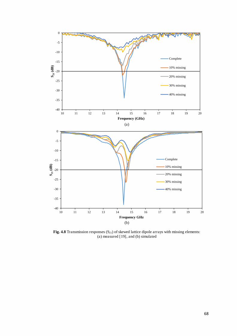
68
(a)
(b)
Fig. 4.8 Transmission responses (S21) of skewed lattice dipole arrays with missing elements:
(a) measured [19], and (b) simulated
-40
-35
-30
-25
-20
-15
-10
-5
0
10 11 12 13 14 15 16 17 18 19 20
S 21(d
B)
Frequency (GHz)
Complete
10% missing
20% missing
30% missing
40% missing
-40
-35
-30
-25
-20
-15
-10
-5
0
10 11 12 13 14 15 16 17 18 19 20
S 21(d
B)
Frequency GHz
Complete
10% missing
20% missing
30% missing
40% missing

69
TABLE. 4.1 COMPARES THE SIMULATED (S) AND MEASURED (M) TRANSMISSION RESPONSES OF SKEWED LATTICE DIPOLE ARRAYS WITH MISSING AND BROKEN
ELEMENTS [19]
% Defective elements
Missing elements Broken elements
S S21 (dB)
M S21 (dB)
S S21 (dB)
M S21 (dB)
0 -38 -33 -38 -33
10 -27 -22 -29 -24
20 -21 -17 -24 -18
30 -15 -10 -16 -10
40 -11 -8 -13 -9

70
(a)
(b)
Fig. 4.9 Transmission responses (S21) of skewed lattice dipole arrays with discontinuities: (a) measured [19] and (b) simulated
The measured and simulated performances of the square lattice dipole arrays
corresponds closely with that of the skewed lattice versions as elements were removed.
Furthermore, the transmission responses of square loops and rings had marginally
deeper (about 2 – 3 dB) nulls than the dipole arrays at the 20% missing element level
and were more clearly deeper at 10%, as summarised in Table. 4.2. The measured and
simulated S21 responses of the arrays are compared with their skewed lattice dipole
equivalents as well in Fig. 4.10.
-40
-35
-30
-25
-20
-15
-10
-5
0
10 11 12 13 14 15 16 17 18 19 20
S 21(d
B)
Frequency (GHz)
Complete
10 % cuts
20 % cuts
30 % cuts
40 % cuts
-40
-35
-30
-25
-20
-15
-10
-5
0
10 11 12 13 14 15 16 17 18 19 20
S 21(d
B)
Frequency (GHz)
Complete 10% cuts
20% cuts 30% cuts
40%cuts

71
TABLE. 4.2 COMPARES THE SIMULATED (S) AND MEASURED (M) TRANSMISSION
RESPONSES OF 3 SQUARE LATTICE FSS ARRAYS WITH THE SKEWED LATTICE DIPOLE ARRAY TRANSMISSION RESPONSE [19], [20]
% Absent
elements
Skewed lattice
dipoles
Square lattice
dipoles
Square loops Ring loops
S
S21
(dB)
M
S21
(dB)
S
S21
(dB)
M
S21
(dB)
S
S21
(dB)
M
S21
(dB)
S
S21
(dB)
M
S21
(dB)
0 -38 -33 -39 -31 -45 -35 -37 -35
10 -27 -22 -23 -23 -31 -29 -27 -26
20 -21 -17 -16 -16 -22 -20 -21 -19
30 -15 -10 -11 -10 -19 -17 -15 -16
40 -11 -8 -8 -9 -17 -15 -13 -14
The results presented in Tables. 4.1 and 4.2 suggest FSS screens can tolerate 15 – 20%
defects in the elements and still provide an interference attenuation of about 20dB.
This would provide adequate shielding from external interference to reduce the outage
probability to the order reported in [5].
Besides, there is also a small shift in the resonant frequency which becomes more
pronounced as the number of missing elements in the arrays increases. The amount of
the frequency shift also differs depending on the FSS type, e.g. in the case of the square
loop arrays, the resonance frequency fr increases by about 2.5% (300 MHz) when 10%

72
of the elements are absent, while 20% absent elements lead to a 4% (450 – 500) MHz
increase.
Fig. 4.10 Measured transmission responses (S21) of different FSS arrays
As then might be deduced, a large increase, of about 1 GHz (8%), occurs when 30 and
40% of the elements are absent, as illustrated in Fig. 4.11. In addition to frequency
drift, the available reflection bandwidth is also affected by element absence. The
measured -10 dB width for the complete square loop FSS is about 4 GHz and this is
reduced by about 2% (50 MHz) and 20% (900 MHz), respectively for 10 and 20%
missing elements, as shown in Fig. 4.12. Larger bandwidth reductions of 30% and
70% are experienced when 30 and 40% of the elements are missing, a situation
expected to be out of specification for any system and in the case of dipole arrays the
null depth does not reach -10 dB as summarised in Fig. 4.12.
-40
-35
-30
-25
-20
-15
-10
-5
0
0 10 20 30 40
S 21(
dB)
Percentage of missing elements %
Skewed lattice dipoles
Square lattice dipoles
Square loops
Ring loops
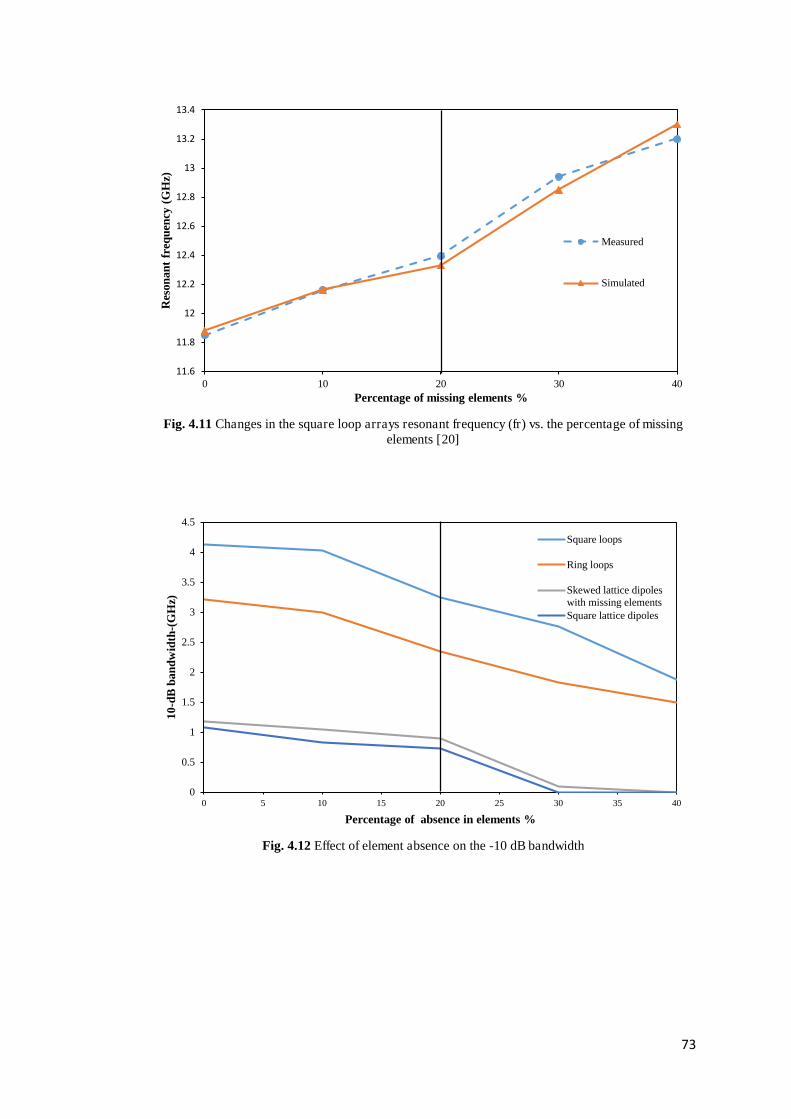
73
Fig. 4.11 Changes in the square loop arrays resonant frequency (fr) vs. the percentage of missing
elements [20]
Fig. 4.12 Effect of element absence on the -10 dB bandwidth
11.6
11.8
12
12.2
12.4
12.6
12.8
13
13.2
13.4
0 10 20 30 40
Res
onan
t fr
eque
ncy
(GH
z)
Percentage of missing elements %
Measured
Simulated
0
0.5
1
1.5
2
2.5
3
3.5
4
4.5
0 5 10 15 20 25 30 35 40
10-d
B b
andw
idth
-(G
Hz)
Percentage of absence in elements %
Square loops
Ring loops
Skewed lattice dipoleswith missing elementsSquare lattice dipoles

74
4.4.2 Clusters of missing elements
The random, non-clustered, absence of 10% and 20% of the elements across the array
as described in the previous section led to a reduction in the transmission null depths
by 11 and 16 dB respectively. The measured transmission responses (S21) for the
clustered design differ depending on the position of the missing element clusters. The
effect of clustering at the array centre is more pronounced, with a 15 and 20 dB
reduction in the transmission null for the design with P = 10.4 mm when 10 and 20%
of the elements were absent, as shown in Fig.4.13.
Fig. 4.13 Measured transmission responses (S21) clustered skewed lattice dipole FSS (P=10.4 mm) [21]
Larger missing element clusters situated in corners were also investigated in the cases
of 30 and 40% where nulls of only -6 and -3 dB respectively were observed meaning
they are unlikely to be of any useful practice. The measured S21 of the skewed lattice
dipole FSS with larger periodicity (P = 15.4 mm) show similar effects to the
(P = 10.4 mm) design in each of the relevant clustering cases. However, in the
P = 15.4 mm design, the random non-clustered absence of 10% and 20% of the
elements reduces the transmission null depths by 9 and 13 dB respectively compared
to the full array. The S21 measurements show lower depth of nulls compared with the
skewed lattice dipole array with smaller periodicity, about 11 dB lower in the case of
the perfect arrays. The effect of clustering at the array centre, however, is close to the
case where the elements were randomly absent and there was 15 and 20 dB reduction
-40
-35
-30
-25
-20
-15
-10
-5
0
10 11 12 13 14 15 16 17 18 19 20
S 21(d
B)
Frequency (GHz)
Perfect array
10% cluster (Centre)
10% cluster (corner)
20%cluster (centre)
20% cluster (corner)

75
in the transmission null when 10 and 20% of the elements were missing, as shown in
Fig. 4.14. This is because the larger periodicity decreases the total number of elements
within the arrays and reduced the coupling between elements compared with the other
designs with smaller periodicities.
Fig. 4. 14 Measured transmission responses (S21) clustered skewed lattice dipole FSS with larger periodicity (P=15.4 mm) [21]
The random absence of 10% and 20% of the elements across the square lattice dipole
array, from Fig. 4.4, led to reductions in the transmission null depths by about 8 and
15 dB respectively. The effect of clustering at the array centre is more pronounced,
with a 13 and 21 dB reduction in the transmission null depths when 10 and 20% of the
elements were missing, as shown in Fig. 4.15.
The clustering effect also causes a shift of about 5 – 10% in the resonance frequency,
(fr). The impact of clustering at the corners of the arrays is less apparent than clustering
at the centre as illustrated in Table. 4.3.
-25
-20
-15
-10
-5
0
10 11 12 13 14 15 16 17 18 19 20
S 21(d
B)
Frequency (GHz)
Perfect array
10%(Distributed)
10% cluster(Centre)
10% cluster(corner)
20%cluster(centre)
20% cluster(corner)

76
Fig. 4.15 Measured transmission responses (S21) clustered square lattice dipole FSS [21]
TABLE. 4.3 COMPARES THE MEASURED TRANSMISSION RESPONSES OF THE 3 DIFFERENT FSS ARRAY TYPES IN THE CASE OF RANDOMLY DISTRIBUTED (MISSING) ELEMENTS AND
CLUSTERS OF MISSING ELEMENTS [21]
-40
-35
-30
-25
-20
-15
-10
-5
0
10 11 12 13 14 15 16 17 18 19 20
S 21(d
B)
Frequency (GHz)
Perfect array
10% Cluster(Centre)10% Cluster(Corner)20% Cluster(Centre)20% Cluster(Corner)
% Absent elements
Skewed lattice
P=10.4 mm
M
S21 (dB)
Skewed lattice
P=15.4 mm
M
S21 (dB)
Square lattice
P=10.4 mm
M
S21 (dB)
0% -33 -23 -31
10% (distributed)
-22 -14 -23
10% at centre
-18 -13 -19
10% at corner -22 -18 -25
20% (distributed)
-17 -9 -16
20% at centre -14 -9 -13
20% at corner
-17 -14 -17

77
A similar clustering test was carried on square loop elements arrays and the skewed
lattice dipole arrays (L =4.5 mm, P = 5.5 mm) resonating at about 30 GHz. The effect
of clustering on these arrays was similar to the dipole arrays (P = 10.4 and 15.4 mm),
where the effect is most severe at the centre of the arrays, as illustrated in Figs. 4.16
and 4.17.
Fig. 4.16 Measured transmission responses (S21) square loop FSS arrays
Fig. 4.17 Measured transmission responses of the clustered skewed lattice dipole arrays (30GHz)
-45
-40
-35
-30
-25
-20
-15
-10
-5
0
7 8 9 10 11 12 13 14 15 16 17 18
S 21(d
B)
Frequency (GHz)
0%
10%
10% Centre
10% Corner
20%
20% Centre
20% Corner
-40
-35
-30
-25
-20
-15
-10
-5
0
25 26 27 28 29 30 31 32 33 34 35
S 21(d
B)
Frequency (GHz)
Complete
10% cluster(centre)
20% cluster(corner)
20% cluster(centre)
10% cluster(corner)

78
The effect of introducing randomly located absent and broken elements discussed in
the previous section, concluded that errors of less than 20% of the elements could be
accepted while still achieving a depth of null of -20 dB. However, it now appears that
clusters of 10% missing elements at the centre on the array cause the null depth to be
less than 20 dB.
However, the deleterious effect of clustering is lower than might be expected,
especially for 20% at the corners of the arrays. This arises because of illumination taper
of the beams of the transmit and receive antennas used in both the measurements and
simulations. Simulations agreed with the measured results in the case of randomly
distributed non-clustered missing elements and also for the case of 10% clusters at the
centre of the arrays. When the clusters were situated at the corners, the agreement with
measurement was poor. The 20% cluster simulations did not match the measurements
well for any position, and this is thought to be due, at least in part, to the simulated
illumination profile which differed from the practical case.
4.4.3 Clustering a metal sheet
In a way of trying to understand the uniformity of the illumination profile, a metal
sheet with the same physical size as the FSS screens was chosen and holes were cut
equal in size to element clusters of 10 and 20% of the arrays previously discussed.
The holes were located in the centres and corners of the sheet identically to the missing
FSS cluster positions.
The introduction of those gaps (slots) is expected to alter the S21 response and instead
of total reflection in the case of perfect metal sheet, there would be some signal
transmission to go through. The aim was to compare the measured transmission
responses (S21) of the perfect metal sheet with the 10 and 20% introduced gaps at the
centres and corners of the metal sheets. As expected the metal sheet provided high
reflection within the frequency swept band and the measurements gave a rejection
level of about -35 dB. The transmission responses for the 10 and 20% clusters at the
centres, however, do not agree with their counterparts where the clusters were
introduced at the corners. For example, the 10 and 20% clusters at the centres had
transmission responses of less than -10 dB in the frequency band of interest, however,

79
their counterparts which were localized at the corner were about -20 dB suggesting
that there was less than 1% of the signal going through, as illustrated in Fig.4.18. This
was deemed to be a consequence of illumination beam tapering in the measurement
and will be investigated in Section 4.5.
Fig. 4.18 Measured transmission responses (S21) of clusterd metal sheets
-40
-35
-30
-25
-20
-15
-10
-5
0
6.5 7.5 8.5 9.5 10.5 11.5 12.5 13.5 14.5 15.5 16.5 17.5 18.5
S 21(d
B)
Frequency (GHz) Metal sheet Metal sheet 10% gap Centre Metal sheet 10% gap Corner
Metal sheet 20% gap Centre Metal sheet 20% gap Corner
80
4.5 Illumination
Changes in the illumination profile across an FSS integrated into a wall could be
significant in a real building environment due to multipath and varied incidence angles,
meaning the position of missing element clusters may change in importance with time.
In this section, different approaches were adopted to investigate the influence of the
illumination profile across the FSS arrays; one by removing randomly 20% of the
dipole elements described in Fig. 4.1 in four random locations. The locations were
randomly chosen (not clustered) through running a code in Matlab™ four times, then
the four FSS arrays were fabricated and measured. The other approach was by focusing
the beam of the transmitting antenna at different locations of the FSS arrays. Finally,
the effect of oblique angle of incidence (事 = 0° to 60°) on the transmission responses
of the square loop arrays when elements are absent in random locations is also
investigated.
4.5.1 Removing 20% of elements at random locations
75 dipole elements were removed in four totally different scattered locations from the
skewed lattice dipole arrays in Fig. 4.1. The transmission nulls of the arrays varied
between 14 to 20 dB, as shown in Fig. 4.19. These results support the observation that
the illumination profile is not totally uniform as found from the clustering study,
however, the impact is less prominent as the missing elements were not focused
(clustered) at the centres of the arrays.
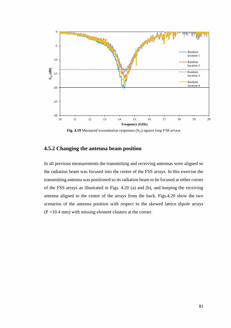
81
Fig. 4.19 Measured transmission responses (S21) square loop FSS arrays
4.5.2 Changing the antenna beam position
In all previous measurements the transmitting and receiving antennas were aligned so
the radiation beam was focused into the centre of the FSS arrays. In this exercise the
transmitting antenna was positioned so its radiation beam to be focused at either corner
of the FSS arrays as illustrated in Figs. 4.20 (a) and (b), and keeping the receiving
antenna aligned to the centre of the arrays from the back. Figs.4.20 show the two
scenarios of the antenna position with respect to the skewed lattice dipole arrays
(P =10.4 mm) with missing element clusters at the corner.
-30
-25
-20
-15
-10
-5
0
10 11 12 13 14 15 16 17 18 19 20
S 21(d
B)
Frequency (GHz)
Randomlocation 1
Randomlocation 2
Randomlocation 3
Randomlocation 4

82
(a)
(b)
Fig. 4.20 Transmitter antenna alignment at the (a) un-clustered corner (b) clustered corner
The measured transmission responses of the arrays in both scenarios fluctuated
depending on the position of the transmitting antenna. Figs. 4.21 (a) and (b) describe
the differences in the performance of the arrays in both scenarios.

83
(a)
(b)
Fig. 4.21 Measured transmission responses of the skewed lattice dipole arrays (P=10.4 mm) when the transmitter antenna aligned to (a) un-clustered corner (b) clustered corner of the arrays
-35
-30
-25
-20
-15
-10
-5
0
10 11 12 13 14 15 16 17 18 19 20
S 21(d
B)
Frequency (GHz)
Complete
10% Cluster (Centre)
10% Cluster (Corner)
20% Cluster (Centre)
20% Cluster (Corner)
-35
-30
-25
-20
-15
-10
-5
0
10 11 12 13 14 15 16 17 18 19 20
S 21(d
B)
Frequency (GHz)
Complete
10% Cluster (Centre)
10% Cluster (Corner)
20% Cluster (Centre)
20% cluster (Corner)

84
The transmission response of the complete (perfect) array was not affected by the
position of the antenna apart from a very small shift of less than 1% in the resonance
frequency. The influence was more pronounced in the case of the arrays with cluster
of missing elements either at the centres or the corners. In the case where the
transmitting antenna was aligned at the top-left corner of the arrays, the arrays with 10
and 20% clusters at the corner had null depths deeper than the 20 dB benchmark,
however, the arrays with clusters at the centre were much below -20 dB. In contrast,
when the transmitter was aligned to the top-left corner (centre of the corner gap) the
transmission responses of the arrays with clusters of missing elements were the
opposite where the corner clusters had much lower null depths than the clusters at the
centres, as summarised in Table. 4.4. This experiment was applied on the dipole
elements arranged in square lattice geometry and the skewed lattice dipole arrays with
the larger periodicity (P = 15.4 mm) and both gave similar results. This shows the
transmission responses (null depths) of the FSS panels could be affected by the non-
uniformity in the illumination profile as described in Table.4.4.
TABLE. 4.4 SUMMARISES THE MEASURED TRANSMISSION RESPONSES (S21) IN dB OF THE DIPOLE FSS ARRAYS
% Absent elements
Top corner
M
S21 (dB)
Gap
M
S21 (dB)
0% -33 -33
10% at centre -18 -28
10% at corner -27 -13
20% at centre -12 -19
20% at corner
-22 -8

85
4.5.3 Oblique angle of incidence
The sensitivity of any FSS arrays toward the oblique angle of incident varies depending
on the elements. It is well-known that dipole elements are more sensitive to oblique
wave incidence when compared with the dual polarised elements such as crossed
dipoles, square and ring loop arrays and convoluted elements which have greater
stability toward oblique angle of incidence [22]–[25]. However, with the presence of
errors in the arrays, the impact of oblique angle of incidence could be significant for
the null depths.
For that reason, the square loop arrays with 10 and 20% of the elements randomly
absent were chosen and their transmission responses were measured with angles of
incidence (事) varied between 0° – 60° and compared with the transmission responses
of the perfect square loop FSS, as described in Fig. 4.22. As mentioned earlier, the
absence (not clustered) of up to 20% of elements in square loop arrays when they are
distributed randomly was tolerable while still achieving the benchmark isolation level
of about 20 dB.
The null depths of the perfect arrays seem to be much more resilient in comparison
with the defective arrays. The null depths of the perfect arrays seem to be much more
resilient in comparison with the defective arrays, while their null depths are more
affected especially in the case of the arrays with 20% missing elements as the angle of
incidence increases. In a building environment, normal signal incidence could be a
very difficult scenario due to reflections and, multipath that the signal would endure,
however, it seems that the FSS arrays with errors of about 10 – 15%, randomly
distributed and clusters, could actually provide good reflectivity of more than 20 dB.

86
(a)
(b)
(c)
Fig. 4. 22 Influence of oblique angle of incidence on the measured transmission responses of square loop arrays (a) perfect arrays (b) arrays with 10% missing elements (c) arrays with 20% missing
elements
-35
-30
-25
-20
-15
-10
-5
0
8 9 10 11 12 13 14 15 16 17 18
S 21(d
B)
Frequency (GHz)
0% - 0
0%-30
0%-45
0%-60
-35
-30
-25
-20
-15
-10
-5
0
8 9 10 11 12 13 14 15 16 17 18
S 21dB
Frequency (GHz)
10% - 0
10% -30
10%- 45
10%- 60
-25
-20
-15
-10
-5
0
8 9 10 11 12 13 14 15 16 17 18
S 21(d
B)
Frequency (GHz)
20%- 0 20%- 30
20% -45 20% -60

87
4.6 Conclusion
As an indication of the improvement in wireless coverage that might be obtained
through the use of FSS in buildings, suppressing the external interference by 15 dB
can reduce the outage probability in mobile communications by more than a factor of
20 [5]. Furthermore, in square law propagation conditions a 10 dB attenuation of the
co-channel interference level shortens the co-channel separation required, and
therefore the cell size, by a factor of about three. The results presented here
demonstrate that meeting such performance requirements should be readily achievable
using manufacturing methods that do not meet the quality standards demanded for
applications such as, for example, might be found in multiband satellite
communication systems.
The effect of introducing randomly located absent and broken elements allows us to
conclude that about 15 – 20% defects in the arrays could be accepted while still
achieving a depth null of -20 dB [19], [20]. This would provide adequate shielding from
external interference to reduce the outage probability to the order reported in [4], [5].
The amount of defects in the arrays depends of the type of the FSS panels and
periodicity as square loop arrays null depths for example indicated greater resistance
toward defects compared with a dipole element array arranged in square and skewed
lattice geometries. However, in the absence of strong clustering, which in the extreme
case would imply an aperture in the array, it appears that clusters of 10% missing
elements at the centre on the array cause the null depth to be less than 20 dB [21].
Nevertheless, the deleterious effect of clustering is lower than might be expected,
especially for 20% at the corners of the arrays, this is a consequence of illumination
tapering in the measurements. Simulations agreed with the measured results in the case
of randomly distributed non-clustered missing elements and also for the case of 10%
clusters at the centre of the arrays. When the clusters were situated at the corners, the
agreement with measurement was poor.

88
The 20% cluster simulations did not match the measurements well for any position,
and this is thought to be due, at least in part, to the simulated illumination profile which
differed from the practical case. Larger missing element clusters situated in corners
were also investigated for the skewed lattice with P =10.4 mm and in the cases of 30
and 40% it was found that the nulls of only -6 and -3 dB respectively meaning they are
unlikely to be of use. In the extreme illumination profile dis-uniformity across an FSS
wall, only 10% distributed error could be tolerated, as the arrays with clusters of
missing elements resulted in unpredictable null depths depending on the position of the
transmitting antenna.

89
References
[1] E. A. Parker, J.-B. Robertson, B. Sanz-Izquierdo, and J. C. Batchelor, “Minimal size FSS for long wavelength operation,” Electron. Lett., vol. 44, no. 6, p. 394, 2008.
[2] M. Philippakis, C. Martel, D. Kemp, S. Appleton, R. Pearson, and E. A. Parker, “Application of FSS Structures to Selectively Control the Propagation of signals into and out of buildings, Annex 3,” Ofcom ref AY4464, pp. 1–54, 2004.
[3] E. A. Parker, J. C. Batchelor, R. Chiang, A. G. Williamson, B. Sanz-Izquierdo, M. J. Neve, and K. W. Sowerby, “Frequency selectively screened office incorporating convoluted FSS window,” Electron. Lett., vol. 46, no. 5, p. 317, 2010.
[4] G. Sung, K. Sowerby, M. Neve, and A. Williamson, “A Frequency-Selective Wall for Interference Reduction in Wireless Indoor Environments,” IEEE Antennas Propag. Mag., vol. 48, no. 5, pp. 29–37, Oct. 2006.
[5] A. H. Wong, M. J. Neve, and K. W. Sowerby, “Performance analysis for indoor wireless systems employing directional antennas in the presence of external interference,” 2005 IEEE Antennas Propag. Soc. Int. Symp., vol. 1A, pp. 799–802, 2005.
[6] B. S. Cook, S. Member, and A. Shamim, “Inkjet Printing of Novel Wideband and High Gain Antennas on Low-Cost Paper Substrate,” IEEE Transactions on Antennas and Propagation, vol. 60, no. 9, pp. 4148–4156, 2012.
[7] J. Ganjei, D. Sawoska, and A. Krol, “Digital Inkjet Printing for Etching Circuits,” J. HKPCA, no. 30, pp. 16–21, 2008.
[8] J. C. Batchelor, E. A. Parker, J. A. Miller, V. Sanchez-Romaguera, and S. G. Yeates, “Inkjet printing of frequency selective surfaces,” Electron. Lett., vol. 45, no. 1, p. 7, 2009.
[9] M. M. Tentzeris, “Design and Characterization of Novel Paper-based Inkjet-Printed RFID and Microwave Structures for Telecommunication and Sensing Applications,” in 2007 IEEE/MTT-S International Microwave Symposium, 2007, pp. 1633–1636.
[10] G. Shaker, A. Rida, S. Safavi-Naeini, M. M. Tentzeris, and S. Nikolaou, “Inkjet printing of UWB antennas on paper based substrates,” Antennas Wirel. Propag. Lett. IEEE, vol. 10, pp. 111 – 114, 2011.
[11] Q. Wan, G. Yang, Q. Chen, and L.-R. Zheng, “Electrical performance of inkjet printed flexible cable for ECG monitoring,” in 2011 IEEE 20th Conference on Electrical Performance of Electronic Packaging and Systems, 2011, pp. 231–234.
[12] R. D. Seager, J. Bowman, R. Philpott, a. Chauraya, M. Broughton, and N. Nimkulrat, “Fabric based frequency selective surfaces using weaving and screen printing,” Electron. Lett., vol. 49, no. 13, pp. 1507–1509, 2013.
[13] J. H. Song and H. M. Nur, “Defects and prevention in ceramic components fabricated by inkjet printing,” J. Mater. Process. Technol., vol. 155–156, pp. 1286–1292, Nov. 2004.

90
[14] B. J. Perelaer, A. W. M. de Laat, C. E. Hendriks, and U. S. Schubert, “Inkjet-printed silver tracks: low temperature curing and thermal stability investigation,” J. Mater. Chem., vol. 18, p. 3209, 2008.
[15] D. Soltman and V. Subramanian, “Inkjet-printed line morphologies and temperature control of the coffee ring effect,” Langmuir, vol. 24, no. 5, pp. 2224–2231, 2008.
[16] S. M. A. Hamdy and E. A. Parker, “Influence of lattice geometry on transmission of electromagnetic waves through arrays of crossed dipoles,” IEE Proc. H Microwaves, Opt. Antennas, vol. 129, no. 1, p. 7, 1982.
[17] R. J. Langley and E. A. Parker, “Equivalent circuit model for arrays of square loops,” Electron. Lett., vol. 18, no. 7, p. 294, 1982.
[18] E. A. Parker and S. M. A. Hamdy, “Rings as elements for frequency selective surfaces,” Electron. Lett., vol. 17, no. 17, p. 612, 1981.
[19] B. M. Turki, E. A. Parker, J. C. Batchelor, M. A. Ziai, S. G. Yeates, and V. Sanchez-Romaguera, “Influence of defective elements on performance of frequency selective surfaces,” Electron. Lett., vol. 49, no. 17, pp. 1054–1055, Aug. 2013.
[20] B. M. Turki, E. A. Parker, M. A. Ziai, J. C. Batchelor, V. Sanchez-Romaguera, and S. G. Yeates, “Study of printing errors in digitally fabricated FSS,” in 2013 Loughborough Antennas & Propagation Conference (LAPC), 2013, pp. 429–432.
[21] B. M. Turki, E. A. Parker, M. A. Ziai, J. C. Batchelor, V. Sanchez-Romaguera, and S. G. Yeates, “Study of clusters of defects in low-cost digitally fabricated frequency selective surfaces,” in The 8th European Conference on Antennas and Propagation (EuCAP 2014), 2014, pp. 779–801.
[22] R. Cahill and E. A. Parker, “Concentric Ring and Jerusalem Cross Arrays as Frequency Selective Surfaces for a 45 ° Incidence Diplexer Hydrogen-induced DLTS Signal in Pd / n-Si Schottky Diodes,” vol. 18, no. 8, pp. 313–314, 1982.
[23] C. K. Lee and R. J. Langley, “Equivalent-circuit models for frequency-selective surfaces at oblique angles of incidence,” IEE Proc. H Microwaves, Antennas Propag., vol. 132, no. 6, p. 395, 1985.
[24] T. K. Wu, Frequency selective surface and grid array. J. Wiley, 1995.
[25] B. A. Munk, Frequency Selective Surfaces: Theory and Design. John Wiley & Sons, 2000.
91
CHAPTER 5: INKJET PRINTING OF SOLID AND
FRAME DIPOLE ELEMENT FREQUENCY
SELECTIVE PANELS
5.1 Introduction
The wide spread of wireless technologies in recent years, together with the era of
Internet of Things, particularly in the built environment, has increased concerns for
information security, as well as for the quality of communication arising from adjacent
sources of interference, as many of the wireless technology bands have become
congested. Various means of improving indoor communication have been considered,
such as frequency reuse by reducing the size of the wireless cells. A relatively new
approach is to modify the electromagnetic structure of buildings, turning them into
smart buildings. Frequency selective panels have been proposed in order to improve
the signal to interference ratio and also to mitigate the issue of user privacy [1]–[3].
Inkjet printing of FSS on a range of different substrates such as paper based, textile,
glass and polyethylene naphthalate (PEN), with electromagnetic performances similar
to those of the chemically etched equivalents have recently been reported [4]–[6].
Since the technology is an additive, mask free printing method, where conducting
tracks of metal nanoparticle based inks can be deposited on demand, it is a potentially
lower-cost fabrication technique than subtractive wet etching methods, with
potentially lower material wastage, whilst being compatible with a wide range of
cheap and environmentally friendly materials including paper, glass and leather
[7]–[10]. Inkjet printing technology has also a potential advantage over chemical
etching as newer technologies are capable of producing very fine pico-litre and femto-
litre sized droplets, enabling the deposition of sub 0.1 mm lines which in turn can
reduce the size of electronic circuits.

92
Minimization of the amount of ink used is desirable in reducing both cost and
environmental impact; however there remains a major challenge in overcoming the
greater risk of defects in the printed elements which in turn would affect the
performance of the FSS [11], [12]. Such defects are typically elements with high
electrical resistance which are equivalent to absent elements, or with total
discontinuities in the conducting path as was described in Chapter 4 and in [13], [14].
The level of -20 dB isolation (null depth) has also been chosen in this chapter as a
benchmark level [14].
The aims of this chapter are to manufacture frequency selective panels at low-cost,
using the minimum amount of deposited ink on paper based substrates, whilst offering
acceptable transmission performance. Trials of FSS panels were made with the
purpose of optimising the manufacturing process in order to achieve the best
performance with the least amount of deposited ink and sintering time. The trials
involved examining two paper substrates engineered for inkjet printing, different
sintering techniques such as thermal, plasma, and photonic with different sintering
time periods. Furthermore, the elements were also printed with different drop-spacing,
and number of deposited ink layers.
Trials were also made of elements in which conductors were deposited only at the
dipole edges (frame elements), where the induced surface currents were likely to be
maximum, thereby making savings in ink, and yet still achieving the benchmark
isolation level of reflection of -20 dB [13], [14]. Furthermore, the deposition of an
extra ink layer in the form of a frame dipole superimposed upon a solid dipole was
also investigated, and compared in terms of ink savings and isolation level with a solid
dipole fabricated with the two layers of deposited ink. An element resistance study of
all FSS designs is also reported here in order to quantify the relation between the level
of isolation and the dc resistance.

93
5.2 FSS design and manufacturing parameters
The FSS design of linear dipole elements arranged in a skewed lattice geometry,
presented in Section 4.2.1 [14], [15] was chosen in order to evaluate the performance
of the inkjet printed panels with their chemically etched counterparts that were etched
on a copper clad polyester substrate of thickness 0.045 mm with relative permittivity
of 鉛嘆 簡 ぬの and loss tangent げ 噺 どどに and metal thickness of 0.01mm .
A Dimatix DMP-2800 inkjet printer was used in this study using a disposable piezo
"ink jet" cartridge. For the purpose of this study, the cartridge temperature was varied
in order to optimize the jetting conditions. The platen was kept at room temperature
[16]. The printer contained a 10 pl cartridge (DMC-11610) with the cartridge
temperature adjusted between 30 – 45 °C.
The elements were printed using the SunTronic silver nanoparticle ink which was
supplied from Sigma-Aldrich (SunTronic U5603 from Sun Chemicals) [17]. The
arrays were printed on two paper class substrates, PEL Nano-P60 paper (PEL paper)
having an inorganic micro-porous receiving layer, and also transfer paper
(tattoo paper), having a polymeric receiving layer [18]. The transfer papers were
chosen due to their ability of being transferred into walls, or onto substrates that are
problematic to print on because of their surface properties or overall dimensions. The
inkjet version of the FSS design is shown in Fig. 5.1.

94
Fig. 5.1 Inkjet printed dipole elements FSS on PEL substrate
The printed samples were treated using different sintering techniques, in addition other
printing parameters such as dot spacing, which is defined as the distance between two
consecutive droplets, and multiple number of deposited ink layers [19]–[21], were also
considered in order to achieve the best conductivity possible, and hence maximise the
reflectivity of the FSS arrays.
5.2.1 Thermal sintering
The silver nano-particle ink FSS arrays printed on transfer and PEL papers were
thermally sintered with the temperature and sintering time varied [22]. A sintering
time of 30 minutes at 135 °C was found to be the optimal sintering time [23], and
therefore was the only sintering time adopted in the work on transfer paper. However,
there were no such investigations carried on the PEL up to the time of this study.
Four FSS panels similar to the arrays in Fig. 5.1, were made with two different dot
spacing of 15 and 20 µm on each of the two substrates, and were treated at a sintering
temperature of 135 °C for 30 minutes. Fig. 5.2 illustrates the transmission responses
of the FSS arrays.
10.4 mm

95
Fig. 5.2 Measured transmission responses (at normal incidence) of inkjet printed FSS arrays with
different dot-spacing on tattoo and PEL papers
The transmission response of the FSS arrays printed on tattoo paper with 15 µm dot
spacing achieved the benchmark isolation level of 20 dB, however, the 20 µm dot
spacing arrays gave an isolation level of about 8 dB, this is due to high resistance of
the elements which was on average as high as 42.2 Ω compared with only 10.7 Ω in
the case of the 15 µm dot spacing arrays. It was also noticed that the 20 µm dot spacing
arrays had 38% of the elements that were non-conductive, in part because some of the
elements suffered from cracks. On the other hand, the samples printed on the PEL
paper gave better reflection levels of -17 and -20 dB, and the average point – to – point
resistance was 16 and λ Ω for the 20 and 15 µm dot spacing arrays respectively. As
illustrated in Fig. 5.2, the arrays printed on PEL gave better isolation levels than the
ones printed on tattoo paper and had better line definitions. There was also a small
shift in the resonant frequency of about 5.8% for the 15 µm dot spacing on tattoo paper
with respect to the FSS arrays printed on PEL substrate due to the differences in
substrate characteristics.
-25
-20
-15
-10
-5
0
8 9 10 11 12 13 14 15 16 17 18
S 21 (d
B)
Frequency (GHz)
20 µm- Tattoo
15 µm- Tattoo
20µm- PEL
15 µm- PEL

96
Furthermore, it was necessary to consider different sintering times and temperatures
in order to achieve the optimum isolation levels with the minimum sintering time. To
do this, three more FSS arrays were made on PEL paper, two of which were sintered
at 135 °C for 45 and 60 minutes and one was sintered at 150 °C for 30 minutes. It was
found that the sample that was sintered at 150 °C for 30 minutes led to the deepest
transmission null of -24 dB. On the contrary, the null depths of the samples sintered
at a sintering temperature of 135 °C increased as the sintering time increased from 30
to 60 minutes with null depths of 17, 20 and 22 dB, as shown in Fig. 5.3. However,
prolonging of the sintering time is considered to be undesirable and it is more
beneficial to increase the sintering temperature in order to reduce the fabrication
process time leading to more economical production.
Fig. 5.3 Measured transmission responses of inkjet printed FSS arrays with different sintering time and temperature on PEL papers
To assess the electrical properties of the nanoparticle silver ink on the PEL paper, sheet
resistances of samples printed with a drop-spacing of 15, 20, and 25 µm, printed on
both substrates, for thermal sintering for 30 minutes were investigated [22]. The sheet
resistance measurements were conducted using a 4 – point probe at the (OMIC),
University of Manchester. It was found that the samples printed on PEL had lower
-30
-25
-20
-15
-10
-5
0
8 9 10 11 12 13 14 15 16 17 18
S 21(d
B)
Frequency (GHz)
135 C -30 min
135 C -45 min
135 C -60min
150C- 30min

97
sheet resistance compared with their equivalents which were printed on tattoo papers,
as shown in Fig. 5.4. Generally, the decrease of the dot separation leads to more ink
deposited in the required area thus increasing the width and height of the printed
elements. This will be discussed in further detail in Section 5.5. Therefore, the sheet
resistance values are influenced by the dot separation.
Fig. 5. 4 Measured sheet resistances of inkjet printed elements with 15, 20 and 25 µm dot-spacing on
tattoo and PEL papers [22]
The sheet resistance values of the samples printed on PEL paper were considerably
lower at 15 and 20 µm dot spacing compared with the case of tattoo paper. That is due
to the difference in the thermo-mechanical stability of the ink receiving layers of the
two substrates, and the slightly higher sintering temperature for the PEL samples. The
sheet resistance of the printed samples on tattoo paper, however, suffered from
macroscopic cracks due to the softening and wrinkling of the polymeric receiving
layer at longer sintering times and higher temperatures, such as reported in [10]. The
silica based ink receiving layer of the PEL paper is more robust in terms of the thermal
sintering of nanoparticle based inks [24], [25].
0
250
500
750
1000
1250
1500
1750
2000
2250
2500
2750
0 5 10 15 20 25 30
Rs(m
Ω/s
q)
Sintering time t ( min)
15 µm PEL
20 µm PEL
25 µm PEL
15 µm Tattoo
20 µm Tattoo
25 µm Tattoo

98
5.2.2 Plasma and photonic sintering of FSS arrays
Other sintering treatments were observed such as low pressure argon plasma and
intense pulsed light, IPL, sintering techniques [26] by our collaborators in the OMIC,
University of Manchester . The low temperature plasma sintering was performed using
a low pressure argon plasma instrument from Diener Electronic, Germany. The
sintering experiments were performed after purging the chamber first with nitrogen
and then with the processing gas argon. The FSS panels were sintered in the chamber
operating of power of 300 W and a processing pressure of 0.4 mbar with argon as
processing gas. The other technique used was the flash photonic or IPL sintering,
which in comparison with the conventional oven sintering, heats the inkjet printed
elements by the absorption of visible light to achieve the sintering temperature
required. The flash lamp system used was from Sinteron 2000, Xenon Corp., USA
which was mounted above a substrate holder that could be moved underneath the
lamp. Fig. 5.5 illustrates the transmission responses of the inkjet printed FSS arrays
on tattoo and PEL papers treated with both sintering techniques.
Fig. 5.5 Measured transmission responses of inkjet printed FSS arrays on tattoo and PEL papers with
different sintering; plasma and IPL
-30
-25
-20
-15
-10
-5
0
10 11 12 13 14 15 16 17 18
S 21(d
B)
Frequency (GHz)
20 um - PEL-1 layer- plasma
20 um - PEL-2 layer- plasma
20 um - Tattoo -1 layer- Photonic
20 um - PEL -1 layer- Photonic

99
The plasma sintering of the printed FSS sample, with 20 µm dot spacing, on the
transferred tattoo paper encountered severe cracks which resulted in highly resistive
and non-conductive elements; leading to the FSS panel to be transparent, Fig. 5.6 gives
a picture of the macroscopic cracks that the printed elements suffered on the
transferred tattoo paper.
(a)
(b) (c)
Fig. 5.6 Microscopic images of printed elements on transfer paper (a) and (b), (c) on PEL Paper [22]
The deposition of an extra ink layer did not improve the conductivity of the elements
on transfer paper as was predicted. The magnitude of cracking was correlated to the
amount of deposited material, with FSS elements comprising 2 layers of deposited ink
showing more cracks than the arrays with single ink layer, however, pre-drying at
100 °C for 5 minutes minimized cracking defects. It was found that the excessive
evaporation of the solvents was the main reason for the occurring defects. In contrast,
the arrays printed on PEL paper showed fewer defects and achieved the benchmark
isolation level of 20 dB for single and double ink layers. Furthermore, the FSS panels
printed on PEL paper and treated with photonic sintering also achieved a similar
performance to their equivalent plasma sintered samples. In addition, the arrays
printed on transfer paper again showed cracks but they were less than the arrays treated
with plasma, however, the performance was still insufficient, with S21 of about -10 dB.

100
Fig. 5.7 describes the sheet resistance obtained with plasma sintering on PEL papers
with different dot spacing where the printed samples were pre-dried at 100 °C for 5
minutes. Moreover, additional substrate heating by pre-heating the substrate holder
of the plasma chamber to 100 °C, led to the sheet resistances improving by one order
of magnitude after 5 minutes without causing any damage to the printed patterns or
the substrate. On the other hand, the non-dried (wet) printed patterns only showed
decreased sheet resistance with multi-layer patterns.
Fig. 5.7 Measured sheet resistances of inkjet printed patterns with 15, 20 and 25µm dot-spacing on
PEL papers with plasma sintering [22]
0
250
500
750
1000
1250
1500
1750
2000
2250
2500
2750
0 5 10 15 20 25 30
Rs
(mΩ
/sq)
Sintering time t ( min)
15 µm PEL
20 µm PEL
25 µm PEL
15 µm PEL-heated15 µm PEL wet
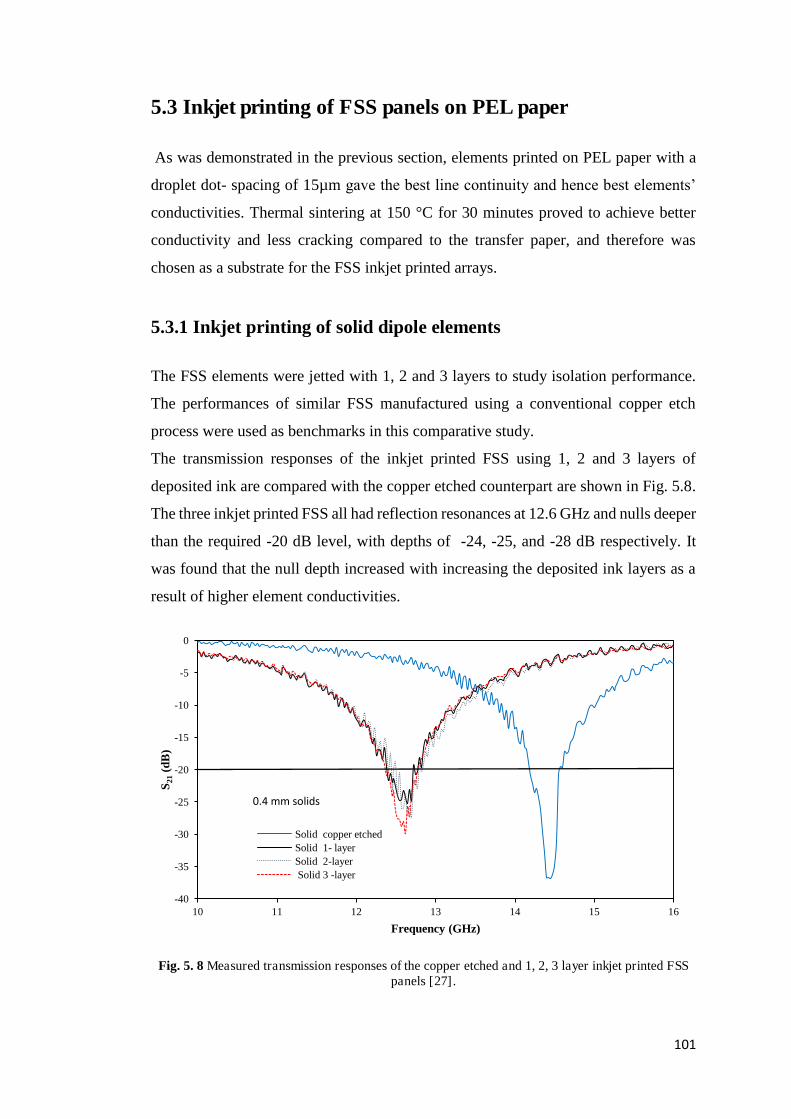
101
5.3 Inkjet printing of FSS panels on PEL paper
As was demonstrated in the previous section, elements printed on PEL paper with a
droplet dot- spacing of 15µm gave the best line continuity and hence best elements’
conductivities. Thermal sintering at 150 °C for 30 minutes proved to achieve better
conductivity and less cracking compared to the transfer paper, and therefore was
chosen as a substrate for the FSS inkjet printed arrays.
5.3.1 Inkjet printing of solid dipole elements
The FSS elements were jetted with 1, 2 and 3 layers to study isolation performance.
The performances of similar FSS manufactured using a conventional copper etch
process were used as benchmarks in this comparative study.
The transmission responses of the inkjet printed FSS using 1, 2 and 3 layers of
deposited ink are compared with the copper etched counterpart are shown in Fig. 5.8.
The three inkjet printed FSS all had reflection resonances at 12.6 GHz and nulls deeper
than the required -20 dB level, with depths of -24, -25, and -28 dB respectively. It
was found that the null depth increased with increasing the deposited ink layers as a
result of higher element conductivities.
Fig. 5. 8 Measured transmission responses of the copper etched and 1, 2, 3 layer inkjet printed FSS panels [27].
10 11 12 13 14 15 16-40
-35
-30
-25
-20
-15
-10
-5
0
Frequency (GHz)
S 21(d
B)
0.4 mm solids
Solid copper etchedSolid 1- layer Solid 2-layer Solid 3 -layer

102
The displacement in frequency of the transmission nulls between the copper etched on
Mylar (0.045 mm thick) and inkjet printed FSS on PEL (0.2 mm thick) was about
1.9 GHz. The effect of substrate thickness ( どどねの 蝦 どに mm), permittivity 鉛嘆 岫 にの 蝦 ね岻, dipole width, conductor thickness and conductor conductivity have
been investigated using CST Microwave Studio™ (CST MWS™). As shown in
Figs. 5.9 (a) and (b), the substrate thickness was found to dominate the null frequency
shift with a displacement corresponding to 88% of the 1.9 GHz change in null
frequency, while the permittivity alone gave a 6% change. If the trends in the two
diagrams are regarded as linear, the resonant frequency was found to have approximate
sensitivities of 9.0 GHz/mm and 0.2 GHz for a change of 1.0 in 鉛嘆 respectively, for
substrate height and permittivity. The other parameters combined caused only a further
6% change in the null frequency.
(a) Substrate thickness vs. Resonant frequency (香追 噺 ぬの岻
(b) Substrate Permittivity vs. Resonant frequency (substrate thickness =0.2 mm) Fig. 5.9 Effect of various substrate (a) thickness, and (b) permittivity, on the array resonant
frequency. The broken curves show the best fit trends [27]
12
12.5
13
13.5
14
14.5
15
0 0.05 0.1 0.15 0.2 0.25 0.3
Fre
quen
cy (
GH
z)
Substrate Thickness (mm)
12
12.5
13
13.5
14
14.5
15
2.5 3 3.5 4 4.5 5 5.5 6 6.5
Fre
quen
cy (
GH
z)
ir

103
5.3.2 Frame dipole elements
It is well known that high frequency induced surface currents tend to concentrate
toward the edges of strip conductors. Consequently, in order to reduce the quantity of
ink required while providing thicker conductors where current flow is high, the precise
features that can be achieved by inkjet printing were utilized to produce frame dipoles,
where conductors are deposited only at the edges as shown in Figs. 5.10 [28]. These
elements were considered to be potentially useful in as much as they would reduce the
quantity of ink required in manufacture, and hence the total overall cost.
(a) Solid dipoles
(b) Frame dipoles
Fig. 5.10 Surface current induced in (a) solid and (b) frame dipole elements at 12.8 GHz [27]
Fw
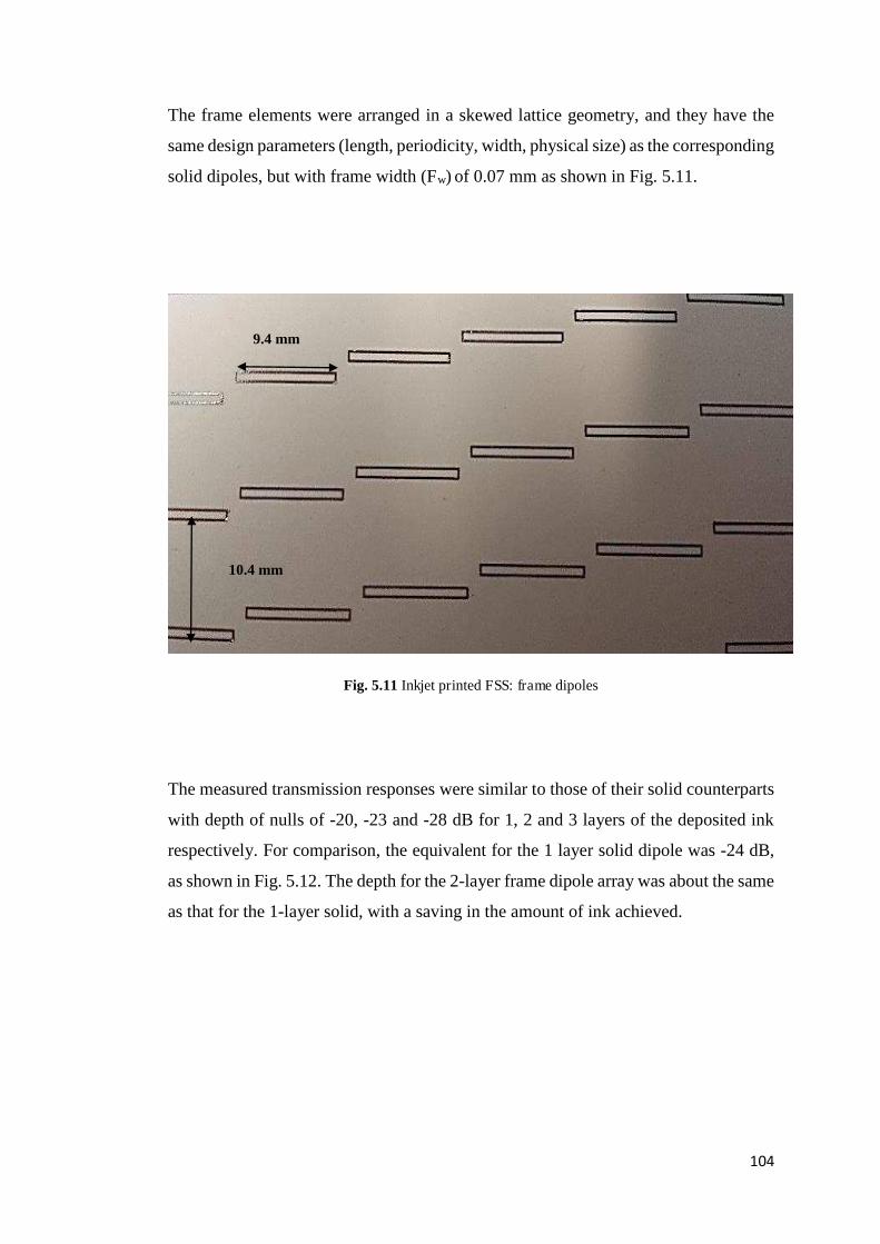
104
The frame elements were arranged in a skewed lattice geometry, and they have the
same design parameters (length, periodicity, width, physical size) as the corresponding
solid dipoles, but with frame width (Fw) of 0.07 mm as shown in Fig. 5.11.
Fig. 5.11 Inkjet printed FSS: frame dipoles
The measured transmission responses were similar to those of their solid counterparts
with depth of nulls of -20, -23 and -28 dB for 1, 2 and 3 layers of the deposited ink
respectively. For comparison, the equivalent for the 1 layer solid dipole was -24 dB,
as shown in Fig. 5.12. The depth for the 2-layer frame dipole array was about the same
as that for the 1-layer solid, with a saving in the amount of ink achieved.
10.4 mm
9.4 mm

105
Fig. 5.12 Measured transmission responses: inkjet printed Solid and Frame dipole FSS [27]
In order to evaluate the performance of the frame dipoles by comparing them with
their copper etched counterparts, the elements were redesigned, with the solid dipole
width w = 1 mm and the frames with widths (FW) of 0.15 and 0.2 mm. This was to
meet the requirements of our copper etching facilities, where the minimum dimensions
that could be etched are of about 0.1 mm. Fig. 5.13 shows the measured transmission
responses of the copper clad etched FSS of 1 mm width solid dipole arrays and the 0.2
and 0.15 mm frame arrays.
Fig. 5.13 Measured transmission responses: copper clad etched Solid and Frame dipole FSS [28]
10 11 12 13 14 15 16-40
-35
-30
-25
-20
-15
-10
-5
0
Frequency (GHz)
S 21(d
B)
Solid 1-layerFrame 1-layerFrame 2-layerFrame 3-layer
-40
-35
-30
-25
-20
-15
-10
-5
0
10 11 12 13 14 15 16 17 18 19 20
S 21(d
B)
Frequency (GHz)
Solid dipoles
Frame dipoles Fw=0.15mm
Frame dipoles Fw=0.2mm
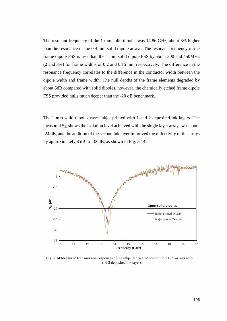
106
The resonant frequency of the 1 mm solid dipoles was 14.86 GHz, about 3% higher
than the resonance of the 0.4 mm solid dipole arrays. The resonant frequency of the
frame dipole FSS is less than the 1 mm solid dipole FSS by about 300 and 450MHz
(2 and 3%) for frame widths of 0.2 and 0.15 mm respectively. The difference in the
resonance frequency correlates to the difference in the conductor width between the
dipole width and frame width. The null depths of the frame elements degraded by
about 5dB compared with solid dipoles, however, the chemically etched frame dipole
FSS provided nulls much deeper than the -20 dB benchmark.
The 1 mm solid dipoles were inkjet printed with 1 and 2 deposited ink layers. The
measured S21 shows the isolation level achieved with the single layer arrays was about
-24 dB, and the addition of the second ink layer improved the reflectivity of the arrays
by approximately 8 dB to -32 dB, as shown in Fig. 5.14.
Fig. 5.14 Measured transmission responses of the inkjet fabricated solid dipole FSS arrays with: 1 and 2 deposited ink layers
10 11 12 13 14 15 16 17 18 19 20-35
-30
-25
-20
-15
-10
-5
0
Frequency (GHz)
S 21(d
B)
1mm solid dipoles
Inkjet printed 1xlayer
inkjet printed 2xlayers

107
The single-layer inkjet printed 0.15 and 0.2 mm frame arrays showed a reduction of
about 3 – 4 dB in the depth, compared with the 1- layer printed solid dipole FSS,
whereas, for the 2- layer 0.15 mm frames it increased by about 4dB, as illustrated in
Fig. 5.15. This improvement in the response of the FSS was obtained whilst achieving
a roughly 50% saving in ink usage when comparing the printed single layer 0.15 mm
frame dipole FSS with the solid dipoles.
Fig. 5.15 Measured transmission responses of the inkjet fabricated solid and frame FSS arrays with: 1 and 2 deposited ink layers
These results are very encouraging and reflect one of the major advantages of inkjet
printing as a fabrication tool. There was also a small reduction in the resonance
frequency, similar to the etched counterparts, of about 3.7% in the case of the single
layer 0.15 mm frame width compared with the solid dipole. This is linked to the lower
quantity of conductor, which led to a slightly higher dipole resistance. An element
resistance study of the inkjet printed FSS is discussed in Section 5.6.
10 11 12 13 14 15 16-35
-30
-25
-20
-15
-10
-5
0
Frequency (GHz)
S 21(d
B)
1mm Solid 1-layer
1mm Solid 2-layer
0.15mm Frame 1-layer
0.15mm Frame 2-layer
0.2mm Frame 1-layer
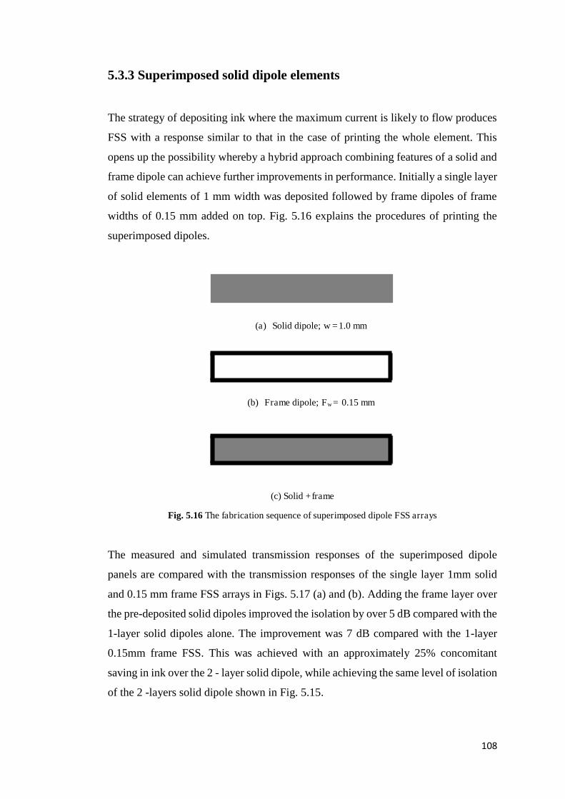
108
5.3.3 Superimposed solid dipole elements
The strategy of depositing ink where the maximum current is likely to flow produces
FSS with a response similar to that in the case of printing the whole element. This
opens up the possibility whereby a hybrid approach combining features of a solid and
frame dipole can achieve further improvements in performance. Initially a single layer
of solid elements of 1 mm width was deposited followed by frame dipoles of frame
widths of 0.15 mm added on top. Fig. 5.16 explains the procedures of printing the
superimposed dipoles.
(a) Solid dipole; w =1.0 mm
(b) Frame dipole; Fw = 0.15 mm
(c) Solid +frame
Fig. 5.16 The fabrication sequence of superimposed dipole FSS arrays
The measured and simulated transmission responses of the superimposed dipole
panels are compared with the transmission responses of the single layer 1mm solid
and 0.15 mm frame FSS arrays in Figs. 5.17 (a) and (b). Adding the frame layer over
the pre-deposited solid dipoles improved the isolation by over 5 dB compared with the
1-layer solid dipoles alone. The improvement was 7 dB compared with the 1-layer
0.15mm frame FSS. This was achieved with an approximately 25% concomitant
saving in ink over the 2 - layer solid dipole, while achieving the same level of isolation
of the 2 -layers solid dipole shown in Fig. 5.15.

109
(a) Measured S21 (dB)
(b) Simulated S21 (dB)
Fig. 5.17 Transmission responses S21 of: 1-layer solid dipoles, 1-layer frame dipoles are compared with depositing frames on top of pre-deposited dipoles, (a) measured, and (b) simulated
10 11 12 13 14 15 16 17 18 19 20-40
-35
-30
-25
-20
-15
-10
-5
0
Frequency (GHz)
S 21(d
B)
1mm Solid 1-layer
0.15mm Frame 1-layer
Solid + Frame
-40
-35
-30
-25
-20
-15
-10
-5
0
10 11 12 13 14 15 16 17 18 19 20
S 21(d
B)
Frequency (GHz)
Solid dipole
Frame dipole
Solid + frames

110
5.4 Printing defects
During the printing process some imperfections in the edge definitions and also defects
in the elements were observed as shown in Fig. 5.18 and Fig. 5.19. The edge of the
dipole element in Fig. 5.18 (a) has some discontinuities generated during the
deposition of the first layer of the ink. These discontinuities were infilled by the
addition of the second layer, resulting in more well-defined edges, as shown in
Fig. 5.18 (b).
Defects such as horizontal cuts and non-linearity in the vertical edges depicted in
Fig. 5.19 (a) were observed in very few of the 0.2 mm frame dipole elements. The
horizontal cuts are caused by total or partial blockage of the printing nozzles, which
results in separation in the dipole shapes, influencing the FSS performance at the
frequency of operation, particularly if those defects are more than 20% of the total
number of elements, as reported in [14].
The non-linear outlines of the vertical edges are more apparent in the frame dipoles,
as they are thinner than the solid dipoles. Such phenomena could increase the element
electrical resistance leading to reduction in the FSS reflectivity, which might lead to a
transmission response level (S21) less than the benchmark of -20 dB. However, this
issue could also be resolved by the addition of a second ink layer as shown in
Fig. 5.19 (b).
(a) 1-layer (b) 2-layer
Fig. 5.18 1mm inkjet printed solid dipole FSS (a) 1-layer of deposited ink (b) 2-layer of deposited ink [27]
1 mm

111
(a) 1-layer
(b) 2-layer
Fig. 5.19 0.2 mm inkjet printed frame dipole FSS (a) 1- layer of deposited ink (b) 2-layer of deposited ink [27]

112
Further errors were observed during the production of the printed FSS solid dipole
elements, expected to be caused by full or partial blockage in the printing nozzles, as
shown in Fig. 5.20. Some of those errors led to the dipoles being divided into 2 or more
elements, as a result of either horizontal or vertical cuts [29]. Figs. 5.20 (b) and (d)
show the effect of a spurious line generated by ink spray resulting from a partially
blocked nozzle.
(a) (b)
(c) (d) Fig. 5.20 Defective dipole elements: (a) dipole with a slot, (b) dipole with two sprayed edge lines,
(c) dipole with Horizontal gaps and (d) misaligned dipole with horizontal gaps [29].
The defective dipoles observed were modelled in CST Microwave Studio® and in order
to simplify the simulation, periodic boundaries were used so that all elements suffered
the same defect. This represents a worst case scenario, unlike the study of defects
presented in Chapter 4. Dipoles with 9.4mm length, 1mm width were arranged in a
square lattice geometry with a periodicity of 10.4 mm. Fig. 5.21 shows some of the
modelled printing error scenarios.

113
(a) Dipole with 0.1mm horizontal gaps
(b) Dipole with 0.2mm horizontal gap and misallignment
(c) Dipole with dots caused by edge spray
(d) Dipole with two edge lines caused by spray
(e) Dipole with a slot (slot width varies from 0.1 to 0.7mm)
(f) Dipole with horizontal gap; (gap width 0.01 to 0.8 mm)
(g) Dipole with vertical gap; (gap width 0.005 to 1 mm)
Fig. 5.21 Modelled dipole FSS printing errors [29]
The simulated resonance frequency (fr) of the perfect dipole FSS array was about
11.42 GHz. The introduction of the horizontal gaps of widths of 0.1, and 0.2 mm shown
in Figs. 5.21 (a) and (b), which may result from a blocked nozzle, results in increasing
fr by 30 and 60 MHz respectively.

114
(a) Resonance frequency vs. Slot width
(b) Resonance frequency vs. horizontal gap width
(c) Resonance frequency vs. vertical gap width
Fig. 5.22 Simulated effect of printing errors in dipole elements on the FSS resonant frequency [29]
11.4
11.45
11.5
11.55
11.6
11.65
11.7
11.75
11.8
11.85
0 0.1 0.2 0.3 0.4 0.5 0.6 0.7 0.8
Fre
quen
cy (
GH
z)
Slot width (mm)
11.4
11.45
11.5
11.55
11.6
11.65
11.7
11.75
11.8
11.85
0 0.1 0.2 0.3 0.4 0.5 0.6 0.7 0.8 0.9
Fre
quen
cy (
GH
z)
Horizontal gap width (mm)
10
12
14
16
18
20
22
24
26
0 0.1 0.2 0.3 0.4 0.5 0.6 0.7 0.8 0.9 1
Fre
quen
cy (
GH
z)
Vertical gap width (mm)

115
Defects described in Figs. 5.21 (c) and (d) represent the ink spray effect as a result of
partially blocked nozzles. The two narrow edge lines (0.1 mm) and the dots (50µm)
around the dipoles caused a modelled decrease in resonant frequency of 350 and 550
MHz (3-5%) respectively. This is a consequence of the capacitive loading that was
produced by those lines. Fig. 5.22 (a) shows the effect of having a slot in the elements
as depicted in Fig. 5.20 (a) and Fig. 5.21 (e). The slot width was varied from 0.1 – 0.7
mm.
The impact of the horizontal and vertical gaps, depicted in Figs. 5.21 (f) and (g), is
shown in Figs. 5.22 (b) and (c), respectively. The width of the introduced horizontal
gap was varied from 0.01 to 0.8 mm, where the vertical gap from 0.005 to 1 mm.
Simulation results show that the vertical gaps have, as might be expected, a greater
impact on the resonance frequency than horizontal gaps and enclosed horizontal slots
within the dipoles. A tiny vertical gap of about 0.005mm in the dipole centres led to an
increase in frequency of about (78%) 9 GHz (Fig. 5.22 (c)) compared with less than
400MHz (3.5%) in the cases of horizontal gaps and enclosed horizontal slots – the
current distribution was seriously affected, as to be expected. However, all of the errors
presented could have a severe impact on highly convoluted elements as the two
dimensional nature of these designs, such as in Chapter 6, means that horizontal defects
could also disturb the current flow.

116
5.5 Dimensions of the inkjet printed panels
It was noticed that the inkjet printed solid and frame FSS elements were slightly wider
than the equivalent chemically etched FSS elements owing to drop spreading on the
paper substrate, but there was little difference in the length as summarized in
Table. 5.1. The size of the distance between the adjacent droplets influences the width
of the printed elements, with element width increasing for decreased drop spacing.
Additionally, the deposition of multiple layers also increases the dipole width due to
the extra amount of jetted ink spreading on the supporting substrate, as illustrated in
Fig. 5.23. The shape of the printed elements was a coffee ring shape, similar to the
droplet spreading behaviour on the supporting substrates that was reported in [20],
[21].
Fig. 5.23 Effects of different drop spacing and multiple layer deposition on the width and height of the
printed element profile
0
1
2
3
4
5
6
7
8
0 100 200 300 400 500 600 700 800 900
Hei
ght (
µm
)
Width (µm)
1- layer, DS =20µm2- layer, DS =20µm3- layer, DS =20µm1- layer, DS =15µm2- layer, DS =15µm3- layer, DS =15µm

117
The increase in the width of the element is more noticeable for the frame dipole
elements, as they are more sensitive to the droplet spreading effect, as the droplets
would spread on both sides of the frame’s arms. In the case of the solid dipole elements
the spreading was proportionally less significant as droplets will be overlapping with
the adjacent ink droplets. Furthermore it was noticed that the ink spreading is
inhomogeneous in both frame arms. Fig. 5.24 shows a micrographic of one frame
dipole element where the upper and lower arms of the frame had widths of 121, and
143 µm respectively. Similarly, additional deposited ink layers also tend to increase
the element widths as well as thickness, as more droplets are deposited.
Fig. 5.24 Microscopic image; difference in the 70µm 2- layers frame element arms

118
TABLE. 5. 1 INKJET PRINTED FSS: DIFFERENCE IN WIDTH AND LENGTH COMPARED WITH THE
CHEMICALLY ETCHED FSS COUNTERPARTS [27]
Sample
Width (mm)
Ink
Layer
Avg Width
(mm) 〉w %
Avg Length
(mm) 〉L %
0.07 (F)
1 0.118 68.5 9.41 0.1
2 0.121 72.8 9.43 0.3
3 0.155 121 9.45 0.5
0.4 (S)
1 0.41 2.5 9.38 -0.2
2 0.46 15 9.42 0.2
3 0.53 32 9.44 0.4
1 (S) 1 1.05 5 9.41 0.1
2 1.188 18.8 9.41 0.1
0.2 (F) 1 0.27 35 9.39 -0.1
2 0.32 60 9.4 0
0.15 (F) 1 0.21 40 9.41 0.1
2 0.25 66.6 9.43 0.3
1 (S) +0.15(F) 1+1 1.077 7.7 9.42 0.2
(S) Solid dipoles, (F) Frame dipoles

119
5.6 Resistance study
This section investigates the dc point-to-point resistance of the 15 FSS samples
considered in Section 5.3 (solid, frame, and superimposed dipoles), and later the FSS
samples from Sections 5.2.1 and 5.2.2 that were treated with different sintering
techniques. The resistance measurements were carried out using a digital multi-meter
measuring every individual element of the 374 elements in each of the FSS arrays.
Figs. 5.25 (a) and (b) compare the transmission responses S21, and overall average
resistance values in Ohms for the 0.4 mm solid and 70 µm frame dipole FSS
respectively.
The depth of the transmission null increases as the number of the deposited ink layers
increases for the frame and solid dipole FSS, and the resistance values decrease
accordingly, as shown in Figs. 5.25 (a) and (b) respectively. The null depth of the
2-layer frame dipole improved from the minimum acceptable level of -20 dB of the
1-layer frame to -23 dB, which is exactly the response of the 1-layer solid dipole while
still saving in ink. In addition, the deposition of the 70 µm frame on top of the 1-layer
solid dipoles has improved the S21 response by about 3 dB.
The 2nd deposited layer of ink has reduced the total average resistance of the frame
dipole FSS by 6Ω, from 13.5 to 7.5 Ω, and by about 1 Ω in the case of the solid dipoles.
This reflects the improvement in the null depth as shown in Fig. 5.25 (a). The total
average resistance of the solid + frame FSS is also less than the total average resistance
of the 1-layer solid dipoles by 1 Ω.
Figs. 5.26 (a) and (b) compare the transmission nulls and total average resistances of
the FSS with wider elements: the 1 mm solid and 0.15 and 0.2 mm frame dipoles. The
impact of depositing more layers has the same positive effect on the depth of nulls and
reduces the average total resistance of the arrays, as in the above case of the 0.4
mm solid and 70 µm frame dipole FSS. However, overall average resistances of the
1mm solid, 0.15 and 0.2 mm frames are less than their 0.4 mm solid and 70 µm

120
counterparts. This is a result of the fact that they have more deposited ink as they are
wider.
(a) Comparison of transmission null depths S21
(b) Comparison of resistance values
Fig. 5.25 Measured transmission responses (a) and resistance values (b) of the 0.4mm solid and 70µm frame dipole FSS [27]
15
17
19
21
23
25
27
29
Frame1-layer
Frame2-layer
Frame3-layer
Solid1-layer
Solid2-layer
Solid3-layer
Solid 1-layer+Frame 1-layer
S 21(-
dB)
FSS Sample
0
2
4
6
8
10
12
14
16
Frame1-layer
Frame2-layer
Frame3-layer
Solid1-layer
Solid2-layer
Solid3-layer
Solid 1-layer+Frame 1-layer
Res
ista
nce
(Ω)
FSS Samples

121
(a) Comparison of transmission null depths S21
(b) Comparison of resistance values
Fig. 5. 26 Measured transmission responses (a) and resistance values (b) of the 1mm solid and 0.15 and 0.2 mm frame dipole FSS [27]
15
17
19
21
23
25
27
29
31
0.15 Frame1-layer
0.15 Fame2-layer
0.2 Frame1-layer
0.2 Frame2-layer
Solid1-layer
Solid2-layer
Solid + 0.15Frame
Solid + 0.2Frame
S 21(
-dB
)
FSS Samples
0
1
2
3
4
5
6
7
8
9
0.15 Frame1-layer
0.15 Fame2-layer
0.2 Frame1-layer
0.2 Frame2-layer
Solid1-layer
Solid2-layer
Solid + 0.15Frame
Solid + 0.2Frame
Res
ista
nce
(Ω)
FSS Samples

122
This improvement in the conductivity of the elements also results in deeper nulls in
comparison with the 0.4 mm width FSS. The measured resistance values are
summarised in Table. 5.2 [27].
TABLE. 5. 2 MEASURED RESISTANCE
Layer 1
Width (mm)
Layer 2
Width-(mm)
R
(Ω)
Standard
deviation
solid 0.4 - - 4.3 0.5
solid 0.4 solid 0.4 3.1 0.8
frame 0.070 - - 13.5 2
frame 0.07 frame 0.07 7.5 1.9
solid 0.4 frame 0.07 3.2 0.5
solid 1 - - 4 0.6
solid 1 solid 1 0.9 0.13
frame 0.15 - - 8.2 1.3
frame 0.15 frame 0.15 3.1 0.5
frame 0.2 - - 6.3 1
frame 0.2 frame 0.2 2.5 0.6
solid 1 frame 0.15 1.9 0.3
solid 1 frame 0.2 1.1 0.3
FSS arrays with higher average resistance than 13.5 Ω did not achieve the required
transmission response, as illustrated in Fig. 5.27. The transmission response falls
below the 20 dB isolation level as the resistance increases beyond 13.5 Ω. The arrays
presented in Sections 5.2.1 and 5.2.2 that were printed on transfer paper had high

123
average resistances except the FSS arrays that were made with 15 µm drop spacing. It
was found that those arrays suffered from severe discontinuities and cracks. Some
were completely nonconductive, especially those that were sintered with IPL due to
the damage that occurred to the transfer paper substrate, as was described in
Section 5.2.2. Table. 5.3 summarises the dc point -to-point resistances and the amount
of printing errors of the FSS panels presented in Sections 5.2.1 and 5.2.2 with their S21
performances. The FSS panel printed on transfer paper and sintered with IPL, had an
average resistance of about 36 Ω. However, it had an S21 of about -1 dB in comparison
to -8 dB in the case of the arrays that were sintered thermally with average resistance
of 42 Ω. That was due to the difference in the amount of defects which was 90% and
38%, respectively, as shown in Table. 5.3. The estimated printed FSS screens element
conductivity was about 蛤 2 to 4% of bulk silver conductivity in the case of single ink
layer. For instance, the frame dipole elements had an average conductivity of 2% of
bulk silver, therefore, two layers of deposited ink were needed to meet the required
skin depth.
Fig. 5.27 Elements average resistance vs. transmission response
-35
-30
-25
-20
-15
-10
-5
0
0 5 10 15 20 25 30 35 40 45 50
S 21(
dB
)
Average resistance (Ω)

124
TABLE. 5. 3 SUMMARY OF THE MEASURED RESISTANCES OF THE FSS PANELS FROM SECTIONS 5.2.1 AND 5.2.2
Sintering
technique
Substrate
type
Dot
spacing
(µm)
Ink layers S21
(dB)
R
(Ω)
Errors
(%)
Standard
deviation
Photonics
(few secs)
Tattoo 25 1 -1 36 90 41
Photonics
(few secs)
Tattoo 20 1 -10 24 24 22
Photonics
(few secs)
PEL 20 1 -21 11 0 0.9
Plasma
(30 mins)
PEL 20 1 -20 7.7 0.8 1.2
Plasma
(30 mins)
PEL 20 2 -22 5.6 0.3 0.6
Thermal
(135 Cゼ, 30 mins)
Tattoo 20 1 -8 42.2 38 59
Thermal
(135 Cゼ, 30 mins)
Tattoo 15 1 -21 11 0 4
Thermal
(135 Cゼ, 30 mins)
PEL 20 1 -17 16 0 1.1
Thermal
(135 Cゼ, 45 mins)
PEL 20 1 -20 11 0 1.3
Thermal
(135 Cゼ, 60 mins)
PEL 20 1 -22 10 0 0.5
Thermal
(150 Cゼ, 30 mins)
PEL 15 1 -24 3.1 0 0.6

125
5.7 Conclusion
This chapter investigates factors that contribute to the inkjet manufacture of frequency
selective surfaces with acceptable levels of performance. Silver nanoparticle inks were
deposited on environmentally friendly paper substrates, as might be used in improving
the signal – to – interference ratio and user privacy in the built environment. The study
focused on dipole element configurations. Trials of FSS panels treated with three
different sintering techniques were made. The principal performance indicator was the
depth of the null in the array transmission/frequency response – a measure of the
isolation obtainable. FSS panels printed on tattoo paper and treated with plasma and
flash photonic sintering suffered from severe cracking which led to poor levels of
isolation due to the high number of non-conductive or high resistive elements.
However, arrays printed on PEL papers proved to provide better quality FSS screens
with all three sintering techniques mentioned.
Studying the influence of the number of deposited ink layers, together with the ability
to deposit droplets on demand allowed modification of the array element design in
ways which reduced the amount of deposited conducting material, whilst still
achieving the satisfactory benchmark level of isolation of 20 dB. In frame dipoles, the
ink is deposited only at the edges, where the surface current amplitude is maximimum.
Such modifications allow savings in ink of about 50% while achieving the required
level of isolation of 20 dB in, for example, the case of the single layer frame arrays of
just 70 µm frame width [27]. These are difficult to fabricate with conventional
subtractive methods. Further modifications to the elements have also been considered,
where an extra frame layer was superimposed on a layer of solid dipole elements. This
approach, viable only with inkjet printing, improved the isolation level of the FSS by
approximately 7 dB relative to that of the 1-layer solid dipole FSS alone. It achieved
the same level as that of the corresponding 2-layer solid dipole arrays whilst saving
25% of the ink deposited.
Deposited thin lines are prone to discontinuities, especially in the case of the frame
elements used for example in thin paper. The effect of such discontinuities were

126
mitigated by the addition of an extra layer of ink, raising the possibility of repairing
defective elements, which is unlikely to be possible with conventional subtractive
fabrication techniques.
In addition, the arrays were also assessed in terms of their average dc point – to –point
element resistance and related to the level of isolation obtained; the highest average
resistance to accomplish the benchmark isolation level was 13.5 Ω, that in the case of
the 70 µm frames, whereas the lowest resistance observed in this study was 0.λ Ω
achieving a level of isolation of 31 dB in the case of the 2-layer, 1 mm wide, solid
arrays.
The theme of this study is continuing, with similar investigations applied to complex
convoluted element structures [30], [31] in Chapter 6.

127
References
[1] M. Philippakis, C. Martel, D. Kemp, S. Appleton, R. Pearson, and E. A. Parker, “Application of FSS Structures to Selectively Control the Propagation of signals into and out of buildings, Annex 3,” Ofcom ref AY4464, pp. 1–54, 2004.
[2] P. S. Taylor, A. C. M. Austin, E. A. Parker, M. J. Neve, J. C. Batchelor, J. T.-P. Yiin, M. Leung, G. B. Rowe, A. G. Williamson, and K. W. Sowerby, “Angular independent frequency selective surfaces for interference control in indoor wireless environments,” Electron. Lett., vol. 48, no. 2, p. 61, 2012.
[3] G. Sung, K. Sowerby, M. Neve, and A. Williamson, “A Frequency-Selective Wall for Interference Reduction in Wireless Indoor Environments,” IEEE Antennas Propag. Mag., vol. 48, no. 5, pp. 29–37, Oct. 2006.
[4] J. C. Batchelor, E. A. Parker, J. A. Miller, V. Sanchez-Romaguera, and S. G. Yeates, “Inkjet printing of frequency selective surfaces,” Electron. Lett., vol. 45, no. 1, p. 7, 2009.
[5] W. G. Whittow, Y. Li, R. Torah, K. Yang, S. Beeby, and J. Tudor, “Printed frequency selective surfaces on textile,” Electron. Lett., vol. 49, no. 24, pp. 1507–1509, 2013.
[6] E. Arnaud, A. Kanso, T. Monediere, D. Passerieux, M. Thevenot, E. Beaudrouet, C. Dossou-yovo, and R. Noguera, “Inkjet printing of frequency selective surfaces on EBG antenna radome,” in 2012 6th European Conference on Antennas and Propagation (EUCAP), 2012, pp. 2693–2696.
[7] B. Derby, “Inkjet Printing of Functional and Structural Materials: Fluid Property Requirements, Feature Stability, and Resolution,” Annu. Rev. Mater. Res., vol. 40, pp. 395–414, 2010.
[8] B. J. Perelaer, A. W. M. de Laat, C. E. Hendriks, and U. S. Schubert, “Inkjet-printed silver tracks: low temperature curing and thermal stability investigation,” J. Mater. Chem., vol. 18, p. 3209, 2008.
[9] G. Shaker, A. Rida, S. Safavi-Naeini, M. M. Tentzeris, and S. Nikolaou, “Inkjet printing of UWB antennas on paper based substrates,” Antennas Wirel. Propag. Lett. IEEE, vol. 10, pp. 111 – 114, 2011.
[10] V. Sanchez-Romaguera, M. a. Ziai, D. Oyeka, S. Barbosa, J. S. R. Wheeler, J. C. Batchelor, E. a. Parker, and S. G. Yeates, “Towards inkjet-printed low cost passive UHF RFID skin mounted tattoo paper tags based on silver nanoparticle inks,” J. Mater. Chem. C, vol. 1, no. 39, p. 6395, 2013.
[11] D. J. Lee, J. H. Oh, and H. S. Bae, “Crack formation and substrate effects on electrical resistivity of inkjet-printed Ag lines,” Mater. Lett., vol. 64, no. 9, pp. 1069–1072, 2010.
[12] J. H. Song and H. M. Nur, “Defects and prevention in ceramic components

128
fabricated by inkjet printing,” J. Mater. Process. Technol., vol. 155–156, pp. 1286–1292, Nov. 2004.
[13] B. M. Turki, E. A. Parker, M. A. Ziai, J. C. Batchelor, V. Sanchez-Romaguera, and S. G. Yeates, “Study of printing errors in digitally fabricated FSS,” in 2013 Loughborough Antennas & Propagation Conference (LAPC), 2013, pp. 429–432.
[14] B. M. Turki, E. A. Parker, J. C. Batchelor, M. A. Ziai, S. G. Yeates, and V. Sanchez-Romaguera, “Influence of defective elements on performance of frequency selective surfaces,” Electron. Lett., vol. 49, no. 17, pp. 1054–1055, Aug. 2013.
[15] S. M. A. Hamdy and E. A. Parker, “Influence of lattice geometry on transmission of electromagnetic waves through arrays of crossed dipoles,” IEE Proc. H Microwaves, Opt. Antennas, vol. 129, no. 1, p. 7, 1982.
[16] “PM000040 Rev. 05, DMP-2800 Series - DMP2800GuideVersion2.0.pdf.” [Online]. Available: http://www.lilliu.co.uk/resources/DMP/DMP2800GuideVersion2.0.pdf. [Accessed: 22-Aug-2015].
[17] “Silver nanoparticle ink <150 nm particle size (DLS), 20 wt. % (dispersion in organic solvents) Sigma-Aldrich.” [Online]. Availableμ http://www.sigmaaldrich.com/catalog/product/aldrich/719048?lang=en®ion=GB. [Accessed: 22-Aug-2015].
[18] “Information Sheet for PEL Nano P60.pdf.” [Online]. Availableμ http://www.printedelectronics.co.uk/Information Sheet for PEL Nano P60.pdf. [Accessed: 22-Aug-2015].
[19] A. M. J. van den Berg, A. W. M. de Laat, P. J. Smith, J. Perelaer, and U. S. Schubert, “Geometric control of inkjet printed features using a gelating polymer,” J. Mater. Chem., vol. 17, no. 7, p. 677, 2007.
[20] R. Deegan, “Pattern formation in drying drops,” Phys. Rev. E, vol. 61, no. 1, pp. 475–485, 2000.
[21] M. Ikegawa and H. Azuma, “Droplet Behaviors on Substrates in Thin-Film Formation Using Ink-Jet Printing,” JSME Int. J. Ser. B, vol. 47, no. 3, pp. 490–496, 2004.
[22] V. Sanchez-Romaguera, S. Wünscher, B. Turki, D. Oyeka, R. Abbel, B. Silvia, T. Daniel J., J. C. Batchelor, E. A. Parker, U. S. Schubert, and S. G. Yeates, “Inkjet printed paper based Frequency Selective Surfaces and on-skin RFID tags; the interrelation between silver nanoparticle ink, paper substrate and low temperature sintering technique selection,” J. Mater. Chem. C, vol. 3, no. 9, pp. 2132–2140, 2015.
[23] V. Sanchez-Romaguera, M. A. Ziai, D. Oyeka, S. Barbosa, J. S. R. Wheeler, J. C. Batchelor, E. A. Parker, and S. G. Yeates, “Towards inkjet-printed low cost passive UHF RFID skin mounted tattoo paper tags based on silver nanoparticle

129
inks,” J. Mater. Chem. C, vol. 1, no. 39, p. 6395, 2013.
[24] H. Andersson, a Manuilskiy, C. Lidenmark, J. Gao, T. Öhlund, S. Forsberg, J. Örtegren, W. Schmidt, and H.-E. Nilsson, “The influence of paper coating content on room temperature sintering of silver nanoparticle ink.,” Nanotechnology, vol. 24, no. 45, p. 455203, 2013.
[25] M. Allen, J. Leppäniemi, M. Vilkman, A. Alastalo, and T. Mattila, “Substrate-facilitated nanoparticle sintering and component interconnection procedure.,” Nanotechnology, vol. 21, no. 47, p. 475204, 2010.
[26] S. Wünscher, R. Abbel, J. Perelaer, and U. S. Schubert, “Progress of alternative sintering approaches of inkjet-printed metal inks and their application for manufacturing of flexible electronic devices,” J. Mater. Chem. C, vol. 2, no. 48, pp. 10232–10261, Sep. 2014.
[27] B. M. Turki, E. A. Parker, S. Wünscher, U. S. Schubert, R. Saunders, V.
Sanchez-romaguera, M. A. Ziai, S. G. Yeates, and J. C. Batchelor, “Significant
Factors in the Inkjet Manufacture of Frequency Selective Surfaces.” Submitted
on June 2015 to IEEE Transactions on Components, packaging and
Manufacturing Technology.
[28] B. M. Turki, E. A. Parker, J. C. Batchelor, M. A. Ziai, S. Wünscher, S. G. Yeates, and U. S. Schubert, “Inkjet Fabrication of Frame Dipole FSS,” in 2014 Loughborough Antennas & Propagation Conference (LAPC), 2014, pp. 347–349.
[29] B. M. Turki, E. A. Parker, R. Saunders, J. Wheeler, S. G. Yeates, and J. C. Batchelor, “Deficiencies in Printed FSS Intended for Application in Smart Buildings,” in Antennas and Propagation & USNC/URSI National Radio Science Meeting, 2015 IEEE International Symposium on, 2015, vol. 2, pp. 320–321.
[30] E. A. Parker and A. N. A. El sheikh, “Convoluted array elements and reduced size unit cells for frequency-selective surfaces,” IEE Proc. H Microwaves, Antennas Propag., vol. 138, no. 1, p. 19, 1991.
[31] E. A. Parker, J. C. Batchelor, R. Chiang, A. G. Williamson, B. Sanz-Izquierdo, M. J. Neve, and K. W. Sowerby, “Frequency selectively screened office incorporating convoluted FSS window,” Electron. Lett., vol. 46, no. 5, p. 317, 2010.

130
CHAPTER 6: INKJET PRINTING OF
CONVOLUTED FSS ELEMENTS
6.1 Introduction
Frequency selective panels can transform conventional buildings into smart building
by selecting the electromagnetic waves that could pass through walls, depending on
the frequency of interest. Different FSS designs could be adopted according to the
desired application ranging from simple dipole arrays, square loops, and ring loops to
highly convoluted and interwoven elements [1]–[10]. The arrays could be in the form
of patch elements, which act as band stop filters blocking electromagnetic waves at
certain frequency bands, or slots of elements acting as band pass filters [11], [12].
These FSS panels should be economical when integrated into various materials. Inkjet
printing technology has recently been considered in manufacturing simple frequency
selective arrays printed on various substrates such as glass, textile, paper based and
polyethylenenapthenate (PEN), providing very similar characteristics to their copper
etched equivalents [13]–[17]. FSS frame elements, ink jetted only where surface
currents were likely to be significant, achieved the benchmark acceptable isolation
level of 20 dB in the case of stop band FSS panel. [17],[18]. Low-cost manufacturing,
however, introduces the possibility of encountering some errors in the printed
elements, which could affect the performance of the FSS panels. Errors such as broken
or totally absent elements occurring at random, or in clusters, and their effects on the
performance of the FSS arrays have been considered in [17], [19]–[21].

131
The aims of this chapter are to manufacture and investigate the performance of inkjet
printed arrays of convoluted element FSS screens for buildings, with the least amount
of deposited ink, maximum required conductivity and acceptable performance. Novel
convoluted square elements (patches and slots) operating at 1 – 3 GHz were inkjet
fabricated and compared with their chemically etched counterparts.
The degree of convolution complexity is also considered while designing the
convoluted elements taking into account the limitations of the printer used, for instance,
such as the print head mechanical movements. The Dimatix DMP-2800 print head
moves in continuous rows in a Cartesian coordinate system, meaning one row must be
completed before proceeding to the next [22],[23]. This could affect the adjacent
droplet interactions, especially in the case of vertical and diagonal lines, leading to
some discontinuities in the printed lines. Therefore, the convoluted square elements
were designed with minimum element convolution while achieving similar figures of
merit to other previously reported convoluted square elements [9]. In addition, the
performance of the convoluted square element arrays was compared with equivalents
such as square loop elements having the same unit-cell area.
This chapter also explores the effects of line definition and width on the performance
of the FSS arrays by analysing the impact of the shapes of the printed lines, and
substrate temperature during printing on the element electrical continuity and
resistance. Two silver nano-particle inks printed on PEL paper substrate were studied
for their line definitions especially in the case of vertical lines (perpendicular to print
head direction). Latter sections in this chapter consider the overall average resistance
of the FSS elements and the effects of errors on the responses.

132
6.2 FSS designs
Three FSS designs were chosen: convoluted squares, semi convoluted squares, and
simple square loops. The FSS arrays were designed with the same periodicity P of
25 mm, element length of 23 mm and conductor width w of 0.2 mm, as shown in
Fig. 6.1. The elements were initially chemically etched on copper clad polyester
substrate with substrate relative permittivity 香追 莞 ぬの and loss tangent 購 噺 どどに. The
physical array size was になど 抜 ぬどど mm2. Each FSS screen contained a total of 80
elements arranged in a square lattice geometry.
(a) (b)
(c)
Fig. 6.1 FSS panels’ designs: (a) Convoluted Squares, (b) semi-convoluted square loops (Maltese cross) and (c) simple square loops arrays
L
W
P

133
The transmission responses of the FSS arrays were measured using two log periodic
antennas swept over a frequency range of 1 – 5 GHz. The designs were also modelled
using CST Microwave Studio® (CST MWS®) in order to compare the simulated and
measured S21 transmission responses. The simulated transmission responses of the
three FSS arrays are compared with measurements in Fig. 6.2 (a) and (b). The
simulation results show good agreement with measurements.
(a) Measured S21
(b) Simulated S21
Fig. 6.2 Transmission responses of the FSS arrays: (a) Measured, (b) Simulated
-35
-30
-25
-20
-15
-10
-5
0
1 1.5 2 2.5 3 3.5 4 4.5 5
S 21 (d
B)
Frequency (GHz)
Simple squares
Convoluted squares
Semi-Convouled squares
-35
-30
-25
-20
-15
-10
-5
0
1 1.5 2 2.5 3 3.5 4 4.5 5
S 21 (d
B)
Frequency (GHz)
Square loop
Convoluted square
Semi-convoluted squares

134
6.2.1 Angular stability
It is known that the convolution of FSS elements improves the stability of FSS array
performance with incident ray angle [24], [25]. Additionally, in a real building
environment, the electromagnetic illumination uniformity across an FSS integrated
into a wall could change significantly due to varied angles of incidence, the wall
curvature, and multipath. For that reason, FSS responses for panels intended for
in-building applications should have good immunity to oblique ray incidence. Some
of the issues related to non-uniform electromagnetic illumination and their effect on
the reflectivity of the FSS screens, especially with the presence of defects were
discussed in Section 4.5 and [20].
(a) Measured S21
(b) Simulated S21
Fig. 6.3 Transmission responses of the convoluted square FSS arrays with oblique angle if incidence: (a) Measured, (b) Simulated
-35
-30
-25
-20
-15
-10
-5
0
1 1.5 2 2.5 3 3.5 4 4.5 5
S 21(d
B)
Frequency (GHz)
王 = 0°王 = 45°
-40
-35
-30
-25
-20
-15
-10
-5
0
1 1.5 2 2.5 3 3.5 4 4.5 5
S 21(d
B)
Frequency (GHz)
王 = 0°
王 = 45°

135
As described in Fig. 6.3, the convoluted squares show good stability to oblique
angle of incidence, with a small shift in the central resonant frequency of only
0.4% at 45° (TE) compared to 3.7% at the case of the equivalent simple square
loops (2.7 – 2.6 GHz) in case of normal incidence and 45° (TE), which suggests
the suitability of this design for use in buildings. The effectiveness of the
convolution process is judged by the figure of merit (そ1/P), which is an indication
of the separation between the first resonance and the grating response, and by the
ratio (L/ そ1) which is the measure of how efficiently the available conductor is used.
Table. 6.1 summarises the figures of merit of the convoluted square in comparison
with the simple square loops, and semi-convoluted squares FSS arrays. The
convoluted square FSS arrays achieved a figure of merit (そ1/P) of about 6.5, very
similar to those of convoluted square arrays (6.8) and first generation Hilbert FSS
arrays (5.9) [9].
TABLE. 6.1 SUMMARY FIGURES OF MERIT FOR THE THREE FSS ARRAY ELEMENTS
Element f1 (GHz) P (mm) Unit cell
area (mm2)
そ1/P そ2/P L/ そ1
Square loop
2.79
25
625
4
1.2
0.8
Semi convoluted
(Maltese cross)
2.26 25 625 5.3 1.9 1
Convoluted
square
1.86 25 625 6.5 2.4 1.2
* そ1 and そ2 are the wavelengths of the 1st and 2nd resonant frequencies

136
6.3 Inkjet fabrication of FSS arrays
The three FSS designs were also inkjet printed using a Dimatix DMP-2800 inkjet
printer [22]. The silver nanoparticle ink (SunTronic U5603 from Sun Chemicals)
consisting of a 20 wt% dispersion of silver nanoparticles was used on PEL Nano-P60
paper (PEL paper) which has an inorganic micro-porous receiving layer [26], [27].
The FSS screens were printed with drop spacing of 15 µm, and thermally treated in a
conventional oven at 150° C for 30 minutes, (reported in Chapter 5 to be the optimal
temperature and sintering time for PEL substrate to achieve the best conductivities).
The elements were also printed with single and double layers of the deposited silver
ink and tested for the benchmark isolation level of 20 dB [21]. The results are reported
in the following sections.
6.3.1 Square loops
Fig. 6.4 compares the transmission responses of the chemically etched and inkjet
printed simple square screens. The arrays with a single layer of deposited ink produced
null depths that did not achieve the required benchmark isolation level being only
-18 dB. This is believed to be caused by a difference in the line width noticed between
the horizontal and vertical arms of the square loops, as shown in Fig. 6.5. This
difference was produced by the different drop interaction with the PEL paper
according to whether the line was produced parallel, or perpendicular to the print head
direction.
The difference in the line width between the vertical and horizontal arms of the square
elements is shown in Fig. 6.5. The horizontal lines seem to be more uniform with
average line width of 316 µm, however, the vertical lines suffered from systematic
shrinking points.

137
Fig. 6.4 Measured transmission responses of the inkjet printed and chemically etched simple square FSS arrays
Fig. 6.5 Microscopic image of the single layer inkjet printed square loops line definitions
It is well known that in many inkjet printers, such as the Diamtix inkjet, the print head
moves unidirectionally, in a 2 D Cartesian coordinate system. The print head advances
from left to right along the first horizontal row (y1), before shifting to the next row (y2)
and repeating the same procedure [23]. This would allow the droplets in the vertical
lines to dry and the solvents to evaporate before the droplet in the next row is
deposited. This leads to ink droplets flowing back into what is known as bulges [23],
-35
-30
-25
-20
-15
-10
-5
0
1 1.5 2 2.5 3 3.5 4 4.5 5
S 21(d
B)
Frequency (GHz)
Copper etched Ink - 1 layer
Ink - 2 layer
2λ0 m
240 m
236 m

138
[28]–[30]. As a consequence, much narrower nodes within the printed tracks will be
formed, which affects the electrical conductivity of the lines.
The number of bulges per printed line is inversely proportional to the drop spacing,
(i.e. the smaller the drop spacing the greater the number of bulges within a line [30]).
This issue is not frequent in the horizontal lines due to the larger number of
overlapping adjacent ink droplets deposited consecutively within one printed row.
As shown in Fig. 6.5, the average widths of the bulges and the narrow nodes are 290,
and 240 µm, respectively; that is about 26 and 76 µm thinner than the horizontal lines.
It was also found that the bulges were repeated on average every 236 µm over the 15
bulges that were observed. This issue was also observed in the case of the FSS arrays
with 2 layers of deposited ink. The average horizontal line width was 412 µm and the
vertical line maximum and minimum average widths were 370 and 277 µm, as shown
in Fig. 6.6.
The addition of a second ink layer improved the null depth by about 9 dB to 27dB,
only 3 dB less than their chemically etched counterparts, Fig. 6.4. The resonant
frequencies (fr) were about 2.74 and 2.82 GHz for the 2 layer inkjet printed and the
chemically etched arrays, respectively, leading to a frequency shift of about 3%.
The average point-to-point dc resistance (corner points) of the FSS elements with
1 and 2 of deposited ink layers were 20.1 and 7.2 Ω, respectively. The resistance values
were measured between two points at the corners of the square elements as illustrated
in Fig. 6.7 (a). In addition, the dc resistance of the vertical and horizontal lines were
individually measured by disconnecting the arms of each square element as shown in
Fig. 6.7 (b) and (c). It was found that there was a difference in the vertical and
horizontal square arm conductivity, for instance in the single layer square elements
FSS screen. The horizontal lines had an average resistance of 16.λ Ω compared with
22.3 Ω for the vertical lines, owing to the non-uniformity in the vertical arm line
definitions. However, the FSS screen with double ink layers, had a much lower
resistance for both vertical and horizontal lines and also the difference between the
two was not as pronounced as for 1 layer, with average resistances of 5.4 and 7.6 Ω
for the horizontal and vertical lines, respectively. This is caused by the fact that the
arrays with 2 layers contain more deposited ink, and thus have thicker and wider lines

139
(due to droplet spreading), as shown in Fig. 6.6. The point to point dc resistance values
are summarised in Table. 6.2.
TABLE. 6.2 SUMMARY OF THE POINT-TO-POINT RESISTANCE MEASUREMENTS OF THE INKJET FABRICATED SQUARE LOOPS FSS ARRAYS
Number of ink
layers
Corner point DC
resistance (Ω)
Horizontal line DC
resistance
(Ω)
Vertical line DC
resistance
(Ω)
1 20.1 16.9 22.3
2 7.2 5.4 7.6
(a) Single ink layer (b) double ink layer
Fig. 6.6 Microscopic images of the inkjet printed square loops vertical line definitions: (a) single and (b) double ink layers
2λ0 m
240 m
370 m
277 m

140
(a) Corner to corner or (loop)
(b) Horizontal lines
(c) Vertical lines
Fig. 6.7 Illustrates the steps of dc resistance measurement of the inkjet printed square elements FSS arrays: (a) corner to corner or (loop), (b) horizontal lines and (c) vertical lines
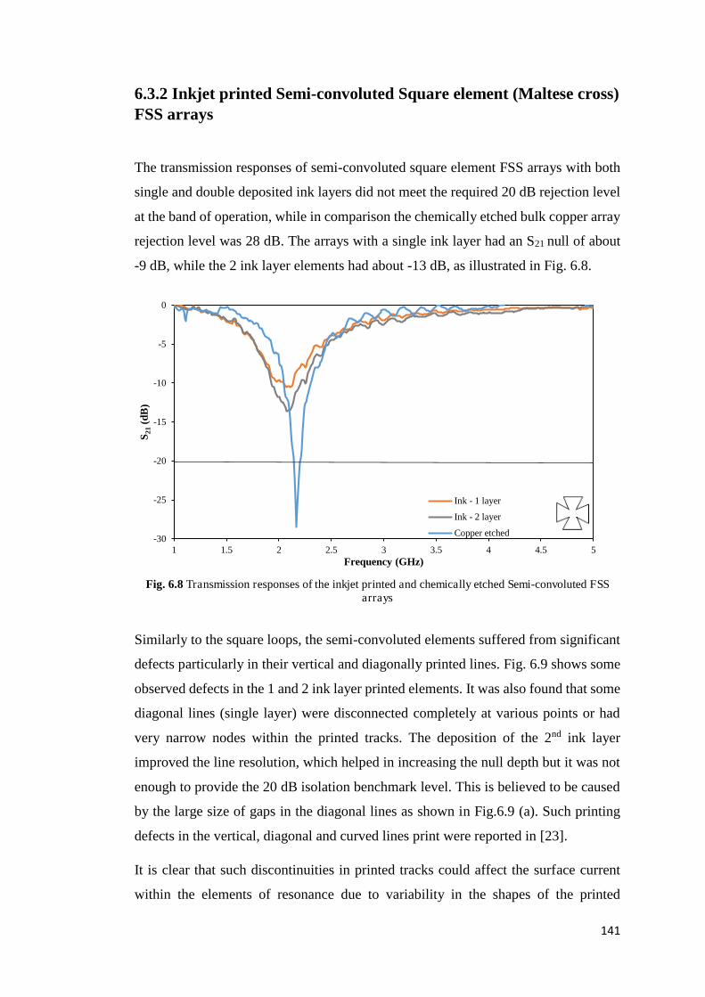
141
6.3.2 Inkjet printed Semi-convoluted Square element (Maltese cross) FSS arrays
The transmission responses of semi-convoluted square element FSS arrays with both
single and double deposited ink layers did not meet the required 20 dB rejection level
at the band of operation, while in comparison the chemically etched bulk copper array
rejection level was 28 dB. The arrays with a single ink layer had an S21 null of about
-9 dB, while the 2 ink layer elements had about -13 dB, as illustrated in Fig. 6.8.
Fig. 6.8 Transmission responses of the inkjet printed and chemically etched Semi-convoluted FSS
arrays
Similarly to the square loops, the semi-convoluted elements suffered from significant
defects particularly in their vertical and diagonally printed lines. Fig. 6.9 shows some
observed defects in the 1 and 2 ink layer printed elements. It was also found that some
diagonal lines (single layer) were disconnected completely at various points or had
very narrow nodes within the printed tracks. The deposition of the 2nd ink layer
improved the line resolution, which helped in increasing the null depth but it was not
enough to provide the 20 dB isolation benchmark level. This is believed to be caused
by the large size of gaps in the diagonal lines as shown in Fig.6.9 (a). Such printing
defects in the vertical, diagonal and curved lines print were reported in [23].
It is clear that such discontinuities in printed tracks could affect the surface current
within the elements of resonance due to variability in the shapes of the printed
-30
-25
-20
-15
-10
-5
0
1 1.5 2 2.5 3 3.5 4 4.5 5
S 21(d
B)
Frequency (GHz)
Ink - 1 layer
Ink - 2 layer
Copper etched

142
elements as a result of these discontinuities. Therefore, the FSS arrays would not
provide a sufficient level of isolation due to the different element conductivities, which
affects the quality of the periodic current distribution across the array.
(a) Single layer
(b) 2 layers
Fig. 6.9 Microscopic photos of the vertical and diagonal lines of (a) single and (b) 2 layers inkjet printed semi-convoluted elements (Maltese cross) FSS arrays
Vertical line
Diagonal line
Diagonal line
Diagonal line
Vertical line
Vertical line

143
6.3.3 Inkjet printed Convoluted Square elements FSS arrays
In common with the semi-convoluted and single layer square elements, the convoluted
square screens did not achieve the benchmark isolation level of 20 dB, as shown in
Fig. 6.10 (a). The printed horizontal track line definitions were stable, however, the
vertical tracks were non-uniform as shown in Fig. 6.10 (b).
(a) Measured transmission responses
(b)Elements microscopic photos (w = 0.2 mm)
Fig. 6.10 Convoluted square elements arrays: (a) 0.2 and 0.4 mm chemically etched and inkjet printed transmission responses in dB, and (b) elements microscopic photo
-35
-30
-25
-20
-15
-10
-5
0
1 1.5 2 2.5 3 3.5 4 4.5 5
S 21(d
B)
Frequency (GHz)
0.2mm 1 layer0.2mm 2layers 15um0.2 mm Copepr0.4mm Copper0.4mm 1 layer 15um

144
The transmission response of the single and double ink layer FSS panels were about
-4, and -7 dB, compared with -30 dB in the case of the chemically etched version, of
Fig. 6.2. The levels of isolation provided by the inkjet panels did not provide sufficient
shielding for in-building applications. In an attempt to improve the performance of
the arrays, the element line width was increased to 0.4 mm. Although the array
reflectivity improved by about 3 dB, the benchmark isolation level was not achieved
with an S21 of only -10 dB for single ink layer, as shown in Fig. 6.10 (a).
In addition, the point-to-point resistance study was conducted on the convoluted
arrays, where the probes were situated at the corners of the elements as shown in
Fig. 6.11. It was found that the 0.2 mm single layer array average dc resistance was
22 Ω, and 33% of the elements were not conductive between the chosen probe
locations. The arrays with 2 layers of ink and the single layer 0.4 mm wide arrays
comprised 5%, and 14% non-conductive elements, respectively, while the average
measured resistances were about 18 and 14 Ω for each case. The convoluted square
elements were also printed with 10 µm drop spacing, though, the printed lines showed
worse line definition, and were discarded from this study.
Fig. 6.11 Point to point dc resistance measurements of the convoluted square elements

145
6.4 Inkjet printed square elements with Silverjet Ink
In another trial to improve the resolution of the printed elements in terms of vertical
line definition and conductivity, an alternative ink was tried, the Silverjet silver
nanoparticle ink (DGP-40LT-15C) from Sigma-Aldrich. This contains 30 – 35% wt
silver dispersion [31], higher than that of the Suntronic silver ink used previously
which was 20%. The new ink was used to jet four of the simple square elements shown
in Fig. 6.1 (c). The designs were deposited at room temperature with a set of line
widths of 0.1 – 1 mm with a 0.1 step, and a single deposited ink layer. The samples
were printed with a droplet spacing of 15 µm and were thermally treated at 150 °C for
30 minutes in a conventional oven.
The point-to-point average dc resistance of the vertical and horizontal arms of the
square elements decreased with the increase in line width, as illustrated in Fig. 6.12.
It was found that at 0.2 mm wide, the vertical and horizontal line resistances were 9
and 8 Ω respectively, about 13 and λ Ω lower than their equivalents printed with the
original Suntronic ink. Furthermore, the dc resistances of the 0.1 mm wide vertical
and horizontal lines printed with the Silverjet ink were 17, and 15.7 Ω, also lower than
the 0.2 mm wide lines printed with the Suntronic silver ink.
Fig. 6.12 Average dc resistance in Ohms vs line width
0
2
4
6
8
10
12
14
16
18
20
22
24
0.1 0.2 0.3 0.4 0.5 0.6 0.7 0.8 0.9 1
R (
Ω)
Line width (mm)
Silverjet ink (Rv)
Silverjet ink (Rh)
SunTronic ink (Rv)
SunTronic ink (Rh)
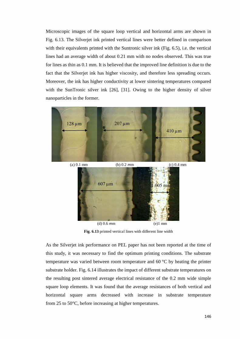
146
Microscopic images of the square loop vertical and horizontal arms are shown in
Fig. 6.13. The Silverjet ink printed vertical lines were better defined in comparison
with their equivalents printed with the Suntronic silver ink (Fig. 6.5), i.e. the vertical
lines had an average width of about 0.21 mm with no nodes observed. This was true
for lines as thin as 0.1 mm. It is believed that the improved line definition is due to the
fact that the Silverjet ink has higher viscosity, and therefore less spreading occurs.
Moreover, the ink has higher conductivity at lower sintering temperatures compared
with the SunTronic silver ink [26], [31]. Owing to the higher density of silver
nanoparticles in the former.
(a) 0.1 mm (b) 0.2 mm (c) 0.4 mm
(d) 0.6 mm (e)1 mm
Fig. 6.13 printed vertical lines with different line width
As the Silverjet ink performance on PEL paper has not been reported at the time of
this study, it was necessary to find the optimum printing conditions. The substrate
temperature was varied between room temperature and 60 °C by heating the printer
substrate holder. Fig. 6.14 illustrates the impact of different substrate temperatures on
the resulting post sintered average electrical resistance of the 0.2 mm wide simple
square loop elements. It was found that the average resistances of both vertical and
horizontal square arms decreased with increase in substrate temperature
from 25 to 50°C, before increasing at higher temperatures.
128 m 207 m
410 m
607 m 1.005 mm

147
Although the difference in the resistance is within the range of 1.4 Ω between the
resistance of the horizontal lines at 50°C and the vertical line at 25°C, it is believed
that it would have a greater impact on the conductivity of complicated convoluted FSS
elements, as the total line lengths will be much longer than 23 mm.
Fig. 6.14 Average dc resistance of printed elements Vs substrate temperature
As a consequence, from this point, all the inkjet printed elements were produced with
silverjet ink with the substrate heated to 50 °C while printing. The estimated
conductivity obtained from square loop elements printed with SunTronic ink was
about 4 and 8 % of bulk silver conductivity for single and double layer deposition,
respectively, in comparison with 13% in the case of SilverJet ink. Therefore, it was
found that two layers of SunTronic ink was needed to meet the skin depth
requirements. This ensures that conductor losses are minimized.
7
7.5
8
8.5
9
9.5
10
25 30 35 40 45 50 55 60
R (
Ω)
Substrate Temperature (ゼC)
Rv RH

148
6.5 Inkjet printed convoluted square elements with Silverjet Ink
The convoluted square elements shown in Fig. 6.1 (a) were reprinted using Silverjet
ink, with line widths of 0.2, 0.4, 0.6, 0.8 and 1mm. However, a change in the
periodicity (P) from 25 to 32 mm was needed in order to allow printed tracks wider
than 0.4 mm. This led to a decrease in the number of the elements within the arrays
from 80 to 54. For comparison, FSS arrays with the same line widths and periodicity
were chemically etched on copper clad polyester. Fig. 6.15 (a) and (b) compare the
transmission responses of both the chemically etched and the inkjet printed convoluted
square elements arrays.
As illustrated in Fig. 6.15 (a), the chemically etched arrays had null depths deeper than
-30 dB with some shift in the resonant frequency due to the variation in the element
line widths. On the contrary, the measured null depths of the inkjet fabricated arrays
varied, where line widths of 0.2, 0.4, 0.6 and 0.8 mm did not achieve the benchmark
rejection level of 20 dB, with null depths of about -9, -12, -14, and -16 dB were
recorded respectively. The 1 mm wide arrays printed with 1 and 2 layers of deposit
ink layers had null depths of -23, -26 dB and achieved the desired isolation level.
Furthermore, the dc point-to-point average resistance indicated in Fig. 6.11 was
carried out on all the 6 inkjet fabricated arrays resulting in the measurements
summarised in Table. 6.3.
Except for the 1mm wide elements, the thinner elements suffered from discontinuities
in their printed tracks with defects of the range of 15 – 25% of the total number of
elements. However, it was found that the 0.2 and 0.4 mm wide tracks had lower
average resistances and defective elements, and thus slightly deeper nulls compared
with the same arrays printed with the original Suntronic silver ink. The 0.2 and
0.4 mm arrays printed with the Suntronic silver nanoparticle ink had average
resistances of 43.4 and 17.6 Ω, about 32 and 12 Ω higher than their counterparts that
were printed with the Sliverjet ink. Fig. 6.16 compares the average measured
resistance in (Ω) with the element line widths in (mm) of the elements printed with
both inks.

149
(a) Chemically etched
(b) Inkjet printed
Fig. 6.15 Measured transmission responses of the convoluted square arrays (P = 32 mm): (a) chemically etched and (b) Inkjet printed
-40
-35
-30
-25
-20
-15
-10
-5
0
1 1.2 1.4 1.6 1.8 2 2.2 2.4
S 21(d
B)
Frequency (GHz)
0.2 mm0.4 mm0.6 mm0.8 mm1 mm
-40
-35
-30
-25
-20
-15
-10
-5
0
1 1.2 1.4 1.6 1.8 2 2.2 2.4
S 21 (d
B)
Frequency (GHz)
0.2 mm
0.4 mm
0.6 mm
0.8 mm
1 mm
1mm 2layer

150
TABLE. 6.3 SUMMARY OF THE POINT-TO-POINT RESISTANCE MEASUREMENTS OF THE INKJET FABRICATED CONVOLUTED SQUARE ELEMENTS FSS ARRAYS
Element line width
(mm)
Number of ink
layers
S21
(dB)
R(Average)
(Ω)
Defective elements
(%)
0.2 1 -9 11.9 17
0.2 (SunTronic Ink) 1 -4 22 33
0.2 (SunTronic Ink) 2 -7 18 5
0.4 (SunTronic Ink) 1 -10 14 14
0.4 1 -12 5.4 15
0.6 1 -14 4.5 25
0.8 1 -16 4.1 20
1 1 -23 3.2 0
1 2 -26 2 1
The arrays were also modelled in CST to compare with the measured transmission
responses of the arrays. Fig. 6.17 (a) shows the simulated S21 results of the copper
etched elements, which showed good agreement with the measured copper etched
arrays results. In the case of the inkjet printed elements, they were modelled with
substrate thickness of 0.2 mm and relative permittivity 香追 莞 ぬの. The value of
conductivity was chosen according to the estimated values from Table 6.3 of about
≈ 14% of bulk silver conductivity.

151
Fig. 6.16 Measured dc point to point resistance Vs elements line widths of ink printed convoluted
square arrays
Simulation of the modelled inkjet arrays in Fig. 6.17 (b) shows that the expected arrays
null depths were deeper than 20 dB benchmark null depth with 24, 28, 30, 32, and
33 dB for the 0.2, 0.4 0.6, 0.8 and 1 mm, respectively. However, these null depths did
not agree with measurements except for the 1 mm elements, which had null depths of
23, and 26 dB for the single and double ink layers, respectively. This is thought to be
caused by the amount of observed defects in the elements which the line width samples
of 0.2 – 0.8 mm suffered from, (up to 25 % in the case of 0.6 mm), as shown in
Table. 6.3. This amount of errors is higher than the tolerable defect level reported in
Chapter 4, and in [19]–[21]. Additionally, it was found that the 1mm single and double
layer convoluted squares conductivities were 15 and 18% of bulk silver conductivity
respectively. Therefore with these conductivities, the skin depth was met by these
samples.
0
5
10
15
20
25
0.2 0.3 0.4 0.5 0.6 0.7 0.8 0.9 1
Ave
rage
res
ista
nce
(Ω)
Line width (mm)
SilverJet
SunTronic

152
(a) copper
(b) Silver ink
Fig. 6.17 Simulated transmission responses results of the modelled inkjet printed convoluted square arrays with periodicity P = 32 mm
-40
-35
-30
-25
-20
-15
-10
-5
0
1 1.2 1.4 1.6 1.8 2 2.2 2.4
S 21(d
B)
Frequency (GHz)
0.2 mm copper
0.4 mm copper
0.6 mm copper
0.8 mm copper
1 mm copper
-40
-35
-30
-25
-20
-15
-10
-5
0
1 1.2 1.4 1.6 1.8 2 2.2 2.4
S 21(d
B)
Frequency (GHz)
0.2 mm ink
0.4 mm ink
0.6 mm ink
0.8 mm ink
1 mm ink

153
6.6 Inkjet printed square elements slot arrays with Silverjet Ink
Slotted versions of the convoluted square FSS were created in order to investigate the
response of inkjet printed slot arrays. It is known that slot arrays act as bandpass filters
passing electromagnetic waves at the resonant frequency [11]. This type of FSS has
not been reported as inkjet printed, presumably because it could be impractical due to
the amount of deposited ink. The aim of this section was to investigate the transmission
responses of slot arrays and the potential defects that might occur. Two slot arrays
were made with slot widths w of 0.2 (P = 25 mm), and 1 mm (P = 32 mm) using the
silverjet silver ink, jetted with 15 µm droplet spacing and treated thermally as stated
previously. The physical size of the arrays was になど 抜 ぬどど mm2, exact complement
of their patch counterparts. The FSS designs were also chemically etched to compare
their transmission responses.
Fig. 6.18 (a) and (b) respectively show the slot configurations of the convoluted square
elements, and the transmission responses of the chemically etched and the inkjet
printed slot arrays. The 0.2 and 1 mm chemically etched copper slot arrays provided
-10 dB pass bands at 1.24 – 2.54 and 1.1 – 2.22 GHz, respectively, while the 1mm
inkjet slotted screen passed 1.08 – 1.96 GHz. The difference in the passband in
comparison to the etched version was due to the difference in the substrate thickness
and permittivity between the PEL paper and polyester substrate. However, the 0.2 mm
inkjet printed slot arrays did not provide any pass band in the frequency range
1 – 5 GHz, which is likely due to ink spreading across the very narrow slots. Hence,
the FSS arrays appeared as a metallic sheet reflecting all frequencies at the band
investigated. Fig. 6.19 (a) and (b) show microscopic images of both the 0.2 and 1 mm
slots.

154
(a)
(b)
Fig. 6.18 Slots of convoluted square elements FSS arrays: (a) Design configuration, and (b) Measured transmission responses of the inkjet printed and chemically etched arrays
It seems that the slots in Fig. 6.19 (a) (red) became filled with ink particularly in the
case of the horizontal slots, where they were obscured by the spreading of the ink
droplets. This is less apparent in the vertical slots, however, they also suffered from
some discontinuities as shown. This suggests that wider slots are needed as these
issues do not exist in the case of the 1 mm slot arrays illustrated in Fig. 6.19 (b).
-40
-35
-30
-25
-20
-15
-10
-5
0
1 1.5 2 2.5 3 3.5 4 4.5 5
S 21(d
B)
Frequency (GHz)
1mm copper
0.2 mm copper
1mm ink
0.2 mm ink
w
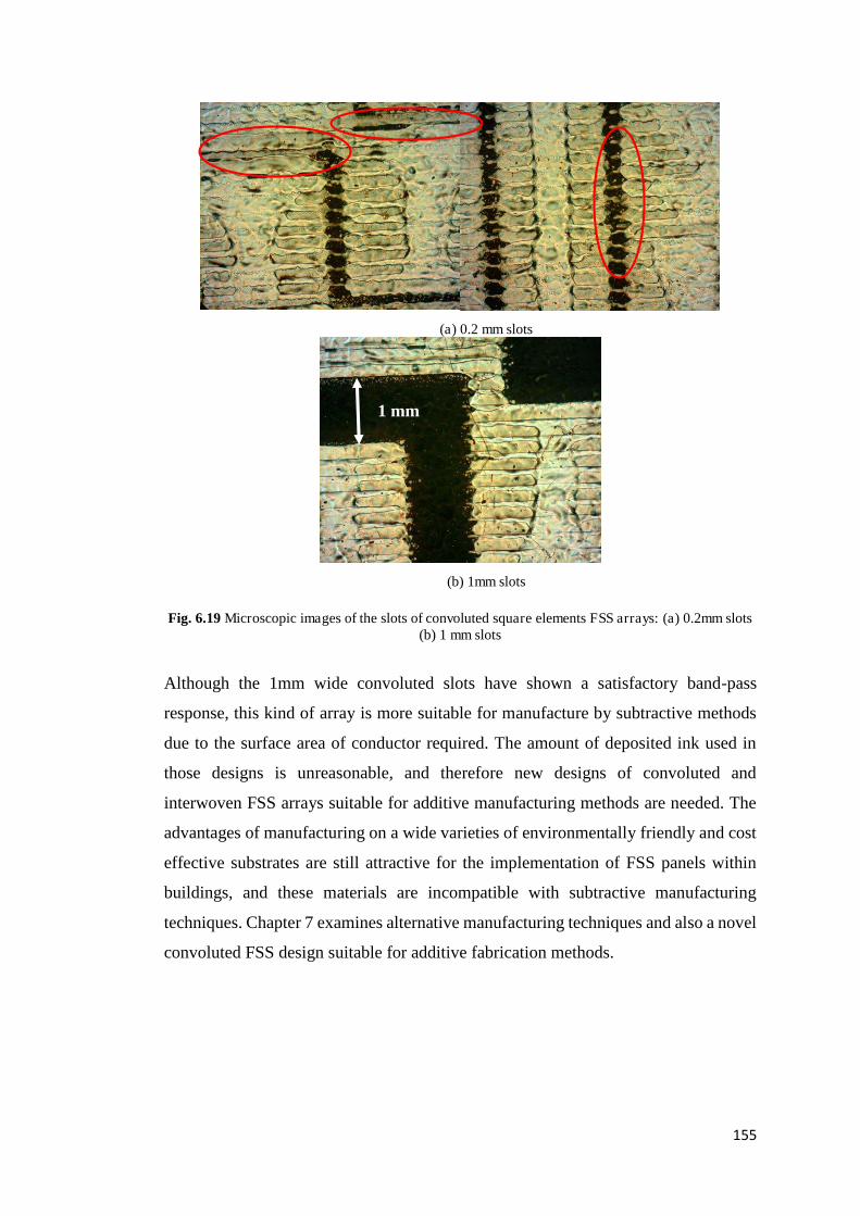
155
(a) 0.2 mm slots
(b) 1mm slots
Fig. 6.19 Microscopic images of the slots of convoluted square elements FSS arrays: (a) 0.2mm slots (b) 1 mm slots
Although the 1mm wide convoluted slots have shown a satisfactory band-pass
response, this kind of array is more suitable for manufacture by subtractive methods
due to the surface area of conductor required. The amount of deposited ink used in
those designs is unreasonable, and therefore new designs of convoluted and
interwoven FSS arrays suitable for additive manufacturing methods are needed. The
advantages of manufacturing on a wide varieties of environmentally friendly and cost
effective substrates are still attractive for the implementation of FSS panels within
buildings, and these materials are incompatible with subtractive manufacturing
techniques. Chapter 7 examines alternative manufacturing techniques and also a novel
convoluted FSS design suitable for additive fabrication methods.
1 mm

156
6.7 Conclusion
This chapter considered the manufacturing process of the convoluted square FSS
arrays intended for use in in-building environments with an acceptable level of
performance. Novel convoluted square elements were made by chemical etching and
their performance was compared with previously reported convoluted designs. The
degree of convolution complexity was chosen to provide good angular stability, and
high figures of merit similar to those reported in [9], while taking into consideration
the limitations in the printing process observed for the simple dipole and square loop
arrays.
The arrays were inkjet printed using SunTronic silver nanoparticle ink on PEL
substrates, and it was found that the benchmark isolation level of 20 dB was not
achieved by the semi-convoluted square loop (Maltese cross) and the convoluted
square element arrays. This was a result of discontinuities especially in the case of the
diagonal printed lines and also of non-uniformity in the vertical lines. It was noticed
that the vertical line point to point resistance was higher than for the horizontal lines
by 3 – 5Ω. Different printing techniques were adopted including altered line widths,
ink drop spacing, and multiple numbers of ink layers, in order to improve the
conductivity of the printed elements and thus the reflectivity of the FSS panels.
However, it was found that the benchmark isolation level of 20 dB was not yet
satisfied. Droplet interaction influenced by the rapid evaporation of the solvent was
the main cause of the poor line definitions, and hence the poor isolation level.
In addition, a second silver Nanoparticle ink, Silverjet, was used to print firstly simple
square loop elements. Several microscopic images of the elements were taken, and it
was found that the elements had better line definitions compared with their
counterparts that were printed with the SunTronic silver ink. The Silverjet ink consists
of greater silver dispersion, and is also more viscous compared to the SunTronic silver
ink leading to more uniform vertical lines. As a consequence, it was found that the
square elements had lower dc resistances than their equivalents printed with
SunTronic ink by about 14 and 10 Ω in the case of the 0.2 mm vertical and horizontal
lines.

157
Furthermore, although it was noticed that the average element dc resistances of the
Silverjet convoluted square elements were much lower than their SunTronic
counterparts, it was still necessary to increase the line width of the convoluted square
elements to 1 mm to achieve the benchmark isolation level of 20 dB. This was due to
the large amount of errors in the printed elements with tracks thinner than 1mm.
In this chapter, the fabrication of slots of elements arrays was considered for the first
time with two different slot widths. However, it is believed that the amount of
deposited ink is unrealistic for producing cost effective FSS panels. Therefore, a better
engineered slot and interwoven designs are needed in order to produce economical
FSS arrays, due to their great importance in operating in the wavelengths used by most
wireless technologies and mobile communications. Chapter 7 introduces a slot FSS
design that is inkjet print friendly while blocking mobile communication bands and
allowing transmission in the emergency European TETRA band.

158
References
[1] S. M. A. Hamdy and E. A. Parker, “Influence of lattice geometry on transmission of electromagnetic waves through arrays of crossed dipoles,” IEE Proc. H Microwaves, Opt. Antennas, vol. 129, no. 1, p. 7, 1982.
[2] R. Cahill and E. A. Parker, “Concentric Ring and Jerusalem Cross Arrays as Frequency Selective Surfaces for a 45° Incidence Diplexer,” Electron. Lett., vol. 18, no. 8, pp. 313–314, 1982.
[3] R. J. Langley and E. A. Parker, “Equivalent circuit model for arrays of square loops,” Electron. Lett., vol. 18, no. 7, p. 294, 1982.
[4] L. Li, Q. Chen, Q. Yuan, K. Sawaya, T. Maruyama, T. Furuno, and S. Uebayashi, “Frequency Selective Reflectarray Using Crossed-Dipole Elements With Square Loops for Wireless Communication Applications,” IEEE Trans. Antennas Propag., vol. 59, no. 1, pp. 89–99, Jan. 2011.
[5] E. A. Parker and R. J. Langley, “Double-square frequency-selective surfaces and their equivalent circuit,” Electron. Lett., vol. 19, no. 17, pp. 675–677, 1983.
[6] E. A. Parker and A. N. A. El Sheikh, “Convoluted dipole array elements,” Electron. Lett., vol. 27, no. 4, p. 322, 1991.
[7] E. A. Parker and S. M. A. Hamdy, “Rings as elements for frequency selective surfaces,” Electron. Lett., vol. 17, no. 17, p. 612, 1981.
[8] E. A. Parker, A. N. A. El sheikh, and A. C. de C. Lima, “Convoluted frequency-selective array elements derived from linear and crossed dipoles,” IEE Proc. H Microwaves, Antennas Propag., vol. 140, no. 5, p. 378, 1993.
[9] E. A. Parker and A. N. A. El sheikh, “Convoluted array elements and reduced size unit cells for frequency-selective surfaces,” IEE Proc. H Microwaves, Antennas Propag., vol. 138, no. 1, p. 19, 1991.
[10] B. Sanz-Izquierdo, E. A. Parker, J. B. Robertson, J. C. Batchelor, M. J. Neve, and A. G. Williamson, “Interwoven loops for electromagnetic architecture of buildings,” in 2010 IEEE Antennas and Propagation Society International Symposium, 2010, pp. 1–4.
[11] B. A. Munk, Frequency Selective Surfaces: Theory and Design. John Wiley & Sons, 2000.
[12] T. K. Wu, Frequency selective surface and grid array. J. Wiley, 1995.
[13] E. Arnaud, A. Kanso, T. Monediere, D. Passerieux, M. Thevenot, E. Beaudrouet, C. Dossou-yovo, and R. Noguera, “Inkjet printing of frequency selective surfaces on EBG antenna radome,” in 2012 6th European Conference on Antennas and Propagation (EUCAP), 2012, pp. 2693–2696.
[14] J. C. Batchelor, E. A. Parker, J. A. Miller, V. Sanchez-Romaguera, and S. G. Yeates, “Inkjet printing of frequency selective surfaces,” Electron. Lett., vol. 45, no. 1, p. 7, 2009.
[15] V. Sanchez-Romaguera, S. Wünscher, B. Turki, D. Oyeka, R. Abbel, B. Silvia, T. Daniel J., J. C. Batchelor, E. A. Parker, U. S. Schubert, and S. G. Yeates, “Inkjet printed paper based Frequency Selective Surfaces and on-skin RFID tags; the interrelation between silver nanoparticle ink, paper substrate and low

159
temperature sintering technique selection,” J. Mater. Chem. C, vol. 3, no. 9, pp. 2132–2140, 2015.
[16] R. D. Seager, J. Bowman, R. Philpott, a. Chauraya, M. Broughton, and N. Nimkulrat, “Fabric based frequency selective surfaces using weaving and screen printing,” Electron. Lett., vol. 49, no. 13, pp. 1507–1509, 2013.
[17] B. M. Turki, E. A. Parker, S. Wünscher, U. S. Schubert, R. Saunders, V. Sanchez-romaguera, M. A. Ziai, S. G. Yeates, and J. C. Batchelor, “Significant Factors in the Inkjet Manufacture of Frequency Selective Surfaces.” Submitted on June to IEEE Transactions on Components, packaging and Manufacturing Technology.
[18] B. M. Turki, E. A. Parker, J. C. Batchelor, M. A. Ziai, S. Wünscher, S. G. Yeates, and U. S. Schubert, “Inkjet Fabrication of Frame Dipole FSS,” in 2014 Loughborough Antennas & Propagation Conference (LAPC), 2014, pp. 347–349.
[19] B. M. Turki, E. A. Parker, M. A. Ziai, J. C. Batchelor, V. Sanchez-Romaguera, and S. G. Yeates, “Study of printing errors in digitally fabricated FSS,” in 2013 Loughborough Antennas & Propagation Conference (LAPC), 2013, pp. 429–432.
[20] B. M. Turki, E. A. Parker, M. A. Ziai, J. C. Batchelor, V. Sanchez-Romaguera, and S. G. Yeates, “Study of clusters of defects in low-cost digitally fabricated frequency selective surfaces,” in The 8th European Conference on Antennas and Propagation (EuCAP 2014), 2014, pp. 779–801.
[21] B. M. Turki, E. A. Parker, J. C. Batchelor, M. A. Ziai, S. G. Yeates, and V. Sanchez-Romaguera, “Influence of defective elements on performance of frequency selective surfaces,” Electron. Lett., vol. 49, no. 17, pp. 1054–1055, Aug. 2013.
[22] “PM000040 Rev. 05, DMP-2800 Series - DMP2800GuideVersion2.0.pdf.” [Online]. Available: http://www.lilliu.co.uk/resources/DMP/DMP2800GuideVersion2.0.pdf. [Accessed: 22-Aug-2015].
[23] C.-T. Chen and K.-Z. Tu, “Morphologies of conductive looped liquid lines inkjet-printed on substrate surfaces,” J. Micromechanics Microengineering, vol. 22, no. 5, p. 055001, 2012.
[24] E. A. Parker, “the Gentleman ’ S Guide To Frequency Selective Surfaces,” 17th Q.M.W. Antenna Symp., no. April, pp. 1–18, 1991.
[25] B. Sanz-Izquierdo, E. A. Parker, J.-B. Robertson, and J. C. Batchelor, “Singly and Dual Polarized Convoluted Frequency Selective Structures,” IEEE Trans. Antennas Propag., vol. 58, no. 3, pp. 690–696, Mar. 2010.
[26] “Silver nanoparticle ink <150 nm particle size (DLS), 20 wt. % (dispersion in organic solvents) | Sigma-Aldrich.” [Online]. Availableμ http://www.sigmaaldrich.com/catalog/product/aldrich/719048?lang=en®ion=GB. [Accessed: 22-Aug-2015].
[27] “Information Sheet for PEL Nano P60.pdf.” [Online]. Availableμ http://www.printedelectronics.co.uk/Information Sheet for PEL Nano P60.pdf. [Accessed: 22-Aug-2015].

160
[28] T. H. J. van鳥Osch, J. Perelaer, a. W. M. de鳥Laat, and U. S. Schubert, “Inkjet Printing of Narrow Conductive Tracks on Untreated Polymeric Substrates,” Adv. Mater., vol. 20, no. 2, pp. 343–345, 2008.
[29] B. J. Kang and J. H. Oh, “Geometrical characterization of inkjet-printed conductive lines of nanosilver suspensions on a polymer substrate,” Thin Solid Films, vol. 518, no. 10, pp. 2890–2896, 2010.
[30] A. M. J. van den Berg, A. W. M. de Laat, P. J. Smith, J. Perelaer, and U. S. Schubert, “Geometric control of inkjet printed features using a gelating polymer,” J. Mater. Chem., vol. 17, no. 7, p. 677, 2007.
[31] “Silver, dispersion nanoparticle, 30-35 wt. % in triethylene glycol monomethyl ether, spec. resistivity 11 たっ-cm, for printing on plastic films | Sigma-Aldrich.” [Online]. Available: http://www.sigmaaldrich.com/catalog/product/aldrich/736465?lang=en®ion=GB. [Accessed: 02-Oct-2015].

161
CHAPTER 7: FSS MANUFACTURE BY
ELECTROLESS COPPER PLATING ON AN
INKJET PRINTED CATALYST
7.1 Introduction
Screens of frequency selective surfaces have attracted attention owing to their
expected ability to offer improvements in the quality of radio communications within
buildings by reducing the signal-to-interference ratio from other devices in adjacent
floors, rooms, or buildings [1]–[6]. The use of these selective screens has been shown
to improve the signal to interference ratio, by as much as 15 dB for indoor
environments which can reduce the outage probability by a factor of 20 [7].
In order to make FSS screens cost effectively when applied in real built environments,
there are considerations to take into account such as production in a large scale,
efficient use of resource, use of flexible substrates and easy installation and
maintenance. With that aim, trials have demonstrated promising performance and cost
savings using FSS manufactured by additive fabrication technologies such as inkjet
printing with silver inks. FSS screens have been printed on various substrates such as
glass, textile, polyethylenenapthenate (PEN), and on paper substrates, and show
electromagnetic performance similar to those of chemically etched equivalents [8]–
[11].

162
However, it is thought the use of inkjet printing technology is more suitable when
producing patch elements of simple geometry and small size, for instance linear
dipoles and square loop elements. As the complexity and the resolution of the designs
increases, it becomes more challenging to obtain inkjet elements with low electrical
resistance due to limitations in the printing process. Examples of more complex
elements are the interwoven designs and slot type FSS screens described in Chapter 6.
Therefore as an alternative to direct deposition of conducting ink, inkjet printing of a
catalyst on PET for electroless copper plating fabrication method was considered. This
process was developed and provided by CIT Technology (Cambridge, UK), formally
owned by Carclo plc Group (West Yorkshire, UK) using electroless copper plating
deposition technology [12][13]. The electroless copper plating fabrication technique
has been used in manufacturing RFID tags, PCBs, and printed antennas, and was
considered a practical alternative to inkjet printing in the production of highly
convoluted slots of elements, and interwoven FSS arrays over a large area. The
fabrication process involves the inkjet patterning of FSS elements using a palladium
chloride catalyst solution on the supporting PET substrate, followed by immersing the
printed arrays in an electroless plating solution to deposit copper onto the printed
patterns [14]–[18]. As an additive fabrication technology, it provides the mask free
benefits gained with inkjet printing using conductive nanoparticle inks, but it is also
able to provide bulk metal elements with better performance closer to bulk metal
conductivities at low temperatures (30 – 50 °C) [17], with no sintering stage which
slows the process and causes thermal stress to substrate and also eliminates the issue
of nozzle clogging [14]. As an electroless bath is required, the CIT method is not
suitable for porous substrates.
This chapter compares the performance of the skewed lattice dipole elements, square
loop, and convoluted square FSS screens that were inkjet printed using silver
nanoparticle inks, and by the conventional chemical etching methods described in
Chapters 5 and 6, and with their equivalent designs manufactured by the CIT
electrolysis process.
Finally, a novel densely convoluted cross dipole element FSS array is discussed. This
design is considered to be suitable for additive means of fabrication and its
performance is compared with the interwoven FSS arrays reported in [19].

163
7.2 Skewed lattice dipole FSS arrays
The design under consideration for the fabrication process comparison was an array
of linear dipole patches arranged in a skewed lattice geometry, and identical to the
described in Section 4.2.1 and in [20], [21]. The arrays were manufactured by CIT
using the electroless copper plating fabrication method on PET substrates of thickness
(t) 0.1 mm and relative permittivity 鉛嘆 簡 ぬぬ. A finished sample is shown in Fig. 7.1.
The dipole arrays have the same unit cell dimensions and physical size of the
chemically etched and inkjet printed arrays presented in Chapters 4 and 5,
respectively, with periodicity (P = 10.4 mm) and length (L = 9.4).
Fig. 7. 1 Skewed lattice dipole FSS manufactured by electroless copper plating technique
The measured transmission response of the arrays were compared with their
chemically etched and single layer inkjet printed counterparts as illustrated in Fig. 7.2.

164
Fig. 7. 2 Measured transmission responses of skewed lattice dipole FSS screens
Along with the chemically etched and inkjet printed FSS screens, the electroless
copper coated FSS screen achieved an isolation level deeper than the benchmark of
20 dB [20], and had a null depth of about 30 dB. The resonant frequency was about
13.4 GHz compared with 14.4 and 12.6 for the chemically etched and inkjet printed
screens, respectively. The difference is believed to be mainly due to the difference in
the substrate thicknesses as was described in Fig. 5.9 in Section 5.3.1. Fig. 7.3 shows
the CST model results of the 3 FSS screens with their different parameters and good
agreement with the measured results can be observed. In addition, the electrolysis
copper coated dipoles had dc resistance values lower than 0.1 Ω compared to 4.3 Ω in
the case of the single layer inkjet printed dipole elements, and hence the deeper null
depth.
Furthermore, it was observed that about 10 dipole elements in the electrolysis sample
were narrower than expected and when examined under the microscope it was found
that those elements were only half of the required width of 0.4 mm. Therefore, 20
dipole elements were measured at random locations and it was found that the average
width was about 0.4 mm + / - 4 %. Similarly, the length of the selected 20 dipoles was
found to have an average length of 9.376 mm, about +/- 0.25 % than the intended
length.
The simulated transmission responses of the three arrays suggest that all screens
should achieve null depths deeper than the benchmark isolation level of -20 dB, with
null depths of -34 dB for the copper etched and electroless plated arrays. The simulated
-40
-35
-30
-25
-20
-15
-10
-5
0
10 11 12 13 14 15 16 17 18 19 20
S 21(d
B)
Frequency (GHz)
Electroless copper plated
Chemically etched
Inkjet printed

165
S21 of the inkjet printed arrays was about -29 dB. The difference between the
measured and simulated null depths of the inkjet printed arrays was due to the
variability in the resistance of each dipole element, whereas it is the same for all
dipoles in the modelled scenario. Furthermore, the simulated resonant frequencies of
the arrays were about 14.4, 13.5, and 12.5 GHz for the modelled chemically etched,
copper plated, and inkjet print arrays, respectively. Table. 7.1 summarises the
measured and simulated transmission responses of the skewed lattice dipole FSS
screen fabricated with electrolysis copper plating, inkjet printing and chemical
etching.
Fig. 7.3 Simulated transmission responses of the three skewed lattice dipole FSS screens:
(i) Electrolysis copper plated PET substrate 香追 簡 ぬぬ and t=0.1mm (ii) Chemically etched copper clad polyester substrate 香追 簡 ぬの and t=0.045mm (iii) Inkjet printed PEL substrate 香追 簡 ぬの and t=0.2 mm, conductor conductivity 1% bulk silver
TABLE. 7.1 SUMMARY OF THE SIMULATED (S) AND MEASURED (M) TRANSMISSION RESPONSES OF THE THREE FSS SCREENS
Fabrication
Method
F(S)
(GHz)
F(M)
(GHz)
S21 (S)
(dB)
S21 (M)
(dB)
Electrolysis
copper plating
13.5
13.4
-34
-30
Inkjet printing 12.5 12.6 -29 -25
Chemical etching 14.4 14.4 -34 -35
-40
-35
-30
-25
-20
-15
-10
-5
0
10 11 12 13 14 15 16 17 18 19 20
S 21(d
B)
Frequency (GHz)
Electroless copperplated
Chemically etched
Ink printed

166
7.3 Convoluted square element FSS arrays
The convoluted square patches and slots elements of FSS arrays described in Sections
6.2 and 6.6 were also fabricated using the electroless copper plating technology in
order to compare their performances with the copper etched and single layer inkjet
printed arrays. Fig. 7.4 shows the slot and patch versions of the convoluted square
elements FSS screens produced on PET.
(a) patch elements
(b) Slot elements
Fig. 7.4 Electroless copper plated convoluted square elements: (a) patches and (b) slots of elements FSS screens
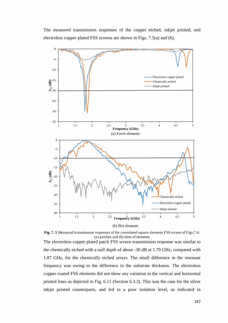
167
The measured transmission responses of the copper etched, inkjet printed, and
electroless copper plated FSS screens are shown in Figs. 7.5(a) and (b).
(a) Patch elements
(b) Slot elements
Fig. 7. 5 Measured transmission responses of the convoluted square elements FSS screen of Figs.7.4: (a) patches and (b) slots of elements
The electroless copper plated patch FSS screen transmission response was similar to
the chemically etched with a null depth of about -30 dB at 1.79 GHz, compared with
1.87 GHz, for the chemically etched arrays. The small difference in the resonant
frequency was owing to the difference in the substrate thickness. The electroless
copper coated FSS elements did not show any variation in the vertical and horizontal
printed lines as depicted in Fig. 6.11 (Section 6.3.3). This was the case for the silver
inkjet printed counterparts, and led to a poor isolation level, as indicated in
-35
-30
-25
-20
-15
-10
-5
0
1 1.5 2 2.5 3 3.5 4 4.5 5
S 21(d
B)
Frequency (GHz)
Electroless copper plated
Chemically etched
Inkjet printed
-40
-35
-30
-25
-20
-15
-10
-5
0
1 1.5 2 2.5 3 3.5 4 4.5 5
S 21(d
B)
Frequency (GHz)
Chemically etched
Electroless copper plated
Inkjet printed

168
Fig. 7.5 (a). Furthermore, the electroless plated slot version of the convoluted square
elements FSS panel was also similar to the chemically etched FSS screen in
performance, with S21 transmission above -10 dB for a frequency range of
1.1 – 2.4 GHz with a peak at about 1.74 GHz. This compared to 1.2 – 2.5 GHz range
with a peak at 1.8 GHz, and an insertion loss of approximately 1 dB, for the chemically
etched design as illustrated in Fig. 7.5 (b). The inkjet printed FSS screen suffered from
severe defects as a result of the ink droplet spreading which filled the slots, as was
illustrated in Fig. 6.19 (a) (Section 6.6) and did not function. Fig.7.6 shows the
simulated transmission responses of both patches and slots of convoluted square
element FSS screens.
(a) Patch elements
(b) Slot elements
Fig. 7.6 Simulated transmission responses of the convoluted square elements FSS screen of Figs. 7.4
-40
-35
-30
-25
-20
-15
-10
-5
0
1 1.5 2 2.5 3 3.5 4 4.5 5
S 21 (d
B)
Frequency (GHz)
Electroless copper plated
Chemically etched
Inkjet printed- 1% bulk silver conductivity
-40
-35
-30
-25
-20
-15
-10
-5
0
1 1.5 2 2.5 3 3.5 4 4.5 5
S 21(
dB)
Frequency (GHz)
Electroless copper plated
Chemically etched
Inkjet printed

169
The simulated results show similar trends to measurement especially in the case of the
chemically etched and copper plated FSS screens, and the performance of the inkjet
printed arrays when they are defect free with null depth of -18 dB.
7.4 Interwoven square loop slots FSS panel
In this section, more complicated FSS arrays with resolution too fine for inkjet printing
with silver nano particle inks such as the interwoven FSS arrays in [19] are considered.
The FSS screen was designed with the same parameters as described in [19], with unit
cell periodicity (P = 20 mm), length (l = 19 mm), conductor width (w = 0.22 mm), and
stub width (c =1.12 mm), as shown in Fig. 7.7. The FSS screen was designed to
provide a passband at the frequency range of about 0.2 – 1.2 GHz, e.g. allowing
transmission in the TETRA emergency band, and GSM900 band. For measurements
at such low frequency it was necessary to increase the size of the FSS filled aperture
from になど 抜 ぬどど mm2 to な 抜 な m2 to mitigate against issues such as signal scattering
[22]. As the electroless process is a roll to roll fabrication method, each FSS screen
had a standard width of about 33 cm, and in order to cover the aperture, four FSS were
joined together, as illustrated in Fig. 7.8. Log-periodic antennas with bandwidth
0.2 – 2 GHz were mounted 2 m before and behind the FSS screen. It was also necessary
to place absorbers on the floor to mitigate signal reflections due to the ground.
Fig. 7.7 Interwoven square loop patch unit cell [19]
C
P

170
The measured transmission response of the interwoven square loop slot FSS panel
fabricated using the electroless copper plating method was similar to the results
reported in [19] for an equivalent copper etched design. The measured -10 dB
transmission response width was from 240 – 1100 MHz with a peak at about 540 MHz,
and a higher order peak at 1950 MHz, as illustrated in Fig. 7.9. These results indicate
that the electroless method could be used for FSS production on a large scale.
Fig. 7.8 Measurement setup
Fig. 7.9 Measured transmission response of the interwoven square loop FSS panel produced by roll
to roll electrolysis method
In addition, there is a need for optimising FSS designs with the minimum amount of
conductor to be more suitable for additive fabrication technologies, such as by using
frame dipoles [11], [23], particularly at long wavelength bands where the elements are
large.
-20
-18
-16
-14
-12
-10
-8
-6
-4
-2
0
0.2 0.6 1 1.4 1.8
S 21(d
B)
Frequency (GHz)
1 m
1 m
2 m
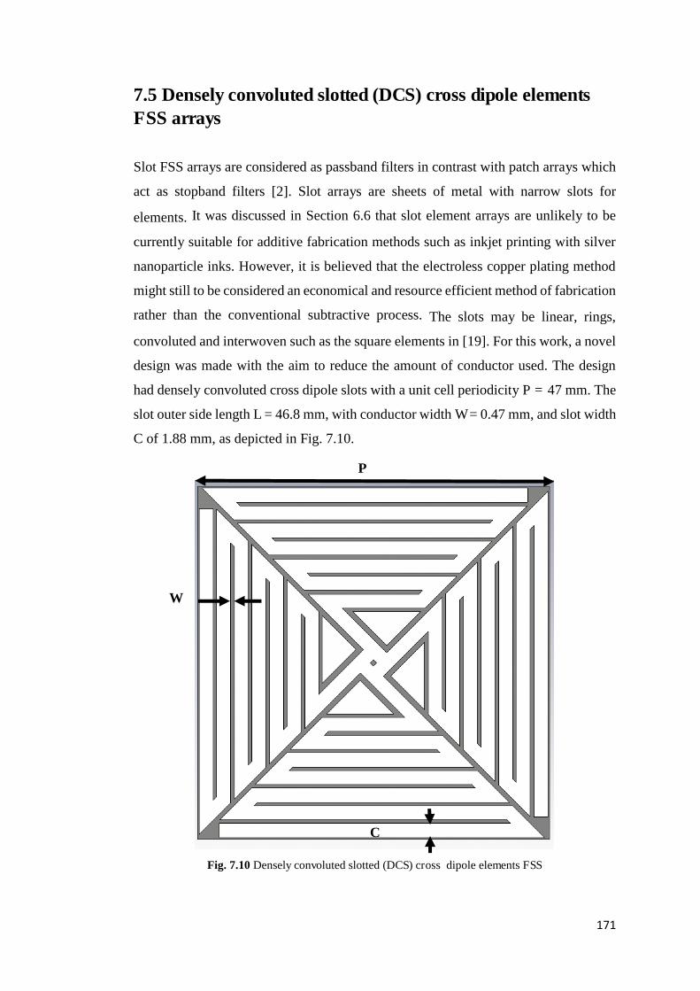
171
7.5 Densely convoluted slotted (DCS) cross dipole elements FSS arrays
Slot FSS arrays are considered as passband filters in contrast with patch arrays which
act as stopband filters [2]. Slot arrays are sheets of metal with narrow slots for
elements. It was discussed in Section 6.6 that slot element arrays are unlikely to be
currently suitable for additive fabrication methods such as inkjet printing with silver
nanoparticle inks. However, it is believed that the electroless copper plating method
might still to be considered an economical and resource efficient method of fabrication
rather than the conventional subtractive process. The slots may be linear, rings,
convoluted and interwoven such as the square elements in [19]. For this work, a novel
design was made with the aim to reduce the amount of conductor used. The design
had densely convoluted cross dipole slots with a unit cell periodicity P = 47 mm. The
slot outer side length L = 46.8 mm, with conductor width W = 0.47 mm, and slot width
C of 1.88 mm, as depicted in Fig. 7.10.
Fig. 7.10 Densely convoluted slotted (DCS) cross dipole elements FSS
P
W
C

172
The physical size of the FSS screen was 1 m2 and it was fabricated using the
conventional chemical etching method on copper clad polyester substrate, with
substrate relative permittivity香追 噺 ぬの, substrate thickness of 0.045 mm and loss
tangent 購 噺 どどに. However, due to the area limitation of the etching facilities used,
the complete FSS screen was comprised of approximately 20 sheets of になど 抜 ぬどど mm2 panels. The same measurement arrangement as shown in Fig. 7.8 was
used. Fig. 7.11 shows the measured transmission response with -10 dB bandwidth
from 240 MHz to 730 MHz. The transmission peaks at around 500 MHz with an
insertion loss of about 1 dB, and the figure of merit of element compression そ1/P at
500 MHz is about 13. Furthermore, the narrow band transition simulated at 1.34 GHz
was not observed in measurements. Compared with the interwoven convoluted square
slot FSS elements shown in Fig. 7.7, the densely convoluted cross slotted dipole FSS
has a narrower -10 dB bandwidth. The ratio of the two was about 0.57, and fractional
bandwidth ratio of 0.77. The fractional bandwidth of the DCS cross dipole arrays was
about 1 .This could block GSM900 mobile frequency bands according to the measured
results from approximately 800 MHz to 1.5 GHz unlike the interwoven FSS design as
shown in Figs. 7.9 and 7.11.
Fig. 7.11 Measured transmission response of the densely convoluted cross dipole elements FSS panel
Owing to the aperture shape in the measurement setup, it was difficult at this stage to
investigate the influence of oblique angles of incidence, however, simulation results
suggest acceptable angular stability as shown in Fig. 7.12.
-20
-18
-16
-14
-12
-10
-8
-6
-4
-2
0
0.2 0.4 0.6 0.8 1 1.2 1.4 1.6 1.8 2
S 21(d
B)
Frequency (GHz)
Measured -TM
Measured -TE
Simulated
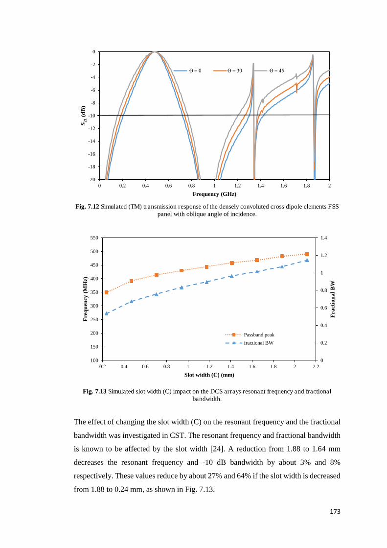
173
Fig. 7.12 Simulated (TM) transmission response of the densely convoluted cross dipole elements FSS
panel with oblique angle of incidence.
Fig. 7.13 Simulated slot width (C) impact on the DCS arrays resonant frequency and fractional
bandwidth.
The effect of changing the slot width (C) on the resonant frequency and the fractional
bandwidth was investigated in CST. The resonant frequency and fractional bandwidth
is known to be affected by the slot width [24]. A reduction from 1.88 to 1.64 mm
decreases the resonant frequency and -10 dB bandwidth by about 3% and 8%
respectively. These values reduce by about 27% and 64% if the slot width is decreased
from 1.88 to 0.24 mm, as shown in Fig. 7.13.
-20
-18
-16
-14
-12
-10
-8
-6
-4
-2
0
0 0.2 0.4 0.6 0.8 1 1.2 1.4 1.6 1.8 2
S 21(d
B)
Frequency (GHz)
事 = 0 事 = 30 事 = 45
0
0.2
0.4
0.6
0.8
1
1.2
1.4
100
150
200
250
300
350
400
450
500
550
0.2 0.4 0.6 0.8 1 1.2 1.4 1.6 1.8 2 2.2
Fra
ctio
nal B
W
Fre
quen
cy (
MH
z)
Slot width (C) (mm)
Passband peak
fractional BW

174
The densely convoluted cross dipole FSS of Fig. 7.10 was also fabricated with reduced
unit cell dimensions of periodicity P = 19.75 mm, length L = 19.47 mm, conductor
width w = 0.56 mm, and slot width C = 0.84 mm. The aim was to fabricate frequency
selective panels intended for buildings that require more data security by allowing
mobile communication bands between 800 MHz and 2.3 GHz to propagate while
blocking WiFi frequencies at 2.4 GHz. It was found that the insertion loss was about
-14 dB at 2.4 GHz, which would be sufficient to increase the quality of wireless
communication within buildings and the data integrity within buildings, as was
pointed out in [7]. Fig. 7.14 shows the measured and simulated transmission responses
of the modified densely convoluted cross dipole FSS screen. Measurements gave
a -10 dB pass band from about 880 MHz to 2.2 GHz, agreeing with simulations from
770 MHz to 2.3 GHz, and with a very narrow peak at about 4.4 GHz. The pass band
has a peak at around 1.6 GHz with an insertion loss of about 1 dB in the measured S21.
Fig. 7.14 Measured transmission responses of the densely convoluted slotted cross dipole elements
FSS panel with periodicity (P =19.75 mm)
The effect of oblique angles of incidence was also considered, where the FSS
performance was investigated at 30° and 45°, as illustrated in Fig. 7.15. The -10 dB
passband bandwidth increases as the oblique angle of incidence increases from normal
incidence by, about 12%, and 18% respectively for 30° and 45° incidence. Fig. 7.16
shows the simulated transmission responses at the same angles.
-20
-18
-16
-14
-12
-10
-8
-6
-4
-2
0
0.8 1.3 1.8 2.3 2.8 3.3 3.8 4.3 4.8
S 21(d
B)
Frequency (GHz)
TE-0
TM-0
Simulated

175
Fig. 7.15 Measured (TM) transmission responses of the densely convoluted cross dipole elements FSS
panel (P =19.75 mm) with oblique angels of incidence
Fig. 7.16 Simulated (TM) transmission responses of the densely convoluted cross dipole elements FSS
panel (P =19.75 mm) with oblique angels of incidence
Unfortunately, it was not possible to fabricate these arrays with the electroless copper
plating technology at the time of writing, however, there are plans to fabricate using
additive technology in the future owing to the design simplicity and conductor savings
compared with the interwoven FSS arrays. The aim will be to install them into a real
building environment once fabricated and to expand the investigation.
-20
-18
-16
-14
-12
-10
-8
-6
-4
-2
0
0.8 1.3 1.8 2.3 2.8 3.3 3.8 4.3 4.8
S 21(d
B)
Frequency (GHz)
TE-0
TE-30
TE-45
-20
-18
-16
-14
-12
-10
-8
-6
-4
-2
0
0.8 1.3 1.8 2.3 2.8 3.3 3.8 4.3 4.8
S 21(d
B)
Frequency (GHz)
事 = 0事 = 30事 = 45

176
The densely convoluted cross dipole elements (P = 47 mm) in Fig. 7.10 had a saving
of about 76% in the amount of metal used compared with the interwoven square loop
FSS arrays shown in Fig. 7.7 (P = 20 mm). This was calculated over the 1m2 FSS
screen. The densely convoluted cross dipole elements had a total metal content of 12%
compared to the 49% calculated for the interwoven square loop slots FSS screen.
Such savings suggest that additive fabrication methods are more favourable than
subtractive fabrication methods such as the chemical etching in producing large scale
FSS panels especially when metal savings are considered in the FSS panels. Table. 7.2
summarises the figures of merit, fractional bandwidth, and metal content of the
interwoven square loop slots (Fig. 7.7), and DCS cross dipole (Fig. 7.10) FSS arrays.
TABLE. 7. 2 SUMMARY OF THE SIMULATED (S) AND MEASURED (M) TRANSMISSION RESPONSES OF THE INTERWOVEN AND DCS CROSS DIPOLES FSS SCREENS
FSS そ1/P Fractional BW Metal content
(%)
(A = 1 m2)
Interwoven square
loop slots
28 1.3 49
DCS cross dipoles 13 1 12

177
7.6 Conclusion
This chapter has demonstrated the manufacturing of frequency selective screens
intended for in-building applications on an industrial scale using roll to roll electroless
copper plating technology. Trial samples of various FSS designs have been
manufactured, beginning with simple dipole elements arranged in a skewed lattice
geometry. The performance of these arrays proved to provide satisfactory isolation
levels, and their performance was compared with their silver inkjet printed and
chemically etched counterparts. More complex elements such as convoluted squares
with line width of 0.2 mm, Fig. 7.4 (a), did not achieve the benchmark isolation level
of -20 dB when inkjet printed. However, the electroless copper plated counterpart
provided a null of about -30 dB similar to the chemically etched version, without the
need of increasing the line width to 1mm as was the case with the inkjet printed
convoluted square elements in Chapter 6. Furthermore, slot arrays were also
considered owing to their band pass capabilities; such as convoluted square element
slots in Fig. 7.4 (b), and the interwoven square loops in (Fig. 7.7) reported in [19].
Both screens provided a satisfactory -10 dB pass band from 1.2 – 2.5 GHz and
0.27 – 1.1 GHz for the convoluted square slots and the interwoven square loops
respectively, when they were produced by electroless copper plating method. Their
transmission responses were similar to their chemically etched counter parts,
containing no defects, as was reported in Section 6.6.
In addition, a new FSS design was developed to allow transmission in some selected
frequency bands such as the governmental emergency service band (TETRA), while
reflecting in the mobile bands. The densely convoluted cross dipole element FSS
provides transmission from 240 – 730 MHz, with a transmission peak at about 500
MHz, providing transmission in the TETRA emergency band while providing total
reflection in the frequency range 800 MHz to 1.3 GHz. The -10 dB pass band of the
new arrays is about 0.57 of the interwoven FSS in [19] which was not selective enough
in the frequency range 880 – 1100 MHz. The new FSS design is believed to be suitable
for additive fabrication methods due to the expected savings the deposited conducting
materials.

178
Simulation results showed good agreement with measurements, however, due to the
current measurement setup it was not possible to investigate the stability of the arrays
toward oblique angles of incidence, owing to space limitations in the measurement
chamber.
Special arrangements would be implemented when the arrays are manufactured using
roll to roll additive technology such as electroless copper plating and installed in one
of the offices in the school of Engineering at the University of Kent. On the contrary,
simulation results suggest that the arrays are stable toward oblique incidence up to 45°.
The reduction of the unit cell size by 50% allows the transmission in the mobile
communication frequency band from 880 MHz – 2.3 GHz while blocking radio
communications below the -10 dB level from 2.3 GHz to about 4.8 GHz providing
more secured indoor communications in the Wi-Fi bands.

179
References
[1] M. Philippakis, C. Martel, D. Kemp, S. Appleton, R. Pearson, and E. A. Parker, “Application of FSS Structures to Selectively Control the Propagation of signals into and out of buildings, Annex 3,” Ofcom ref AY4464, pp. 1–54, 2004.
[2] B. A. Munk, Frequency Selective Surfaces: Theory and Design. John Wiley & Sons, 2000.
[3] E. A. Parker, J. C. Batchelor, R. Chiang, A. G. Williamson, B. Sanz-Izquierdo, M. J. Neve, and K. W. Sowerby, “Frequency selectively screened office incorporating convoluted FSS window,” Electron. Lett., vol. 46, no. 5, p. 317, 2010.
[4] E. A. Parker and S. B. Savia, “Fields in an FSS screened enclosure,” IEE Proc. - Microwaves, Antennas Propag., vol. 151, no. 1, p. 77, 2004.
[5] B. Sanz-Izquierdo, E. A. Parker, J. B. Robertson, J. C. Batchelor, M. J. Neve, and A. G. Williamson, “Interwoven loops for electromagnetic architecture of buildings,” in 2010 IEEE Antennas and Propagation Society International Symposium, 2010, pp. 1–4.
[6] G. Sung, K. Sowerby, M. Neve, and A. Williamson, “A Frequency-Selective Wall for Interference Reduction in Wireless Indoor Environments,” IEEE Antennas Propag. Mag., vol. 48, no. 5, pp. 29–37, Oct. 2006.
[7] A. H. Wong, M. J. Neve, and K. W. Sowerby, “Performance analysis for indoor wireless systems employing directional antennas in the presence of external interference,” 2005 IEEE Antennas Propag. Soc. Int. Symp., vol. 1A, pp. 799–802, 2005.
[8] J. C. Batchelor, E. A. Parker, J. A. Miller, V. Sanchez-Romaguera, and S. G. Yeates, “Inkjet printing of frequency selective surfaces,” Electron. Lett., vol. 45, no. 1, p. 7, 2009.
[9] E. Arnaud, A. Kanso, T. Monediere, D. Passerieux, M. Thevenot, E. Beaudrouet, C. Dossou-yovo, and R. Noguera, “Inkjet printing of frequency selective surfaces on EBG antenna radome,” in 2012 6th European Conference on Antennas and Propagation (EUCAP), 2012, pp. 2693–2696.
[10] V. Sanchez-Romaguera, S. Wünscher, B. Turki, D. Oyeka, R. Abbel, B. Silvia, T. Daniel J., J. C. Batchelor, E. A. Parker, U. S. Schubert, and S. G. Yeates, “Inkjet printed paper based Frequency Selective Surfaces and on-skin RFID tags; the interrelation between silver nanoparticle ink, paper substrate and low temperature sintering technique selection,” J. Mater. Chem. C, vol. 3, no. 9, pp. 2132–2140, 2015.
[11] B. M. Turki, E. A. Parker, S. Wünscher, U. S. Schubert, R. Saunders, V. Sanchez-romaguera, M. A. Ziai, S. G. Yeates, and J. C. Batchelor, “Significant Factors in the Inkjet Manufacture of Frequency Selective Surfaces.” Submitted on June to IEEE Transactions on Components, packaging and Manufacturing Technology.

180
[12] “Reps-Acts-2008.ashx.”Available: http://carclo.production.investis.com/investorcentre/~/media/Files/C/Carclo/pdfs/Reps-Acts-2008.ashx. [Accessed: 08-Oct-2015].
[13] “CIT Technology launches new website - Cambridge Network.” [Online]. Available: http://www.cambridgenetwork.co.uk/news/cit-technology-launches-new-website/. [Accessed: 08-Oct-2015].
[14] B. S. Cook, Y. Fang, S. Kim, T. Le, W. B. Goodwin, K. H. Sandhage, and M. M. Tentzeris, “Inkjet catalyst printing and electroless copper deposition for low-cost patterned microwave passive devices on paper,” Electron. Mater. Lett., vol. 9, no. 5, pp. 669–676, 2013.
[15] S. Kim, I. Bito, S. Jeong, and M. M. Tentzeris, “A Flexible Hybrid Printed RF Energy Harvester Utilizing Catalyst - based Copper Printing Technologies for Far-Field RF Energy Harvesting Applications,” IEEE International Microwave Symposium (IMS), vol. 339, pp. 0–3, 2015.
[16] N. V Mandich, A. E. Concepts, and E. Toro, “Fundamentals of Electroless Copper Bath Operation for Printed Circuit Boards,” no. January, pp. 33–36, 1993.
[17] A. J. Cobley, B. Abbas, and A. Hussain, “Improved Electroless Copper Coverage at Low Catalyst Concentrations and Reduced Plating Temperatures enabled by Low Frequency Ultrasound,” Int. J. Electrochem. Sci, vol. 9, pp. 7795–7804, 2014.
[18] S. Busato, A. Belloli, and P. Ermanni, “Inkjet printing of palladium catalyst patterns on polyimide film for electroless copper plating,” Sensors Actuators B Chem., vol. 123, no. 2, pp. 840–846, 2007.
[19] B. Sanz-Izquierdo, E. A. Parker, J.-B. Robertson, and J. C. Batchelor, “Singly and Dual Polarized Convoluted Frequency Selective Structures,” IEEE Trans. Antennas Propag., vol. 58, no. 3, pp. 690–696, Mar. 2010.
[20] B. M. Turki, E. A. Parker, J. C. Batchelor, M. A. Ziai, S. G. Yeates, and V. Sanchez-Romaguera, “Influence of defective elements on performance of frequency selective surfaces,” Electron. Lett., vol. 49, no. 17, pp. 1054–1055, Aug. 2013.
[21] S. M. A. Hamdy and E. A. Parker, “Influence of lattice geometry on transmission of electromagnetic waves through arrays of crossed dipoles,” IEE Proc. H Microwaves, Opt. Antennas, vol. 129, no. 1, p. 7, 1982.
[22] E. A. Parker, J.-B. Robertson, B. Sanz-Izquierdo, and J. C. Batchelor, “Minimal size FSS for long wavelength operation,” Electron. Lett., vol. 44, no. 6, p. 394, 2008.
[23] B. M. Turki, E. A. Parker, J. C. Batchelor, M. A. Ziai, S. Wünscher, S. G. Yeates, and U. S. Schubert, “Inkjet Fabrication of Frame Dipole FSS,” in 2014 Loughborough Antennas & Propagation Conference (LAPC), 2014, pp. 347–349.
[24] R. J. Langley and E. A. Parker, “Double-Square Frequency-Selective Surfaces and Their Equivalent Circuit,” Electron. Lett., vol. 19, no. 17, pp. 675–677, 1983.

181
CHAPTER 8: CONCLUSIONS AND FUTURE
WORK
This thesis has examined the manufacture by inkjet printing of
frequency selective panels intended for indoor applications. Various manufacturing
factors have been covered in order to achieve the most economical manufacturing such
as reducing the amount of deposited ink, and decreased sintering times. The research
also examined the printing of square loops and convoluted elements and the features
that need to be considered whilst printing complex FSS designs. Alternative methods
of additive manufacturing on an industrial scale have been considered such as the
creating FSS screens using the inkjet printing of catalyst on PET substrates for
electroless copper plating. This chapter provides a summary of conclusions raised
from the research and the recommended future work.

182
8.1 Conclusions
The adoption of frequency selective walls has been recommended as a means of
improving the quality and security of wireless communication channels. The use of
Wireless technologies continues to increase and interference suppression with
protected network access will be a primary concern in the forthcoming time of the
Internet of Things. The ability to selectively pass or block certain frequency bands is
of a great interest and Frequency selective surfaces could provide an appropriate
resolution according to the nature of the built environment. Chapter 2 has provided an
insight of the different types of FSS arrays and the important factors that should be
considered during the design of those arrays.
However, the implementation of those frequency selective panels needs to be cost
effective and suitable for different building constructions, e.g. curved walls, and glass
panels. Inkjet printing as an emerging additive technology is suited to the manufacture
of electromagnetic structures owing to its precise features of fabrications and fewer
manufacturing stages, in comparison to other subtractive manufacturing methods such
as wet chemical etching. Inkjet printing technology offers an on demand deposition of
conductor which ensures efficient usage of resources in contrast with chemical etching
which removes unwanted metal and leads to significant wastage, which would need
several stages to reclaim. Additionally, the use of cheap and environmentally
sustainable substrates is another advantage of additive manufacturing methods. For
instance the ability exists to print on porous substrates such as paper, textile, and wood
in addition to the various kinds of substrates that are used with subtractive
manufacturing means. Inkjet printing technology has been discussed in more detail in
Chapter 3 which includes different printing mechanisms and sintering techniques.
As one of the aims of this research was to produce low cost FSS screens in order to
make them practical for real life applications, imperfections would be expected during
the mass production of those arrays owing to variations in the conductivity of the
printed elements or the mishandling of the FSS printed screens. Chapter 4 examined
various situations where the imperfections were intentionally introduced in a random
manner, or in clusters, in the copper etched FSS arrays. The purpose was to understand
the amount of imperfections that could be accepted whilst attaining an adequate level

183
of isolation. A 20 dB level was chosen as the benchmark isolation limit for an
acceptable band stop performance, as it resembles to only a 1% signal transmission
though the structure. Chapter 4 concluded that in the case of the random distribution
of defects across the FSS board, a range of 15 – 20% of defects could be tolerated
whilst meeting the 20 dB benchmark isolation level. This was concluded according to
the investigations of the intentionally produced defects of 10, 20, 30, and 40% in the
form of absent or broken elements in a totally arbitrary manner on various FSS
elements such as dipole, square and ring loops elements. However in the case of strong
clusters of absent elements in the centre of the arrays, it seemed that clusters of 10%
of missing elements did not achieve the 20 dB level of isolation. Furthermore, the
effect of 20% clustering at the corners of the arrays was less deleterious where the
arrays null depths were deeper than -20 dB. This arises from illumination tapering in
both the measurements and simulations. Changes in the illumination profile across an
FSS integrated into a wall could be significant in a real building environment due to
multipath and varying incidence angles meaning the position of missing element
clusters may change in importance with time.
Chapter 5 demonstrated the inkjet printing of simple dipole element FSS screens. The
screens were printed with different ink drop spacings (15, 20 and 25 µm) in order to
achieve reasonable conductivity of elements and hence a stop band null deeper than
the defined 20 dB isolation level. This was carried out on 2 different substrates, PEL,
and transfer, paper. The printed elements were then treated with 3 different sintering
techniques in order to find the best FSS performance and to optimise the printing
process. It was found that the elements printed on transfer paper suffered from severe
levels of defects in the form of cracks when treated with plasma and photonic sintering
methods. Those defects were of significant quantities, for example, the FSS sintered
with intense pulse light (IPL) had 24 and 90% non-conductive elements in the case of
20 and 25 µm drop spacing. In addition, the elements which showed good line
continuity had high dc resistance of about 24 and 36 Ω, for the respective drop
spacings. This affected strongly the reflectivity of the FSS arrays and made them
unreliable. It was found that the cause of the cracks was due to softening and wrinkling
damage to the thermally sensitive transfer paper polymeric receiving layer (PVA).
The level of defects was higher in the case of multiple ink layer deposition as also
encountered in Chapter 3. However, FSS elements printed on PEL paper have shown

184
more crack robustness to the IPL and plasma sintering treatments, and hence sufficient
null depth for no defects and 0.8% non-conductive elements in the case of photonics
and plasma sintering, for the respective sintering techniques. This was owing to the
difference in the thermo-mechanical stability of the ink receiving layers between the
PEL and transfer paper.
An evaluation of transmission responses and resistance measurements was conducted
for several FSS arrays treated with thermal, plasma and IPL sintering. It was found
that the elements printed on PEL paper gave the best performance in terms of average
element conductivity about 2 – 5% of bulk silver conductivity and transmission null
depths (20 – 24 dB) for single layer ink deposition of line width 0.4 mm, as
summarised in Table 5.3. Thermal sintering of the elements printed with 15 µm drop
spacing at 150C for 30 minutes achieved the best line conductivity with no defects in
elements. These conductivity values are much higher than those reported in Table 3.1
(Chapter 3) which were obtained with only a single ink layer with very short sintering
times.
Furthermore, the introduction of frame dipole elements with edge line widths of
70 µm, showed good reflectivity of about 20 dB. These line widths are difficult to
achieve with conventional wet etching which has a minimum line width of about
0.15 mm. This was achieved with about 50% saving in the amount of deposited ink in
comparison to their solid equivalents. The multi-layer deposition feature of inkjet
printing also enabled the introduction of superimposed elements where a layer of
frame was deposited over a single complete layer of the filled dipole elements. This
improved the null depth of the arrays by about 7 dB in comparison with the single
layer solid elements, whilst achieving ink savings of 25% in contrast with double layer
solid dipoles. Chapter 5 provides a detailed examination of these achievements and
also discusses the imperfections that were noticed during the printing and sintering
processes.
Chapter 6 investigated the fabrication of more complex elements such as square loop,
Maltese cross, and convoluted element FSS arrays. Although, the convoluted square
elements were designed with moderate convolution complexity, it was found that these
elements suffered from severe deficiencies owing to the limitations in the printing

185
equipment. The deficiencies were mainly found in the vertical and diagonal lines,
which were not observed in the horizontally printed linear dipoles with the defects
being in the form of discontinuities or non-uniformity in the printed lines. It is believed
that the main factor leading to such faults was the mechanism of the printer which
affected the adjacent droplet interactions. Different trials were made with the aim of
improving the printed line continuity, such as different droplet separation, multiple ink
layers and different silver inks. The deposition of an extra ink layer improved the null
depth of single layer square loop elements from -18 to -26 dB. However, this was not
the case with the convoluted elements which only achieved an acceptable null depth
of -23 dB when the element width was increased from 0.2 to 1 mm. All of those trials
are discussed in depth in Chapter 6.
The manufacture of slotted FSS designs using additive technologies such as inkjet
printing of silver nanoparticle ink may not be practical owing to the large amount of
conductor that is required. However, the advantageous use of flexible and
environmentally friendly substrates is still of a great interest. Therefore, a novel
densely convoluted slotted cross dipole FSS screen has been introduced in Chapter 7,
which was designed to be suitable for additive manufacturing methods operating in
the frequency band 240 – 730 MHz. The FSS arrays had a total metal content of 12%
over an area of 1m2, which makes it a candidate for additive fabrication methods.
Improving the resolution and conductivity of the inkjet printed elements depends on
various factors that must be considered such as:
- Properties of the nanoparticle ink used: Ink properties play an important role
on the droplet spreading effects on the substrate, such as how viscous the ink
is, and the type of solvents included, which in turn would determine the
maximum treating temperature without leading to excessive solvent
evaporation, and thus undesirable cracks. Some of the issues experienced, are
shown in Figs.5.6 and 6.9.
- Printer settings: Such as print head temperature, distance from the substrate
and mechanical movement, contact angle, droplet frequency and the printer’s
software algorithm as well as the substrate platen temperature. All of these
need to be optimised in order to improve the quality of the printed elements,
see for example Fig.6.14 which shows the effect of substrate heating on

186
improving the element conductivity which is obtained at a certain temperature
before reducing again if overheated.
- Droplet spacing: As depicted in Fig.3.4 in Section 3.2.2, insufficient overlap
of droplets could lead to discontinuities. Choosing the optimum droplet
spacing could also depend on the element geometry, where for instance narrow
convoluted elements with track orientations not aligned with the print head
direction might suffer discontinuities due to too low droplet spreading.
- Number of deposited layers: Multiple ink layers are considered as a means of
improving the electrical conductivity and line definition of the printed lines, as
was described in Chapters 5 and 6. However in the case of highly convoluted
and dense elements, multiple layer deposition might lead to undesirable
element interconnections, where adjacent lines short circuit. The sintering
regime is also complicated by the deposition of multiple layers.
- Substrate and ink receiving layer: The substrate characteristics such as
porosity and surface tension, controls the spreading of ink droplets. In the case
of coated paper based substrates compared to ordinary paper, the properties of
the ink receiving layer plays an important part alongside the paper backing
substrate in the droplet spreading and also during the process time and
temperature, where excessive sintering could lead to damage in the substrate
and thus to the degraded printed elements as was reported in Section 5.2.2.
- Substrates should be properly cleaned in order to remove dust particles which
could cause voids in the deposited ink and discontinuity in the printed tracks.
Chapter 7 has also demonstrated an alternative additive fabrication method. The inkjet
printing of catalyst for electroless copper plating on a roll-to-roll scale has been
considered. A performance analysis of inkjet printed, and copper etched, dipoles, and
convoluted square loops, is presented in Chapters 5 and 6. Comparison of printed and
etched designs is also made to electroless copper platted FSS which achieved
satisfactory null depths, similar to the copper etched equivalents. This is owing to the
high element conductivity produced by the electroless fabrication which is closer to
the copper etched elements.

187
8.2 Future Work
This thesis has presented the digital fabrication of frequency selective screens using
inkjet printing technology. Further investigations are recommended in order to achieve
larger scale in both the fabrication process and the employment of the manufactured
FSS in real life. A list of recommended further investigations is given:
Understanding the impact of deficiencies in the frequency selective screens
when they are installed onto walls within a room to verify the results obtained
in this research. For instance evaluating the effect of non-uniform illumination
on the performance of the FSS.
Investigating other available sintering techniques such as laser sintering owing
to its selective sintering capabilities which do not affect the substrate.
The possibility of using printers to print single entire elements before
advancing to the next element. This is proposed to improve the printed line
resolution, where it ensures the deposition of the next droplet in a short time
to ensure desired droplet interactions.
There is a need for manufacturing the densely convoluted slotted cross dipole
FSS using an additive technology due to the metal volume savings. Once
manufactured, it is suggested to investigate the stability toward oblique angles
of incidence.
It was noticed in Chapter 7 that the densely convoluted slotted cross dipole
FSS arrays in their current design did not provide sufficient rejection levels at
frequencies higher than 1.5 GHz which might allow transmission in the
wireless communication bands of (DCCS 1800, DECT, UMTS and
Bluetooth). Further design modifications are recommended to increase the
rejection frequency band to include mobile communications between 1.5 – 2
GHz. The main aim of the densely convoluted slotted cross dipole FSS was to
demonstrate operation in the TETRA band with the least amount of conductor
usage possible.