Karnataka Semiconductor Policy - 2010€¦ · Karnataka Semiconductor Policy - 2010. ... ‘design...
20
Karnataka Semiconductor Policy - 2010
Transcript of Karnataka Semiconductor Policy - 2010€¦ · Karnataka Semiconductor Policy - 2010. ... ‘design...
Karnataka Semiconductor Policy - 2010

Sri Katta Subramanya Naidu Hon’ble Minister for IT & BT,
Information, Housing & BWSSB Govt. of Karnataka
Sri B.S. Yeddyurappa Hon’ble Chief Minister Govt. of Karnataka
“The Semiconductor industry is a key driver, enabler and indicator of technological progress for the emerging dynamic digital market ”
“The Semiconductor design edge that Karnataka State has would be leveraged to cut
digital corners globally ”
contents
Overview 03
Global Outlook 04
Indian Scenario 04
Government of India’s (Gol) Semiconductor Policy, 2007 05
Objectives 06
Need for a Karnataka Specific Semiconductor Policy 06
Key Activities to be Undertaken - Semiconductor Design 06
Key Activities to be Undertaken - Semiconductor Manufacturing 08
Key Activities to be Undertaken to Promote Green Energy 12
Focus on Manpower Development 13
Fiscal Incentives 14
Investment Promotion Subsidy 14
Exemption from Stamp Duty 14
Concessional Registration Charges 14
Waiver of Conversion Fine 15
Exemption from Entry Tax 15
Incentives for Exported Oriented Enterprises 15
Subsidy for setting up ETPs 15
Interest Free Loan on VAT 16
Anchor Unit Subsidy 16
Special incentives for Enterprises coming up in low HDI districts 16
Interest Subsidy 17
Exemption from Electricity Duty 17
Technology Upgradation, Quality Certification and Patent Registration 17
Water harvesting / Conservation Measures 17
Energy Conservation 17
Addl. Incentives to the enterprises following Reservation Policy of the State 17
Refund of cost incurred for preparation Project Reports 17
Effective Date 17
01
02
03
overview
Semiconductor design includes VLSI design, hardware/board design and embedded software development. In India, it is done by the subsidiaries of multinational companies such as Texas Instruments, Intel, etc and by domestic companies such as Wipro, Mindtree, among others.
Revenues and employment (2008/10):
Total design market
Projected share of overall revenues (%) 2008
Projected share of overall workforce (%) 2008
Projected share of overall revenues (%) 2009
Projected share of overall workforce (%) 2009
Projected share of overall revenues (%) 2010
Projected share of overall workforce (%) 2010
VLSIUSD 0.93 B (13%)
16439 (11%)
USD 1.13 B (13%)
19637 (11%)
USD1.38 B (13%)
23525 (11%)
Hardware /board
USD 0.46 B (6%)
10837 (7%)
USD 0.56 B (6%)
12923 (7%)
USD 0.68 B (6%)
15482 (7%)
Embedded software
USD 5.98 B (81%)
125663 (82%)
USD 7.29 B (81%)
149978 (82%)
USD8.91B (81%)
179825 (82%)
Total USD 7.37 B (100%)
152939 (100%)
USD 8.97 B (100%)
182538 (100%)
USD 10.96 B (100%)
219000 (100%)
CAGR for revenues: 21.7% (2007-10); CAGR for workforce: 19% (2007-10) Source: ISA-IDC report, 2008.
Semiconductor manufacturing consists of the following stages:
• Productionofsiliconwafersfromverypuresiliconingots;
• Fabricationofintegratedcircuitsontothesewafers;
• Assemblyofevery integratedcircuit on thewaferinto a finished product; and
• Testing and back-end processing of the finishedproducts.
Wafer Fabrication: Wafer fabrication generally refers to the process of building integrated circuits on silicon wafers.
Assembly, Testing, Marking and Packing (ATMP): The process of putting the integrated circuit inside a package to make it reliable and convenient to use is known as semiconductor package assembly, or simply ‘assembly’. Over the years, the direction of assembly technology has been to develop smaller, cheaper, more reliable and environment-friendly packages. Technology advancements allow for a choice of packages.

Global outlookThe global semiconductor market was around US$ 194.8 billion (bn) in 2009 and is expected to reach US$ 209 bn in 2010. Chip design accounts for nearly 30% of the semiconductor business with total revenue of over US $ 80 bn. Chip manufacturing and ATMP (Assembly, testing, marking and packing) account for the remaining 70%. (Source: WSTS, June 2009).
Indian scenariosemiconductor DesignDesign is the core strength of India’s semiconductor industry. There are around 200 companies (domestic and multinational subsidiaries) in this area in India. Most global semiconductor design companies have a presence here. The design industry includes VLSI design, board design and embedded software market. Annual revenues are estimated at US $ 6.08 bn (ISA-IDC Report 2008). Over 80% of the revenues in semiconductor design in India are from embedded software.
Indian semiconductor market: Revenue forecasts in US $ bn.
Total Semiconductor Market 2007 2008 2009 2010
Projected Total Market 4.52 5.90 6.72 7.59
Projected Total Available Market 1.74 2.53 2.82 3.24
Source: ISA-Frost & Sullivan, 2008
India has emerged as a strong base for design and development centres for semiconductor multinational companies. Indian Design Centres (IDCs) have graduated from executing small projects to driving critical and complex ones. It is becoming increasingly common to find leading edge designs for the global market being driven by these IDCs. In addition, IDCs provide global support on tools and methodology. 23 of the top 25 semiconductor companies have operations in India. (Source: iSuppli report, 2008).
The design market has grown significantly due to the increasing number of international companies setting up offshore design and development centres in India and through expansion of current centres. Factors driving this market are as follows:
• Marketneedforregularintroductionofnewproductvariants and models has forced original equipment manufacturers (OEMs) and product companies to seek reduction in product development cycle time through outsourcing arrangements.
• Declining margins and R&D budgets have drivencompanies to look for cost effective solutions without compromising on the quality of work.
• Availabilityofalargebaseofengineeringworkforcecoupled with their proficiency in English, has made India an attractive destination for design and development.
• EDAcompanies (bothproductandservice)arethestarting block for the VLSI and hardware/ board design market. They are important links in the semiconductor value chain.
Industry leaders believe that India is becoming a ‘design store’ with strengths in intellectual property (IP) development, integration and embedded system services.
Design activities are clustered in four major cities of India. The largest cluster is in Bangalore, followed by Hyderabad, Delhi NCR and Chennai. Bangalore has around 85 of these firms (including multinationals) engaged in semiconductor related design in India – making it one of the major global clusters in chip design, along with the Silicon Valley (USA), Cambridge UK and Taiwan. India’s competitive edge in the global market is its talent base with design capabilities. Global companies are aware of the availability of this talent pool and are leveraging it effectively.
04

semiconductor ManufacturingThe Indian semiconductor market in 2007 was estimated at US $ 3.47 bn. (Source: ISA & Frost & Sullivan report Update 2007-08). Telecommunications, Information technology, Office automation (IT & OA) and Consumer Electronics contributed to 82.6% of the market for semiconductors in India. Growth is expected to be driven by end products such as mobile handsets, desktops and notebooks, GSM base stations, set top boxes and energy meters.
Total Market (TM), which reflects total consumption, is growing at a CAGR of around 27% whereas Total Available Market (TAM), which reflects local consumption in manufacturing, is growing at a CAGR of 36%, clearly showing that local manufacturing will grow in India substantially in the next few years. The following table shows the TM and TAM numbers and their CAGR during 2006-09.
Indian semiconductor market: Revenue forecasts in US $ bn, 2009.
Year 2006 Year 2009 CAGR (2006-09)TM 2.69 5.49 27%
TAM 1.26 3.18 36%
Year 2007: TM – US $ 3.47 bn; TAM – US $ 1.74 bn; Source: ISA-Frost & Sullivan update report 2007-08
India’s total semiconductor consumption is primarily serviced by imports.
While India is recognized for its design capabilities, chip manufacturing in India on the other hand, has been restricted to captive centres for defence and aerospace. Asian countries such as China, Japan, Korea, Malaysia, Singapore and Taiwan have been the preferred outsourced partners for chip fabrication, assembly, test and packing, primarily because the countries had envisioned a National Agenda to promote the semiconductor industry through proactive policies like China 863 National Plan, Japan STARC, Korea IT 839, Malaysia 2020 and SOC Taiwan. Approximately 40% of the global wafer fab capacity is located in these East Asian countries excluding Japan, which accounts for another 24% of the worldwide wafer fab capacity. US accounts for around 16% of the wafer fab capacity. (Source: www.semi.org)
Semiconductors are recognized as the technology enabler for the entire electronics value chain. The growing electronics market in India has attracted global Electronic Manufacturing Services (EMS) players to India. Leaders in EMS like Elcoteq, Flextronics, Foxconn, Jabil, Solectron and many more have made large investments to address the Indian market. While EMS is expected to grow and drive demand for chips, India is yet to make strides in high tech manufacturing. Hi Tech manufacturing is non-existent in the country. The semicon policy of Government of India is expected to boost investment in this sector.
1.2. solar PV ManufacturingThe type of equipment used in solar fabs is similar to that used in semiconductor fabs (CVD, PVD, Etch, etc), except for a few minor changes depending on whether one is in the Crystalline-Silicon (c-Si), or the Thin-Film (TF), arena. Hence, the solar cell manufacturing industry is interdependent with the semiconductor manufacturing industry and will help develop the semiconductor ecosystem in India. Given the spiralling oil prices and a finite supply of coal based reserves, there is the need to harness indigenous renewable sources and solar is emerging as a viable alternative.
2. Government of India’s (GoI) semiconductor Policy, 2007The Semiconductor Policy announced by Government of India in 2007 provides special incentive package to attract investments for setting up semiconductor fabrication and other micro and nanotechnology manufacturing industries. The incentives will be for the manufacture of all semiconductors, displays including Liquid Crystal Displays, Organic Light Emitting diodes, Plasma display panels and any other emerging displays, storage devices, solar cells, photo voltaic and other advanced micro and nanotechnology products and assembly and test.
A key benefit is the grant of the SEZ status. The special incentive package shall be available as per SEZ Policy.
Types of Unit
Threshold NPV of Investments
Incentives in SEZ
Incentives in Non – SEZ
Fab Unit Rs.2,500 crores (US$ 625 mn) 20%
25% + exemption from CVD
Eco System Unit
Rs.1,000 crores (US$ 250 mn) 20%
25% + exemption from CVD
Note: (Incentive in % of capital expenditure); CVD is Countervailing Duty; I US$ = Rs.40
05
3. objectivesTraditionally, Karnataka has been the favoured destination for the technology sector-in software, semiconductors and biotechnology. Bangalore has been a preferred hub of the GoI defence labs. This coupled with the talent pool, access to engineering colleges and attractiveness as an investment destination for private sector companies, has created an ecosystem giving Karnataka a national edge.
Bangalore is the largest hub of semiconductor design companies, outside the Bay Area in California. Nearly 70% of the country’s chip designers work here and around 80% of the sector’s revenues in design are from this city alone.
In the last few years, other states, including Andhra Pradesh, Tamil Nadu, Maharashtra and Gujarat, have been attracting fresh investments in the semiconductor industry through industry friendly policies and investments in infrastructure. Karnataka runs the risk of losing its leadership position unless it takes proactive measures to attract and retain investment.
This document sets out a series of measures and initiatives that should be taken by the Government of Karnataka (GoK) to attract significant investments to Karnataka in the semiconductor space.
Definition of semi conductor industry“Semiconductor Industry” would mean and include an industry engaged in any or all of the following activities:a. Chip designb. Chip manufacturingc. VLSI designd. Hardware / Board Designe. Embedded Software Developmentf. Wafer Fabricationg. Assembly, Testing, Marking & Packing (ATMP)h. Manufacture of LCDs, OLEDs, Plasma display
panels, Storage devices, Solar Cells, Photo Voltaic Cells etc.
and any other related / emerging technology.
4. need for a Karnataka specific semiconductor PolicyAs on date, proposals worth more than Rs. 98,000 crores have been received in the area of semiconductor related manufacturing. However, none of these firms appears to be considering Karnataka as an investment destination. Andhra Pradesh and Tamil Nadu, which have both offered additional incentives and subsidies to woo firms, have taken the lead here. Andhra Pradesh is attracting investments in the space of solar photovoltaic manufacturing. Tamil Nadu on the other hand, has become the manufacturing hub in the South and has carved a niche for itself in the EMS space.
Karnataka has to take two important steps.
a) Retain its edge in design by attracting fresh investments and expansion by existing companies within the state.
b) Attract manufacturing related investments.
This document focuses on the steps to be taken by the Government of Karnataka to enable the same. Government of Karnataka needs to focus on 3 key activities.
I) Promote Karnataka as a semiconductor design hub.
II) Attract investments in high-tech semiconductor manufacturing.
III) Promote generation and use of green energy – specifically solar energy.
IV) Focus on manpower development.
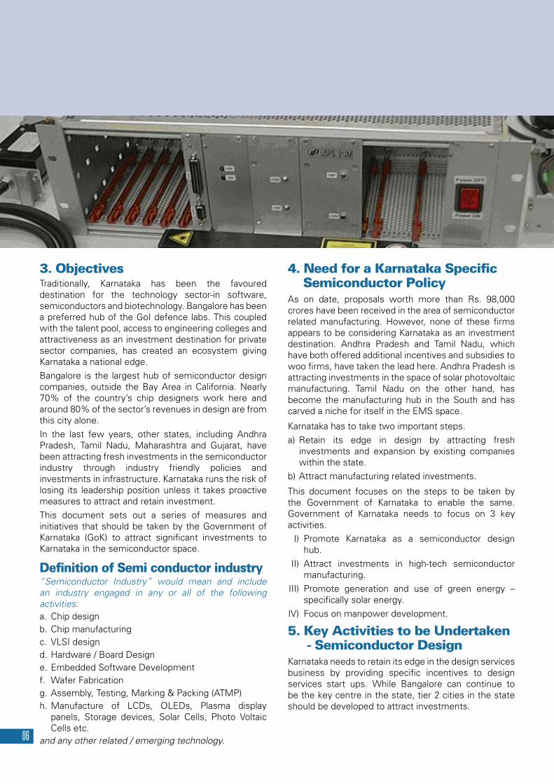
5. Key Activities to be Undertaken - semiconductor DesignKarnataka needs to retain its edge in the design services business by providing specific incentives to design services start ups. While Bangalore can continue to be the key centre in the state, tier 2 cities in the state should be developed to attract investments.
06

5.1. Develop tier 2 cities, satellite towns in Karnataka as Design clustersKarnataka has been the forerunner in the IT/ITeS space owing to an appropriate ecosystem for knowledge-driven industries, including proactive government, sector-friendly policy and a large pool of skilled manpower. IT & ITeS sector accounts for 25% of Karnataka’s Gross State Domestic Product GSDP of $47.32 bn in 2006-2007. As per STPI, semiconductor design and development constitutes a key element of IT revenues.
Apart from Bangalore, the other emerging destinations for the design sector are Mysore, Mangalore and Hubli. Mysore with software export revenues of Rs. 760 crores (US$ 190 mn) is emerging as an alternative destination to Bangalore in service and tourism sectors. 49 firms are registered with the STPI in Mysore. A cargo airport is expected to be commissioned here soon. With the opening up of the 111 km BMIC corridor, travel time is likely to reduce further. Mangalore with software export revenues of Rs.681 crores is a fast emerging hub for logistics, manufacturing and services, with 24 firms currently registered with Mangalore STPI. It also has the added advantage of an international airport and seaport. Hubli is now becoming the choice of IT and ITeS firms with 13 firms registered with STPI and revenues of Rs.0.85 crores. All three cities are centres of educational institutions with 5 major universities being headquartered in these three locations. This cluster generates sizeable revenues from software and its further development should be taken up by the Government of Karnataka.
To encourage setting up of semi conductor units in Tier-2 cities other than Mysore, Mangalore, Hubli an incentive of Investment Promotion Subsidy would be provided in accordance with the Karnataka Industrial Policy 2009-14.
5.2. Incentives for the Design sector5.2.1. Fund for silicon Design start-upsCurrently, the Government of Karnataka renders financial assistance to start-ups through the Karnataka Information Technology Venture Capital Fund (KITVEN Fund).
KITVEN fund is an Information Technology specific Rs. 15 crores, fund registered with Securities & Exchange Board of India (SEBI).
KITVEN Fund helps the early stage investor, extending support services to companies mainly in the areas of financial strategies, business strategies, internal controls, management information system etc. The Fund has invested in 17 companies with investment of more than Rs.12 crores . Some of the assisted companies have grown in size and KITVEN Fund has exited from 13 companies.
This fund should be made available to chip design and embedded software firms too. Limits however could be revised upwards to be in line with investment levels in start up organizations in the industry. A start up firm with 15 employees would need funds in the range of Rs. 2-3 crores in year 1.
Government of Karnataka would provide additional amount of Rs.25 crores, towards 26% contribution to the KITVEN IT Fund for raising funds from the market to assist start up semi-conductor units engaged in design and embedded software.
5.2.2. Financial Assistance towards Patent RegistrationGovernment of Karnataka would provide financial assistance to firms for filing IP in accordance with the incentives provided in the Industrial Policy 2009-2014.
5.2.3. setting up of characterisation Lab at orchid tech spaceSTPI-Bangalore and the Karnataka Government, with support from the industry, were the first in India to open a world-class incubation centre in June 2006, with an investment of Rs. 9.2 crores. The Orchid Tech space integrated incubation centre is meant to create opportunities for entrepreneurs. The state-of-the-art centre, which can support 10 companies at a time, works closely with the Indian Semiconductor Association (ISA) and The Indus Entrepreneurs (TiE) to incubate tech start-ups and firms.
The Government of Karnataka would focus on attracting entrepreneurs to use the state of the art facilities provided by this incubation centre. With the state-of-the-art facilities, including high-end desktops, servers, data centre and an international gateway, the incubation center encourages and facilitates innovation without the constraints of capital investment.
The infrastructure at Orchid Tech space would be augmented to that of a characterization lab, with equipment such as logic analysers, spectrum analysers, oscilloscope, etc, which are required by design.
Government of Karnataka will provide assistance of 50% of the total cost towards purchase of proposed equipment,, for augmenting the Orchid Tech Space in STPI to a Characterisation Lab. The remaining funds would come from the industry or mobilized through PPP business model. This Lab will be a one-stop solution for hi-tech facilities and will spur the growth of R & D in future technology without financial burden to budding entrepreneurs.
07

6. Key Activities to be Undertaken - semiconductor ManufacturingThe semiconductor industry is widely recognised as the key driver for economic growth, besides acting as a technology enabler for the entire electronics value chain. Karnataka would draw up initiatives to set up an entire eco system which would provide the infrastructure and incentives for attracting investments in the areas of Solar PV cell manufacturing; ATMP facilities; Wafer fabrication facility. Building a manufacturing cluster will facilitate development of the industry.
ATMP units will be encouraged with special incentives in the proposed ITIR near BIAL, Bangalore (Special incentives for the ITIR to be announced separately).
6.1 Focus on Attracting Investments in solar PV ManufacturingRationale for promoting investments in solar PV:• Theinvestmentsareloweratabout$200millionfor
a 100 MW line, when compared to semiconductor fabs, which are upward of $ 3 bn
• Solarenergybeingcleanenergycouldattractfurtherinvestments – especially if the government policies are attractive, including the provision of subsidies/incentives based on generation based incentives, equipment used and land.
• Demandforsolarcells/modules/systemsisexpectedto increase, both from export and domestic markets.
Karnataka has a clear early mover advantage in this arena. It has emerged as a hub for the manufacture of solar energy products such as solar water heating systems, solar photovoltaic modules and systems and various components required by the renewable energy sector. With the proactive promotion activities implemented by other states, Karnataka is losing this advantage and could cease to attract further investment. Post the announcement of Government of India’s semiconductor policy and aggressive initiatives shown by neighbouring states, new investors are considering Andhra Pradesh, Tamil Nadu and other states as their destinations for solar PV production. Government of Karnataka hence needs to work towards retaining its leadership position and attracting the large investments announced in this field.
The recent investments seen in solar PV manufacturing are essentially from large players looking at both the domestic and export markets - Reliance, Moser Baer, Signet Solar, Solar Semiconductors, etc. These firms are likely to initially focus on export markets. As the cost of power generation from solar PV route reduces further, India itself could emerge as a market for solar energy, given the high solar incidence in India and the initiatives being taken by the government.
Government of Karnataka would provide all encouragement and assistance to the Solar PV Manufacturing Units under the Karnataka Renewable Energy Policy.
08

6.2 Promote Karnataka as a Destination for AtMP and Ancillary UnitsSemiconductor assembly, testing, marking and packing process (ATMP) is challenging, but is presently a more viable option to front-end manufacturing in India.
Building a state of the art semiconductor fabrication facility requires high capital investment, access to technology, skilled manpower with experience on foundry process and customers willing to devote resources to switch over to a new vendor. A latest estimate states that chip fabrication needs an investment of US $3 bn or more and will continue to go up with each new technology process.
IC assembly involves a different and lower order of complexity than what is required in front end wafer processing. ATMP location and processes are independent of wafer fabrication units and can therefore be located anywhere in the world. Investments vary with the product and capacity and could range anywhere between US $ 100 to 500 mn for large capacity plants.
India offers an advantage in terms of availability of low cost talent and not necessarily only engineers. An ATMP facility in India could import wafers, assemble and after final testing, ship the final device directly to customers - who are largely in Asia itself.
If Karnataka becomes the hub for ATMP facilities, the state would become the preferred destination for the fab companies to invest in chip manufacturing.
Under the Semiconductor Policy of Govt of India, the threshold limit for availing incentives for ATMP is Rs. 1,000 core (US $ 250 mn), which is on the higher side for ATMPs.
To encourage setting up of ATMPs in the State, Government of Karnataka would provide incentives to units set up in the State by lowering the threshold investment for ATMPs. / eco-system units with investment above Rs.400 crores and upto Rs.1000 Crores. Incentives would be provided on a case-to-case basis approach based on specific employment potential.
6.3 Attract Investments for a Wafer Fabrication FacilityWafer fabrication is a highly capital intensive activity and a state of the art wafer fab could cost around $3 bn for a single fabrication unit and assuming a 2:1 debt equity ratio, such a unit could require up to US $ 1 bn in equity investments. Given that India is a late entrant and does not have a ready infrastructure to attract such large investments, strong encouragement from the government is required to draw the first set of investors to commit to such large investments. This will also be viewed as Government’s commitment towards funding the foundation of this sector.
The industry is also characterised by long gestation periods with typical break even periods being in the order of 8-10 years. Government support is very critical in the initial stages.
Setting up a fab facility is likely to result in long term benefits in terms of employment generation, increased inflow of foreign investments into the state and increased manufacturing activity. Each wafer fab facility would result in the establishment of 15 ancillary units. Local semiconductor manufacturing will also spur investments in electronics equipment / products manufacturing.
09
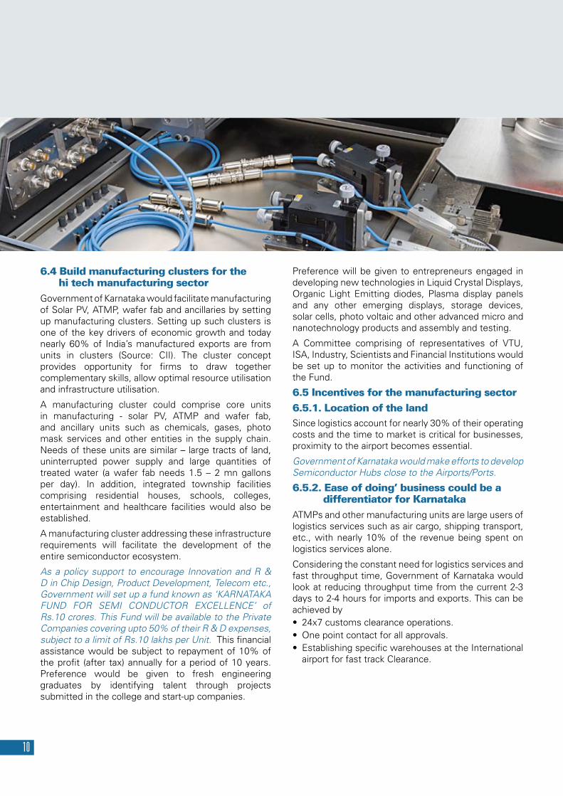
6.4 Build manufacturing clusters for the hi tech manufacturing sectorGovernment of Karnataka would facilitate manufacturing of Solar PV, ATMP, wafer fab and ancillaries by setting up manufacturing clusters. Setting up such clusters is one of the key drivers of economic growth and today nearly 60% of India’s manufactured exports are from units in clusters (Source: CII). The cluster concept provides opportunity for firms to draw together complementary skills, allow optimal resource utilisation and infrastructure utilisation.
A manufacturing cluster could comprise core units in manufacturing - solar PV, ATMP and wafer fab, and ancillary units such as chemicals, gases, photo mask services and other entities in the supply chain. Needs of these units are similar – large tracts of land, uninterrupted power supply and large quantities of treated water (a wafer fab needs 1.5 – 2 mn gallons per day). In addition, integrated township facilities comprising residential houses, schools, colleges, entertainment and healthcare facilities would also be established.
A manufacturing cluster addressing these infrastructure requirements will facilitate the development of the entire semiconductor ecosystem.
As a policy support to encourage Innovation and R & D in Chip Design, Product Development, Telecom etc., Government will set up a fund known as ‘KARNATAKA FUND FOR SEMI CONDUCTOR EXCELLENCE’ of Rs.10 crores. This Fund will be available to the Private Companies covering upto 50% of their R & D expenses, subject to a limit of Rs.10 lakhs per Unit. This financial assistance would be subject to repayment of 10% of the profit (after tax) annually for a period of 10 years. Preference would be given to fresh engineering graduates by identifying talent through projects submitted in the college and start-up companies.
Preference will be given to entrepreneurs engaged in developing new technologies in Liquid Crystal Displays, Organic Light Emitting diodes, Plasma display panels and any other emerging displays, storage devices, solar cells, photo voltaic and other advanced micro and nanotechnology products and assembly and testing.
A Committee comprising of representatives of VTU, ISA, Industry, Scientists and Financial Institutions would be set up to monitor the activities and functioning of the Fund.
6.5 Incentives for the manufacturing sector6.5.1. Location of the landSince logistics account for nearly 30% of their operating costs and the time to market is critical for businesses, proximity to the airport becomes essential.
Government of Karnataka would make efforts to develop Semiconductor Hubs close to the Airports/Ports.
6.5.2. ease of doing’ business could be a differentiator for KarnatakaATMPs and other manufacturing units are large users of logistics services such as air cargo, shipping transport, etc., with nearly 10% of the revenue being spent on logistics services alone.
Considering the constant need for logistics services and fast throughput time, Government of Karnataka would look at reducing throughput time from the current 2-3 days to 2-4 hours for imports and exports. This can be achieved by• 24x7customsclearanceoperations.• Onepointcontactforallapprovals.• EstablishingspecificwarehousesattheInternational
airport for fast track Clearance.
10

6.5.3. Industrial parks focussed on semiconductor design and manufacturing sectorGovernment of Karnataka would set up industrial parks/ SEZs under public private partnership (PPP) model or with other governments, along the lines of the Suzhou Park, China and Hscinchu Park in Taiwan. Some of the features and benefits that would be provided:
• Attractiveworkingenvironmentandlivingconditions,proximity to technical expertise, design and manufacturing facilities to units setting up operations in the Park
• Beinggovernment-owned, it alsooffersa rangeofspecial benefits such as:• lowrentsonland.• low-interestgovernmentloans.• R&Dmatchingfunds.• taxbenefits.• special exemptions from tariffs, commodity and
business taxes.• Governmentpurchaseoftechnologyfromabroad
for transfer to participating companies.• access to government laboratories and test
facilities in the Park.
This would be specifically promoted for semiconductor design and manufacturing firms. A lease share on sites would be offered to organizations on the basis of number of employees and revenues generated. Initial lease share on sites would meet the growth requirements of next 3 years. Companies not interested in a lease share on land could opt for a lease of ready and furnished office spaces ranging from business suites of 1000 sft (square feet) for start-ups to larger office space of up to 50,000 sft. Lease share in the land or office would be allocated to organizations for their own use and not for sub leasing. Support infrastructure of water, waste water treatment plants, power back up, connectivity, etc. would be provided by the Government of Karnataka.
This would be actively promoted by the State Government while preparing the Master plan for the proposed Information Technology Investment Region near BIAL, Bangalore.
11

7. Key Activities to be Undertaken to Promote Green energyIndia receives 4-7 KWh/day/square meter of solar energy averaged over a year. The amount of solar energy that India receives in a few minutes is more than India can consume in a whole year. With the power crisis and shortage of fuel fossil, it is imperative to promote green energy.
Government of Karnataka would focus on building capacities for solar power generation and increase consumption of solar power by residential and industrial users.
7.1 Promote Development of solar FarmsSolar farms are a source of commercial solar power. Government of Karnataka would look at encouraging development of solar farms. Some of the measures that would be considered for promoting establishment of solar farms.
Karnataka Power Corporation and Karnataka Renewable Energy Development Limited would take steps to develop Solar Farms on Joint Venture / PPP mode in Bijapur, Gulbarga, Raichur and Bellary districts.
7.2. encourage use of solar energyWhile promoting solar cell manufacturing, Government of Karnataka would also popularize solar energy usage among households, and commercial establishments. This will result in a large domestic demand for solar based products. Differential tariffs of power for “luxury use” like malls, billboards, etc. would be taken up with the State Electricity Regulatory Commission (SERC).
Today Germany is at the forefront of solar PV production as well as solar power generation primarily because of the measures taken by the government.
Government of Karnataka would encourage additional measures while continuing with the incentives provided by Karnataka Renewable Energy Development Corporation Ltd.
• Encourage Corporate sponsored programs underthe Education Policy, where every school is powered with solar, which will result in increased utilisation of computers by students.
7.3. ‘core group’ to Promote the cause of solar in the GovernmentGovernment of Karnataka would look at forming a core group in the Government to promote solar PV industry. The core group would be responsible for liaising with the various stakeholders in the industry, set solar energy targets for the government and address issues that arise.
Provide impetus to R&D programmes like Germany and Japan, which are expected to reduce the cost of PV modules and improving efficiency of the systems.
12
8. Focus on Manpower Development8.1. need to Build Domain expertiseManpower development is critical to the semiconductor industry. There is need for India to build its domain expertise in the area of manufacturing. This can be achieved only if the government focuses on training its engineering graduates and diploma holders. Training can either be as an internship program where the trainee is trained on the job or through special institutes set up for the process.
8.1.1. Institute a Focussed Program Under IIItThe growth of the IT sector in the initial years was aided by the establishment of training institutes like NIIT and Aptech, which helped in creating awareness and popularising the sector. There is need for similar institutes that would focus on providing training on semiconductor design and manufacturing.
Government would establish a focussed school under IIIT that would offer courses specific to semiconductor manufacturing
In addition, Government of Karnataka would also look at strengthening and enhancing its existing engineering colleges and polytechnics. Align the semiconductor laboratories at the institutes with industry standards: The government and the industry would channelize funds to improve the infrastructure at research laboratories so that they are equivalent to industry standards. For instance, research in Indian institutes is being carried out at 130nm, whereas the industry is working on 45nm. There is a need to bridge this gap by developing and maintaining the requisite research facilities. (ISA- Evalueserve study 2008)
Government to set-up a focussed school under IIIT at a cost of Rs. 10 crores and strengthen the Research Labs in the institute at a cost of Rs. 5 crores, with a contribution of 25% from the industry.
13

9. Fiscal Incentives Fiscal Incentives under Karnataka Industrial Policy
2009-2014 (Incentives to units located in Zone 4 would be as applicable to Zone 3).
Package of Incentives and Concessions offered for Investments
1. Investment Promotion subsidy a) Micro Mfg. Enterprises
Zone – 1 : 25% VFA (max. Rs.10 lakhs) Zone – 2 : 20% VFA (max. Rs.7.5 lakhs) Zone – 3 : 15% VFA (max. Rs.5.00 lakhs) Zone – 4 : Nil
b) Small Mfg. Enterprises Zone – 1 : 20% VFA (max. Rs.20 lakhs) Zone – 2 : 15% VFA (max. Rs.15 lakhs) Zone - 3 : 10% VFA (max.Rs.10 lakhs) Zone – 4 : Nil
c) Med. Mfg. Enterprises (Those who employ minimum 25 workers)
Zone – 1 : Rs.30 lakhs Zone – 2 : Rs.20 lakhs Zone – 3 : Nil Zone – 4 : Nil
Notes :
(i) 25% of the subsidy sanctioned amount will be released every year on refund basis towards the payments made by the unit in respect of gross VAT, ESI and PF and power tariff.
In cases of enterprises which do not use power and not covered under VAT, EPF, ESI the investment subsidy will be released against the loan dues.
(ii) This incentive is available to enterprises availing term loan to an extent of minimum 50% cost of fixed assets only.
(iii) The unit shall avail the sanctioned subsidy within the period of five years.
1.1 Additional subsidy to SC/ST, Women, Physical challenged, Ex-Servicemen Entrepreneurs and enterprises coming up in most Backward taluks of Hyderabad Karnataka region.
Additional 5% subsidy subject to a maximum of Rs.1.00 lakh, Rs.3.00 lakhs and Rs.5.00 lakhs for Micro, Small and Medium Manufacturing Enterprises respectively.
2. exemption from stamp Duty
MSME, Large and Mega Projects : Stamp duty to be paid in respect of (i) loan
agreements, credit deeds, mortgage and hypothecation deeds executed for availing term loans from State Govt. and / or State Financial Corporation, Industrial Investment Development Corporation, National Level Financial Institutions, Commercial Banks, RRBs, Co-operative Banks, KVIB / KVIC, Karnataka State SC/ST Development Corporation, Karnataka State Minority Development Corporation and other institutions which may be notified by the Government from time to time for the initial period of five years only and (ii) for lease deeds, lease-cum-sale and absolute sale deeds executed by industrial Enterprises in respect of industrial plots, sheds, industrial tenements, by KIADB, KSSIDC, KEONICS, Industrial Co-operatives and approved private industrial estates shall be exempted as below :
Zone – 1 : 100% Zone – 2 : 100% Zone – 3 : 75% Zone – 4 : Nil
3. concessional Registration charges MSME, Large and Mega Projects: For all loan documents and sale deeds as specified
in 2 above, the registration charges shall be at a concessional rate of Re.1 per Rs.1000.
Note :
(i). The exemption of stamp duty and concessional registration charges are also applicable to lands purchased under Section 109 of the KLR Act and also for direct purchase of industrially converted lands for the projects approved by SHLCC / SLSWCC / DLSWCC. This incentive will also be applicable for the land transferred by KIADB to land owners as compensation for the acquired land.
(ii) The exemption of stamp duty and concessional registration charges are also available for registration of final sale deed in respect of lands, sheds, plots, industrial tenements after the expiry of lease period at the rate as specified in the Industrial Policy which was in vogue at the time of execution of lease-cum-sale deed.
14

4. Waiver of conversion Fine MSME, Large and Mega Projects : The payment of conversion fee for converting the
land from agriculture use to industrial use including for development of industrial areas by private investors will be waived as detailed below:
Zone – 1 : 100% Zone - 2 : 100% Zone – 3 : 75% Zone - 4 : Nil
Note:
The waiver of conversion fine will be on reimbursement basis after implementation of projects.
5. exemption from entry tax MSME, Large and Mega Projects : In Zone – 1, 2 and 3 :
100% exemption from payment of ET on ‘Plant & Machinery and Capital Goods’ for an initial period of 3 years from the date of commencement of project implementation. For this purpose, the term ‘Plant & Machinery and Capital Goods’ also includes Plant & Machinery, equipment etc. including machineries for captive generation of Electricity.
On raw materials, inputs, component parts & consumables (excluding petroleum products) [wherever applicable] for a period of 5 years from the date of commencement of commercial production.
Zone – 4 : Nil
6. Incentives for exported oriented enterprises
MSME, Large and Mega Projects :(i) Exemption from payment of ET
For 100% EOUs, 100% exemption from payment of ET on ‘Plant & Machinery and Capital Goods’ for an initial period of 3 years from the date of commencement of project implementation irrespective of zones.
For other EOUs, (Minimum Export obligation of 25%of their total turnover) 100% exemption from payment of ET on raw materials, inputs, component parts & consumables (excluding petroleum products) for an initial period of 3 years from the date of commencement of commercial production in Zone 1, 2, and 3 and 50% in Zone 4.
(ii) Refund of Certification Charges :
Refund of expenses incurred for compulsory marking like Conformity Europeenne (CE), China Compulsory Certificate (CCC), etc., to the extent of 50% of expenses subject to a maximum of Rs. 2.00 lakhs per unit for both 100% and other EOUs in all zones.
7. subsidy for setting up etPs MSME, Large and Mega Projects : One time capital subsidy upto 50% of the cost
of Effluent Treatment Plants (ETPs), subject to a ceiling of Rs.100 lakhs per manufacturing enterprise in Zone – 1, 2 & 3 and a ceiling of Rs.50 lakhs in Zone – 4.
15

8. Interest Free Loan on VAt Large and Mega Projects : All new large and mega manufacturing Enterprises
established in Zone – 1, 2 and 3 shall be offered interest free loan on VAT as specified below:
Investment range on fixed assets (Rs. Cr.)
Min. Direct Emp. (Nos.)
Quantum of interest free loan
10 (value of plant & machinery) – 50
Minimum 100 employ-ment and additional 20 employment for every Rs.10 cr. investment.
50% of assessed gross VAT for initial 5 yrs. subject to the max. of 100% of total value of fixed assets.Repayment of the loan shall be in 3 annual installments after 5 yrs.
51 – 250 Minimum 200 employment and additional 20 employment for every Rs. 50 cr. investment.
50% of assessed gross VAT for initial 6 yrs. subject to the max. of 75% of total value of fixed assets.Repayment of the loan shall be in 3 annual installments after 6 yrs.
251 - 1000 Minimum 400 up to Rs.300 Crs and 50 additional employment for every Rs.100 Crs additional investment
25% of assessed gross VAT for initial 7 yrs. subject to the max. of 50% of total value of fixed assets.Repayment of the loan shall be in 4 annual installments after 7 yrs.
1001 - 3000 Minimum 750 for Rs 1000 Crs and additional 25 for every Rs.100 Crs additional investment
25% of assessed gross VAT for initial 10 yrs. subject to the max. of 50% of total value of fixed assets. Repayment of the loan shall be in 4 annual installments after 10 yrs.
More than 3000
1250 25% of assessed gross VAT for initial 15 yrs. subject to the max. of 50% of total value of fixed assets. Repayment of the loan shall be in 5 annual in-staments after 12 yrs.
Zone – 4 : Nil
9. Anchor Unit subsidy Anchor unit subsidy of Rs.100 lakhs shall be
offered for the first two manufacturing Enterprises with minimum employment of 100 members and minimum investment of Rs.50 crores in each of the taluks coming in Zone-1, 2 & 3 will be offered. This subsidy will be applicable only in taluks where no industrial Enterprises with investment of Rs.50 crores and above exist at present.
10. special incentives for enterprises coming up in low HDI districts
Only for Large & Mega Projects : New large scale Enterprises setting up facilities
in six districts having bottom most Human Development Index (HDI) and employing atleast 75% local persons as defined in the Sarojini Mahishi recommendations will be offered 75% reimbursement of expenditure on account of contribution towards Employees State Insurance (ESI) and Employees Provident Fund (EPF) scheme for a period of initial five years.
However, these benefits over a period of five years will be limited to 25% of value of fixed capital investment. The amount of reimbursement will be paid annually based on minimum statutory limit subject to the condition that the unit has paid its contribution towards ESI & EPF on the due dates. Following are the six districts having bottom most Human Development Index:
Sl. No.
District HDI* (2001)
1. Bagalkot 0.591
2. Bijapur 0.589
3. Koppal 0.582
4. Chamarajanagar 0.576
5. Gulbarga 0.564
6. Raichur 0.547
*As per Karnataka Human Development Report - 2005 published by the Department of Planning & Statistics, Government of Karnataka.
16

17Govt of Karnataka acknowledges the valuable inputs given by
ISA in the preparation of this policy document.
11. Interest subsidy Micro manufacturing enterprises : Interest subsidy @ 5% on term loans. The interest subsidy is payable
only on the interest actually paid to financial institutions and not defaulted in payment of principle or interest installments. The amount of interest subsidy will be effective rate of interest (after deducting interest subsidy) receivable by any institutions / under any Govt. of India scheme or 5% per annum whichever is less). The period of interest subsidy is 5 years, 4 years and 3 years in Zone -1, Zone 2 and Zone 3 respectively.
12. exemption from electricity Duty Micro & Small Mfg. Enterprises : 100% exemption of electricity duty / tax for the initial period of five years,
four years and three years in Zone – 1, Zone-2 and Zone-3 respectively.
13. technology Upgradation, Quality certification and Patent Registration Micro & Small Mfg. Enterprises :
(i) Interest Subsidy on TU Loan : Zone 1, 2 & 3 : 5 % on loans availed from KSFC, KSIIDC & Scheduled commercial banks, which are not covered under CLCSS of GOI.
(ii) ISO series certification : Zone 1, 2, 3 & 4 : 75% of cost (max. Rs.75,000). (iii) BIS Certification: 50% of fees payable to BIS. (max. Rs.20,000) and 25% of cost (max.Rs.50,000) for
purchase of testing equipments as approved by BIS.(iv) Patent registration : 75% of cost of fees payable to Patent Office (max. Rs.1.25 lakhs) and 50% of cost
(max. Rs.75,000) towards attorney fees, patent search etc. (v) Technology Adoption : 25% of cost (max. Rs.50,000) for adopting technology from recognized national
laboratories. (vi) Technology Business Incubation Centre : 25% of the project cost (Max : Rs.50 lakhs).
14. Water harvesting / conservation Measures Small & Medium Mfg. enterprises in all Zones.
(i) Rain water harvesting : 50% of cost (max. Rs. 1 lakh).(ii) Waste water recycling : 50% of cost (max. Rs. 5 lakh). (iii) Zero discharge process : 50% of cost (max. Rs. 5 lakh).
15. energy conservation Small & Medium mfg. enterprises in all zones. Practicing Energy Conservation measures resulting in reduction of Energy Consumption of atleast 10% of
earlier consumption: 10% of capital cost (max Rs.5 lakh).
Use of non-conventional energy sources: 10% of capital cost (max. Rs.5 lakh).
16. Addl. Incentives to the enterprises following Reservation Policy of the state Medium, Large and Mega Manufacturing Enterprises in all zones employing more than 100 persons :
50% reimbursement of expenditure incurred for employees coming under reserved category towards contribution to ESI & EPF schemes for a period of initial 5 years.
17. Refund of cost incurred for preparation Project Reports Micro & Small Mfg. Enterprises : Zone 1, 2 & 3 : The cost incurred for preparation of project reports
by TECSOK/CEDOK/KSFC or any other recognized institutions for availing loans shall be reimbursed to the maximum of Rs.10,000/- per unit subject to financing of the unit.
effective Date :This Policy shall come into force with effect from the date of issue of the Government Order in this regard and shall remain in force for a period of five years from such date or till the issue of a new or revised Semiconductor Policy.
For Information and Assistance, please contact
Principal Secretary to the GovernmentDepartment of Information Technology, Biotechnology and Science & Technology
Government of Karnataka6th Floor, 5th Stage, M.S. Building, Bangalore - 560 001, Karnataka, India.
•Ph: +91-80-2228 0562 / 2226 5943 •E-mail: [email protected]
Managing DirectorKarnataka Biotechnology & Information Technology Services# 9, 2nd Floor, UNI Building, Thimmaiah Road, Vasant Nagar
Bangalore - 560 052, Karnataka, India.•Ph: +91-80-2220 7006 / 2237 0309 •Fax: +91 80 4132 7510
•E-mail: [email protected]
Visit : www.bangaloreitbt.in
“The Semiconductor industry has come a long way from the West to low cost locations in Asia, where memory production and backend
operations have shifted. Over 70% of the total Semiconductor sales would be driven by the Asian consumers of computers, LCD TVs, Blu-
ray players, Smart phones, Net books, Medical devices etc.”
Sri Ashok Kumar C. Manoli, IAS, Principal Secretary to Govt Department of IT, BT and S&T