Kamera CCD Astronomi (2) AS3100 Lab. Astronomi Dasar I Prodi Astronomi 2007/2008 B. Dermawan.
21
Kamera CCD Astronomi (2) AS3100 Lab. Astronomi Dasar I Prodi Astronomi 2007/2008 B. Dermawan
-
Upload
kellie-godin -
Category
Documents
-
view
254 -
download
19
Transcript of Kamera CCD Astronomi (2) AS3100 Lab. Astronomi Dasar I Prodi Astronomi 2007/2008 B. Dermawan.

Kamera CCD Astronomi (2)
AS3100 Lab. Astronomi Dasar IProdi Astronomi 2007/2008
B. Dermawan

Clocks
CCD detector
Amplifier
Digital converter
Cooling system Input/
Output interface
ComputerPhotons
ADUs
Images
Acquisition command
CCD Camera Control
Malasan

CCD Spectral Response (Sensitivity)
Majewski

Quantum Efficiency (QE)
• Peak QEs for CCDs are 40-80%• Vary with wavelength• Important source of variation: the ability of photons
of different wavelengths to penetrate the silicon• Flux at some depth of the silicon:
is the coefficient of intrinsic absorption
Majewski
zeFzF )0()(
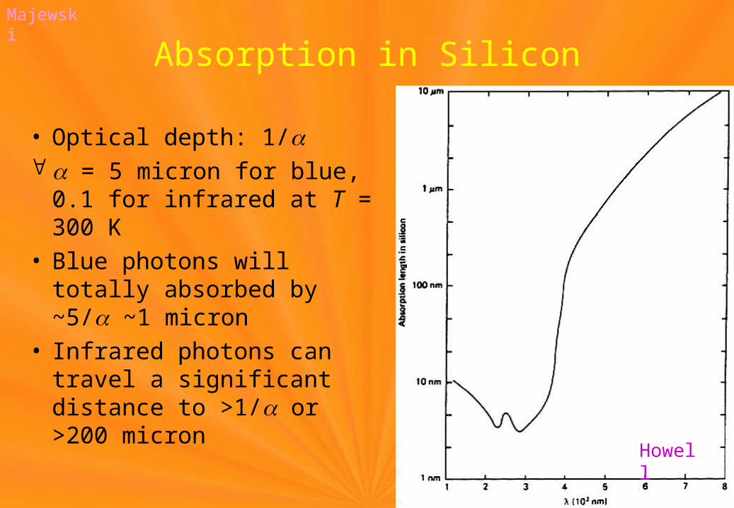
Absorption in Silicon
• Optical depth: 1/ = 5 micron for blue, 0.1
for infrared at T = 300 K• Blue photons will totally
absorbed by ~5/ ~1 micron
• Infrared photons can travel a significant distance to >1/ or >200 micron
Howell
Majewski

CCDs Red and Blue Limits of Sensitivity
• Sensitivity in red requires substrate thick enough to have enough opportunity to absorb weakly interacting red photons
Thick CCDs (frontside illuminated)• Sensitivity in the blue is limited by weak penetration
of photons (on order of only microns). Need to be worried about thinness of SiO2 and other layers to cross. To increase the efficiency in blue, decrease thickness of Si to be crossed
Thin CCDs (backside illuminated)
Majewski

Frontside CCDsEasier to make (cheap)Thick substrate and surface layers OK for red photons to ~11,000 Å
low, can travel 500 micron or more The thicker the CCD, the more sensitive However: loss of resolution with increasing thickness,
more substrate = more chances for dark current
Majewski
Frontside CCDs
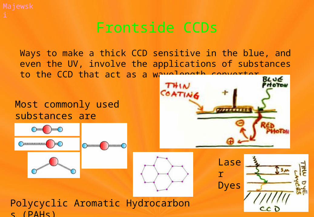
Ways to make a thick CCD sensitive in the blue, and even the UV, involve the applications of substances to the CCD that act as a wavelength converter
Most commonly used substances are fluorescent
Polycyclic Aromatic Hydrocarbons (PAHs)
Laser Dyes
Majewski

Frontside CCDs: ExampleMajewski
Backside CCDs
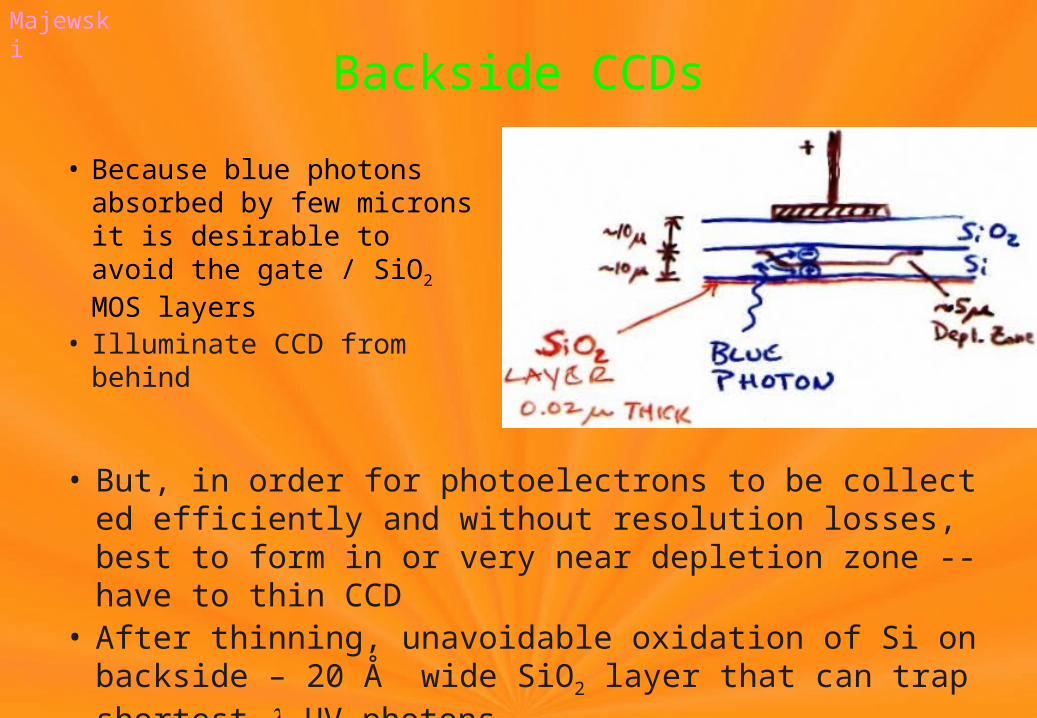
• Because blue photons absorbed by few microns it is desirable to avoid the gate / SiO2 MOS layers
• Illuminate CCD from behind
• But, in order for photoelectrons to be collected efficiently and without resolution losses, best to form in or very near depletion zone -- have to thin CCD
• After thinning, unavoidable oxidation of Si on backside – 20 Å wide SiO2 layer that can trap shortest UV photons
Majewski

QE vs WavelengthMajewski
Frontside & backside illuminations

Notes on CCDsBias Level
• Due to the readnoise problem, it is possible for a normal CCD pixel to have a (slightly) negative value
• Other effects can also yield negative output values for normal pixels
• To properly account for this problem, but get the substantial dynamic range benefit of 16 bit unsigned output, CCD electronics will add a pedestal level, called the bias level, to shift all pixel levels up into the positive range
• This "zero" level is typically a few hundred to ~1000 ADU
Howell
Majewski
Notes on CCDs
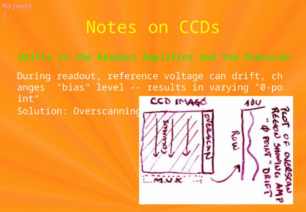
Drifts in the Readout Amplifier and the Overscan During readout, reference voltage can drift, changes "bias" level -- results in varying "0-point“Solution: Overscanning
Majewski

Notes on CCDsLinearity
Majewski
For a given pixel, let: F be the incident flux (in photons per second) S be the recorded signal level (in ADU) Q be the quantum efficiency G be the gain t be the integration time (in seconds) Then, for a strictly linear system:
FtG
QS
In reality, Q is a function of the accumulated charge:
t
dttSQQ0
)(

Notes on CCDsBlooming
Majewski
Depends very much on the electronic design of the CCDDuring readout, not all the charge can be shifted – some is left behind (streaks –blooming or blending-- forming behind saturated pixels
This can be minimized somewhat by the inclusion of electronic “drains” in the CCD, called an Anti-Blooming Gate (ABG)However, also drains off wanted charge and so reduces the QE of the device

Notes on CCDs
Dynamic RangeThe dynamic range of a CCD is limited by its maximum useful level (the full well capacity (FWC) is an ultimate limit for a pixel)
Adopting the definition use din acoustics, the dynamic range, D, of a CCD is given in decibels by:
D(db) = 20 log10 (maximum level / RN )
A CCD with 100,000 e- = FWC and RN = 10 e- has an 80 dB dynamic range
Majewski

Notes on CCDsCosmetic DefectsDead pixel - Pixel unresponsive to light due to defective gate, depletion zone, substrate, insulator, etc.
Hot pixel - Pixel with much larger dark current than neighbors
Bad column - A defective pixel where the defect affects CTE and all charge packets that pass through the defective pixel will be destroyed (e.g., fall into a trap) resulting in a bad column in the final image
Majewski

Notes on CCDs
ElectroluminescenceIn some cases, diodes in the output amplifier can actually act as Light Emitting Diodes (LEDs) and can cause serious problems of excess light near the amplifier
Majewski

Notes on CCDs
Other "Defects" in CCD Images Not Related to Chip Itself
• Dust
Majewski
• Interference
• Sky pollution
• “Cosmic pollution“
• Fringing

Notes on CCDsRadiation Damage in Space CCDsThe harsh radiation environment in space can temporarily or permanently degrade the performance (e.g., the CTE) of a CCD:Solar wind, solar flares and the general background of cosmic high energy particles in unprotected environment away from EarthThe South Atlantic Anomaly (SAA) is the point on the Earth's surface where its inner van Allen belt comes closest
http://www.astro.psu.edu/users/niel/astro485/lectures/lecture09-overhead02.jpg srag-nt.jsc.nasa.gov/AboutSRAG/What/What.htm
Majewski

Advantages of CCDs
The increase in QE over film is like making a telescope into a much bigger one –effectively allowing a 1-m telescope to perform like a 4-m
The accuracy of CCDs in both linearity and stability means the measurements made are of the highest quality, and a wider band of the spectrum is utilised
The digital nature of CCDs allows new techniques to be devised, both in taking the data and extracting the most from it
Majewski


![Asteroid Resonances [1] Kuliah AS8140 Fisika Benda Kecil Tata Surya dan AS3141 Benda Kecil dalam Tata Surya Budi Dermawan Prodi Astronomi 2006/2007.](https://static.fdocuments.in/doc/165x107/56649cce5503460f94999a1d/asteroid-resonances-1-kuliah-as8140-fisika-benda-kecil-tata-surya-dan-as3141.jpg)