K9GDT 40m CW/SSB Receiver - qsl.net · 2-8 BFO Generator ... IF Frequency 3.395MHz Power...
15
K9GDT K9GDT 40m 40m CW/SSB CW/SSB Receiver Receiver by George!
Transcript of K9GDT 40m CW/SSB Receiver - qsl.net · 2-8 BFO Generator ... IF Frequency 3.395MHz Power...
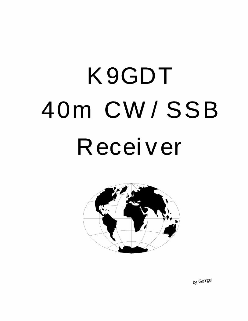
K9GDTK9GDT40m 40m CW/SSBCW/SSB
ReceiverReceiver
by George!
Contents
Introduction1-1 Description of Receiver ....................................................................................................................1-2 Specifications ...................................................................................................................................
Circuit Description2-1 Bandpass Filter ................................................................................................................................2-2 Mixer - Post Mixer Amplifier ...........................................................................................................2-3 Crystal Filter - IF Amplifier - AGC Module .....................................................................................2-4 400Hz Noise Filter/ Product Detector Module ..................................................................................2-5 Audio Processing Board - AF Power Amplifier ...............................................................................2-6 VFO .................................................................................................................................................2-7 LO - Passband Generator Module .....................................................................................................2-8 BFO Generator ..................................................................................................................................2-9 Display Module ................................................................................................................................2-10 Power Supply ...................................................................................................................................
Alignment and Calibration3-1 Required Test Equipment ..................................................................................................................3-2 VFO ..................................................................................................................................................3-3 LO - Passband Generator Module ......................................................................................................3-4 BFO Generator ................................................................................................................................ 3-5 Bandpass Filter ...............................................................................................................................3-6 Mixer - Post Mixer Amplifier ..........................................................................................................3-7 Crystal Filter - IF Amplifier - AGC Module ....................................................................................3-8 Audio Processing Board .................................................................................................................3-9 Display Module ...............................................................................................................................
IllustrationsFigure 1-1 The K9GDT 40m Receiver .....................................................................................................Figure 2-1 Receiver Block Diagram ........................................................................................................Figure 2-2 Front Panel Controls ..............................................................................................................Figure 2-3 Rear Panel Controls and Connections .....................................................................................Figure 2-4 Interior Views - Module Locations ........................................................................................Figure 3-1 LO - Passband Generator Module ...........................................................................................Figure 3-2 BFO Generator .....................................................................................................................
Figure 3-3 Crystal Filter - IF Amplifier - AGC Module .........................................................................Figure 3-4 Audio Processing Board .......................................................................................................Figure 3-5 Display Module ....................................................................................................................
ii
1
2
3345566667
999
101010111213
137789
10111213
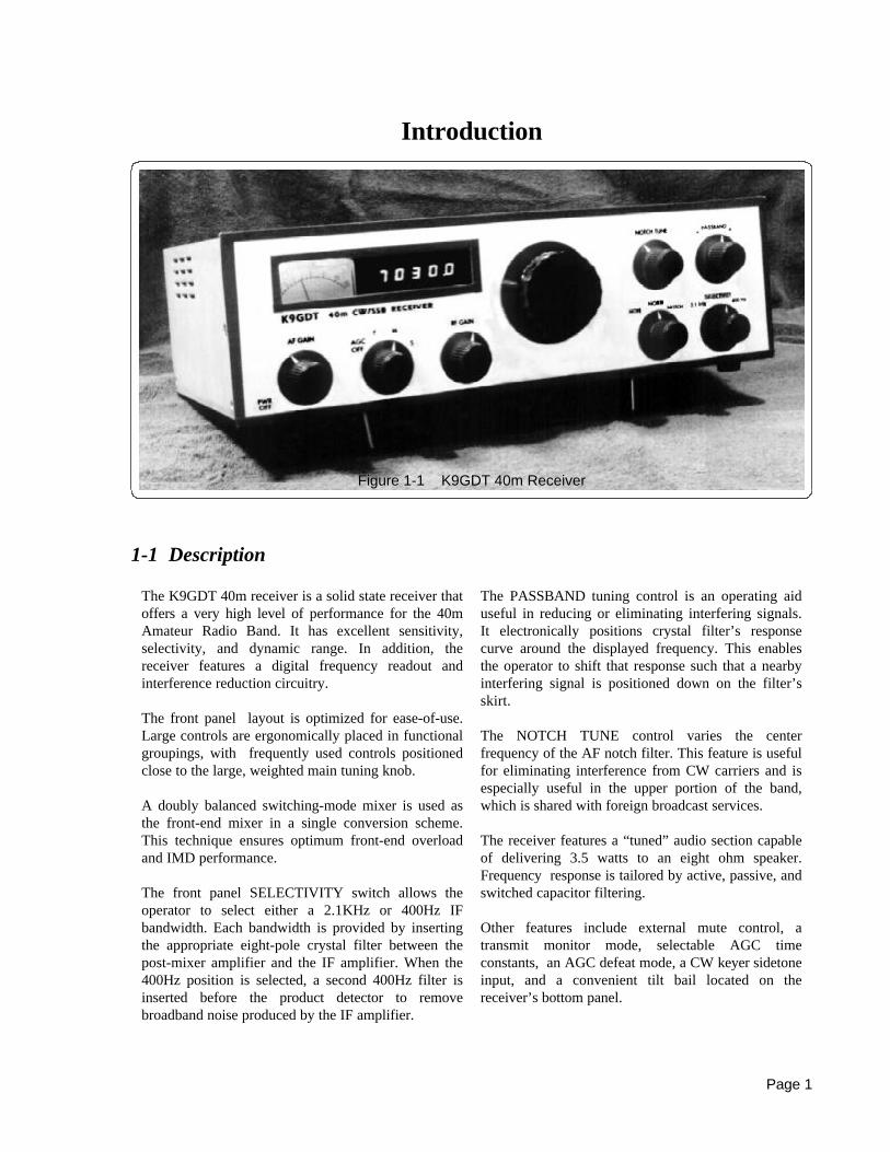
Introduction
1-1 Description
The K9GDT 40m receiver is a solid state receiver thatoffers a very high level of performance for the 40mAmateur Radio Band. It has excellent sensitivity,selectivity, and dynamic range. In addition, thereceiver features a digital frequency readout andinterference reduction circuitry.
The front panel layout is optimized for ease-of-use.Large controls are ergonomically placed in functionalgroupings, with frequently used controls positionedclose to the large, weighted main tuning knob.
A doubly balanced switching-mode mixer is used asthe front-end mixer in a single conversion scheme.This technique ensures optimum front-end overloadand IMD performance.
The front panel SELECTIVITY switch allows theoperator to select either a 2.1KHz or 400Hz IFbandwidth. Each bandwidth is provided by insertingthe appropriate eight-pole crystal filter between thepost-mixer amplifier and the IF amplifier. When the400Hz position is selected, a second 400Hz filter isinserted before the product detector to removebroadband noise produced by the IF amplifier.
The PASSBAND tuning control is an operating aiduseful in reducing or eliminating interfering signals.It electronically positions crystal filter’s responsecurve around the displayed frequency. This enablesthe operator to shift that response such that a nearbyinterfering signal is positioned down on the filter’sskirt.
The NOTCH TUNE control varies the centerfrequency of the AF notch filter. This feature is usefulfor eliminating interference from CW carriers and isespecially useful in the upper portion of the band,which is shared with foreign broadcast services.
The receiver features a “tuned” audio section capableof delivering 3.5 watts to an eight ohm speaker.Frequency response is tailored by active, passive, andswitched capacitor filtering.
Other features include external mute control, atransmit monitor mode, selectable AGC timeconstants, an AGC defeat mode, a CW keyer sidetoneinput, and a convenient tilt bail located on thereceiver’s bottom panel.
Page 1
Figure 1-1 K9GDT 40m Receiver
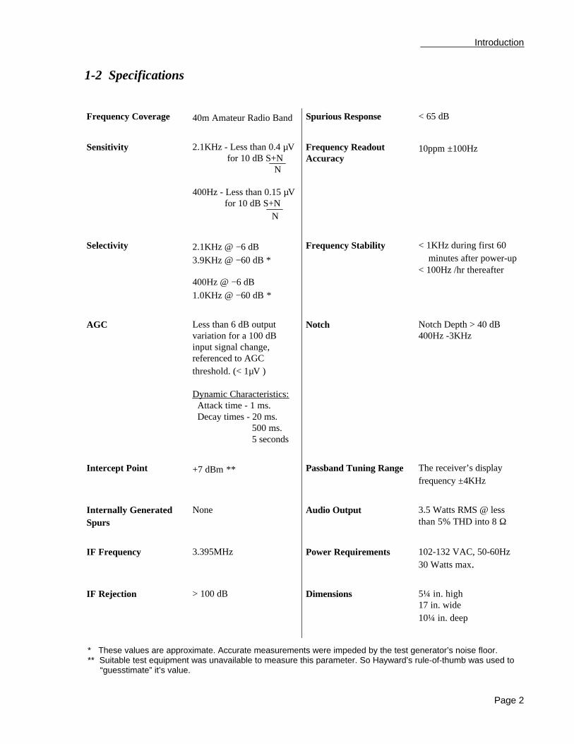
1-2 Specifications
18½ lb.Weight> 60 dBImage Rejection
5¼ in. high17 in. wide10¼ in. deep
Dimensions> 100 dBIF Rejection
102-132 VAC, 50-60Hz30 Watts max.
Power Requirements3.395MHzIF Frequency
3.5 Watts RMS @ lessthan 5% THD into 8 Ω
Audio OutputNoneInternally GeneratedSpurs
The receiver’s displayfrequency ±4KHz
Passband Tuning Range+7 dBm **Intercept Point
Notch Depth > 40 dB 400Hz -3KHz
NotchLess than 6 dB outputvariation for a 100 dBinput signal change,referenced to AGCthreshold. (< 1µV )
Dynamic Characteristics: Attack time - 1 ms. Decay times - 20 ms. 500 ms. 5 seconds
AGC
< 1KHz during first 60 minutes after power-up< 100Hz /hr thereafter
Frequency Stability2.1KHz @ −6 dB
3.9KHz @ −60 dB *
400Hz @ −6 dB
1.0KHz @ −60 dB *
Selectivity
10ppm ±100HzFrequency ReadoutAccuracy
2.1KHz - Less than 0.4 µV for 10 dB S+N N
400Hz - Less than 0.15 µV for 10 dB S+N N
Sensitivity
< 65 dBSpurious Response40m Amateur Radio Band Frequency Coverage
Introduction
Page 2
* These values are approximate. Accurate measurements were impeded by the test generator’s noise floor.** Suitable test equipment was unavailable to measure this parameter. So Hayward’s rule-of-thumb was used to “guesstimate” it’s value.

Circuit Description
2-1 Bandpass Filter Module
The Bandpass Filter module has an input and outputimpedance of 50Ω and consists of two major sections: a dual resonator parallel tuned bandpass filter and a
seven element low pass filter for additionalattenuation of image frequencies from 13.79 through14.09MHz. The module’s insertion loss is under 1dB.
2-2 Mixer - Post Mixer Amplifier
Introduction
Page 3
Figure 2-1 Receiver Block Diagram
The mixer stage is a doubly-balanced diode-ringdevice made by Mini-Circuits Laboratories, modelSBL-1. The 10.395-10.695MHz local oscillator drivelevel is +7dBm.
A 6 dB pad is placed between the mixer output andthe post-mixer amplifier, which is a low noise, highdynamic range broadband bipolar amplifier with a50Ω input impedance. This arrangement assures aproper non-reactive termination at the mixer’s IF portfor all frequencies present, thereby preserving it’s
IMD performance and eliminating the requirement fora diplexer. Because a very low noise figure isnormally not necessary around 7MHz, the pad’s 6 dBinsertion loss is tolerable.
The post-mixer amplifier has a gain of 20 dB using anNTE278 transistor, which has an fT of 1.2 GHz and anoise figure of about 4 dB. This device is heat sunkand biased to a standing current of 70 ma. Theamplifier’s output is matched to the 2 kΩ inputimpedance of the crystal filter which follows.
Display Mixer - 40673
FrequencyCounter7216C
7258.0
L.O.
BFO
K9GDT 40m CW/SSB Receiver
by George!
A.F. Amplifier3.5W 8Ω7-7.3 MHz
First MixerSBL-1
Low NoisePost MixerAmplifier
2.1 kHz
400Hz
3.395 MHz8 pole
Crystal Filters500HzFilter
Gain EQ
MC1350
I.F.Amplifier
AGC
400Hz
-6dbPad
Post I.F.400Hz Filter Product
DetectorMC1496
Tuneable AFNotch
400-3000 Hz
SwitchedCapacitorL. P. Filter
3.0 kHz10.395-10.695 MHz+7dbm
LO Pre-mixSBL-1
4395 ±4 KHz
AC
6-6.3 MHz
Main TuningBFO
3395 ±4 KHz
AGC5.2v no signal5.7v -10 dbm
40673x2
SK3218 LPF
S-meter
-6 db
1 MHz
SBL-1
AC
Passband Tuner
7-7.3 MHz
BFO Generator
3395 ±4 KHz
Version 3.11/94
Power Supply781278157805
LM388AK
+12v
+15v
+5v
+22v
AC
BPF LM383
+22V+15V
+5V
2-3 Crystal Filter - IF Amplifier - AGC Module
Crystal FiltersThe received signal is fed to this module and routed toone of two eight-pole crystal filters by steering diodes.The bandwidths are selected by the front panelSELECTIVITY control. For an IF bandwidth of2.1KHz, this control places +15 VDC on the 2.1KHzfilter select input and GND on the 400Hz filter selectinput lines. To choose the 400Hz filter, theSELECTIVITY control reverses this connection.These filter selection signals are also supplied to theproduct detector for inserting a second 400Hz filterand to the IF amplifier for filter gain equalization.
IF Amplifier The signal leaving the crystal filter is connected to atuned amplifier (3.395MHz) which uses an RCA40673 dual-gate MOSFET. The purpose of thisamplifier is to establish the noise figure for the IFsection and to provide gain equalization for the crystalfilters. This low noise device provides ample gain thatis easily controlled by a voltage at it’s second gate.When the 400Hz filter is selected, +15 volts is appliedto the GAIN EQ input, resulting in a 3.3 volt level ongate #2 for maximum gain. When the 2.1KHz filter isselected, the GAIN EQ input is grounded and theMOSFET’s gate #2 voltage is then controlled by a0-3.3 volt signal from the 2.1KHz FILTER GAIN EQtrim pot.
The signal is then amplified by a pair of cascadedMotorola MC1350 amplifiers. These devices furnishmost of the IF amplifier’s gain and over 120 dB ofgain control. During no-signal conditions, the IFamplifier’s gain control line is set to 5.38 volts. Gainis reduced by increasing the gain control voltage.
AGC The output of the IF amplifier is coupled to the AGCdetector diode. This diode charges a timing capacitorthrough a resistor which establishes the AGC attacktime of approximately 1 millisecond. This value issufficiently fast to maintain a constant AF output
when a strong signal appears while preventing mostpops and noises from “hanging” the AGC system.
The AGC decay time is determined by the parallelcombination of a timing capacitor and a 22 ΜΩresistor at the JFET input of the AGC amplifier. Thetiming capacitor is one of three selected by the frontpanel AGC control. This arrangement provides AGCdecay times of about 20ms, 500ms, and 5 seconds,thus allowing the operator to match the receiver’sAGC characteristics to the received signal’s rate offade. In addition, the front panel AGC control switchhas an “OFF” position, which shorts the JFET’s inputto ground, thereby defeating the AGC system.
The AGC amplifier’s output is connected through adiode to the IF amplifier’s gain control line. Twoother signals are similarly connected such that themost positive signal determines the receiver’s gain.The front panel manual RF GAIN control raises thevoltage on the control line to limit the maximumreceiver gain with the AGC enabled. It will alsoprovide total control of the receiver’s gain when theAGC is defeated. The second signal mutes thereceiver.
Mute ControlThe external mute control system is compatible withthat used by the R. L. Drake Co. The receiver ismuted when a companion transmitter removes theshort to ground (normally supplied when nottransmitting) from the EXT MUTE connector. Thiscauses +12 volts to be placed on the IF amplifier’sgain control line, effectively silencing the receiver.The EXT MUTE DEFEAT switch on the rear panelprovides a ground to the EXT MUTE connector so thereceiver can be operated without a transmitter.
The monitor function also defeats the external mutefeature by grounding the EXT MUTE input when thefront panel function switch is turned to MON. Thispermits the operator to temporarily override theexternal mute for monitoring the transmitted signal orsetting the transmit frequency.
Circuit Description
Page 4
2-4 400Hz Noise Filter/Product Detector
400Hz Noise FilterA sample of the IF amplifier’s output is fed to the400Hz noise filter/product detector for conversion toaudio. When the SELECTIVITY control is set to400Hz, the filter selection signal energizes two smallrelays that insert a 400Hz eight pole crystal filterbefore the product detector. This filter restricts theeffective noise bandwidth to that of the first 400Hzfilter. Without it, broadband noise generated by the IFamplifier will reach the product detector and producean audio output.
When the SELECTIVITY control is set to the 2.1KHzposition, the 400Hz filter is removed and a 6dB pad isswitched in the signal path. The purpose of this pad isto match the insertion loss of the 400Hz noise filter,thus insuring identical signal levels at the mixerinput at both selectivity settings.
The requirement for a noise filter is much lessstringent for a bandwidth of 2.1KHz, so one is notincluded. Almost all of the broadband IF noise at thisselectivity setting is removed after detection bylimiting the bandwidth of the audio section.
Product DetectorThe received signal is then routed to the modulatingsignal input port of a Motorola MC1496-P balancedmodulator used as a product detector. The BFO signalof 3395±4KHz is terminated in 50Ω, attenuated to850 mV p-p, and applied to the balanced modulator’scarrier port.
The audio signal from the output port is connected toa low pass filter which removes any RF energy fromthe product detector’s AF output. The frequencyresponse of this filter, as well as subsequent stages, islimited to 3000Hz. The result of this effort is cleansounding audio that is free from hiss and high pitchedbackground garbage caused by filter “blow-by” fromvery strong adjacent signals.
The audio is then routed to the audio processingboard.
2-5 Audio Processing Board - AF Power Amplifier
Audio Processing BoardThe signal is sent through an input level setpotentiometer to a LF356 low noise op amp, whichfunctions as a 3KHz low pass filter. The amplifier’soutput is routed through a passive 200Hz highpassfilter to another LF356 serving as a tunable notchfilter.
The notch filter provides an adjustable response nullfrom 400Hz to 3KHz by summing normal audio withthe output of a phase inverting bandpass filter. Thenotch filter is disabled by removing the audio signalto the input of the bandpass filter.
The signal is routed through another 200Hz highpassfilter network to the switched capacitor lowpass filtersection.
The switched capacitor filter uses a NationalSemiconductor MF6-100 6th order ButterworthLowpass filter. This chip also contains two op ampsand an on-board clock. One of the op amps is used as
a unity gain buffer to supply the required low-Z driveto the filter input stage. The other is used to provide a“stiff” source of VCC÷2 bias. The clock frequency isadjusted to 300KHz, which sets the filter’s cutofffrequency to 3KHz.
Finally, the signal is routed to the board’s outputconnector through another highpass/lowpass network. AF Power AmplifierThe signal from the Audio Processing board is sentthrough the front panel AF GAIN control to the AFPower Amplifier board. The amplifier uses a NationalSemiconductor LM383, which is powered by a 20 voltregulated supply and is capable of delivering 3.5 wattsinto an 8Ω load.
The SIDETONE input connector on the rear panelallows the receiver’s power amplifier and speaker tobe used by an accessory CW electronic keyer.
Circuit Description
Page 5
2-6 VFO
The VFO functions as the main tuning element bysupplying a 6-6.3Mhz signal to the LO - PassbandGenerator module. The signal is produced by atemperature compensated series-tuned Colpitts JFEToscillator with 6.3 volt zener diode regulation. Tuningis accomplished by a high quality double ball bearing
variable capacitor driven by a zero-backlash flywheelweighted 50:1 gear reduction drive.
The oscillator stage is followed by a two transistorbuffer amplifier that produces a 5 volt p-p signal.
2-7 LO - Passband Generator Module
Passband TunerThe Passband Tuner is an oscillator similar to theVFO described above. However, the 4395KHz outputfrequency can be shifted ±6KHz by a tuning voltagefrom the front panel PASSBAND control. This DCvoltage is bias for varactor diodes which are part ofthe oscillator’s series tuned circuit.
The effect of the ±6KHz offset is to shift the BFO andLO frequencies. The shifted LO repositions both thereceived signal and nearby interference around theresponse curve of the crystal IF filter. This permits theinterfering signal to be placed down on the filter’sskirt where it’s effect will be less severe. Because theBFO frequency is also shifted by the same amount andin the same direction, there is no change in thereceived frequency.
There is a buffered Passband Tuner signal available atthe PBT connector for use by the BFO Generatormodule.
LO GeneratorThe 4395KHz output of the Passband Tuner is mixedwith the 6-6.3MHz VFO output to produce the localoscillator signal of 10.395-10.695MHz. A Mini-Circuits SBL-1 is used as the mixer and is followed atwo transistor amplifier section with suitable bandpassfiltering. The 50Ω, +7 dBm LO output is very clean,with mixed products and harmonic energy greaterthan 65dB below the LO carrier level.
A second, less spectrally pure, LO signal is availableat the DISP connector for use by the Display Module.
2-8 BFO Generator
The BFO Generator furnishes a 3395±4KHz signal at+7dBm to the Product Detector, which converts the IFsignal to audio. The BFO signal is produced bymixing the 4395±4KHz PBT signal with the output ofa 1MHz crystal-controlled offset oscillator. The
difference frequency of 3395±4KHz is amplified by atwo stage tuned amplifier.
A second BFO output is used by the Display Modulefor frequency readout.
2-9 Display Module
Circuit Description
Page 6
The display module contains circuitry for the signalstrength meter and digital readout. The S-meter isconnected to a conventional balanced bridge circuitwith one side driven by the AGC amplifier. Thetraditional ZERO and FULL SCALE adjustments arepresent for meter calibration.
When the receiver is properly adjusted, the S-meterwill indicate S1 when the AGC is off and the RFGAIN control is at it’s clockwise end of rotation.When the AGC is enabled, noise output from the IFamplifier will “tickle” the AGC and cause the meterreading to nudge upward slightly. An input of 1µV
will indicate approximately S3, with a 50µV inputindicating S9. A 30mV input will bring the S-meterto full scale and signals of 100mV and greater willpeg the meter.
The digital frequency readout is a straightforwardfrequency counter which counts a 7-7.3MHz signalthat is produced by mixing the 10.395-10.695MHzLO and 3395KHz BFO signals. The counter is basedon an Intersil 7216C counter chip. Extensiveshielding and decoupling are used in this and othermodules to minimize leakage from the DisplayModule to the receiver front-end circuitry.
2-10 Power Supply
The power supply consists of four regulated outputs of+5, +12, +15, and +20 volts. The +5 volt output is usedto power the TTL and CMOS chips used in thefrequency display circuitry. The +15 volt section isused to supply power for the crystal filter selectiondiodes, the local oscillator output amplifier section, and
the post-mixer amplifier. The AF power amplifier isoperated from the +20 volt section, which is a NationalSemiconductor LM338AK 4 amp voltage regulator.The remaining circuitry is operated from the +12Vsection. LM78XX series 1 amp regulators are used forthe +12, +15, and +5 volt outputs.
Circuit Description
Page 7
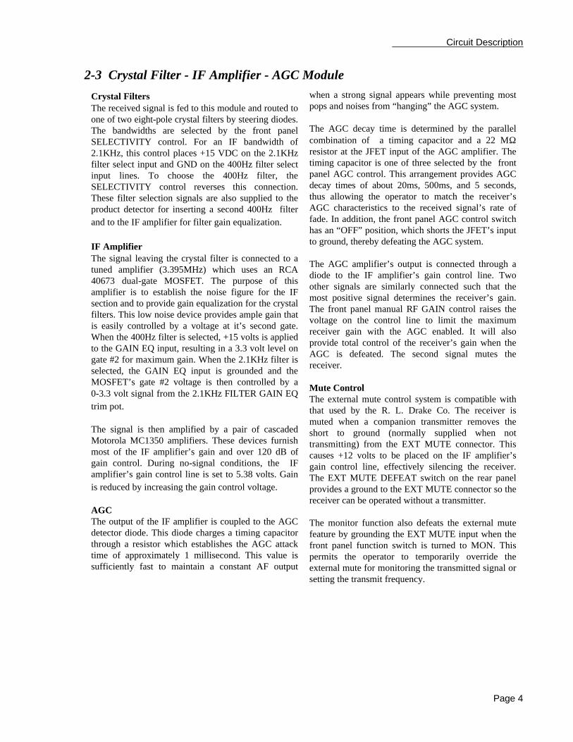
Figure 2-2 Front Panel Layout
Figure 2-3 Rear Panel Connections and Controls
AGC Control - Off/F/M/S
Signal Strength Meter
Digital Frequency Readout Main Tuning
Passband Tuning
Notch Tuning
AC Power - AF Gain ControlRF Gain Control
Selectivity Control 2.1 kHz - 400Hz
Mode SwitchMonitor - Normal - Notch Enable
AC Line Cord
Fuse 3/8 amp Slo-Blo
Antenna Input
8 Ohm Speaker Outputs
1/4" Headphone jack or
RCA Connector. Sidetone Input
External Mute Input
External Mute Defeat Switch
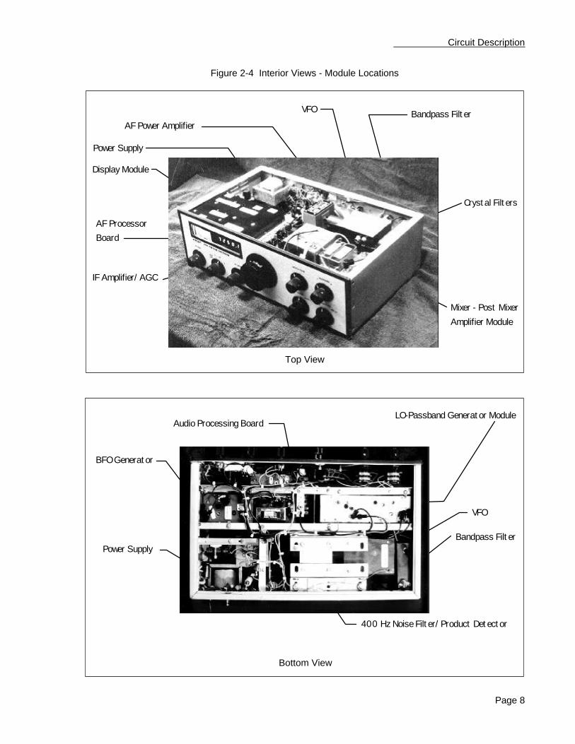
Figure 2-4 Interior Views - Module Locations
Circuit Description
Page 8
Power Supply
AF Power Amplifier
VFO Bandpass Filter
Display Module
AF ProcessorBoard
IF Amplifier/ AGC
Crystal Filters
Mixer - Post Mixer
Amplifier Module
Top View
LO-Passband Generator Module
VFO
Bandpass Filter
400 Hz Noise Filter/ Product Detector
Audio Processing Board
BFO Generator
Power Supply
Bottom View
Alignment and Calibration
3-1 Required Test Equipment
3-2 VFO
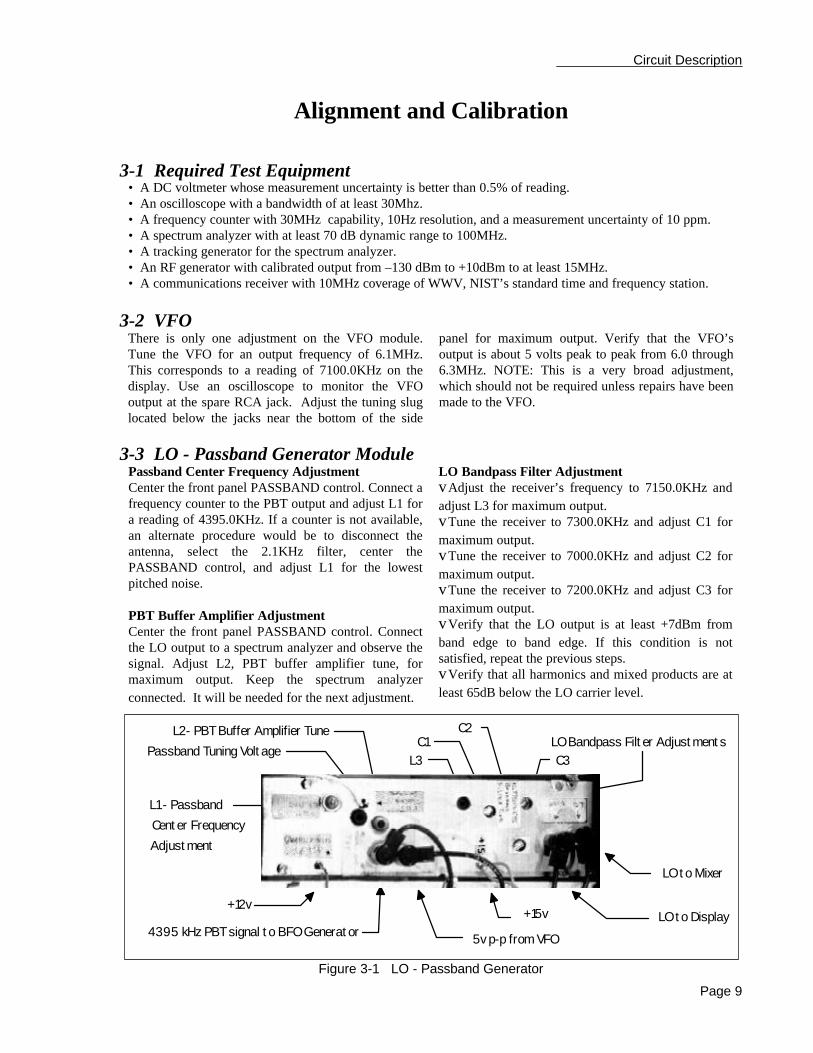
3-3 LO - Passband Generator Module
Circuit Description
Page 9
LO to Mixer
LO to Display+15v
5v p-p from VFO 4395 kHz PBT signal to BFO Generator
+12v
L1 - Passband
Center Frequency
Adjustment
L2- PBT Buffer Amplifier TuneLO Bandpass Filter Adjustments
Passband Tuning VoltageL3
C1C2
C3
Figure 3-1 LO - Passband Generator
Passband Center Frequency AdjustmentCenter the front panel PASSBAND control. Connect afrequency counter to the PBT output and adjust L1 fora reading of 4395.0KHz. If a counter is not available,an alternate procedure would be to disconnect theantenna, select the 2.1KHz filter, center thePASSBAND control, and adjust L1 for the lowestpitched noise.
PBT Buffer Amplifier AdjustmentCenter the front panel PASSBAND control. Connectthe LO output to a spectrum analyzer and observe thesignal. Adjust L2, PBT buffer amplifier tune, formaximum output. Keep the spectrum analyzerconnected. It will be needed for the next adjustment.
LO Bandpass Filter AdjustmentvAdjust the receiver’s frequency to 7150.0KHz andadjust L3 for maximum output. vTune the receiver to 7300.0KHz and adjust C1 formaximum output.vTune the receiver to 7000.0KHz and adjust C2 formaximum output.vTune the receiver to 7200.0KHz and adjust C3 formaximum output.vVerify that the LO output is at least +7dBm fromband edge to band edge. If this condition is notsatisfied, repeat the previous steps. vVerify that all harmonics and mixed products are atleast 65dB below the LO carrier level.
• A DC voltmeter whose measurement uncertainty is better than 0.5% of reading.• An oscilloscope with a bandwidth of at least 30Mhz.• A frequency counter with 30MHz capability, 10Hz resolution, and a measurement uncertainty of 10 ppm.• A spectrum analyzer with at least 70 dB dynamic range to 100MHz.• A tracking generator for the spectrum analyzer.• An RF generator with calibrated output from –130 dBm to +10dBm to at least 15MHz.• A communications receiver with 10MHz coverage of WWV, NIST’s standard time and frequency station.
There is only one adjustment on the VFO module.Tune the VFO for an output frequency of 6.1MHz.This corresponds to a reading of 7100.0KHz on thedisplay. Use an oscilloscope to monitor the VFOoutput at the spare RCA jack. Adjust the tuning sluglocated below the jacks near the bottom of the side
panel for maximum output. Verify that the VFO’soutput is about 5 volts peak to peak from 6.0 through6.3MHz. NOTE: This is a very broad adjustment,which should not be required unless repairs have beenmade to the VFO.
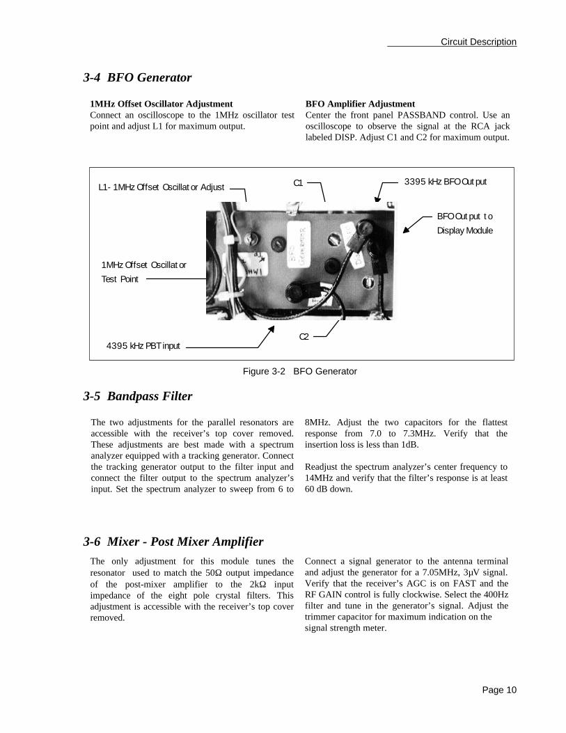
3-4 BFO Generator
1MHz Offset Oscillator AdjustmentConnect an oscilloscope to the 1MHz oscillator testpoint and adjust L1 for maximum output.
BFO Amplifier AdjustmentCenter the front panel PASSBAND control. Use anoscilloscope to observe the signal at the RCA jacklabeled DISP. Adjust C1 and C2 for maximum output.
3-5 Bandpass Filter
The two adjustments for the parallel resonators areaccessible with the receiver’s top cover removed.These adjustments are best made with a spectrumanalyzer equipped with a tracking generator. Connectthe tracking generator output to the filter input andconnect the filter output to the spectrum analyzer’sinput. Set the spectrum analyzer to sweep from 6 to
8MHz. Adjust the two capacitors for the flattestresponse from 7.0 to 7.3MHz. Verify that theinsertion loss is less than 1dB.
Readjust the spectrum analyzer’s center frequency to14MHz and verify that the filter’s response is at least60 dB down.
3-6 Mixer - Post Mixer Amplifier
The only adjustment for this module tunes theresonator used to match the 50Ω output impedanceof the post-mixer amplifier to the 2kΩ inputimpedance of the eight pole crystal filters. Thisadjustment is accessible with the receiver’s top coverremoved.
Connect a signal generator to the antenna terminaland adjust the generator for a 7.05MHz, 3µV signal.Verify that the receiver’s AGC is on FAST and theRF GAIN control is fully clockwise. Select the 400Hzfilter and tune in the generator’s signal. Adjust thetrimmer capacitor for maximum indication on thesignal strength meter.
Circuit Description
Page 10
Figure 3-2 BFO Generator
L1 - 1 MHz Offset Oscillator Adjust
1 MHz Offset Oscillator
Test Point
4395 kHz PBT input
3395 kHz BFO Output
BFO Output to
Display Module
C1
C2
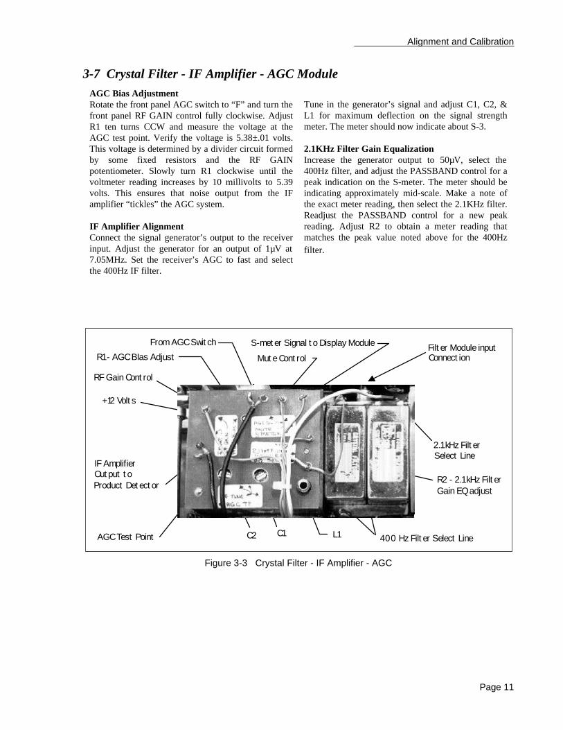
3-7 Crystal Filter - IF Amplifier - AGC Module
AGC Bias AdjustmentRotate the front panel AGC switch to “F” and turn thefront panel RF GAIN control fully clockwise. AdjustR1 ten turns CCW and measure the voltage at theAGC test point. Verify the voltage is 5.38±.01 volts.This voltage is determined by a divider circuit formedby some fixed resistors and the RF GAINpotentiometer. Slowly turn R1 clockwise until thevoltmeter reading increases by 10 millivolts to 5.39volts. This ensures that noise output from the IFamplifier “tickles” the AGC system.
IF Amplifier AlignmentConnect the signal generator’s output to the receiverinput. Adjust the generator for an output of 1µV at7.05MHz. Set the receiver’s AGC to fast and selectthe 400Hz IF filter.
Tune in the generator’s signal and adjust C1, C2, &L1 for maximum deflection on the signal strengthmeter. The meter should now indicate about S-3.
2.1KHz Filter Gain EqualizationIncrease the generator output to 50µV, select the400Hz filter, and adjust the PASSBAND control for apeak indication on the S-meter. The meter should beindicating approximately mid-scale. Make a note ofthe exact meter reading, then select the 2.1KHz filter.Readjust the PASSBAND control for a new peakreading. Adjust R2 to obtain a meter reading thatmatches the peak value noted above for the 400Hzfilter.
Alignment and Calibration
Page 11
L1C1C2AGC Test Point
IF Amplifier Output toProduct Detector
RF Gain Control
R1 - AGC BIas Adjust
From AGC Switch S-meter Signal to Display Module
Mute Control
+12 Volts
400 Hz Filter Select Line
2.1 kHz FilterSelect Line
Filter Module inputConnection
R2 - 2.1 kHz FilterGain EQ adjust
Figure 3-3 Crystal Filter - IF Amplifier - AGC
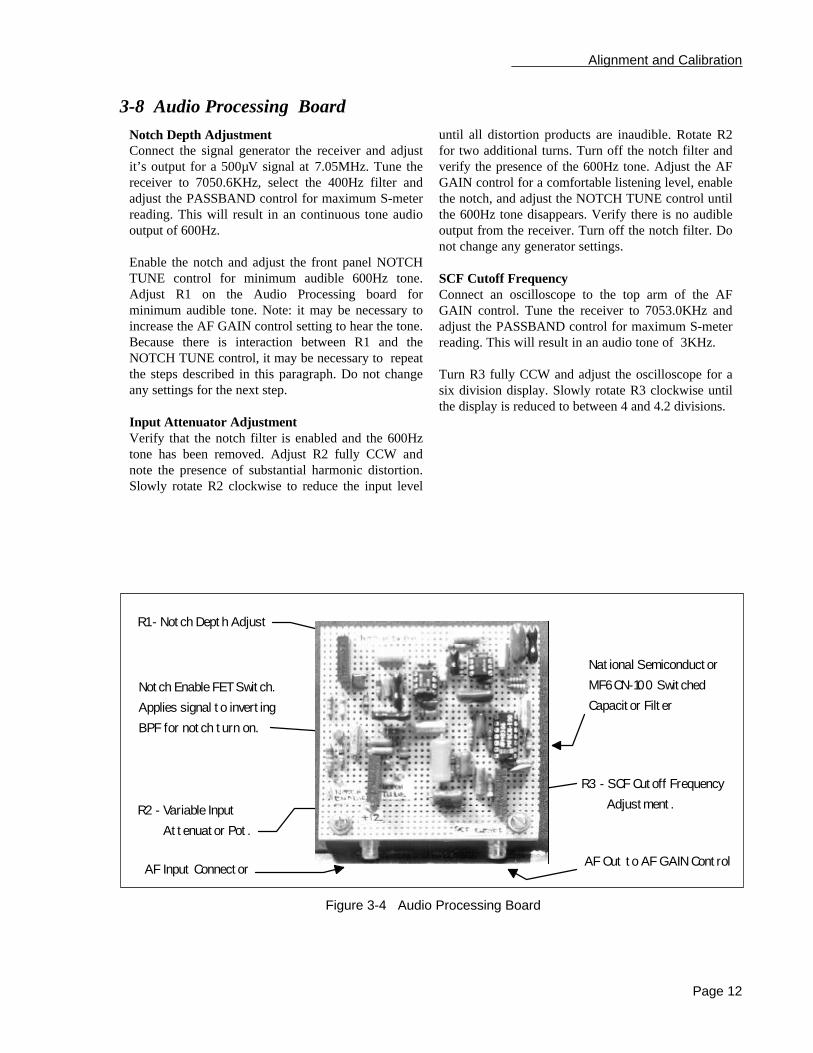
3-8 Audio Processing Board
Notch Depth AdjustmentConnect the signal generator the receiver and adjustit’s output for a 500µV signal at 7.05MHz. Tune thereceiver to 7050.6KHz, select the 400Hz filter andadjust the PASSBAND control for maximum S-meterreading. This will result in an continuous tone audiooutput of 600Hz.
Enable the notch and adjust the front panel NOTCHTUNE control for minimum audible 600Hz tone.Adjust R1 on the Audio Processing board forminimum audible tone. Note: it may be necessary toincrease the AF GAIN control setting to hear the tone.Because there is interaction between R1 and theNOTCH TUNE control, it may be necessary to repeatthe steps described in this paragraph. Do not changeany settings for the next step.
Input Attenuator AdjustmentVerify that the notch filter is enabled and the 600Hztone has been removed. Adjust R2 fully CCW andnote the presence of substantial harmonic distortion.Slowly rotate R2 clockwise to reduce the input level
until all distortion products are inaudible. Rotate R2for two additional turns. Turn off the notch filter andverify the presence of the 600Hz tone. Adjust the AFGAIN control for a comfortable listening level, enablethe notch, and adjust the NOTCH TUNE control untilthe 600Hz tone disappears. Verify there is no audibleoutput from the receiver. Turn off the notch filter. Donot change any generator settings.
SCF Cutoff FrequencyConnect an oscilloscope to the top arm of the AFGAIN control. Tune the receiver to 7053.0KHz andadjust the PASSBAND control for maximum S-meterreading. This will result in an audio tone of 3KHz.
Turn R3 fully CCW and adjust the oscilloscope for asix division display. Slowly rotate R3 clockwise untilthe display is reduced to between 4 and 4.2 divisions.
Alignment and Calibration
Page 12
R1 - Notch Depth Adjust
Notch Enable FET Switch.
Applies signal to inverting
BPF for notch turn on.
R2 - Variable Input
Attenuator Pot.
R3 - SCF Cutoff Frequency
National Semiconductor
MF6CN-100 Switched
Capacitor Filter
Adjustment.
AF Input Connector AF Out to AF GAIN Control
Figure 3-4 Audio Processing Board

3-9 Display Module
Counter Timebase CalibrationPlace the communications receiver in the AM modeand tune to WWV at 10MHz. Use a ten foot piece ofwire as an antenna and position it near the displaymodule. Adjust the antenna’s position such that thestrength of the time base signal is comparable toWWV’s. Adjust C1 such that the time base signal iszero-beat with WWV’s carrier frequency.
Counter Amplifier AdjustmentThe counter amplifier tuning is not critical andadjustments should not be required unless repairshave been made to the DISPLAY MODULE.Readjustment is required when the frequency readoutwill not display reliably from band edge to bandedge.
Tune the K9GDT receiver for a display reading of7125.0KHz. Next, tune the test communicationsreceiver to 7125KHz and pick up the signal generatedby the DISPLAY MODULE.
Note: It may be necessary to reposition the testreceiver’s antenna very close to L3 in order to pick upa good signal.
Tune L1, L2, and L3 for maximum signal strength asindicated on the test receiver’s S-meter. Verify thatthe frequency readout on the DISPLAY MODULE isstable from band edge to band edge.
S-meter AdjustmentTune the receiver to 7050.0KHz, turn the RF GAINfully clockwise, the AGC to AGC OFF and select the400Hz filter. Remove the signal generator and adjustR2 for a reading of S-1.
Reconnect the signal generator and adjust it’s outputto 30 mV at 7.05MHz. Turn the AGC switch to “F”and adjust the PASSBAND control for maximumreading on the S-meter. Adjust R1 for a full scalemeter reading of +60 dB.
Alignment and Calibration
Page 13
L1 - LO Buffer Amp Tune
LO Input (Top)
PBT Input (Bottom)
L2 - 7 MHz Amp TuneC1 - Counter Time Base Adjust
L3 - 7 MHz Amp Tune
R1 - Signal Strength Meter Full Scale Adj.
R2 - Signal Strength Meter Zero Adj.
M1 - 100 Microamperes F.S.
+5 Volts+12 Volts
Figure 3-5 Display Module