Journal of Crystal Growth - ir.nctu.edu.tw · Journal of Crystal Growth 312 (2010) 3574–3578...
5
Method for modulating the wafer bow of free-standing GaN substrates via inductively coupled plasma etching Kuei-Ming Chen a,b,n , Yen-Hsien Yeh a , Yin-Hao Wu a , Chen-Hao Chiang a , Din-Ru Yang a , Chu-Li Chao a,b , Tung-Wei Chi b , Yen-Hsang Fang b , Jenq-Dar Tsay b , Wei-I Lee a a Department of Electrophysics, National Chiao Tung University, 1001 University Road, Hsinchu 30010, Taiwan b Electronics and Optoelectronics Research Laboratories, Industrial Technology Research Institute, Hsinchu, Taiwan article info Article history: Received 26 May 2010 Received in revised form 31 August 2010 Accepted 16 September 2010 Communicated by M. Schieber Available online 24 September 2010 Keywords: A1. Etching A1. GaN substrate A3. Hydride vapor phase epitaxy B1. Nitrides B2. GaN abstract The bowing curvature of the free-standing GaN substrate significantly decreased almost linearly from 0.67 to 0.056 m 1 (i.e. the bowing radius increased from 1.5 to 17.8 m) with increase in inductively coupled plasma (ICP) etching time at the N-polar face, and eventually changed the bowing direction from convex to concave. Furthermore, the influences of the bowing curvature on the measured full width at half maximum (FWHM) of high-resolution X-ray diffraction (HRXRD) in (0 0 2) reflection were also deduced, which reduced from 176.8 to 88.8 arcsec with increase in ICP etching time. Decrease in the nonhomogeneous distribution of threading dislocations and point defects as well as V Ga –O N complex defects on removing the GaN layer from N-polar face, which removed large amount of defects, was one of the reasons that improved the bowing of the free-standing GaN substrate. Another reason was the high aspect ratio of needle-like GaN that appeared at the N-polar face after ICP etching, which released the compressive strain of the free-standing GaN substrate. By doing so, crack-free and extremely flat free-standing GaN substrates with a bowing radius of 17.8 m could be obtained. & 2010 Elsevier B.V. All rights reserved. 1. Introduction Currently, III-nitride devices are grown on different substrates, such as GaN, sapphire, Si, and SiC substrates. The performance of III-nitride devices grown on sapphire, Si, and SiC substrates is significantly limited by the structural quality of these materials as a result of heteroepitaxy [1]. The advantages of using GaN substrate for homoepitaxy are low dislocation density (at least two orders lower than other substrates) and thermal expansion match, which significantly improved the performance and wafer bow, respectively. Furthermore, vertical devices could be grown on electrically conductive GaN substrates to reduce current crowding and self-heating effects of devices. Free-standing GaN substrates have been widely used in laser diodes (LDs) [2] and high-power light emitting diodes (LEDs) [3] owing to its low dislocation density and superior thermal electrical properties. Currently, free-standing GaN substrates can be successfully obtained by growing thick GaN film hetero-epitaxially on a foreign base substrate in hydride vapor phase epitaxy (HVPE), and subsequently separating from the original substrate using laser lift-off (LLO) [4], chemical lift-off [5], and self-separation [6]. However, the free-standing GaN substrates experience a serious issue of bowing, which makes the chemical mechanical polish (CMP) processes difficult and complicated. The bowing of free- standing GaN substrates has been suggested for nonhomogeneous distribution of threading dislocations and V Ga –O N complex defects in the growth direction, especially exit large amount at the N-polar face of c-plane free-standing GaN substrates [7,8]. Normally, a 2 in. free-standing GaN substrate with the bowing radius of 0.6–1.5 m may lead to 500–200 mm height difference between the center and edge of the free-standing GaN substrate, which may even be thicker than the GaN substrate itself [9,10]. This height difference of the free-standing GaN substrates owing to bowing may totally remove the GaN layer around the edge region, but may not polish the GaN layer around the center region during the CMP processes. In this study, we used ICP-etched N-polar face of the free-standing GaN substrate to modulate the bowing curvatures and directions, and then eventually obtained an extremely flat free-standing GaN substrate. 2. Experimental procedure In the experiment, a 3-mm-thick GaN was initially grown on c-plane sapphire substrate using MOCVD as GaN template. Contents lists available at ScienceDirect journal homepage: www.elsevier.com/locate/jcrysgro Journal of Crystal Growth 0022-0248/$ - see front matter & 2010 Elsevier B.V. All rights reserved. doi:10.1016/j.jcrysgro.2010.09.044 n Corresponding author at: Department of Electrophysics, National Chiao Tung University, 1001 University Road, Hsinchu 30010, Taiwan. Tel.: + 886 3 571 2121 56151; fax: + 886 3 572 5230. E-mail address: [email protected] (K.M. Chen). Journal of Crystal Growth 312 (2010) 3574–3578
Transcript of Journal of Crystal Growth - ir.nctu.edu.tw · Journal of Crystal Growth 312 (2010) 3574–3578...
Journal of Crystal Growth 312 (2010) 3574–3578
Contents lists available at ScienceDirect
Journal of Crystal Growth
0022-02
doi:10.1
n Corr
Univers
Tel.: +8
E-m
journal homepage: www.elsevier.com/locate/jcrysgro
Method for modulating the wafer bow of free-standing GaN substrates viainductively coupled plasma etching
Kuei-Ming Chen a,b,n, Yen-Hsien Yeh a, Yin-Hao Wu a, Chen-Hao Chiang a, Din-Ru Yang a, Chu-Li Chao a,b,Tung-Wei Chi b, Yen-Hsang Fang b, Jenq-Dar Tsay b, Wei-I Lee a
a Department of Electrophysics, National Chiao Tung University, 1001 University Road, Hsinchu 30010, Taiwanb Electronics and Optoelectronics Research Laboratories, Industrial Technology Research Institute, Hsinchu, Taiwan
a r t i c l e i n f o
Article history:
Received 26 May 2010
Received in revised form
31 August 2010
Accepted 16 September 2010
Communicated by M. Schieberwidth at half maximum (FWHM) of high-resolution X-ray diffraction (HRXRD) in (0 0 2) reflection were
Available online 24 September 2010
Keywords:
A1. Etching
A1. GaN substrate
A3. Hydride vapor phase epitaxy
B1. Nitrides
B2. GaN
48/$ - see front matter & 2010 Elsevier B.V. A
016/j.jcrysgro.2010.09.044
esponding author at: Department of Electrop
ity, 1001 University Road, Hsinchu 30010, Ta
86 3 571 2121 56151; fax: +886 3 572 5230.
ail address: [email protected] (K.M
a b s t r a c t
The bowing curvature of the free-standing GaN substrate significantly decreased almost linearly from
0.67 to 0.056 m�1 (i.e. the bowing radius increased from 1.5 to 17.8 m) with increase in inductively
coupled plasma (ICP) etching time at the N-polar face, and eventually changed the bowing direction
from convex to concave. Furthermore, the influences of the bowing curvature on the measured full
also deduced, which reduced from 176.8 to 88.8 arcsec with increase in ICP etching time. Decrease in
the nonhomogeneous distribution of threading dislocations and point defects as well as VGa–ON
complex defects on removing the GaN layer from N-polar face, which removed large amount of defects,
was one of the reasons that improved the bowing of the free-standing GaN substrate. Another reason
was the high aspect ratio of needle-like GaN that appeared at the N-polar face after ICP etching, which
released the compressive strain of the free-standing GaN substrate. By doing so, crack-free and
extremely flat free-standing GaN substrates with a bowing radius of 17.8 m could be obtained.
& 2010 Elsevier B.V. All rights reserved.
1. Introduction
Currently, III-nitride devices are grown on different substrates,such as GaN, sapphire, Si, and SiC substrates. The performance ofIII-nitride devices grown on sapphire, Si, and SiC substrates issignificantly limited by the structural quality of these materials asa result of heteroepitaxy [1]. The advantages of using GaNsubstrate for homoepitaxy are low dislocation density (at leasttwo orders lower than other substrates) and thermal expansionmatch, which significantly improved the performance and waferbow, respectively. Furthermore, vertical devices could be grownon electrically conductive GaN substrates to reduce currentcrowding and self-heating effects of devices. Free-standing GaNsubstrates have been widely used in laser diodes (LDs) [2] andhigh-power light emitting diodes (LEDs) [3] owing to its lowdislocation density and superior thermal electrical properties.Currently, free-standing GaN substrates can be successfullyobtained by growing thick GaN film hetero-epitaxially on aforeign base substrate in hydride vapor phase epitaxy (HVPE), andsubsequently separating from the original substrate using laser
ll rights reserved.
hysics, National Chiao Tung
iwan.
. Chen).
lift-off (LLO) [4], chemical lift-off [5], and self-separation [6].However, the free-standing GaN substrates experience a seriousissue of bowing, which makes the chemical mechanical polish(CMP) processes difficult and complicated. The bowing of free-standing GaN substrates has been suggested for nonhomogeneousdistribution of threading dislocations and VGa–ON complexdefects in the growth direction, especially exit large amount atthe N-polar face of c-plane free-standing GaN substrates [7,8].Normally, a 2 in. free-standing GaN substrate with the bowingradius of 0.6–1.5 m may lead to 500–200 mm height differencebetween the center and edge of the free-standing GaN substrate,which may even be thicker than the GaN substrate itself [9,10].This height difference of the free-standing GaN substrates owingto bowing may totally remove the GaN layer around the edgeregion, but may not polish the GaN layer around the center regionduring the CMP processes. In this study, we used ICP-etchedN-polar face of the free-standing GaN substrate to modulate thebowing curvatures and directions, and then eventually obtainedan extremely flat free-standing GaN substrate.
2. Experimental procedure
In the experiment, a 3-mm-thick GaN was initially grown onc-plane sapphire substrate using MOCVD as GaN template.
K.M. Chen et al. / Journal of Crystal Growth 312 (2010) 3574–3578 3575
Subsequently, we used HVPE to grow 230-mm-thick GaN templateby employing temperature ramping techniques developed in ourearlier study [11]. During the growth of GaN in the HVPE reactor,NH3 and GaCl generated from liquid gallium and HCl gas at 850 1Cwere used as the V and III group sources, respectively. Thepressure was maintained at 700 Torr, and a mixture of H2 and N2
was applied as the carrier gas. Subsequently, the thick GaN filmwas separated from the sapphire substrate by LLO with a 355 nmNd:YAG laser to make 230-mm-thick crack-free free-standing GaNsubstrate. Subsequently, the N-polar face of the free-standing GaNsubstrate was etched by ICP with increase in etching time from 7,21, 35, 49, 63 to 77 min to examine the bowing phenomenon ofthe free-standing GaN substrate. In the series of ICP etchingexperiments, Cl2 gas of 15 and Ar gas of 5 sccm were constantlytransported into the chamber, while the coil power and platenpower were fixed at 400 and 100 W, respectively.
The bowing radius of the free-standing GaN substrate wasmeasured at the Ga-polar face using a spherometer. HRXRD wasalso applied at the Ga-polar face of the free-standing GaNsubstrate to measure the FWHM variation. The (0 0 2) diffractionpeaks in X-ray o-scan were identified using a Bede D1 systemwith the slit width of 0.5 mm. Surface morphology of the N-polarface of the free-standing GaN substrate after ICP etching wasobserved by scanning electronic microscope (SEM). Opticalmeasurements of room-temperature photoluminescence (PL)
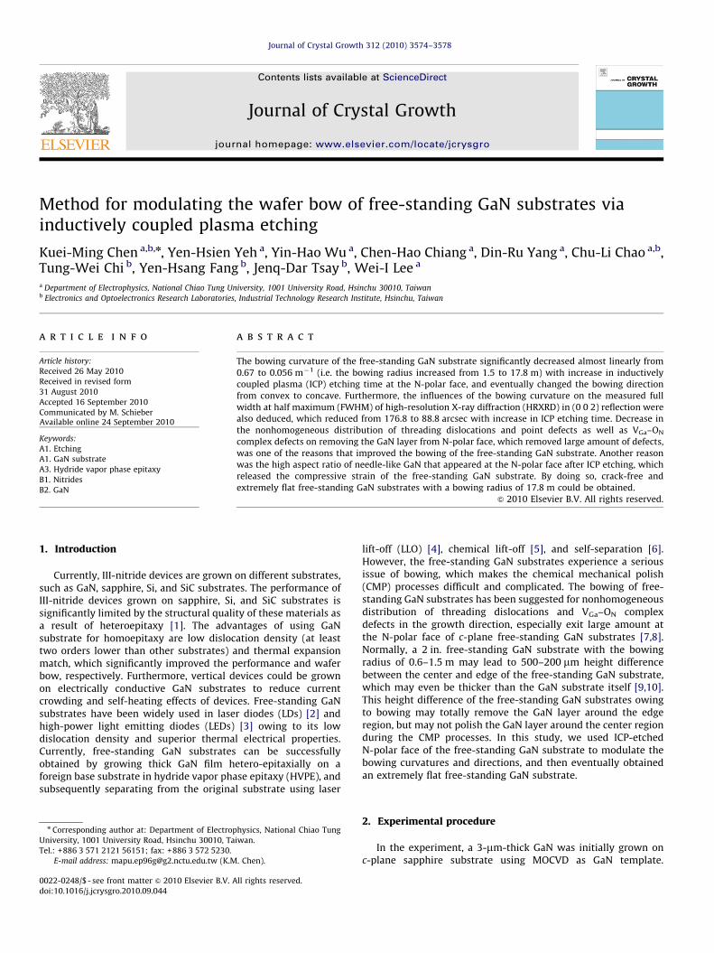
Fig. 1. Bowing directions and curvatures of the free-standing GaN substrate with
increase in ICP etching time at the N-polar face.
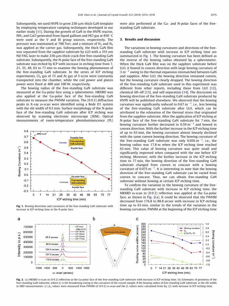
Fig. 2. (a) HRXRD o-scan in (0 0 2) reflection at the Ga-polar face of the free-standing
free-standing GaN substrate, where br is the broadening owing to the curvature of the c
in XRD measurements. (c) bm values were measured from FWHM of (0 0 2) o-scan an
were also performed at the Ga- and N-polar faces of the free-standing GaN substrate.
3. Results and discussion
The variations in bowing curvatures and directions of the free-standing GaN substrate with increase in ICP etching time aresummarized in Fig. 1. The bowing curvature has been defined asthe inverse of the bowing radius obtained by a spherometer.When the thick GaN film was on the sapphire substrate beforeLLO, it bowed in convex direction with large bowing curvature of3 m�1 owing to the thermal expansion mismatched between GaNand sapphire. After LLO, the bowing direction remained convex,but the bowing curvature clearly dropped. The bowing directionof the free-standing GaN substrate used in this experiment wasdifferent from other reports, including those from LLO [12],chemical lift-off [13], and self-separation [14]. The discussion onbowing direction of the free-standing GaN substrate produced byHVPE will be published elsewhere. We observed that the bowingcurvature was significantly reduced to 0.67 m�1, i.e., less bowingof the free-standing GaN substrate after LLO, which can beattributed to the relaxation of the thermal stress that originatedfrom the sapphire substrate. After the application of ICP etching atN-polar face of the free-standing GaN substrate for 7 min, thebowing curvature further decreased to 0.59 m�1 and bowed inconvex direction. With the further increase in the ICP etching timeof up to 63 min, the bowing curvature almost linearly declinedwith the same convex bowing direction. The bowing curvature ofthe free-standing GaN substrate was only 0.056 m�1, i.e., thebowing radius was 17.8 m when the ICP etching time reached63 min. This value of bowing curvature was quite small andsignificantly improved when compared with the one before ICPetching. Moreover, with the further increase in the ICP etchingtime to 77 min, the bowing direction of the free-standing GaNsubstrate changed from convex to concave with a bowingcurvature of 0.075 m�1. It is interesting to note that the bowingdirection of the free-standing GaN substrate can be varied fromconvex to concave. Thus, we can obtain free-standing GaNsubstrate without bowing at certain ICP etching time.
To confirm the variation in the bowing curvature of the free-standing GaN substrate with increase in ICP etching time, theHRXRD o-scan in (0 0 2) reflection was applied at the Ga-polarface, as shown in Fig. 2(a). It could be observed that the FWHMdecreased from 176.8 to 88.8 arcsec with increase in ICP etchingtime up to 63 min, similar to the trends of the variation in thebowing curvature. FWHM at the beginning of the ICP etching time
GaN substrate with increase in ICP etching time. (b) Schematic of geometry of the
rystal sample, R the bowing radius of free-standing GaN substrate, w the slit width
d the br values were calculated from Eq. (2) with increase in ICP etching time.
K.M. Chen et al. / Journal of Crystal Growth 312 (2010) 3574–35783576
for 7 and 21 min was not measured here. Furthermore, the FWHMslightly increased from 88.8 to 95.8 arcsec, along with the bowingcurvature increasing from 0.056 to 0.075 m�1 as the ICP etchingtime increased from 63 to 77 min. The reports indicated that themeasured FWHM of (0 0 2) symmetric XRD o-scan was related toseveral components, as shown in Eq. (1) presented in Appendix A[15,16]. As there was no variation in the other components,except the bowing curvature under the ICP etching at the N-polarface, we concluded that the decrease in FWHM in XRD measure-ments was owing to the decrease in the bowing curvature.Furthermore, we intended to distinguish the effects of br from bm.The geometry of free-standing GaN substrate is presented inFig. 2(b). From the schematic, the formula of br could be derivedfrom the trigonometric function, and can be given as
cosðbrÞ ¼ ðR2þR2�w2Þ=ð2RRÞ ð2Þ
The br values calculated from Eq. (2) are summarized inTable 1 and Fig. 2(c), which show similar trends and decrease invalues with bm and bowing curvature under increasing ICPetching time. This indicates that the influence of bowingcurvature of the free-standing GaN substrate is obvious andserious, and the effects of the bowing curvature on the measuredFWHM can simply be calculated using Eq. (2).
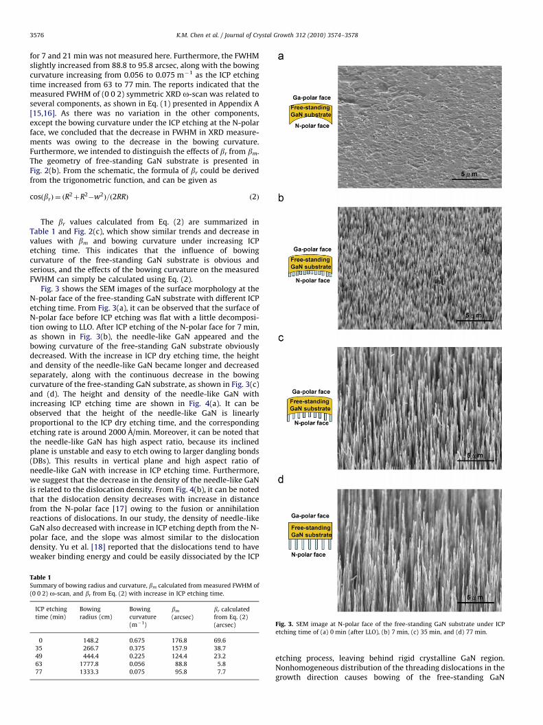
Fig. 3 shows the SEM images of the surface morphology at theN-polar face of the free-standing GaN substrate with different ICPetching time. From Fig. 3(a), it can be observed that the surface ofN-polar face before ICP etching was flat with a little decomposi-tion owing to LLO. After ICP etching of the N-polar face for 7 min,as shown in Fig. 3(b), the needle-like GaN appeared and thebowing curvature of the free-standing GaN substrate obviouslydecreased. With the increase in ICP dry etching time, the heightand density of the needle-like GaN became longer and decreasedseparately, along with the continuous decrease in the bowingcurvature of the free-standing GaN substrate, as shown in Fig. 3(c)and (d). The height and density of the needle-like GaN withincreasing ICP etching time are shown in Fig. 4(a). It can beobserved that the height of the needle-like GaN is linearlyproportional to the ICP dry etching time, and the correspondingetching rate is around 2000 A/min. Moreover, it can be noted thatthe needle-like GaN has high aspect ratio, because its inclinedplane is unstable and easy to etch owing to larger dangling bonds(DBs). This results in vertical plane and high aspect ratio ofneedle-like GaN with increase in ICP etching time. Furthermore,we suggest that the decrease in the density of the needle-like GaNis related to the dislocation density. From Fig. 4(b), it can be notedthat the dislocation density decreases with increase in distancefrom the N-polar face [17] owing to the fusion or annihilationreactions of dislocations. In our study, the density of needle-likeGaN also decreased with increase in ICP etching depth from the N-polar face, and the slope was almost similar to the dislocationdensity. Yu et al. [18] reported that the dislocations tend to haveweaker binding energy and could be easily dissociated by the ICP
Table 1
Summary of bowing radius and curvature, bm calculated from measured FWHM of
(0 0 2) o-scan, and br from Eq. (2) with increase in ICP etching time.
ICP etching
time (min)
Bowing
radius (cm)
Bowing
curvature
(m�1)
bm
(arcsec)
br calculated
from Eq. (2)
(arcsec)
0 148.2 0.675 176.8 69.6
35 266.7 0.375 157.9 38.7
49 444.4 0.225 124.4 23.2
63 1777.8 0.056 88.8 5.8
77 1333.3 0.075 95.8 7.7
Fig. 3. SEM image at N-polar face of the free-standing GaN substrate under ICP
etching time of (a) 0 min (after LLO), (b) 7 min, (c) 35 min, and (d) 77 min.
etching process, leaving behind rigid crystalline GaN region.Nonhomogeneous distribution of the threading dislocations in thegrowth direction causes bowing of the free-standing GaN
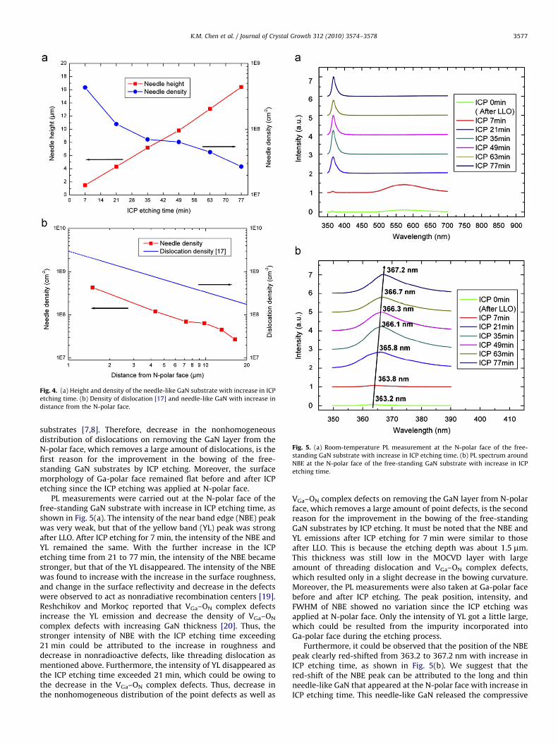
Fig. 4. (a) Height and density of the needle-like GaN substrate with increase in ICP
etching time. (b) Density of dislocation [17] and needle-like GaN with increase in
distance from the N-polar face.
Fig. 5. (a) Room-temperature PL measurement at the N-polar face of the free-
standing GaN substrate with increase in ICP etching time. (b) PL spectrum around
NBE at the N-polar face of the free-standing GaN substrate with increase in ICP
etching time.
K.M. Chen et al. / Journal of Crystal Growth 312 (2010) 3574–3578 3577
substrates [7,8]. Therefore, decrease in the nonhomogeneousdistribution of dislocations on removing the GaN layer from theN-polar face, which removes a large amount of dislocations, is thefirst reason for the improvement in the bowing of the free-standing GaN substrates by ICP etching. Moreover, the surfacemorphology of Ga-polar face remained flat before and after ICPetching since the ICP etching was applied at N-polar face.
PL measurements were carried out at the N-polar face of thefree-standing GaN substrate with increase in ICP etching time, asshown in Fig. 5(a). The intensity of the near band edge (NBE) peakwas very weak, but that of the yellow band (YL) peak was strongafter LLO. After ICP etching for 7 min, the intensity of the NBE andYL remained the same. With the further increase in the ICPetching time from 21 to 77 min, the intensity of the NBE becamestronger, but that of the YL disappeared. The intensity of the NBEwas found to increase with the increase in the surface roughness,and change in the surface reflectivity and decrease in the defectswere observed to act as nonradiative recombination centers [19].Reshchikov and Morkoc- reported that VGa–ON complex defectsincrease the YL emission and decrease the density of VGa–ON
complex defects with increasing GaN thickness [20]. Thus, thestronger intensity of NBE with the ICP etching time exceeding21 min could be attributed to the increase in roughness anddecrease in nonradioactive defects, like threading dislocation asmentioned above. Furthermore, the intensity of YL disappeared asthe ICP etching time exceeded 21 min, which could be owing tothe decrease in the VGa–ON complex defects. Thus, decrease inthe nonhomogeneous distribution of the point defects as well as
VGa–ON complex defects on removing the GaN layer from N-polarface, which removes a large amount of point defects, is the secondreason for the improvement in the bowing of the free-standingGaN substrates by ICP etching. It must be noted that the NBE andYL emissions after ICP etching for 7 min were similar to thoseafter LLO. This is because the etching depth was about 1.5 mm.This thickness was still low in the MOCVD layer with largeamount of threading dislocation and VGa–ON complex defects,which resulted only in a slight decrease in the bowing curvature.Moreover, the PL measurements were also taken at Ga-polar facebefore and after ICP etching. The peak position, intensity, andFWHM of NBE showed no variation since the ICP etching wasapplied at N-polar face. Only the intensity of YL got a little large,which could be resulted from the impurity incorporated intoGa-polar face during the etching process.
Furthermore, it could be observed that the position of the NBEpeak clearly red-shifted from 363.2 to 367.2 nm with increase inICP etching time, as shown in Fig. 5(b). We suggest that thered-shift of the NBE peak can be attributed to the long and thinneedle-like GaN that appeared at the N-polar face with increase inICP etching time. This needle-like GaN released the compressive
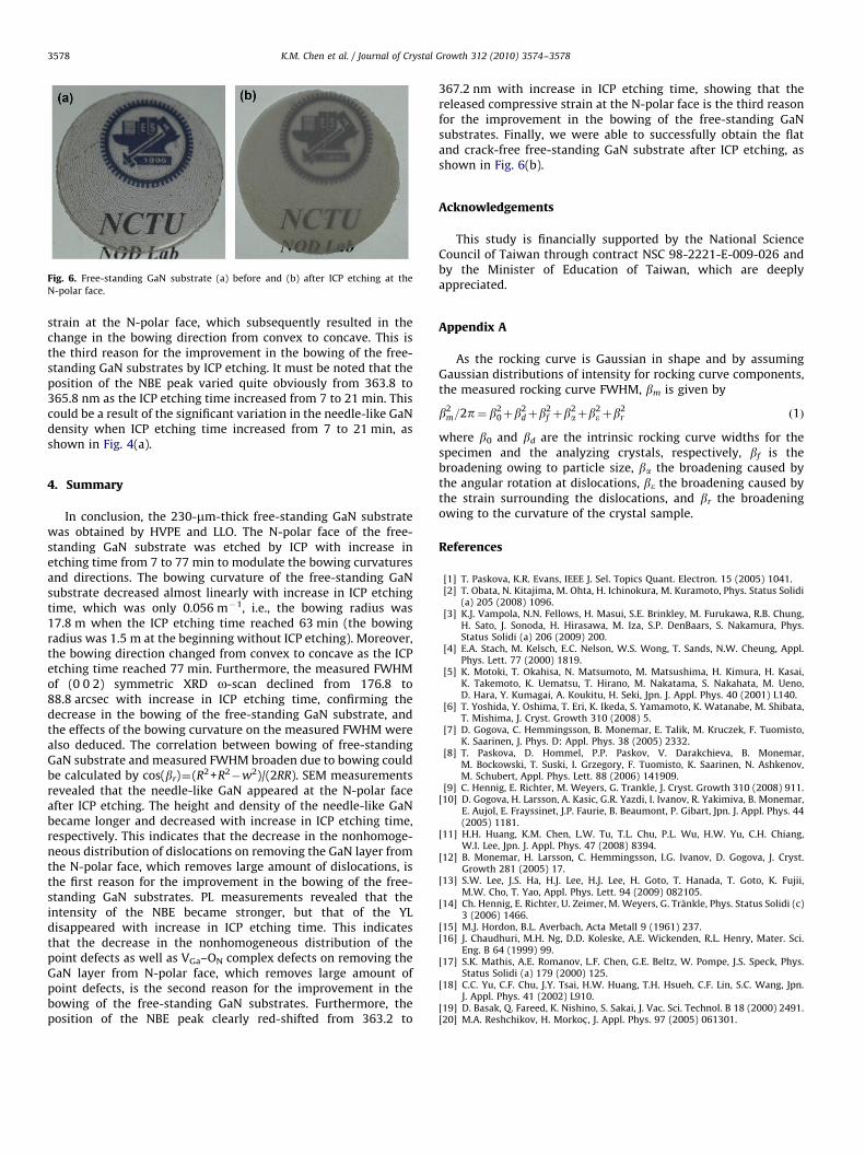
Fig. 6. Free-standing GaN substrate (a) before and (b) after ICP etching at the
N-polar face.
K.M. Chen et al. / Journal of Crystal Growth 312 (2010) 3574–35783578
strain at the N-polar face, which subsequently resulted in thechange in the bowing direction from convex to concave. This isthe third reason for the improvement in the bowing of the free-standing GaN substrates by ICP etching. It must be noted that theposition of the NBE peak varied quite obviously from 363.8 to365.8 nm as the ICP etching time increased from 7 to 21 min. Thiscould be a result of the significant variation in the needle-like GaNdensity when ICP etching time increased from 7 to 21 min, asshown in Fig. 4(a).
4. Summary
In conclusion, the 230-mm-thick free-standing GaN substratewas obtained by HVPE and LLO. The N-polar face of the free-standing GaN substrate was etched by ICP with increase inetching time from 7 to 77 min to modulate the bowing curvaturesand directions. The bowing curvature of the free-standing GaNsubstrate decreased almost linearly with increase in ICP etchingtime, which was only 0.056 m�1, i.e., the bowing radius was17.8 m when the ICP etching time reached 63 min (the bowingradius was 1.5 m at the beginning without ICP etching). Moreover,the bowing direction changed from convex to concave as the ICPetching time reached 77 min. Furthermore, the measured FWHMof (0 0 2) symmetric XRD o-scan declined from 176.8 to88.8 arcsec with increase in ICP etching time, confirming thedecrease in the bowing of the free-standing GaN substrate, andthe effects of the bowing curvature on the measured FWHM werealso deduced. The correlation between bowing of free-standingGaN substrate and measured FWHM broaden due to bowing couldbe calculated by cos(br)¼(R2+R2
�w2)/(2RR). SEM measurementsrevealed that the needle-like GaN appeared at the N-polar faceafter ICP etching. The height and density of the needle-like GaNbecame longer and decreased with increase in ICP etching time,respectively. This indicates that the decrease in the nonhomoge-neous distribution of dislocations on removing the GaN layer fromthe N-polar face, which removes large amount of dislocations, isthe first reason for the improvement in the bowing of the free-standing GaN substrates. PL measurements revealed that theintensity of the NBE became stronger, but that of the YLdisappeared with increase in ICP etching time. This indicatesthat the decrease in the nonhomogeneous distribution of thepoint defects as well as VGa–ON complex defects on removing theGaN layer from N-polar face, which removes large amount ofpoint defects, is the second reason for the improvement in thebowing of the free-standing GaN substrates. Furthermore, theposition of the NBE peak clearly red-shifted from 363.2 to
367.2 nm with increase in ICP etching time, showing that thereleased compressive strain at the N-polar face is the third reasonfor the improvement in the bowing of the free-standing GaNsubstrates. Finally, we were able to successfully obtain the flatand crack-free free-standing GaN substrate after ICP etching, asshown in Fig. 6(b).
Acknowledgements
This study is financially supported by the National ScienceCouncil of Taiwan through contract NSC 98-2221-E-009-026 andby the Minister of Education of Taiwan, which are deeplyappreciated.
Appendix A
As the rocking curve is Gaussian in shape and by assumingGaussian distributions of intensity for rocking curve components,the measured rocking curve FWHM, bm is given by
b2m=2p¼ b2
0þb2dþb
2f þb
2aþb
2e þb
2r ð1Þ
where b0 and bd are the intrinsic rocking curve widths for thespecimen and the analyzing crystals, respectively, bf is thebroadening owing to particle size, ba the broadening caused bythe angular rotation at dislocations, be the broadening caused bythe strain surrounding the dislocations, and br the broadeningowing to the curvature of the crystal sample.
References
[1] T. Paskova, K.R. Evans, IEEE J. Sel. Topics Quant. Electron. 15 (2005) 1041.[2] T. Obata, N. Kitajima, M. Ohta, H. Ichinokura, M. Kuramoto, Phys. Status Solidi
(a) 205 (2008) 1096.[3] K.J. Vampola, N.N. Fellows, H. Masui, S.E. Brinkley, M. Furukawa, R.B. Chung,
H. Sato, J. Sonoda, H. Hirasawa, M. Iza, S.P. DenBaars, S. Nakamura, Phys.Status Solidi (a) 206 (2009) 200.
[4] E.A. Stach, M. Kelsch, E.C. Nelson, W.S. Wong, T. Sands, N.W. Cheung, Appl.Phys. Lett. 77 (2000) 1819.
[5] K. Motoki, T. Okahisa, N. Matsumoto, M. Matsushima, H. Kimura, H. Kasai,K. Takemoto, K. Uematsu, T. Hirano, M. Nakatama, S. Nakahata, M. Ueno,D. Hara, Y. Kumagai, A. Koukitu, H. Seki, Jpn. J. Appl. Phys. 40 (2001) L140.
[6] T. Yoshida, Y. Oshima, T. Eri, K. Ikeda, S. Yamamoto, K. Watanabe, M. Shibata,T. Mishima, J. Cryst. Growth 310 (2008) 5.
[7] D. Gogova, C. Hemmingsson, B. Monemar, E. Talik, M. Kruczek, F. Tuomisto,K. Saarinen, J. Phys. D: Appl. Phys. 38 (2005) 2332.
[8] T. Paskova, D. Hommel, P.P. Paskov, V. Darakchieva, B. Monemar,M. Bockowski, T. Suski, I. Grzegory, F. Tuomisto, K. Saarinen, N. Ashkenov,M. Schubert, Appl. Phys. Lett. 88 (2006) 141909.
[9] C. Hennig, E. Richter, M. Weyers, G. Trankle, J. Cryst. Growth 310 (2008) 911.[10] D. Gogova, H. Larsson, A. Kasic, G.R. Yazdi, I. Ivanov, R. Yakimiva, B. Monemar,
E. Aujol, E. Frayssinet, J.P. Faurie, B. Beaumont, P. Gibart, Jpn. J. Appl. Phys. 44(2005) 1181.
[11] H.H. Huang, K.M. Chen, L.W. Tu, T.L. Chu, P.L. Wu, H.W. Yu, C.H. Chiang,W.I. Lee, Jpn. J. Appl. Phys. 47 (2008) 8394.
[12] B. Monemar, H. Larsson, C. Hemmingsson, I.G. Ivanov, D. Gogova, J. Cryst.Growth 281 (2005) 17.
[13] S.W. Lee, J.S. Ha, H.J. Lee, H.J. Lee, H. Goto, T. Hanada, T. Goto, K. Fujii,M.W. Cho, T. Yao, Appl. Phys. Lett. 94 (2009) 082105.
[14] Ch. Hennig, E. Richter, U. Zeimer, M. Weyers, G. Trankle, Phys. Status Solidi (c)3 (2006) 1466.
[15] M.J. Hordon, B.L. Averbach, Acta Metall 9 (1961) 237.[16] J. Chaudhuri, M.H. Ng, D.D. Koleske, A.E. Wickenden, R.L. Henry, Mater. Sci.
Eng. B 64 (1999) 99.[17] S.K. Mathis, A.E. Romanov, L.F. Chen, G.E. Beltz, W. Pompe, J.S. Speck, Phys.
Status Solidi (a) 179 (2000) 125.[18] C.C. Yu, C.F. Chu, J.Y. Tsai, H.W. Huang, T.H. Hsueh, C.F. Lin, S.C. Wang, Jpn.
J. Appl. Phys. 41 (2002) L910.[19] D. Basak, Q. Fareed, K. Nishino, S. Sakai, J. Vac. Sci. Technol. B 18 (2000) 2491.[20] M.A. Reshchikov, H. Morkoc- , J. Appl. Phys. 97 (2005) 061301.