
Journal of Alloys and Compounds - Department of...
7
Journal of Alloys and Compounds 509 (2011) 3319–3325 Contents lists available at ScienceDirect Journal of Alloys and Compounds journal homepage: www.elsevier.com/locate/jallcom Microstructure, kinetic analysis and hardness of Sn–Ag–Cu–1 wt% nano-ZrO 2 composite solder on OSP-Cu pads Asit Kumar Gain a , Tama Fouzder a , Y.C. Chan a,∗ , Winco K.C. Yung b a Department of Electronic Engineering, City University of Hong Kong, Tat Chee Avenue, Kowloon Tong, Hong Kong b Department of Industrial and Systems Engineering, The Hong Kong Polytechnic University, Hung Hom, Kowloon, Hong Kong article info Article history: Received 27 September 2010 Received in revised form 5 December 2010 Accepted 7 December 2010 Available online 14 December 2010 Keywords: Nano doping Microstructure Kinetics analysis Hardness abstract Nano-sized, nonreacting, noncoarsening ZrO 2 particle-reinforced Sn–Ag–Cu composite solders were prepared by mechanically dispersing ZrO 2 nano-particles into Sn–Ag–Cu solder and the interfacial mor- phology between the solder and organic solderability preservative (OSP)-Cu pads were characterized metallographically. At their interfaces, island-shaped Cu 6 Sn 5 and Cu 3 Sn intermetallic compound (IMC) layers were found in solder joints with and without the ZrO 2 particles and the IMC layer thickness was substantially increased with reaction time and temperature. In the solder ball region, needle-shaped Ag 3 Sn and spherically-shaped Cu 6 Sn 5 IMC particles were found to be uniformly distributed in the –Sn matrix. However, after the addition of ZrO 2 nano-particles, Ag 3 Sn and Cu 6 Sn 5 IMC particles appeared with a fine microstructure and retarded the growth rate of the IMC layers at their interfaces. From a kinetic analysis, the calculated activation energies for the total (Cu 6 Sn 5 + Cu 3 Sn) IMC layers for Sn–Ag–Cu and Sn–Ag–Cu–1 wt% ZrO 2 composite solder joints on OSP-Cu pads were about 53.2 and 59.5 kJ/mol, respectively. In addition, solder joints containing ZrO 2 nano-particles displayed higher hardness due to the uniform distribution of ZrO 2 nano-particles as well as the refined IMC particles. The hardness values of the plain Sn–Ag–Cu solder joint and solder joints containing 1 wt% of ZrO 2 nano-particles after 5 min reaction at 250 ◦ C were about 15.0 Hv and 17.1 Hv, respectively. On the other hand, their hardness values after 30 min reaction were about 13.7 Hv and 15.5 Hv, respectively. © 2010 Elsevier B.V. All rights reserved. 1. Introduction Due to the inherent toxicity of lead (Pb) and Pb-containing alloys, environmental regulations and health concerns around the world have been targeted to eliminate the usage of Pb-bearing sol- ders in the electronic packaging industry [1–3]. This has prompted a search for “lead-free” solders and more attention in the research activities in this field. Up to now, several types of binary and ternary Sn-based lead-free solders such as Sn–Ag, Sn–Cu, Sn–Au, Sn–Ag–Cu and Sn–Zn have been developed and applied in the electronic pack- aging industry [4–6]. Among the various types of lead-free solders, with a combination of process attributes like a modest melting temperature and reasonable solderability, comparable electrical performance and good mechanical properties, Sn–Ag–Cu solder has been proposed as one of the most promising substitutes for conventional Sn–Pb solder [7,8]. Moreover, with the advancement of micro-/nanosystems technology through the years, microelec- tronic components have evolved to become smaller, lighter and ∗ Corresponding author. Tel.: +852 27887130; fax: +852 2788 7579. E-mail address: [email protected] (Y.C. Chan). more functional. Therefore, conventional solder technology can on longer guarantee the solder joint reliability of electronic com- ponents. In general, the reliability of the solder joints is mainly dependent on an interfacial IMC layer, the difference in coefficients of thermal expansion, the yield strength, elastic modulus, shear strength, fatigue and creep behavior [9]. Studies have revealed that the additions of nano-sized, nonreacting, noncoarsening particles to a solder matrix provide a marked improvement in microstruc- tural modification and mechanical properties [10]. Shen and Chan [11] successfully prepared Sn–9Zn–1 wt% ZrO 2 composite solder by mechanical mixing method, and this composite solder improved the shear strength, suppressed the growth of Sn–Ni IMCs and refined the microstructure. Noh et al. [12] used Ce particles as reinforcements for a conventional Sn–Ag solder and reported sig- nificant enhancement in wettability and mechanical properties. Tai et al. [13] prepared 20 vol% Cu 6 Sn 5 reinforced Sn–3.5Ag composite solder by an in situ method and the composite solder joint exhib- ited a better steady-state creep strain rate, less thermomechanical fatigue damage and higher shear strengths after different num- bers of thermomechanical fatigue cycles as compared to a plain Sn–3.5Ag solder joint. Xiao et al. [14] reported that rare earth rein- forced Sn–Ag–Cu composite solder suppressed the formation of 0925-8388/$ – see front matter © 2010 Elsevier B.V. All rights reserved. doi:10.1016/j.jallcom.2010.12.048
-
Upload
nguyenthuan -
Category
Documents
-
view
213 -
download
0
Transcript of Journal of Alloys and Compounds - Department of...

Mc
Aa
b
a
ARRAA
KNMKH
1
awdaaSaawtphcot
0d
Journal of Alloys and Compounds 509 (2011) 3319–3325
Contents lists available at ScienceDirect
Journal of Alloys and Compounds
journa l homepage: www.e lsev ier .com/ locate / ja l l com
icrostructure, kinetic analysis and hardness of Sn–Ag–Cu–1 wt% nano-ZrO2
omposite solder on OSP-Cu pads
sit Kumar Gaina, Tama Fouzdera, Y.C. Chana,∗, Winco K.C. Yungb
Department of Electronic Engineering, City University of Hong Kong, Tat Chee Avenue, Kowloon Tong, Hong KongDepartment of Industrial and Systems Engineering, The Hong Kong Polytechnic University, Hung Hom, Kowloon, Hong Kong
r t i c l e i n f o
rticle history:eceived 27 September 2010eceived in revised form 5 December 2010ccepted 7 December 2010vailable online 14 December 2010
eywords:ano dopingicrostructure
inetics analysis
a b s t r a c t
Nano-sized, nonreacting, noncoarsening ZrO2 particle-reinforced Sn–Ag–Cu composite solders wereprepared by mechanically dispersing ZrO2 nano-particles into Sn–Ag–Cu solder and the interfacial mor-phology between the solder and organic solderability preservative (OSP)-Cu pads were characterizedmetallographically. At their interfaces, island-shaped Cu6Sn5 and Cu3Sn intermetallic compound (IMC)layers were found in solder joints with and without the ZrO2 particles and the IMC layer thickness wassubstantially increased with reaction time and temperature. In the solder ball region, needle-shapedAg3Sn and spherically-shaped Cu6Sn5 IMC particles were found to be uniformly distributed in the �–Snmatrix. However, after the addition of ZrO2 nano-particles, Ag3Sn and Cu6Sn5 IMC particles appearedwith a fine microstructure and retarded the growth rate of the IMC layers at their interfaces. From a
ardness kinetic analysis, the calculated activation energies for the total (Cu6Sn5 + Cu3Sn) IMC layers for Sn–Ag–Cuand Sn–Ag–Cu–1 wt% ZrO2 composite solder joints on OSP-Cu pads were about 53.2 and 59.5 kJ/mol,respectively. In addition, solder joints containing ZrO2 nano-particles displayed higher hardness due tothe uniform distribution of ZrO2 nano-particles as well as the refined IMC particles. The hardness valuesof the plain Sn–Ag–Cu solder joint and solder joints containing 1 wt% of ZrO2 nano-particles after 5 minreaction at 250 ◦C were about 15.0 Hv and 17.1 Hv, respectively. On the other hand, their hardness valuesafter 30 min reaction were about 13.7 Hv and 15.5 Hv, respectively.
. Introduction
Due to the inherent toxicity of lead (Pb) and Pb-containinglloys, environmental regulations and health concerns around theorld have been targeted to eliminate the usage of Pb-bearing sol-ers in the electronic packaging industry [1–3]. This has promptedsearch for “lead-free” solders and more attention in the researchctivities in this field. Up to now, several types of binary and ternaryn-based lead-free solders such as Sn–Ag, Sn–Cu, Sn–Au, Sn–Ag–Cund Sn–Zn have been developed and applied in the electronic pack-ging industry [4–6]. Among the various types of lead-free solders,ith a combination of process attributes like a modest melting
emperature and reasonable solderability, comparable electricalerformance and good mechanical properties, Sn–Ag–Cu solder
as been proposed as one of the most promising substitutes foronventional Sn–Pb solder [7,8]. Moreover, with the advancementf micro-/nanosystems technology through the years, microelec-ronic components have evolved to become smaller, lighter and∗ Corresponding author. Tel.: +852 27887130; fax: +852 2788 7579.E-mail address: [email protected] (Y.C. Chan).
925-8388/$ – see front matter © 2010 Elsevier B.V. All rights reserved.oi:10.1016/j.jallcom.2010.12.048
© 2010 Elsevier B.V. All rights reserved.
more functional. Therefore, conventional solder technology canon longer guarantee the solder joint reliability of electronic com-ponents. In general, the reliability of the solder joints is mainlydependent on an interfacial IMC layer, the difference in coefficientsof thermal expansion, the yield strength, elastic modulus, shearstrength, fatigue and creep behavior [9]. Studies have revealed thatthe additions of nano-sized, nonreacting, noncoarsening particlesto a solder matrix provide a marked improvement in microstruc-tural modification and mechanical properties [10]. Shen and Chan[11] successfully prepared Sn–9Zn–1 wt% ZrO2 composite solder bymechanical mixing method, and this composite solder improvedthe shear strength, suppressed the growth of Sn–Ni IMCs andrefined the microstructure. Noh et al. [12] used Ce particles asreinforcements for a conventional Sn–Ag solder and reported sig-nificant enhancement in wettability and mechanical properties. Taiet al. [13] prepared 20 vol% Cu6Sn5 reinforced Sn–3.5Ag compositesolder by an in situ method and the composite solder joint exhib-
ited a better steady-state creep strain rate, less thermomechanicalfatigue damage and higher shear strengths after different num-bers of thermomechanical fatigue cycles as compared to a plainSn–3.5Ag solder joint. Xiao et al. [14] reported that rare earth rein-forced Sn–Ag–Cu composite solder suppressed the formation of
3 and Compounds 509 (2011) 3319–3325
Ilcspi
mdsItobtlsesjgmTItatZ
2
n(3flar0fld1
pcants
mwmseIofiE(A
(wc
3
onS
3 6 5solder matrix during solidification.
Fig. 3 shows backscattered scanning electron micrographs of (a,b) plain Sn–Ag–Cu and (c, d) solder joints containing 1 wt% ZrO2nano-particles depending on the reaction time of (a, c) 5 min and
320 A.K. Gain et al. / Journal of Alloys
MCs and refined the microstructure. In addition, the creep-ruptureifetime of the rare earth doped Sn–Ag–Cu solder joint was signifi-antly improved being seven times higher than that of an undopedolder joint. Tsao and Chang [15] found that a Sn–3.8Ag–0.7Cu com-osite solder reinforced with TiO2 nano-particles had a significantly
mproved hardness, yield strength and ultimate tensile strength.During the reflow process, the formation of IMCs is one of the
echanisms for establishing a strong joint between the liquid sol-er and substrate. In a Sn–Ag–Cu solder on Cu substrate jointystem, a Cu6Sn5 IMC layer is formed at the interface. Later, a Cu3SnMC is formed between the Cu and Cu6Sn5 by a solid state reactiono satisfy the requirements of local equilibrium [16]. The formationf the IMC layer at the interface is an indication of good bondingetween the solder and the metal substrate [17]. However, due tohe rapid formation of a brittle Cu6Sn5 IMC layer at the Sn-basedead-free solder and Cu substrate interface, the reliability of sucholder joints has been a serious concern [18]. It is well known thatxcessive IMC layer growth affects the mechanical reliability ofolder joints [19]. Therefore, to develop reliable lead-free solderoints, it is desirable to understand better the kinetics governing therowth of the interfacial IMCs. The present study investigates theicrostructure, hardness and growth kinetics of interfacial IMCs.
he aims of this investigation are (1) to determine the interfacialMCs between Sn–Ag–Cu–1 wt% ZrO2 solder and OSP-Cu pads, (2)o evaluate the relationship between the growth rate, temperaturend time for the formation of IMCs, and (3) to calculate the activa-ion energy of IMCs growth at plain Sn–Ag–Cu and Sn–Ag–Cu–1 wt%rO2 solder/OSP-Cu pads interfaces.
. Experimental procedures
Composite solders were prepared by mechanically dispersing 1 wt% ZrO2
ano-particles (Inframat Advanced Materials LLC, USA) into the Sn–3.0Ag–0.5CuAMTECH, USA) solder powder. The mixtures were blended manually for at least0 min to achieve a uniform distribution of ZrO2 nano-particles with a water-solubleux (Qualitek Singapore (PTE) Ltd). Then, the paste mixtures were printed on tolumina substrates using a stainless steel stencil with a thickness of 0.15 mm andeflowed in a reflow oven (BTU International, Pyramax-100N) at 250 ◦C to prepare.76 mm diameter solder balls. These, lead-free solder balls were placed on a pre-uxed OSP-Cu pads and reflowed at various temperatures from 230 to 270 ◦C withifferent reaction times in a convection reflow oven (BTU International, Pyramax-00N).
The melting characteristics of plain Sn–Ag–Cu solder and the Sn–Ag–Cu com-osite solder containing 1 wt% ZrO2 were investigated using a differential scanningalorimeter (DSC Q 10). For the DSC analysis, 10 mg of each solder was placed inton aluminum pan and scanned from 100 ◦C to 250 ◦C at a rate of 10 ◦C min−1 under aitrogen atmosphere. X-ray diffraction (XRD, Philips PW 3040 X’Pert PRO) was usedo determine the crystalline phases of the ZrO2 nano-particles and the compositeolder containing ZrO2 nano-particles.
To characterize the microstructures, the samples were cross sectioned andounted in resin, then ground with different grit sized emery papers and polishedith a 0.5 �m Al2O3 suspension and etched with 5% HCl. Finally, the interfacialorphology at the solder alloy/OSP-Cu substrate interface was observed using a
canning electron microscope (SEM, Philips XL 40 FEG) using the back-scatteredlectron (BSE) imaging mode and an energy dispersive X-ray spectrometer (EDX,nternational, model no. DX-4) was utilized to determine the chemical compositionf the IMCs. The accuracy of the compositional measurements was typically ±5%. Tond out the formula composition of the IMC particles, the chemical analysis of theDX spectra were corrected by standard atomic number, absorption, fluorescenceZAF) software [20]. Before SEM observations, the samples were sputter coated withu to avoid the effects due to charging.
The cross sectioned polished samples were placed in a Vickers hardness testerFV-700) to measure the microhardness in the solder ball region. The applied loadas 0.3 kg for 10 s. The average hardness of fifteen solder balls was taken for each
ondition.
. Results and discussion
Fig. 1 shows the differential scanning calorimetry (DSC) resultsf (a) plain Sn–Ag–Cu solder and (b) solder containing 1 wt% ZrO2ano-particles. DSC results showed that the melting point of plainn–Ag–Cu solder and solder containing ZrO2 nano-particles ranged
Fig. 1. DSC curves of (a) Sn–Ag–Cu and (b) Sn–Ag–Cu–1 wt% ZrO2 composite solderalloys.
from 217 ◦C to 217.3 ◦C with only a eutectic peak. There was anelevation of the melting temperature of less than 1 ◦C for the ZrO2nano-particles containing solder alloy. From these DSC profiles, itwas confirmed that it was not required to make any changes to theexisting solder process parameters such as the reflow temperaturewhen applying these Sn–Ag–Cu composite solders doped with ZrO2nano-particles.
Fig. 2 shows XRD profiles of (a) ZrO2 nano-particles and (b) sol-der alloy containing 1 wt% ZrO2 nano-particles. In the XRD profile(a), ZrO2 nano-particles appeared as a crystalline phase with sharppeaks. On the other hand, in the composite solder alloy XRD profile(b), Ag3Sn, Cu6Sn5 IMC particles and the ZrO2 phase were detectedas well as �-Sn phase. It is well know that the dissolved Ag and Cuare precipitated by forming Ag Sn and Cu Sn IMC particles in the
Fig. 2. XRD profiles of (a) ZrO2 and (b) the Sn–Ag–Cu–1 wt% ZrO2 composite solderalloy.

A.K. Gain et al. / Journal of Alloys and Compounds 509 (2011) 3319–3325 3321
F comp(
(Itsbits
bZ(iiavCtoeii
bndtCeA�amps
ig. 3. SEM micrographs of (a, b) Sn–Ag–Cu solder and (c, d) Sn–Ag–Cu–1 wt% ZrO2
b, d) 30 min at 230 ◦C.
b, d) 30 min at 230 ◦C. At their interfaces, an island-shaped Cu6Sn5MC layer was clearly observed in both solder joints after reac-ion for 5 min. However, with an increase in the reaction time acallop-shaped very thin Cu3Sn IMC with a dark contrast was foundetween the Cu6Sn5 IMC layer and the OSP-Cu pad as indicated
n Fig. 3(b) and (d). In addition with an increase in the reactionime the IMC layer thicknesses were significantly increased in botholder joints.
Fig. 4 shows backscattered scanning electron micrographs of (a,, c) plain Sn–Ag–Cu and (d, e, f) solder joints containing 1 wt%rO2 nano-particles depending on the reaction time of (a, d) 5 min,b, e) 15 min and (c, f) 30 min at 250 ◦C. From SEM micrographs,t was clear that the island-shaped Cu6Sn5 IMC was found at theirnterfaces after reaction for 5 min in both solder joints, the sames in Fig. 3. In addition, after a long time reaction a scallop-shapedery thin Cu3Sn IMC with dark contrast was found between theu6Sn5 IMC and substrate as shown in Fig. 4(b, c, e, f). In general,he growth of the Cu3Sn IMC consists of several steps: dissolutionf Cu from the OSP-Cu substrate, diffusion of Cu and Sn through thexisting Cu3Sn layer, and conversion of Cu6Sn5 into Cu3Sn at theirnterfaces and reaction of Sn with Cu at the Cu substrate and Cu3Snnterface [16,21].
Fig. 5 shows backscattered scanning electron micrographs of (a,) plain Sn–Ag–Cu and (c, d) solder joints containing 1 wt% ZrO2ano-particles depending on the reaction time of (a, c) 5 min and (b,) 30 min at 250 ◦C which were taken from the solder ball regions. Inhe solder ball region, needle-shaped Ag3Sn and spherically-shapedu6Sn5 IMC particles were clearly observed in a �–Sn matrix. How-ver, after the addition of ZrO2 nano-particles, the needle-shapedg3Sn and spherically-shaped Cu6Sn5 IMC particles as well as the
-Sn grain size were substantially decreased and appeared withfine microstructure as shown in Fig. 5(c) and (d). The reasonay be that the second phase reinforcement ZrO2 nano-particlesromote a high nucleation density in the eutectic colonies duringolidification. Moreover, as effective surface-active materials, ZrO2
osite solder joints on OSP-Cu pads depending on the reaction time (a, c) 5 min and
nano-particles will accumulate at the interface of IMC particles. Itis well known that the adsorption phenomena plays an importantrole during solidification process of solder alloys and will greatlyaffect the microstructure [22]. From this result, it is also clear thatthe second phase ZrO2 nano-particles retarded the growth rate ofIMC particles and refined the microstructure.
Fig. 6 shows backscattered scanning electron micrographs of(a, b) plain Sn–Ag–Cu and (c, d) solder joints containing 1 wt%ZrO2 nano-particles depending on the reaction time of (a, c) 5 minand (b, d) 30 min at 270 ◦C. At their interfaces, an island-shapedCu6Sn5 IMC layer was clearly observed similar to Figs. 4 and 5.From Figs. 4–6, it was clear that with an increase in the reactiontemperature the IMC layer thickness was substantially increased. Inaddition, by increasing the reaction time the island-shaped Cu6Sn5IMC layer thickness was substantially increased in both types of sol-der joints. However, after the addition of ZrO2 nano-particles, theisland-shaped Cu6Sn5 IMC layer growth rate was relatively lowerthan that in plain Sn–Ag–Cu solder joints. The reason may be thatthe second phase ZrO2 nano-particles change the driving force anddiffusivity of the IMC layer growth. Li et al. [23] reported that rareearth elements reduce the rate of growth of an IMC layer in twoways, i.e. by altering the diffusion coefficient and the thermody-namic parameters of elemental affinity.
Fig. 7 plots the variation of IMC layer thickness of (a) plainSn–Ag–Cu solder joints and (b) solder joints containing 1 wt% ZrO2nano-particles as a function of the reaction time. The average thick-ness of the IMC layer was calculated using the following equation:T = (t1 + t2 + t3 +. . .+ tn)/n where t1, t2, t3,. . .tn are the thickness ofthe IMC layer at various positions at the interface. It may be seenthat the IMC layer thickness of all solder joints increased with an
increase in the reaction time and temperature. The IMC layer thick-ness of plain Sn–Ag–Cu solder joints and solder joints containing1 wt% ZrO2 nano-particles after 5 min reaction at 250 ◦C were about3.51 �m and 3.41 �m, respectively while their IMC thickness after30 min reaction were about 7.82 �m and 6.81 �m, respectively.
3322 A.K. Gain et al. / Journal of Alloys and Compounds 509 (2011) 3319–3325
F rO2 co(
Ft
rrtipnnge
acoiiToZt
ig. 4. SEM micrographs of (a, b, c) Sn–Ag–Cu solder and (d, e, f) Sn–Ag–Cu–1 wt% Zb, e) 15 min and (c, f) 30 min at 250 ◦C.
rom this result, it is clear that the ZrO2 nano-particles retardedhe growth of the IMC layer.
Fig. 8 gives plots of the square IMC layer thickness versuseaction time at various temperatures. Each plot displays a linearelationship, so it can be assumed the growth of IMC layer is con-rolled by a diffusion process [24]. Generally, the thickness of annterfacial reaction layer has been modeled as a diffusion drivenrocess which can be expressed by d = ktn, where d is the thick-ess of the IMC layer during reflow; k is the growth rate constant;is the time exponent; and t is the interfacial reaction time. The
rowth rate constant was calculated from the slope of the line forach temperature in both solder joints.
To obtain the activation energy of IMC growth at the solder alloynd OSP-Cu interface, the temperature variations of growth rateonstant k can be expressed by an Arrhenius equation in termsf an interdiffusion coefficient: k = koexp(−Q/RT), where ko is thenterdiffusion constant; Q is activation energy for growth of thenterfacial IMC layer; R is the gas constant (R = 8.314 kJ/mol); and
is the absolute temperature. Fig. 9 shows plots of lnk versus 1/Tf plain Sn–Ag–Cu solder joints and solder joints containing 1 wt%rO2 nano-particles. The value of the activation energies for theotal (Cu6Sn5 + Cu3Sn) IMC layers for plain Sn–Ag–Cu solder jointsmposite solder joints on OSP-Cu pads depending on the reaction time (a, d) 5 min,
and solder joints containing 1 wt% ZrO2 nano-particles on OSP-Cupads were about 53.2 and 59.5 kJ/mol, respectively. Consequently,the intermetallic growth rate is higher for Sn–Ag–Cu/OSP-Cu sys-tem than for the Sn–Ag–Cu–1ZrO2/OSP-Cu system according to thesmaller activation energy for the growth of total (Cu6Sn5 + Cu3Sn)IMC layers. The extent of IMC growth depends on the thermal con-ditions and the integrity of the solder joints is influenced by theproperties of the IMC layers [25].
The measurement of hardness, especially microhardness, is theusual method to characterize the mechanical properties of materi-als. The hardness of a material is often equated with its resistanceto wear and is a characteristic of practical interest since it deter-mines the durability of a material during use and it also decidesthe suitability of the material for particular applications. Micro-hardness tests are made to determine the hardness of total grains,phases and structural components of alloys. The microhardness ofa solder alloy depends on the motion of dislocations and growthand configuration of grains. These processes are more sensitive to
the microstructure, temperature and composition. Fig. 10 showsmicrohardness values of the plain Sn–Ag–Cu solder joints and sol-der joints containing 1 wt% ZrO2 nano-particles as a function ofreaction time between the molten solders and OSP-Cu pads at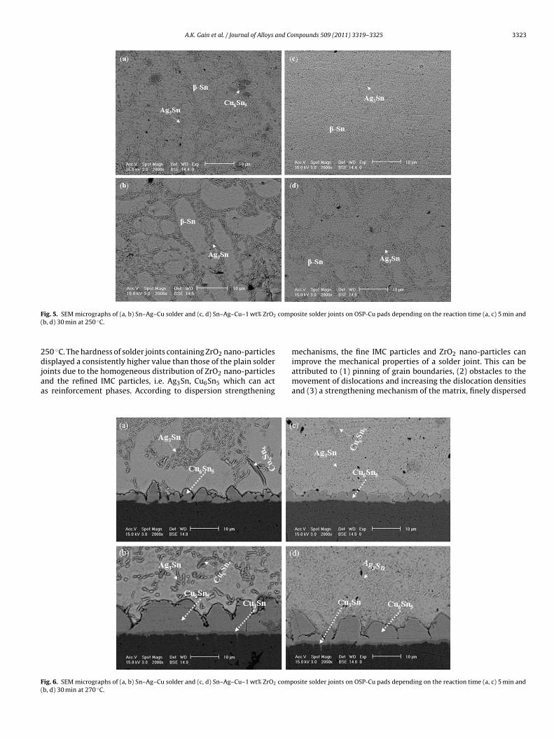
A.K. Gain et al. / Journal of Alloys and Compounds 509 (2011) 3319–3325 3323
F comp(
2djaa
F(
ig. 5. SEM micrographs of (a, b) Sn–Ag–Cu solder and (c, d) Sn–Ag–Cu–1 wt% ZrO2
b, d) 30 min at 250 ◦C.
50 ◦C. The hardness of solder joints containing ZrO2 nano-particles
isplayed a consistently higher value than those of the plain solderoints due to the homogeneous distribution of ZrO2 nano-particlesnd the refined IMC particles, i.e. Ag3Sn, Cu6Sn5 which can acts reinforcement phases. According to dispersion strengthening
ig. 6. SEM micrographs of (a, b) Sn–Ag–Cu solder and (c, d) Sn–Ag–Cu–1 wt% ZrO2 compb, d) 30 min at 270 ◦C.
osite solder joints on OSP-Cu pads depending on the reaction time (a, c) 5 min and
mechanisms, the fine IMC particles and ZrO2 nano-particles can
improve the mechanical properties of a solder joint. This can beattributed to (1) pinning of grain boundaries, (2) obstacles to themovement of dislocations and increasing the dislocation densitiesand (3) a strengthening mechanism of the matrix, finely dispersedosite solder joints on OSP-Cu pads depending on the reaction time (a, c) 5 min and

3324 A.K. Gain et al. / Journal of Alloys and Compounds 509 (2011) 3319–3325
Fig. 7. Thickness (d) of Cu intermetallic compounds as a function of reaction time between liquid (a) Sn–Ag–Cu and (b) Sn–Ag–Cu–1 wt% ZrO2 composite solder/OSP-Cu padsubstrates at various temperatures.
Fig. 8. Thickness (d2) of Cu intermetallic compounds as a function of reaction time between liquid (a) Sn–Ag–Cu and (b) Sn–Ag–Cu–1 wt% ZrO2 composite solder/OSP-Cupad substrates at various temperatures.
FZ
Iu1am1
The liquid-state interfacial reactions between plain Sn–Ag–Cu
ig. 9. Arrhenius plots for the IMC growth in Sn–Ag–Cu solder and Sn–Ag–Cu–1 wt%rO2 composite solder/OSP-Cu pad substrates interfacial reactions.
MC particles and ZrO2 nano-particles [26]. The microhardness val-es of the plain Sn–Ag–Cu solder joints and solder joints containingwt% of ZrO2 nano-particles after 5 min reaction at 250 ◦C were
bout 15.0 Hv and 17.1 Hv, respectively. On the other hand, theiricrohardness values after 30 min reaction at 250 ◦C were about3.7 Hv and 15.5 Hv, respectively.
Fig. 10. Hardness of plain Sn–Ag–Cu and Sn–Ag–Cu–1 wt% ZrO2 solder joints as afunction of the reaction time at 250 ◦C.
4. Conclusions
solder joints and solder joints containing ZrO2 nano-particleswith OSP-Cu pads were investigated as a function of reactiontime at various temperatures. After the reflow at various tem-

and Co
paIirp�nctcldr
aIeni
A
UHolr
[
[[[
[
[[[[
[[
[
[
A.K. Gain et al. / Journal of Alloys
eratures and different reaction times, an island-shaped Cu6Sn5nd Cu3Sn IMC layers were formed at their interfaces and theMC layers thicknesses were substantially increased with anncrease in the temperature and reaction time. In the solder ballegion, needle-shaped Ag3Sn and spherically-shaped Cu6Sn5 IMCarticles were found to be homogeneously distributed in the–Sn matrix. However, after the addition of ZrO2 nano-particles,eedle-shaped Ag3Sn and spherically-shaped Cu6Sn5 IMC parti-les appeared with a fine microstructure and also suppressedhe formation of IMC layers. From a kinetic analysis, the cal-ulated activation energies for the total (Cu6Sn5 + Cu3Sn) IMCayers for Sn–Ag–Cu and Sn–Ag–Cu–1 wt% ZrO2 composite sol-er joints on OSP-Cu pads were about 53.2 and 59.5 kJ/mol,espectively.
The solder joints containing 1 wt% ZrO2 nano-particles showedconsistently higher hardness than that of the plain solder joints.
t is reasonable to suggest that the hardness of the bulk solder wasnhanced by the addition ZrO2 nano-particles because the ZrO2ano-particles dispersion strengthened the solder as well as refin-
ng the microstructure.
cknowledgements
The authors acknowledge the financial support provided by City
niversity of Hong Kong for the project 9041222 CERG grant ofong Kong Research Grants Council and RGC ref. no. 111307 (Devel-pment of a nano-activator doped surface modifier for Sn–Zn basedead-free soldering). Professor Brian Ralph is thanked for proofeading the manuscript.[
[[[
mpounds 509 (2011) 3319–3325 3325
References
[1] S.E. Negm, H. Mady, A.A. Bahgat, J. Alloys Compd. 503 (2010) 65–70.[2] L. Liu, W. Zhou, B. Li, P. Wu, J. Alloys Compd. 482 (2009) 90–98.[3] A.K. Gain, Y.C. Chan, A. Sharif, W.K.C. Yung, Microelectron. Eng. 86 (2009)
2347–2353.[4] S.H. Wang, T.S. Chin, C.F. Yang, S.W. Chen, C.T. Chuang, J. Alloys Compd. 497
(2010) 428–431.[5] C.Y. Lin, U.S. Mohanty, J.H. Chou, J. Alloys Compd. 501 (2010) 204–210.[6] R.M. Shalaby, J. Alloys Compd. 505 (2010) 113–117.[7] C. Han, Q. Liu, D.G. Ivey, Mater. Sci. Eng. B 164 (2009) 172–179.[8] W. Tang, H. Zang, Y. Wu, Z. Zheng, J. Alloys Compd. 497 (2010) 396–401.[9] J. Shen, Y.C. Chan, J. Alloys Compd. 477 (2009) 909–914.10] T. Fouzder, A.K. Gain, Y.C. Chan, A. Sharif, N.B. Wong, W.K.C. Yung, Microelec-
tron. Reliab. 50 (2010) 2051–2058.11] J. Shen, Y.C. Chan, J. Alloys Compd. 477 (2009) 552–559.12] B.I. Noh, J.H. Choi, J.W. Yoon, S.B. Jung, J. Alloys Compd. 499 (2010) 154–159.13] F. Tai, F. Guo, M.T. Han, Z.D. Xia, Y.P. Lei, Y.W. Shi, Mater. Sci. Eng. A 527 (2010)
3335–3342.14] W.M. Xiao, Y.W. Shi, G.C. Xu, R. Ren, F. Guo, Z.D. Xia, Y.P. Lei, J. Alloys Compd.
472 (2009) 198–202.15] L.C. Tsao, S.Y. Chang, Mater. Des. 31 (2010) 990–993.16] C.C. Chang, Y.W. Lin, Y.W. Wang, C.R. Kao, J. Alloys Compd. 492 (2010) 99–104.17] M.H. Tsai, W.M. Chen, M.Y. Tsai, C.R. Kao, J. Alloys Compd. 504 (2010) 341–344.18] F. Cheng, F. Gao, H. Nishikawa, T. Takemoto, J. Alloys Compd. 472 (2009)
530–534.19] P. Liu, p. Yao, J. Liu, J. Alloys Compd. 486 (2009) 474–479.20] J.I. Goldstein, D.E. Newbury, P. Echlin, D.C. Joy, A.D. Romig Jr., C.E. Lyman, C.
Fiori, E. Lifshin, Scanning Electron Microscopy and X-ray Microanalysis, 2nded., Plenum, New York, 1992.
21] J.W. Yoon, B.I. Noh, B.K. Kim, C.C. Shur, S.B. Jung, J. Alloys Compd. 486 (2009)142–147.
22] L.C. Tsao, J. Alloys Compd. (2010), doi:10.1016/j.jallcom.2010.11.010.
23] B. Li, Y.W. Shi, Y.P. Lei, F. Guo, Z.D. Xia, B. Zong, J. Electron. Mater. 34 (3) (2005)217–224.24] A. Sharif, Y.C. Chan, M.N. Islam, M.J. Rizvi, J. Alloys Compd. 388 (2005) 75–82.25] M.C. Wang, S.P. Yu, T.C. Chang, M.H. Hon, J. Alloys Compd. 381 (2004) 162–167.26] Y. Shi, J. Liu, Z. Xia, Y. Lei, F. Guo, X. Li, J. Mater. Sci. Mater. Electron. 19 (2008)
349–356.


![Journal of Alloys and Compounds - · PDF file Journal of Alloys and Compounds 509 (2011) ... a College of Math and Physics, ... the below formula [17]:](https://static.fdocuments.in/doc/165x107/5aa05da77f8b9a62178e072c/journal-of-alloys-and-compounds-journal-of-alloys-and-compounds-509-2011-.jpg)


![Journal of Alloys and Compounds - nimte.ac.cn...thermal transport properties between magnetic refrigerants and heat-exchange medium [24]. Therefore, the Fe-based glassy alloys with](https://static.fdocuments.in/doc/165x107/60d2bd31873414242c6a7eb3/journal-of-alloys-and-compounds-nimteaccn-thermal-transport-properties-between.jpg)