JN5189: IEEE 802.15.4 low power wireless MCU · NXP Semiconductors IEEE 802.15.4 low power wireless...
92
1. General description The JN5189 and JN5189T (called JN5189 throughout this document) are ultra-low power, high performance Arm ® Cortex ® -M4 based wireless microcontrollers supporting ZigBee 3.0 networking stack to facilitate the development of Home Automation, Light Link and Remote control applications. The JN5189 includes a 2.4 GHz IEEE 802.15.4 compliant transceiver and a comprehensive mix of analog and digital peripherals. Ultra-low current consumption in both radio receive and transmit modes and also in the power down modes allow use of coin cell batteries. The product has 640 KB embedded Flash, 152 KB RAM memory. The embedded flash can support Over The Air (OTA) code download of applications. The devices include 10-channel PWM, two timers, one RTC/alarm timer, a Windowed Watchdog Timer (WWDT), two USARTs, two SPI interfaces, two I2C interfaces, a DMIC subsystem with dual-channel PDM microphone interface with voice activity detector, one 12-bit ADC, temperature sensor and comparator. The JN5189T variant has an internal NFC tag and with connections to the external NFC antenna. The JN5188 variant has the same functionality as the JN5189 except for reduced memory sizes of 320 KB embedded Flash, 88 KB RAM. The JN5188T variant has the functionality of the JN5188 with the addition of an embedded NFC tag. The Arm Cortex-M4 is a 32-bit core that offers system enhancements such as low power consumption, enhanced debug features, and a high level support of the block integration. The Arm Cortex-M4 CPU, operates at up to 48 MHz. 2. Features and benefits 2.1 Benefits Very low current solution for long battery life Single chip device to run stack and application System BOM is low in component count and cost Flexible sensor interfacing Embedded NTAG on JN5189T and JN5188T devices Package 6 6 mm HVQFN40, 0.5 mm pitch Lead-free and RoHS compliant Junction temperature range: 40 C to +125 C JN5189 IEEE 802.15.4 low power wireless MCU Rev. 1.1 — 22 February 2020 product data sheet JN5189
Transcript of JN5189: IEEE 802.15.4 low power wireless MCU · NXP Semiconductors IEEE 802.15.4 low power wireless...
1. General description
The JN5189 and JN5189T (called JN5189 throughout this document) are ultra-low power,high performance Arm® Cortex®-M4 based wireless microcontrollers supportingZigBee 3.0 networking stack to facilitate the development of Home Automation, Light Linkand Remote control applications.
The JN5189 includes a 2.4 GHz IEEE 802.15.4 compliant transceiver and a comprehensive mix of analog and digital peripherals. Ultra-low current consumption in both radio receive and transmit modes and also in the power down modes allow use of coin cell batteries.
The product has 640 KB embedded Flash, 152 KB RAM memory. The embedded flash can support Over The Air (OTA) code download of applications. The devices include 10-channel PWM, two timers, one RTC/alarm timer, a Windowed Watchdog Timer (WWDT), two USARTs, two SPI interfaces, two I2C interfaces, a DMIC subsystem with dual-channel PDM microphone interface with voice activity detector, one 12-bit ADC, temperature sensor and comparator.
The JN5189T variant has an internal NFC tag and with connections to the external NFC antenna.
The JN5188 variant has the same functionality as the JN5189 except for reduced memory sizes of 320 KB embedded Flash, 88 KB RAM. The JN5188T variant has the functionality of the JN5188 with the addition of an embedded NFC tag.
The Arm Cortex-M4 is a 32-bit core that offers system enhancements such as low power consumption, enhanced debug features, and a high level support of the block integration. The Arm Cortex-M4 CPU, operates at up to 48 MHz.
2. Features and benefits
2.1 Benefits Very low current solution for long battery life Single chip device to run stack and application System BOM is low in component count and cost Flexible sensor interfacing Embedded NTAG on JN5189T and JN5188T devices Package 6 6 mm HVQFN40, 0.5 mm pitch Lead-free and RoHS compliant
Junction temperature range: 40 C to +125 C
JN5189IEEE 802.15.4 low power wireless MCURev. 1.1 — 22 February 2020 product data sheet
JN518
9
NXP Semiconductors IEEE 802.15.4 low power wirelessJN5189
2.2 Radio features 2.4 GHz IEEE 802.15.4 2011 compliant Receiver current 4.3 mA IEEE 802.15.4 Receiver sensitivity 100 dBm Improved co-existence with WiFi Configurable transmit power up to +11 dBm, with 46 dB range Transmit power / current +10 dBm / 20.28 mA Transmit power / current +3 dBm / 9.44 mA Transmit power / current 0 dBm / 7.36 mA 1.9 V to 3.6 V supply voltage Antenna Diversity control 32 MHz XTAL cell with internal capacitors, able with suitable external XTAL to meet
the required accuracy for radio operation over the operating conditions Integrated RF balun Integrated ultra Low-power sleep oscillator Deep Power-down current 350 nA (with wake-up from IO) 128-bit or 256-bit AES security processor MAC accelerator with packet formatting, CRCs, address check, auto-acks, timers
2.3 Microcontroller features Application CPU, Arm Cortex-M4 CPUs: Arm Cortex-M4 processor, running at a frequency of up to 48 MHz. Arm built-in Nested Vectored Interrupt Controller (NVIC) Memory Protection Unit (MPU) Non-maskable Interrupt (NMI) with a selection of sources Serial Wire Debug (SWD) with 8 breakpoints and 4 watchpoints System tick timer Includes Serial Wire Output for enhanced debug capabilities.
On-Chip memory 640 KB flash (320 KB for JN5188) 152 KB SRAM (88 KB for JN5188)
12 MHz to 48 MHz system clock speed for low-power 2 x I2C-bus interface, operate as either master or slave 10 x PWM 2 x Low-power timers 2 x USART, one with flow control 2 x SPI-bus, master or slave 1 x PDM digital audio interface with a hardware based voice activity detector to reduce
power consumption in voice applications. Support for dual-channel microphone interface, flexible decimators, 16 entry FIFOs and optional DC blocking.
19-channel DMA engine for efficient data transfer between peripherals and SRAM, or SRAM to SRAM. DMA can operate with fixed or incrementing addresses. Operations can be chained together to provide complex functionality with low CPU overhead.
JN5189 All information provided in this document is subject to legal disclaimers. © NXP B.V. 2020. All rights reserved.
Product data sheet Rev. 1.1 — 22 February 2020 2 of 92

NXP Semiconductors IEEE 802.15.4 low power wirelessJN5189
Up to four GPIOs can be selected as pin interrupts (PINT), triggered by rising, falling or both input edges.
Two GPIO grouped interrupts (GINT) enable an interrupt based on a logical (AND/OR) combination of input states.
32-bit Real Time clock (RTC) with 1 s resolution. A timer in the RTC can be used to wake from Sleep, Deep-sleep and Power-down, with 1 ms resolution
Voltage Brown Out with 8 programmable thresholds 8-input 12-bit ADC, 190 kS/sec. HW support for continuous operation or single
conversions, single or multiple inputs can be sampled within a sequence. DMA operation can be linked to achieve low overhead operation.
1 x analog comparator Battery and temperature sensors Watchdog timer and POR Standby power controller Up to 22 Digital IOs (DIO) 1 x Quad SPIFI for accessing an external flash device either through register accesses
or for direct execution of code NTAG NFC Forum Type 2 on JN5189T and JN5188T only Random Number Generator engine AES engine AES-128 to 256 Hash hardware accelerator support SHA-1 and SHA-256 EFuse: 128-bit random AES key configuration modes Trimming
ISO7816 smart card digital interface which with a suitable external analogue device can operate as a smart card reader
2.4 Low power features Sleep mode supported, one or both CPUs in low power state waiting for interrupt Deep-sleep mode supported, both CPUs in low power state waiting for interrupt, but
extra functionality disabled or in low power state compared to sleep mode Power Down mode, main functionality powered down, wakeup possible from IOs,
wakeup possible from some peripherals (I2C, USART, SPI) in a limited function mode and low power timers
Deep -power down, very low power state with option of wake-up triggered by IOs, 350 nA
41-bit and 28-bit Low power timers can run in power down mode, clocked by 32 kHz FRO or 32 kHz XTAL. Timers can run for over one year or 2 days
3. Applications
ZigBee 3.0, networks Robust and secure Low-power wireless applications Lighting and Home automation ZigBee Light Link networks
JN5189 All information provided in this document is subject to legal disclaimers. © NXP B.V. 2020. All rights reserved.
Product data sheet Rev. 1.1 — 22 February 2020 3 of 92
NXP Semiconductors IEEE 802.15.4 low power wirelessJN5189
Toys and gaming peripherals Energy harvesting, for example self-powered light switch
4. Ordering information
5. Marking
Table 1. Ordering information Type number Package
Name Description VersionJN5189HN HVQFN40 Plastic thermal enhanced very thin quad
flat package; no leads; 40 terminals; body 6 6 0.85 mm
SOT618-1JN5189THNJN5188HNJN5188THN
Table 2. Ordering information details Type number Flash size SRAM size NTAG
JN5189HN 640 KB 152 KB noJN5189THN yesJN5188HN 320 KB 88 KB noJN5188THN yes
Table 3. Marking codes Type number Marking code
JN5189HN JN5189
JN5189THN JN5189T
JN5188HN JN5188
JN5188THN JN5188T
JN5189 All information provided in this document is subject to legal disclaimers. © NXP B.V. 2020. All rights reserved.
Product data sheet Rev. 1.1 — 22 February 2020 4 of 92
NXP Semiconductors IEEE 802.15.4 low power wirelessJN5189
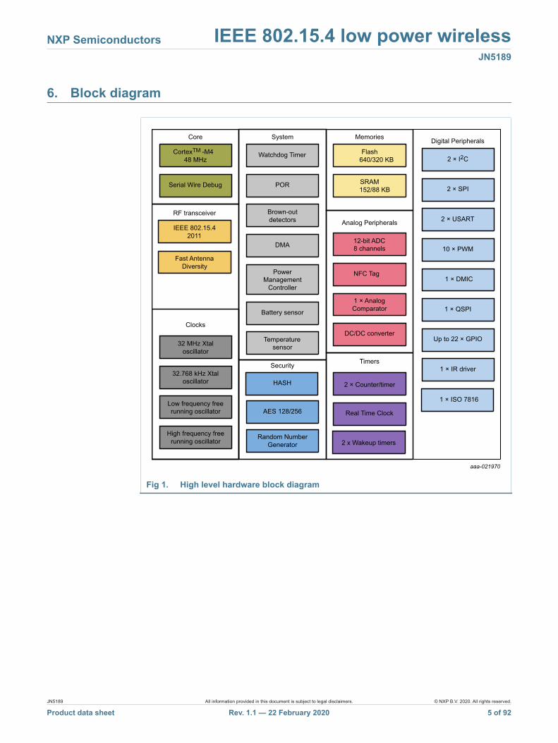
6. Block diagram
Fig 1. High level hardware block diagram
aaa-021970
CortexTM -M448 MHz
Brown-outdetectors
Temperaturesensor
Random NumberGenerator
PowerManagement
Controller
Serial Wire Debug
Core
Flash640/320 KB
SRAM152/88 KB
Memories
12-bit ADC8 channels
NFC Tag
1 × AnalogComparator
Analog Peripherals
2 × SPI
2 × USART
10 × PWM
1 × DMIC
1 × QSPI
Up to 22 × GPIO
1 × IR driver
2 × I2C
Digital Peripherals
POR
DMA
Battery sensor
DC/DC converter
Watchdog Timer
System
Low frequency freerunning oscillator
32 MHz Xtaloscillator
32.768 kHz Xtaloscillator
High frequency freerunning oscillator
Clocks
AES 128/256
Security
Real Time Clock
2 × Counter/timer
Timers
Fast AntennaDiversity
RF transceiver
IEEE 802.15.42011
HASH
1 × ISO 7816
2 x Wakeup timers
JN5189 All information provided in this document is subject to legal disclaimers. © NXP B.V. 2020. All rights reserved.
Product data sheet Rev. 1.1 — 22 February 2020 5 of 92
NXP Semiconductors IEEE 802.15.4 low power wirelessJN5189
7. Pinning information
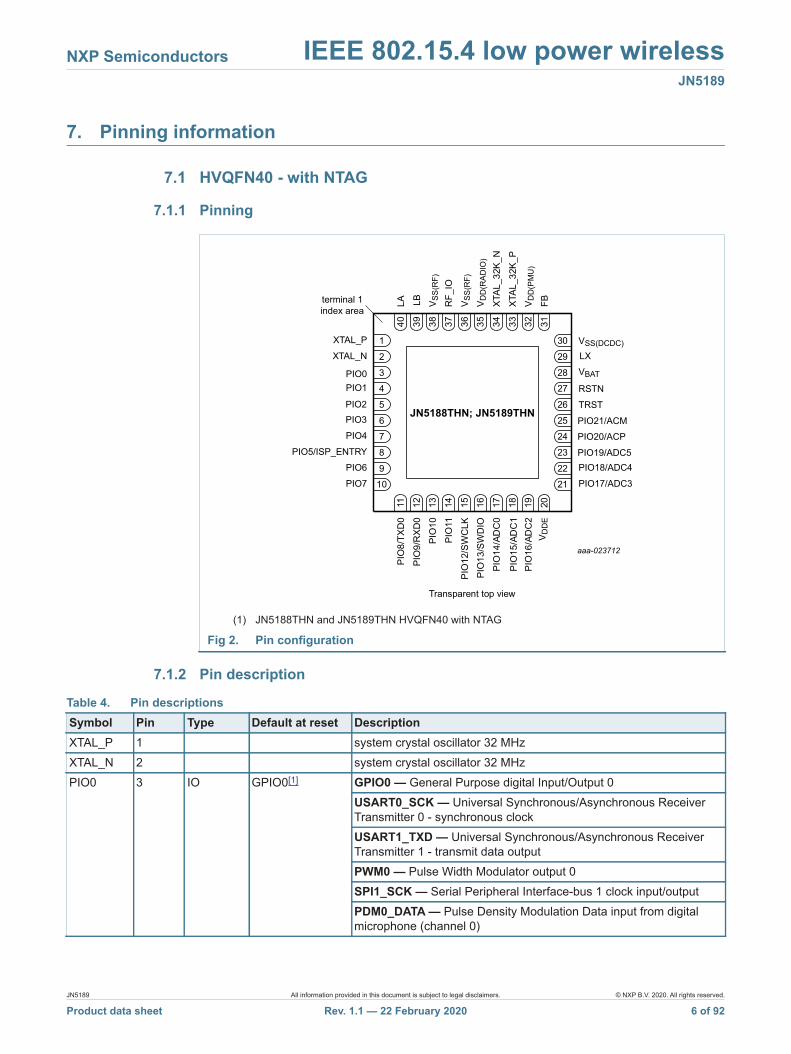
7.1 HVQFN40 - with NTAG
7.1.1 Pinning
7.1.2 Pin description
(1) JN5188THN and JN5189THN HVQFN40 with NTAG
Fig 2. Pin configuration
aaa-023712
10 219 22
8 23
7 246 25
5 26
4 273 28
2 29
1 30
11 12 13 14 15 16 17 18 19 20
40 39 38 37 36 35 34 33 32 31
terminal 1index area
Transparent top view
PIO7
PIO6PIO5/ISP_ENTRY
PIO1
XTAL_N
XTAL_P
PIO0
PIO3PIO2
PIO4
PIO
8/TX
D0
PIO
9/R
XD0
PIO
10
PIO
11
PIO
12/S
WC
LKPI
O13
/SW
DIO
PIO
15/A
DC
1
V DD
E
PIO
14/A
DC
0
PIO
16/A
DC
2
PIO17/ADC3
PIO18/ADC4
TRST
RSTN
VBAT
VSS(DCDC)LX
PIO19/ADC5
PIO20/ACPPIO21/ACM
V SS
(RF)
RF_
IO
V SS
(RF)
V DD
(RA
DIO
)
XTAL
_32K
_N
XTAL
_32K
_PV D
D(P
MU
)
FBLBLAJN5188THN; JN5189THN
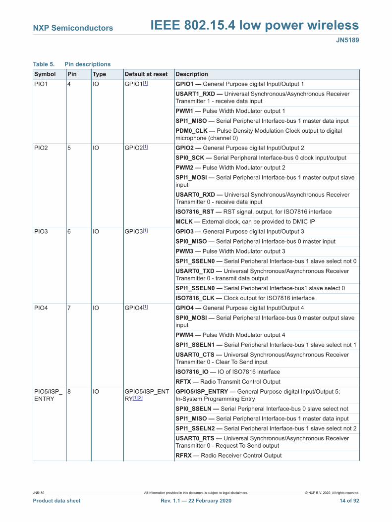
Table 4. Pin descriptionsSymbol Pin Type Default at reset DescriptionXTAL_P 1 system crystal oscillator 32 MHzXTAL_N 2 system crystal oscillator 32 MHzPIO0 3 IO GPIO0[1] GPIO0 — General Purpose digital Input/Output 0
USART0_SCK — Universal Synchronous/Asynchronous Receiver Transmitter 0 - synchronous clockUSART1_TXD — Universal Synchronous/Asynchronous Receiver Transmitter 1 - transmit data outputPWM0 — Pulse Width Modulator output 0SPI1_SCK — Serial Peripheral Interface-bus 1 clock input/outputPDM0_DATA — Pulse Density Modulation Data input from digital microphone (channel 0)
JN5189 All information provided in this document is subject to legal disclaimers. © NXP B.V. 2020. All rights reserved.
Product data sheet Rev. 1.1 — 22 February 2020 6 of 92

NXP Semiconductors IEEE 802.15.4 low power wirelessJN5189
PIO1 4 IO GPIO1[1] GPIO1 — General Purpose digital Input/Output 1USART1_RXD — Universal Synchronous/Asynchronous Receiver Transmitter 1 - receive data inputPWM1 — Pulse Width Modulator output 1SPI1_MISO — Serial Peripheral Interface-bus 1 master data inputPDM0_CLK — Pulse Density Modulation Clock output to digital microphone (channel 0)
PIO2 5 IO GPIO2[1] GPIO2 — General Purpose digital Input/Output 2SPI0_SCK — Serial Peripheral Interface-bus 0 clock input/outputPWM2 — Pulse Width Modulator output 2SPI1_MOSI — Serial Peripheral Interface-bus 1 master output slave inputUSART0_RXD — Universal Synchronous/Asynchronous Receiver Transmitter 0 - receive data inputISO7816_RST — RST signal, output, for ISO7816 interfaceMCLK — External clock, can be provided to DMIC IP
PIO3 6 IO GPIO3[1] GPIO3 — General Purpose digital Input/Output 3SPI0_MISO — Serial Peripheral Interface-bus 0 master inputPWM3 — Pulse Width Modulator output 3SPI1_SSELN0 — Serial Peripheral Interface-bus 1 slave select not 0USART0_TXD — Universal Synchronous/Asynchronous Receiver Transmitter 0 - transmit data outputSPI1_SSELN0 — Serial Peripheral Interface-bus1 slave select 0ISO7816_CLK — Clock output for ISO7816 interface
PIO4 7 IO GPIO4[1] GPIO4 — General Purpose digital Input/Output 4SPI0_MOSI — Serial Peripheral Interface-bus 0 master output slave inputPWM4 — Pulse Width Modulator output 4SPI1_SSELN1 — Serial Peripheral Interface-bus 1 slave select not 1USART0_CTS — Universal Synchronous/Asynchronous Receiver Transmitter 0 - Clear To Send inputISO7816_IO — IO of ISO7816 interfaceRFTX — Radio Transmit Control Output
PIO5/ISP_ENTRY
8 IO GPIO5/ISP_ENTRY[1][2]
GPIO5/ISP_ENTRY — General Purpose digital Input/Output 5; In-System Programming EntrySPI0_SSELN — Serial Peripheral Interface-bus 0 slave select notSPI1_MISO — Serial Peripheral Interface-bus 1 master data inputSPI1_SSELN2 — Serial Peripheral Interface-bus 1 slave select not 2USART0_RTS — Universal Synchronous/Asynchronous Receiver Transmitter 0 - Request To Send outputRFRX — Radio Receiver Control Output
Table 4. Pin descriptionsSymbol Pin Type Default at reset Description
JN5189 All information provided in this document is subject to legal disclaimers. © NXP B.V. 2020. All rights reserved.
Product data sheet Rev. 1.1 — 22 February 2020 7 of 92

NXP Semiconductors IEEE 802.15.4 low power wirelessJN5189
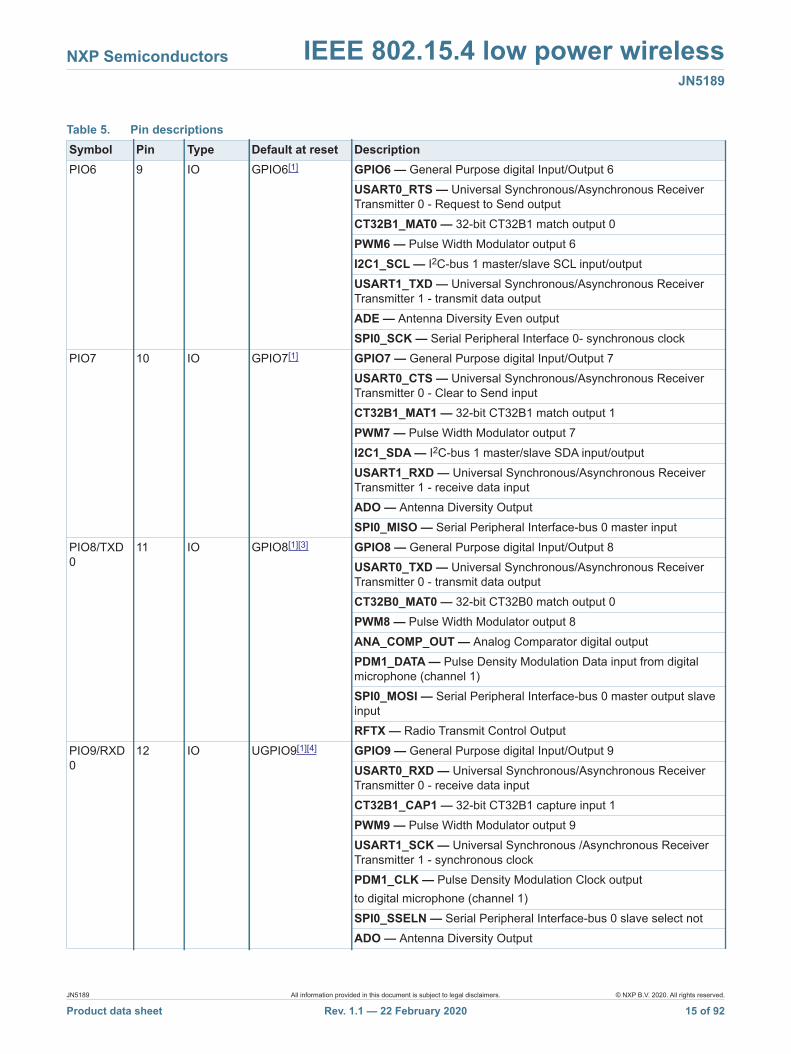
PIO6 9 IO GPIO6[1] GPIO6 — General Purpose digital Input/Output 6USART0_RTS — Universal Synchronous/Asynchronous Receiver Transmitter 0 - Request to Send outputCT32B1_MAT0 — 32-bit CT32B1 match output 0PWM6 — Pulse Width Modulator output 6I2C1_SCL — I2C-bus 1 master/slave SCL input/outputUSART1_TXD — Universal Synchronous/Asynchronous Receiver Transmitter 1 - transmit data outputADE — Antenna Diversity Even outputSPI0_SCK — Serial Peripheral Interface 0- synchronous clock
PIO7 10 IO GPIO7[1] GPIO7 — General Purpose digital Input/Output 7USART0_CTS — Universal Synchronous/Asynchronous Receiver Transmitter 0 - Clear to Send inputCT32B1_MAT1 — 32-bit CT32B1 match output 1PWM7 — Pulse Width Modulator output 7I2C1_SDA — I2C-bus 1 master/slave SDA input/outputUSART1_RXD — Universal Synchronous/Asynchronous Receiver Transmitter 1 - receive data inputADO — Antenna Diversity OutputSPI0_MISO — Serial Peripheral Interface-bus 0 master input
PIO8/TXD0
11 IO GPIO8[1][3] GPIO8 — General Purpose digital Input/Output 8USART0_TXD — Universal Synchronous/Asynchronous Receiver Transmitter 0 - transmit data outputCT32B0_MAT0 — 32-bit CT32B0 match output 0PWM8 — Pulse Width Modulator output 8ANA_COMP_OUT — Analog Comparator digital outputPDM1_DATA — Pulse Density Modulation Data input from digital microphone (channel 1)SPI0_MOSI — Serial Peripheral Interface-bus 0 master output slave inputRFTX — Radio Transmit Control Output
PIO9/RXD0
12 IO GPIO9[1][4] GPIO9 — General Purpose digital Input/Output 9USART0_RXD — Universal Synchronous/Asynchronous Receiver Transmitter 0 - receive data inputCT32B1_CAP1 — 32-bit CT32B1 capture input 1PWM9 — Pulse Width Modulator output 9USART1_SCK — Universal Synchronous /Asynchronous Receiver Transmitter 1 - synchronous clockPDM1_CLK — Pulse Density Modulation Clock outputto digital microphone (channel 1)SPI0_SSELN — Serial Peripheral Interface-bus 0 slave select notADO — Antenna Diversity Output
Table 4. Pin descriptionsSymbol Pin Type Default at reset Description
JN5189 All information provided in this document is subject to legal disclaimers. © NXP B.V. 2020. All rights reserved.
Product data sheet Rev. 1.1 — 22 February 2020 8 of 92

NXP Semiconductors IEEE 802.15.4 low power wirelessJN5189
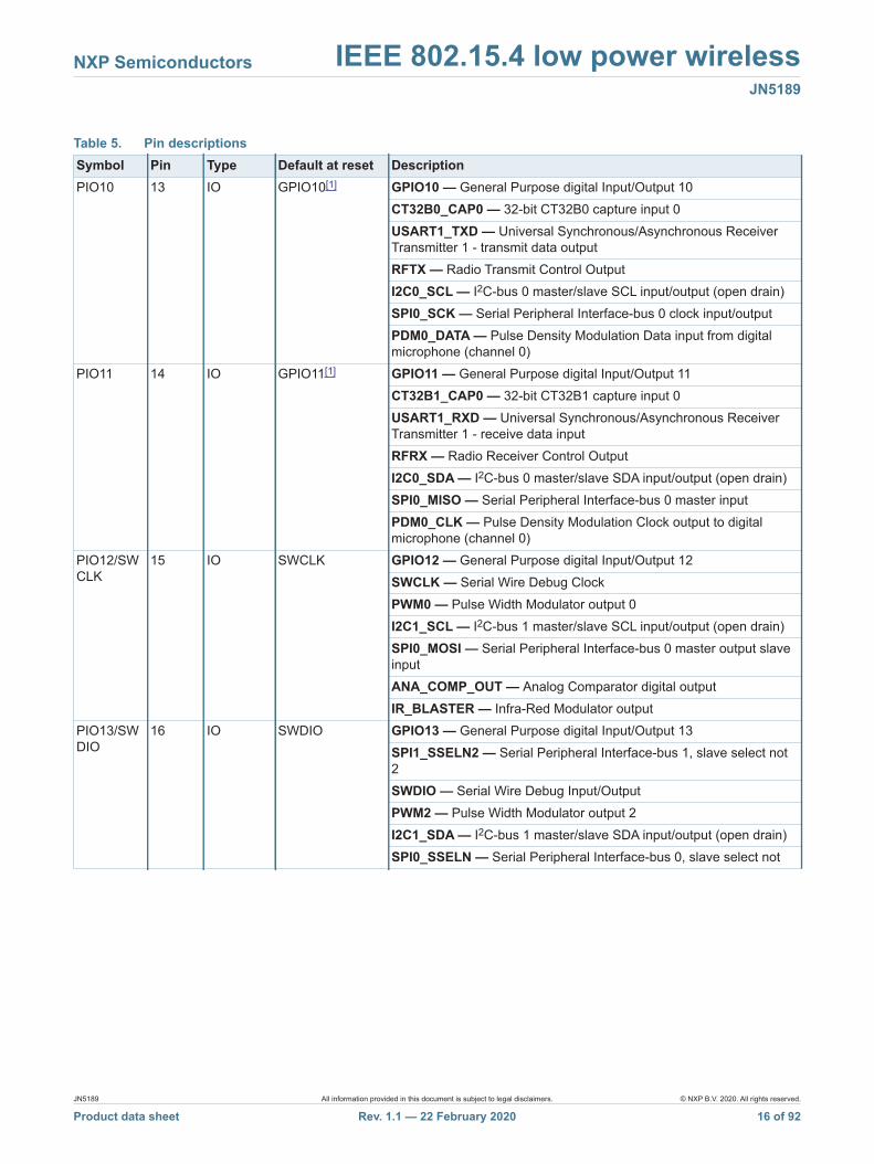
PIO10 13 IO GPIO10[1] GPIO10 — General Purpose digital Input/Output 10CT32B0_CAP0 — 32-bit CT32B0 capture input 0USART1_TXD — Universal Synchronous/Asynchronous Receiver Transmitter 1 - transmit data outputRFTX — Radio Transmit Control OutputI2C0_SCL — I2C-bus 0 master/slave SCL input/output (open drain)SPI0_SCK — Serial Peripheral Interface-bus 0 clock input/outputPDM0_DATA — Pulse Density Modulation Data input from digital microphone (channel 0)
PIO11 14 IO GPIO11[1] GPIO11 — General Purpose digital Input/Output 11CT32B1_CAP0 — 32-bit CT32B1 capture input 0USART1_RXD — Universal Synchronous/Asynchronous Receiver Transmitter 1 - receive data inputRFRX — Radio Receiver Control OutputI2C0_SDA — I2C-bus 0 master/slave SDA input/output (open drain)SPI0_MISO — Serial Peripheral Interface-bus 0 master inputPDM0_CLK — Pulse Density Modulation Clock output to digital microphone (channel 0)
PIO12/SWCLK
15 IO SWCLK GPIO12 — General Purpose digital Input/Output 12SWCLK — Serial Wire Debug ClockPWM0 — Pulse Width Modulator output 0I2C1_SCL — I2C-bus 1 master/slave SCL input/output (open drain)SPI0_MOSI — Serial Peripheral Interface-bus 0 master output slave inputANA_COMP_OUT — Analog Comparator digital outputIR_BLASTER — Infra-Red Modulator output
PIO13/SWDIO
16 IO SWDIO GPIO13 — General Purpose digital Input/Output 13SPI1_SSELN2 — Serial Peripheral Interface-bus 1, slave select not 2SWDIO — Serial Wire Debug Input/OutputPWM2 — Pulse Width Modulator output 2I2C1_SDA — I2C-bus 1 master/slave SDA input/output (open drain)SPI0_SSELN — Serial Peripheral Interface-bus 0, slave select not
Table 4. Pin descriptionsSymbol Pin Type Default at reset Description
JN5189 All information provided in this document is subject to legal disclaimers. © NXP B.V. 2020. All rights reserved.
Product data sheet Rev. 1.1 — 22 February 2020 9 of 92

NXP Semiconductors IEEE 802.15.4 low power wirelessJN5189
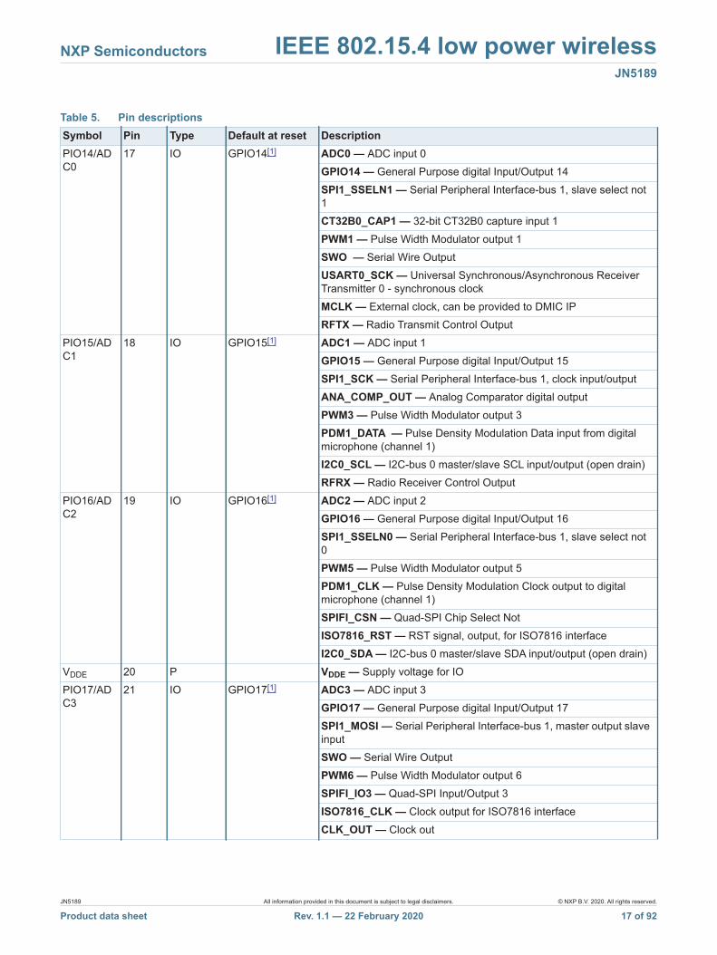
PIO14/ADC0
17 IO GPIO14[1] ADC0 — ADC input 0GPIO14 — General Purpose digital Input/Output 14SPI1_SSELN1 — Serial Peripheral Interface-bus 1, slave select not 1CT32B0_CAP1 — 32-bit CT32B0 capture input 1PWM1 — Pulse Width Modulator output 1SWO — Serial Wire OutputUSART0_SCK — Universal Synchronous/Asynchronous Receiver Transmitter 0 - synchronous clockMCLK — External clock, can be provided to DMIC IP RFTX — Radio Transmit Control Output
PIO15/ADC1
18 IO GPIO15[1] ADC1 — ADC input 1GPIO15 — General Purpose digital Input/Output 15SPI1_SCK — Serial Peripheral Interface-bus 1, clock input/outputANA_COMP_OUT — Analog Comparator digital outputPWM3 — Pulse Width Modulator output 3PDM1_DATA — Pulse Density Modulation Data input from digital microphone (channel 1)I2C0_SCL — I2C-bus 0 master/slave SCL input/output (open drain)RFRX — Radio Receiver Control Output
PIO16/ADC2
19 IO GPIO16[1] ADC2 — ADC input 2GPIO16 — General Purpose digital Input/Output 16SPI1_SSELN0 — Serial Peripheral Interface-bus 1, slave select not 0PWM5 — Pulse Width Modulator output 5PDM1_CLK — Pulse Density Modulation Clock output to digital microphone (channel 1)SPIFI_CSN — Quad-SPI Chip Select NotISO7816_RST — RST signal, output, for ISO7816 interfaceI2C0_SDA — I2C-bus 0 master/slave SDA input/output (open drain)
VDDE 20 P VDDE — Supply voltage for IOPIO17/ADC3
21 IO GPIO17[1] ADC3 — ADC input 3GPIO17 — General Purpose digital Input/Output 17SPI1_MOSI — Serial Peripheral Interface-bus 1, master output slave inputSWO — Serial Wire OutputPWM6 — Pulse Width Modulator output 6SPIFI_IO3 — Quad-SPI Input/Output 3ISO7816_CLK — Clock output for ISO7816 interfaceCLK_OUT — Clock out
Table 4. Pin descriptionsSymbol Pin Type Default at reset Description
JN5189 All information provided in this document is subject to legal disclaimers. © NXP B.V. 2020. All rights reserved.
Product data sheet Rev. 1.1 — 22 February 2020 10 of 92
NXP Semiconductors IEEE 802.15.4 low power wirelessJN5189
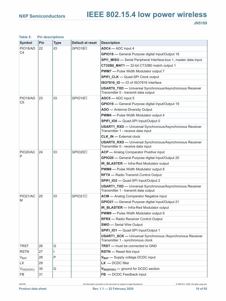
PIO18/ADC4
22 IO GPIO18[1] ADC4 — ADC input 4GPIO18 — General Purpose digital Input/Output 18SPI1_MISO — Serial Peripheral Interface-bus 1, master data inputCT32B0_MAT1 — 32-bit CT32B0 match output 1PWM7 — Pulse Width Modulator output 7SPIFI_CLK — Quad-SPI Clock outputISO7816_IO — IO of ISO7816 interfaceUSART0_TXD — Universal Synchronous/Asynchronous Receiver Transmitter 0 - transmit data output
PIO19/ADC5
23 IO GPIO19[1] ADC5 — ADC input 5GPIO19 — General Purpose digital Input/Output 19ADO — Antenna Diversity OutputPWM4 — Pulse Width Modulator output 4SPIFI_IO0 — Quad-SPI Input/Output 0USART1_RXD — Universal Synchronous/Asynchronous Receiver Transmitter 1 - receive data inputCLK_IN — External clockUSART0_RXD — Universal Synchronous/Asynchronous Receiver Transmitter 0 - receive data input
PIO20/ACP
24 IO GPIO20[1] ACP — Analog Comparator Positive inputGPIO20 — General Purpose digital Input/Output 20IR_BLASTER — Infra-Red Modulator outputPWM8 — Pulse Width Modulator output 8RFTX — Radio Transmit Control OutputSPIFI_IO2 — Quad-SPI Input/Output 2USART1_TXD — Universal Synchronous/Asynchronous Receiver Transmitter 1 - transmit data output
PIO21/ACM
25 IO GPIO21[1] ACM — Analog Comparator Negative inputGPIO21 — General Purpose digital Input/Output 21IR_BLASTER — Infra-Red Modulator outputPWM9 — Pulse Width Modulator output 9RFRX — Radio Receiver Control OutputSWO — Serial Wire OutputSPIFI_IO1 — Quad-SPI Input/Output 1USART1_SCK — Universal Synchronous /Asynchronous Receiver Transmitter 1 - synchronous clock
TRST 26 G TRST — must be connected to GNDRSTN 27 I RSTN — Reset Not inputVBAT 28 P VBAT — Supply voltage DCDC inputLX 29 LX — DCDC filterVSS(DCDC) 30 G VSS(DCDC) — ground for DCDC sectionFB 31 FB — DCDC Feedback input
Table 4. Pin descriptionsSymbol Pin Type Default at reset Description
JN5189 All information provided in this document is subject to legal disclaimers. © NXP B.V. 2020. All rights reserved.
Product data sheet Rev. 1.1 — 22 February 2020 11 of 92
NXP Semiconductors IEEE 802.15.4 low power wirelessJN5189
[1] I: input at reset.
[2] ISP programming mode: leave pin floating high during reset to avoid entering UART programming mode or hold it low to program.
[3] In ISP mode, it is configured to USART0_TXD.
[4] In ISP mode, it is configured to USART0_RXD.
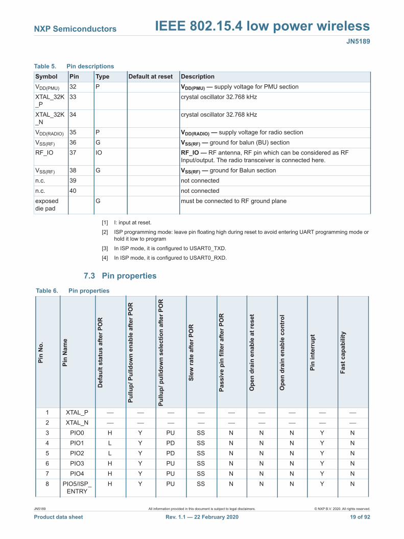
VDD(PMU) 32 P VDD(PMU) — supply voltage for PMU sectionXTAL_32K_P
33 crystal oscillator 32.768 kHz
XTAL_32K_N
34 crystal oscillator 32.768 kHz
VDD(RADIO) 35 P VDD(RADIO) — supply voltage for radio sectionVSS(RF) 36 G VSS(RF) — ground for balun (BU) sectionRF_IO 37 IO RF_IO — RF antenna, RF pin which can be considered as RF
Input/output. The radio transceiver is connected here.VSS(RF) 38 G VSS(RF} — ground for Balun sectionLB 39 NFC tag antenna input BLA 40 NFC tag antenna input Aexposed die pad
G must be connected to RF ground plane
Table 4. Pin descriptionsSymbol Pin Type Default at reset Description
JN5189 All information provided in this document is subject to legal disclaimers. © NXP B.V. 2020. All rights reserved.
Product data sheet Rev. 1.1 — 22 February 2020 12 of 92
NXP Semiconductors IEEE 802.15.4 low power wirelessJN5189
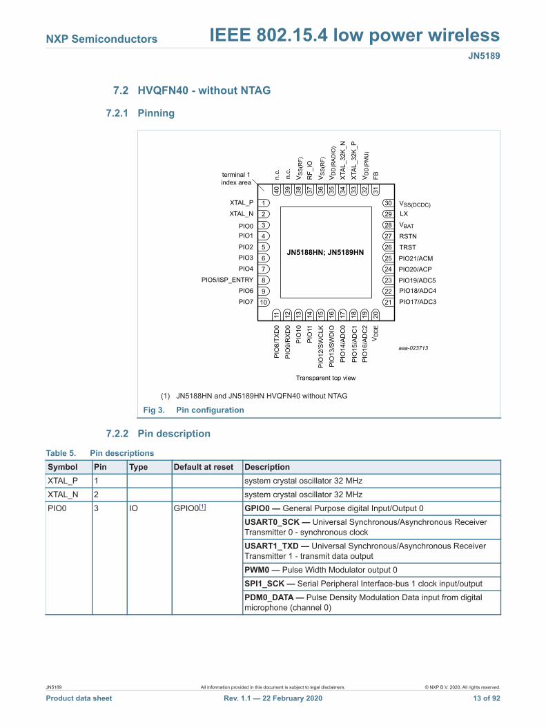
7.2 HVQFN40 - without NTAG
7.2.1 Pinning
7.2.2 Pin description
(1) JN5188HN and JN5189HN HVQFN40 without NTAG
Fig 3. Pin configuration
aaa-023713
JN5188HN; JN5189HN
10 219 22
8 23
7 246 25
5 26
4 273 28
2 29
1 30
11 12 13 14 15 16 17 18 19 20
40 39 38 37 36 35 34 33 32 31
terminal 1index area
Transparent top view
PIO7
PIO6PIO5/ISP_ENTRY
PIO1
XTAL_N
XTAL_P
PIO0
PIO3PIO2
PIO4PI
O8/
TXD
0
PIO
9/R
XD0
PIO
10
PIO
11
PIO
12/S
WC
LKPI
O13
/SW
DIO
PIO
15/A
DC
1
V DD
E
PIO
14/A
DC
0
PIO
16/A
DC
2
PIO17/ADC3
PIO18/ADC4
TRST
RSTN
VBAT
VSS(DCDC)LX
PIO19/ADC5
PIO20/ACPPIO21/ACM
V SS
(RF)
RF_
IO
V SS
(RF)
V DD
(RA
DIO
)
XTAL
_32K
_N
XTAL
_32K
_PV D
D(P
MU
)
FBn.c.
n.c.
Table 5. Pin descriptionsSymbol Pin Type Default at reset DescriptionXTAL_P 1 system crystal oscillator 32 MHzXTAL_N 2 system crystal oscillator 32 MHzPIO0 3 IO GPIO0[1] GPIO0 — General Purpose digital Input/Output 0
USART0_SCK — Universal Synchronous/Asynchronous Receiver Transmitter 0 - synchronous clockUSART1_TXD — Universal Synchronous/Asynchronous Receiver Transmitter 1 - transmit data outputPWM0 — Pulse Width Modulator output 0SPI1_SCK — Serial Peripheral Interface-bus 1 clock input/outputPDM0_DATA — Pulse Density Modulation Data input from digital microphone (channel 0)
JN5189 All information provided in this document is subject to legal disclaimers. © NXP B.V. 2020. All rights reserved.
Product data sheet Rev. 1.1 — 22 February 2020 13 of 92
NXP Semiconductors IEEE 802.15.4 low power wirelessJN5189
PIO1 4 IO GPIO1[1] GPIO1 — General Purpose digital Input/Output 1USART1_RXD — Universal Synchronous/Asynchronous Receiver Transmitter 1 - receive data inputPWM1 — Pulse Width Modulator output 1SPI1_MISO — Serial Peripheral Interface-bus 1 master data inputPDM0_CLK — Pulse Density Modulation Clock output to digital microphone (channel 0)
PIO2 5 IO GPIO2[1] GPIO2 — General Purpose digital Input/Output 2SPI0_SCK — Serial Peripheral Interface-bus 0 clock input/outputPWM2 — Pulse Width Modulator output 2SPI1_MOSI — Serial Peripheral Interface-bus 1 master output slave inputUSART0_RXD — Universal Synchronous/Asynchronous Receiver Transmitter 0 - receive data inputISO7816_RST — RST signal, output, for ISO7816 interfaceMCLK — External clock, can be provided to DMIC IP
PIO3 6 IO GPIO3[1] GPIO3 — General Purpose digital Input/Output 3SPI0_MISO — Serial Peripheral Interface-bus 0 master inputPWM3 — Pulse Width Modulator output 3SPI1_SSELN0 — Serial Peripheral Interface-bus 1 slave select not 0USART0_TXD — Universal Synchronous/Asynchronous Receiver Transmitter 0 - transmit data outputSPI1_SSELN0 — Serial Peripheral Interface-bus1 slave select 0ISO7816_CLK — Clock output for ISO7816 interface
PIO4 7 IO GPIO4[1] GPIO4 — General Purpose digital Input/Output 4SPI0_MOSI — Serial Peripheral Interface-bus 0 master output slave inputPWM4 — Pulse Width Modulator output 4SPI1_SSELN1 — Serial Peripheral Interface-bus 1 slave select not 1USART0_CTS — Universal Synchronous/Asynchronous Receiver Transmitter 0 - Clear To Send inputISO7816_IO — IO of ISO7816 interfaceRFTX — Radio Transmit Control Output
PIO5/ISP_ENTRY
8 IO GPIO5/ISP_ENTRY[1][2]
GPIO5/ISP_ENTRY — General Purpose digital Input/Output 5; In-System Programming EntrySPI0_SSELN — Serial Peripheral Interface-bus 0 slave select notSPI1_MISO — Serial Peripheral Interface-bus 1 master data inputSPI1_SSELN2 — Serial Peripheral Interface-bus 1 slave select not 2USART0_RTS — Universal Synchronous/Asynchronous Receiver Transmitter 0 - Request To Send outputRFRX — Radio Receiver Control Output
Table 5. Pin descriptionsSymbol Pin Type Default at reset Description
JN5189 All information provided in this document is subject to legal disclaimers. © NXP B.V. 2020. All rights reserved.
Product data sheet Rev. 1.1 — 22 February 2020 14 of 92
NXP Semiconductors IEEE 802.15.4 low power wirelessJN5189
PIO6 9 IO GPIO6[1] GPIO6 — General Purpose digital Input/Output 6USART0_RTS — Universal Synchronous/Asynchronous Receiver Transmitter 0 - Request to Send outputCT32B1_MAT0 — 32-bit CT32B1 match output 0PWM6 — Pulse Width Modulator output 6I2C1_SCL — I2C-bus 1 master/slave SCL input/outputUSART1_TXD — Universal Synchronous/Asynchronous Receiver Transmitter 1 - transmit data outputADE — Antenna Diversity Even outputSPI0_SCK — Serial Peripheral Interface 0- synchronous clock
PIO7 10 IO GPIO7[1] GPIO7 — General Purpose digital Input/Output 7USART0_CTS — Universal Synchronous/Asynchronous Receiver Transmitter 0 - Clear to Send inputCT32B1_MAT1 — 32-bit CT32B1 match output 1PWM7 — Pulse Width Modulator output 7I2C1_SDA — I2C-bus 1 master/slave SDA input/outputUSART1_RXD — Universal Synchronous/Asynchronous Receiver Transmitter 1 - receive data inputADO — Antenna Diversity OutputSPI0_MISO — Serial Peripheral Interface-bus 0 master input
PIO8/TXD0
11 IO GPIO8[1][3] GPIO8 — General Purpose digital Input/Output 8USART0_TXD — Universal Synchronous/Asynchronous Receiver Transmitter 0 - transmit data outputCT32B0_MAT0 — 32-bit CT32B0 match output 0PWM8 — Pulse Width Modulator output 8ANA_COMP_OUT — Analog Comparator digital outputPDM1_DATA — Pulse Density Modulation Data input from digital microphone (channel 1)SPI0_MOSI — Serial Peripheral Interface-bus 0 master output slave inputRFTX — Radio Transmit Control Output
PIO9/RXD0
12 IO UGPIO9[1][4] GPIO9 — General Purpose digital Input/Output 9USART0_RXD — Universal Synchronous/Asynchronous Receiver Transmitter 0 - receive data inputCT32B1_CAP1 — 32-bit CT32B1 capture input 1PWM9 — Pulse Width Modulator output 9USART1_SCK — Universal Synchronous /Asynchronous Receiver Transmitter 1 - synchronous clockPDM1_CLK — Pulse Density Modulation Clock outputto digital microphone (channel 1)SPI0_SSELN — Serial Peripheral Interface-bus 0 slave select notADO — Antenna Diversity Output
Table 5. Pin descriptionsSymbol Pin Type Default at reset Description
JN5189 All information provided in this document is subject to legal disclaimers. © NXP B.V. 2020. All rights reserved.
Product data sheet Rev. 1.1 — 22 February 2020 15 of 92
NXP Semiconductors IEEE 802.15.4 low power wirelessJN5189
PIO10 13 IO GPIO10[1] GPIO10 — General Purpose digital Input/Output 10CT32B0_CAP0 — 32-bit CT32B0 capture input 0USART1_TXD — Universal Synchronous/Asynchronous Receiver Transmitter 1 - transmit data outputRFTX — Radio Transmit Control OutputI2C0_SCL — I2C-bus 0 master/slave SCL input/output (open drain)SPI0_SCK — Serial Peripheral Interface-bus 0 clock input/outputPDM0_DATA — Pulse Density Modulation Data input from digital microphone (channel 0)
PIO11 14 IO GPIO11[1] GPIO11 — General Purpose digital Input/Output 11CT32B1_CAP0 — 32-bit CT32B1 capture input 0USART1_RXD — Universal Synchronous/Asynchronous Receiver Transmitter 1 - receive data inputRFRX — Radio Receiver Control OutputI2C0_SDA — I2C-bus 0 master/slave SDA input/output (open drain)SPI0_MISO — Serial Peripheral Interface-bus 0 master inputPDM0_CLK — Pulse Density Modulation Clock output to digital microphone (channel 0)
PIO12/SWCLK
15 IO SWCLK GPIO12 — General Purpose digital Input/Output 12SWCLK — Serial Wire Debug ClockPWM0 — Pulse Width Modulator output 0I2C1_SCL — I2C-bus 1 master/slave SCL input/output (open drain)SPI0_MOSI — Serial Peripheral Interface-bus 0 master output slave inputANA_COMP_OUT — Analog Comparator digital outputIR_BLASTER — Infra-Red Modulator output
PIO13/SWDIO
16 IO SWDIO GPIO13 — General Purpose digital Input/Output 13SPI1_SSELN2 — Serial Peripheral Interface-bus 1, slave select not 2SWDIO — Serial Wire Debug Input/OutputPWM2 — Pulse Width Modulator output 2I2C1_SDA — I2C-bus 1 master/slave SDA input/output (open drain)SPI0_SSELN — Serial Peripheral Interface-bus 0, slave select not
Table 5. Pin descriptionsSymbol Pin Type Default at reset Description
JN5189 All information provided in this document is subject to legal disclaimers. © NXP B.V. 2020. All rights reserved.
Product data sheet Rev. 1.1 — 22 February 2020 16 of 92
NXP Semiconductors IEEE 802.15.4 low power wirelessJN5189
PIO14/ADC0
17 IO GPIO14[1] ADC0 — ADC input 0GPIO14 — General Purpose digital Input/Output 14SPI1_SSELN1 — Serial Peripheral Interface-bus 1, slave select not 1CT32B0_CAP1 — 32-bit CT32B0 capture input 1PWM1 — Pulse Width Modulator output 1SWO — Serial Wire OutputUSART0_SCK — Universal Synchronous/Asynchronous Receiver Transmitter 0 - synchronous clockMCLK — External clock, can be provided to DMIC IP RFTX — Radio Transmit Control Output
PIO15/ADC1
18 IO GPIO15[1] ADC1 — ADC input 1GPIO15 — General Purpose digital Input/Output 15SPI1_SCK — Serial Peripheral Interface-bus 1, clock input/outputANA_COMP_OUT — Analog Comparator digital outputPWM3 — Pulse Width Modulator output 3PDM1_DATA — Pulse Density Modulation Data input from digital microphone (channel 1)I2C0_SCL — I2C-bus 0 master/slave SCL input/output (open drain)RFRX — Radio Receiver Control Output
PIO16/ADC2
19 IO GPIO16[1] ADC2 — ADC input 2GPIO16 — General Purpose digital Input/Output 16SPI1_SSELN0 — Serial Peripheral Interface-bus 1, slave select not 0PWM5 — Pulse Width Modulator output 5PDM1_CLK — Pulse Density Modulation Clock output to digital microphone (channel 1)SPIFI_CSN — Quad-SPI Chip Select NotISO7816_RST — RST signal, output, for ISO7816 interfaceI2C0_SDA — I2C-bus 0 master/slave SDA input/output (open drain)
VDDE 20 P VDDE — Supply voltage for IOPIO17/ADC3
21 IO GPIO17[1] ADC3 — ADC input 3GPIO17 — General Purpose digital Input/Output 17SPI1_MOSI — Serial Peripheral Interface-bus 1, master output slave inputSWO — Serial Wire OutputPWM6 — Pulse Width Modulator output 6SPIFI_IO3 — Quad-SPI Input/Output 3ISO7816_CLK — Clock output for ISO7816 interfaceCLK_OUT — Clock out
Table 5. Pin descriptionsSymbol Pin Type Default at reset Description
JN5189 All information provided in this document is subject to legal disclaimers. © NXP B.V. 2020. All rights reserved.
Product data sheet Rev. 1.1 — 22 February 2020 17 of 92
NXP Semiconductors IEEE 802.15.4 low power wirelessJN5189
PIO18/ADC4
22 IO GPIO18[1] ADC4 — ADC input 4GPIO18 — General Purpose digital Input/Output 18SPI1_MISO — Serial Peripheral Interface-bus 1, master data inputCT32B0_MAT1 — 32-bit CT32B0 match output 1PWM7 — Pulse Width Modulator output 7SPIFI_CLK — Quad-SPI Clock outputISO7816_IO — IO of ISO7816 interfaceUSART0_TXD — Universal Synchronous/Asynchronous Receiver Transmitter 0 - transmit data output
PIO19/ADC5
23 IO GPIO19[1] ADC5 — ADC input 5GPIO19 — General Purpose digital Input/Output 19ADO — Antenna Diversity OutputPWM4 — Pulse Width Modulator output 4SPIFI_IO0 — Quad-SPI Input/Output 0USART1_RXD — Universal Synchronous/Asynchronous Receiver Transmitter 1 - receive data inputCLK_IN — External clockUSART0_RXD — Universal Synchronous/Asynchronous Receiver Transmitter 0 - receive data input
PIO20/ACP
24 IO GPIO20[1] ACP — Analog Comparator Positive inputGPIO20 — General Purpose digital Input/Output 20IR_BLASTER — Infra-Red Modulator outputPWM8 — Pulse Width Modulator output 8RFTX — Radio Transmit Control OutputSPIFI_IO2 — Quad-SPI Input/Output 2USART1_TXD — Universal Synchronous/Asynchronous Receiver Transmitter 1 - transmit data output
PIO21/ACM
25 IO GPIO21[1] ACM — Analog Comparator Negative inputGPIO21 — General Purpose digital Input/Output 21IR_BLASTER — Infra-Red Modulator outputPWM9 — Pulse Width Modulator output 9RFRX — Radio Receiver Control OutputSWO — Serial Wire OutputSPIFI_IO1 — Quad-SPI Input/Output 1USART1_SCK — Universal Synchronous /Asynchronous Receiver Transmitter 1 - synchronous clock
TRST 26 G TRST — must be connected to GNDRSTN 27 I RSTN — Reset Not inputVBAT 28 P VBAT — Supply voltage DCDC inputLX 29 LX — DCDC filterVSS(DCDC) 30 G VSS(DCDC) — ground for DCDC sectionFB 31 FB — DCDC Feedback input
Table 5. Pin descriptionsSymbol Pin Type Default at reset Description
JN5189 All information provided in this document is subject to legal disclaimers. © NXP B.V. 2020. All rights reserved.
Product data sheet Rev. 1.1 — 22 February 2020 18 of 92
NXP Semiconductors IEEE 802.15.4 low power wirelessJN5189
[1] I: input at reset.
[2] ISP programming mode: leave pin floating high during reset to avoid entering UART programming mode or hold it low to program
[3] In ISP mode, it is configured to USART0_TXD.
[4] In ISP mode, it is configured to USART0_RXD.
7.3 Pin properties
VDD(PMU) 32 P VDD(PMU) — supply voltage for PMU sectionXTAL_32K_P
33 crystal oscillator 32.768 kHz
XTAL_32K_N
34 crystal oscillator 32.768 kHz
VDD(RADIO) 35 P VDD(RADIO) — supply voltage for radio sectionVSS(RF) 36 G VSS(RF) — ground for balun (BU) sectionRF_IO 37 IO RF_IO — RF antenna, RF pin which can be considered as RF
Input/output. The radio transceiver is connected here.VSS(RF) 38 G VSS(RF) — ground for Balun sectionn.c. 39 not connectedn.c. 40 not connectedexposed die pad
G must be connected to RF ground plane
Table 5. Pin descriptionsSymbol Pin Type Default at reset Description
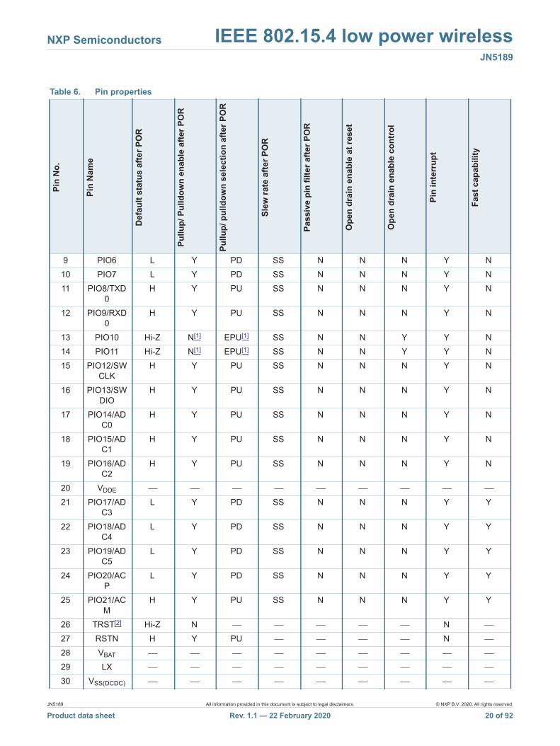
Table 6. Pin properties
Pin
No.
Pin
Nam
e
Def
ault
stat
us a
fter P
OR
Pullu
p/ P
ulld
own
enab
le a
fter P
OR
Pullu
p/ p
ulld
own
sele
ctio
n af
ter P
OR
Slew
rate
afte
r PO
R
Pass
ive
pin
filte
r afte
r PO
R
Ope
n dr
ain
enab
le a
t res
et
Ope
n dr
ain
enab
le c
ontr
ol
Pin
inte
rrup
t
Fast
cap
abili
ty
1 XTAL_P
2 XTAL_N
3 PIO0 H Y PU SS N N N Y N4 PIO1 L Y PD SS N N N Y N5 PIO2 L Y PD SS N N N Y N6 PIO3 H Y PU SS N N N Y N7 PIO4 H Y PU SS N N N Y N8 PIO5/ISP_
ENTRYH Y PU SS N N N Y N
JN5189 All information provided in this document is subject to legal disclaimers. © NXP B.V. 2020. All rights reserved.
Product data sheet Rev. 1.1 — 22 February 2020 19 of 92
NXP Semiconductors IEEE 802.15.4 low power wirelessJN5189
9 PIO6 L Y PD SS N N N Y N10 PIO7 L Y PD SS N N N Y N11 PIO8/TXD
0H Y PU SS N N N Y N
12 PIO9/RXD0
H Y PU SS N N N Y N
13 PIO10 Hi-Z N[1] EPU[1] SS N N Y Y N14 PIO11 Hi-Z N[1] EPU[1] SS N N Y Y N15 PIO12/SW
CLKH Y PU SS N N N Y N
16 PIO13/SWDIO
H Y PU SS N N N Y N
17 PIO14/ADC0
H Y PU SS N N N Y N
18 PIO15/ADC1
H Y PU SS N N N Y N
19 PIO16/ADC2
H Y PU SS N N N Y N
20 VDDE
21 PIO17/ADC3
L Y PD SS N N N Y Y
22 PIO18/ADC4
L Y PD SS N N N Y Y
23 PIO19/ADC5
L Y PD SS N N N Y Y
24 PIO20/ACP
L Y PD SS N N N Y Y
25 PIO21/ACM
H Y PU SS N N N Y Y
26 TRST[2] Hi-Z N N
27 RSTN H Y PU N
28 VBAT
29 LX
30 VSS(DCDC)
Table 6. Pin properties
Pin
No.
Pin
Nam
e
Def
ault
stat
us a
fter P
OR
Pullu
p/ P
ulld
own
enab
le a
fter P
OR
Pullu
p/ p
ulld
own
sele
ctio
n af
ter P
OR
Slew
rate
afte
r PO
R
Pass
ive
pin
filte
r afte
r PO
R
Ope
n dr
ain
enab
le a
t res
et
Ope
n dr
ain
enab
le c
ontr
ol
Pin
inte
rrup
t
Fast
cap
abili
ty
JN5189 All information provided in this document is subject to legal disclaimers. © NXP B.V. 2020. All rights reserved.
Product data sheet Rev. 1.1 — 22 February 2020 20 of 92

NXP Semiconductors IEEE 802.15.4 low power wirelessJN5189
[1] External Pullup required
[2] Tie to ground for functional mode
31 FB
32 VDD(PMU)
33 XTAL_32K_P
34 XTAL_32K_N
35 VDD(RADIO)
36 VSS_RF
37 RFIN
38 VSS_RF
39 LB
40 LA
Table 6. Pin properties
Pin
No.
Pin
Nam
e
Def
ault
stat
us a
fter P
OR
Pullu
p/ P
ulld
own
enab
le a
fter P
OR
Pullu
p/ p
ulld
own
sele
ctio
n af
ter P
OR
Slew
rate
afte
r PO
R
Pass
ive
pin
filte
r afte
r PO
R
Ope
n dr
ain
enab
le a
t res
et
Ope
n dr
ain
enab
le c
ontr
ol
Pin
inte
rrup
t
Fast
cap
abili
tyTable 7: Abbreviation used in the Table 6
Properties Abbreviation DescriptionsDefault status after POR Hi-Z High impendence
H High levelL Low level
Pullup/ pulldown Enable afterPOR
Y EnabledN Disabled
Pullup/ pulldown selection afterPOR
PU PullupPD Pulldown
Slew rate after POR FS Fast slew rateSS Slow slew rate
Passive Pin Filter after POR N DisabledY Enabled
Open drain enable after reset N DisabledY Enabled
JN5189 All information provided in this document is subject to legal disclaimers. © NXP B.V. 2020. All rights reserved.
Product data sheet Rev. 1.1 — 22 February 2020 21 of 92
NXP Semiconductors IEEE 802.15.4 low power wirelessJN5189
[1] All PIO except 10/11 can do pseudo-open drain
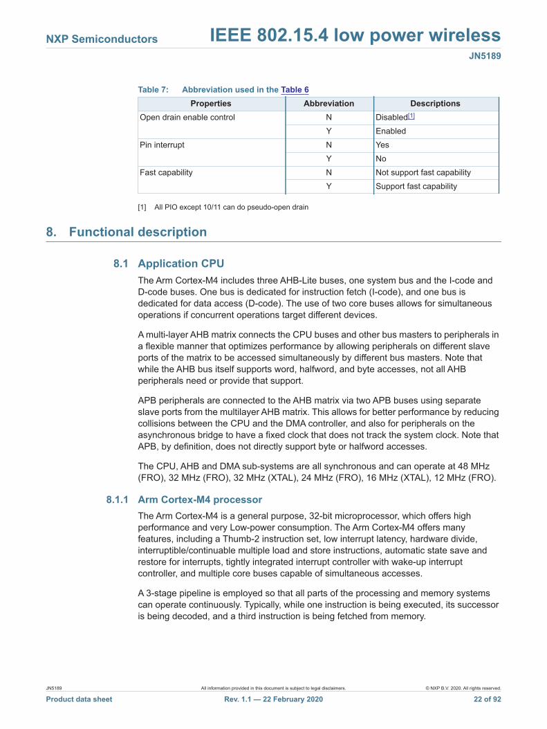
8. Functional description
8.1 Application CPUThe Arm Cortex-M4 includes three AHB-Lite buses, one system bus and the I-code and D-code buses. One bus is dedicated for instruction fetch (I-code), and one bus is dedicated for data access (D-code). The use of two core buses allows for simultaneous operations if concurrent operations target different devices.
A multi-layer AHB matrix connects the CPU buses and other bus masters to peripherals in a flexible manner that optimizes performance by allowing peripherals on different slave ports of the matrix to be accessed simultaneously by different bus masters. Note that while the AHB bus itself supports word, halfword, and byte accesses, not all AHB peripherals need or provide that support.
APB peripherals are connected to the AHB matrix via two APB buses using separate slave ports from the multilayer AHB matrix. This allows for better performance by reducing collisions between the CPU and the DMA controller, and also for peripherals on the asynchronous bridge to have a fixed clock that does not track the system clock. Note that APB, by definition, does not directly support byte or halfword accesses.
The CPU, AHB and DMA sub-systems are all synchronous and can operate at 48 MHz (FRO), 32 MHz (FRO), 32 MHz (XTAL), 24 MHz (FRO), 16 MHz (XTAL), 12 MHz (FRO).
8.1.1 Arm Cortex-M4 processorThe Arm Cortex-M4 is a general purpose, 32-bit microprocessor, which offers high performance and very Low-power consumption. The Arm Cortex-M4 offers many features, including a Thumb-2 instruction set, low interrupt latency, hardware divide, interruptible/continuable multiple load and store instructions, automatic state save and restore for interrupts, tightly integrated interrupt controller with wake-up interrupt controller, and multiple core buses capable of simultaneous accesses.
A 3-stage pipeline is employed so that all parts of the processing and memory systems can operate continuously. Typically, while one instruction is being executed, its successor is being decoded, and a third instruction is being fetched from memory.
Open drain enable control N Disabled[1]
Y EnabledPin interrupt N Yes
Y NoFast capability N Not support fast capability
Y Support fast capability
Table 7: Abbreviation used in the Table 6Properties Abbreviation Descriptions
JN5189 All information provided in this document is subject to legal disclaimers. © NXP B.V. 2020. All rights reserved.
Product data sheet Rev. 1.1 — 22 February 2020 22 of 92
NXP Semiconductors IEEE 802.15.4 low power wirelessJN5189
8.1.2 Memory Protection UnitThe Cortex-M4 includes a Memory Protection Unit (MPU) which can be used to improve the reliability of an embedded system by protecting critical data within the user application.
The MPU allows separating processing tasks by disallowing access to each other's data. Access to memory regions can be disabled and also be defined as read-only. It detects unexpected memory accesses that could potentially break the system.
The MPU separates the memory into distinct regions and implements protection by preventing disallowed accesses. The MPU supports up to eight regions, each of which is divided into eight sub-regions. Accesses to memory locations that are not defined in the MPU regions, or not permitted by the region setting, will trigger memory management fault exception.
8.1.3 System Tick Timer (SysTick)The Arm Cortex-M4 core includes a System Tick timer (SysTick) that generates adedicated SYSTICK exception. The clock source for the SysTick can be the system clock, or a divided version of this.
8.1.4 Nested Vector Interrupt controller (NVIC)The NVIC is an integral part of the Cortex-M4 that efficiently supports many interrupt sources with configurable priority levels.
8.1.4.1 Features
• Nested Vectored Interrupt Controller that is an integral part of the CPU• Tightly coupled interrupt controller provides low interrupt latency• Controls system exceptions and peripheral interrupts• 56 vectored interrupts• 8 programmable interrupt priority levels with hardware priority level masking• Relocatable vector table using Vector Table Offset Register VTOR• Software interrupt generation• Support for Non-Maskable Interrupt (NMI) from any interrupt
8.1.4.2 General descriptionThe tight coupling of the NVIC to the CPU allows for low interrupt latency and efficient processing of late arriving interrupts.
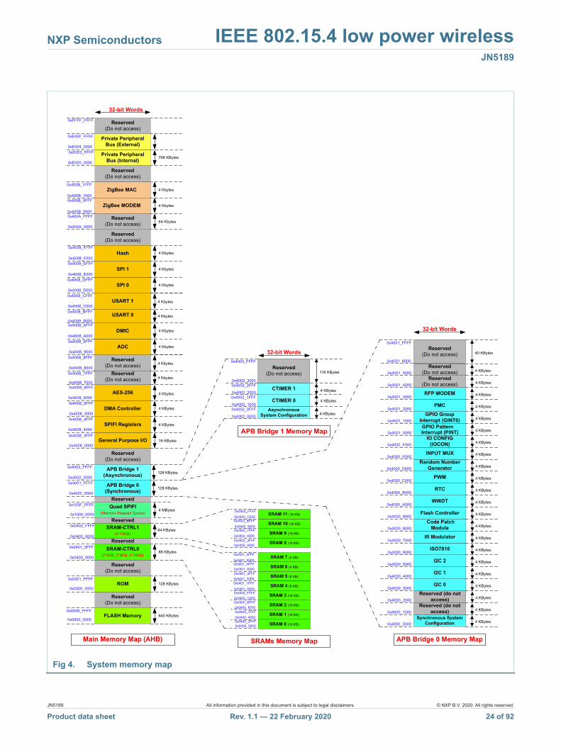
8.2 MemoryThe JN5189 incorporates several distinct memory regions.
The registers incorporated into the CPU, such as NVIC, SysTick, and sleep mode control, are located on the private peripheral bus.
The system memory map is shown in
JN5189 All information provided in this document is subject to legal disclaimers. © NXP B.V. 2020. All rights reserved.
Product data sheet Rev. 1.1 — 22 February 2020 23 of 92
NXP Semiconductors IEEE 802.15.4 low power wirelessJN5189
Fig 4. System memory map
FLASH Memory
Reserved(Do not access)
0x0000_0000
0x0301_FFFF
0x4000_0000
640 KBytes
APB Bridge 0 (Synchronous)
0xFFFF_FFFF
General Purpose I/O
Synchronous System Configuration
ROM
0x0009_FFFF
0x0300_0000
Main Memory Map (AHB) APB Bridge 0 Memory Map
32-bit Words
32-bit Words
Reserved(Do not access)
SRAM-CTRL0(2*4KB, 2*8KB, 4*16KB)0x0400_0000
0x0401_5FFFReserved
Quad SPIFI (Memory-Mapped Space)0x1000_0000
0x103F_FFFFReserved
Reserved(Do not access)
0x4001_FFFF
0x4008_0000
0x4008_3FFF
SPIFI Registers
DMA Controller
AES-256
Reserved(Do not access)
Private Peripheral Bus (Internal)
Private Peripheral Bus (External)
Reserved(Do not access)
0x4008_4FFF
0x4008_5FFF
0x4008_6FFF
0x4008_4000
0x4008_5000
0x4008_6000
0xE003_FFFF
0xE00F_FFFF
0xE004_0000
0xE000_0000
128 KBytes
88 KBytes
4 MBytes
4 KBytes
768 KBytes
16 KBytes
4 KBytes
128 KBytes
4 KBytes0x4000_0000
Reserved (do not access) 4 KBytes0x4000_1000
Reserved (do not access) 4 KBytes0x4000_2000
I2C 0 4 KBytes0x4000_3000
I2C 1 4 KBytes0x4000_4000
I2C 2 4 KBytes0x4000_5000
ISO7816 4 KBytes0x4000_6000
IR Modulator 4 KBytes0x4000_7000
Code Patch Module 4 KBytes0x4000_8000
Flash Controller 4 KBytes0x4000_9000
WWDT 4 KBytes0x4000_A000
RTC 4 KBytes0x4000_B000
PWM 4 KBytes0x4000_C000
4 KBytes0x4000_D000Random Number
Generator
4 KBytes0x4000_E000INPUT MUX
4 KBytes0x4000_F000IO CONFIG
(IOCON)
4 KBytes0x4001_0000
Interrupt (PINT)
4 KBytes0x4001_1000
CTIMER 04 KBytes0x4001_2000
RFP MODEM 4 KBytes0x4001_3000
Reserved(Do not access) 4 KBytes0x4001_4000
Reserved(Do not access)
0x4001_5000
40 KBytes
GPIO Group Interrupt (GINT0)
APB Bridge 1 (Asynchronous)0x4002_0000
0x4003_FFFF
CTIMER 1
APB Bridge 1 Memory Map
4 KBytes0x4002_0000
Reserved(Do not access) 116 KBytes
0x4002_1000
SRAM 0 (16 KB)
SRAMs Memory Map
0x0400_0000
SRAM 1 (16 KB)0x0400_4000
SRAM 2 (16 KB)0x0400_8000
SRAM 5 (8 KB)
0x0400_C000
0x0401_4000
128 KBytes
0x4003_FFFF
0x4002_0FFF
0x4001_FFFF
32-bit Words
PMC
4 Kbytes
Asynchronous System Configuration
0x4002_1FFF0x4002_2000
0x4002_2FFF0x4002_3000
4 KBytes
4 KBytes
SRAM 6 (4 KB)
SRAM 7 (4 KB)
SRAM 8 (16 KB)
SRAM 9 (16 KB)
0x0401_5000
0x0402_0000
0x0402_4000
0x0401_5FFF
0x0402_3FFF
0x0401_4FFF
0x0401_3FFF
0x0400_BFFF
0x0400_7FFF
0x0400_3FFF
0x0402_7FFF
Reserved(Do not access)
ZigBee MODEM
ZigBee MAC
0x400A_0000
0x400B_0000
0x400B_1000
0x400A_FFFF
0x400B_0FFF
0x400B_1FFF4 Kbytes
4 Kbytes
64 Kbytes
Reserved(Do not access)
Reserved(Do not access)
4 Kbytes
4 Kbytes0x4008_8FFF
0x4008_7FFF
0x4008_7000
0x4008_8000
Reserved(Do not access)
0x4008_9000ADC 4 Kbytes
0x4008_9FFF
DMIC 4 Kbytes0x4008_A000
0x4008_AFFF
USART 0
USART 1
4 Kbytes
4 Kbytes0x4008_CFFF
0x4008_BFFF
0x4008_B000
0x4008_C000
0x4008_D000SPI 0 4 Kbytes
0x4008_DFFF
SPI 1 4 Kbytes0x4008_E000
0x4008_EFFF
SRAM 3 (16 KB)
SRAM 4 (8 KB)
0x0400_FFFF0x0401_0000
0x0401_20000x0401_1FFF
SRAM-CTRL1(4*16KB)
64 KBytes0x0402_0000
0x0402_FFFFReserved
SRAM 10 (16 KB)
SRAM 11 (16 KB)
0x0402_8000
0x0402_FFFF0x0402_C0000x0402_BFFF
Reserved(Do not access) 4 KBytes
0x4001_6000
Hash 4 Kbytes0x4008_F000
0x4008_FFFF
GPIO Pattern
JN5189 All information provided in this document is subject to legal disclaimers. © NXP B.V. 2020. All rights reserved.
Product data sheet Rev. 1.1 — 22 February 2020 24 of 92
NXP Semiconductors IEEE 802.15.4 low power wirelessJN5189
8.2.1 SRAMThe main SRAM is comprised of up to a total 152 KB on-chip static RAM memory. The main SRAM is implemented as several SRAM instances to allow for more control of power usage when less SRAM is required (2 4 KB instances, 2 8 KB instances and 8 16 KB instances). Each SRAM has a separate clock control and power switch.
See Table 2 for SRAM size of each parts.
8.2.2 SRAM usageAlthough always contiguous on all JN5189 devices, the SRAM instances are divided between two AHB matrix ports. This allows user programs to potentially obtain better performance by dividing RAM usage among the ports. For example, simultaneous access to SRAM0 by the CPU and SRAM1 by the system DMA controller does not result in any bus stalls for either master.
Generally speaking, the CPU will read or write all peripheral data at some point, even when all such data is read from or sent to a peripheral by DMA. So, minimizing stalls is likely to involve putting data to/from different peripherals in RAM on each port.
Alternatively, sequences of data from the same peripheral could be alternated between RAM on each port. This could be helpful if DMA fills or empties a RAM buffer, then signals the CPU before proceeding on to a second buffer. The CPU would then tend to access the data while the DMA is using RAM on the other port. On the JN5188, all the RAM is accessed through one AHB matrix slave port.
8.2.3 FLASHThe JN5189 embeds flash for code and data storage. It is accessed through a flash controller that simplifies the use of the flash.
• JN5189 embeds a total of 640 KB of Flash, JN5188 a total of 320 KB• Flash sector is 512 bytes• 100 kcycles page endurance guaranteed• Software is provided to manage data storage in the flash and provides wear leveling
features• Data retention 10 years
8.2.4 AHB multilayer matrixThe JN5189 uses a multi-layer AHB matrix to connect the CPU buses and other bus masters to peripherals in a flexible manner that optimizes performance by allowing peripherals that are on different slave ports of the matrix to be accessed simultaneously by different bus masters.
8.3 System clocksThe following system clocks are used to drive the on-chip subsystems of the JN5189:
• The low power wake timers are driven by a low frequency 32 kHz clock.• The main digital systems are driven from a high frequency clock source.• The system controller state machines are driven from a 1 MHz FRO.
JN5189 All information provided in this document is subject to legal disclaimers. © NXP B.V. 2020. All rights reserved.
Product data sheet Rev. 1.1 — 22 February 2020 25 of 92
NXP Semiconductors IEEE 802.15.4 low power wirelessJN5189
These system clocks are used within the device for the digital functionality. Some functional blocks can also source a clock from the interface and this is explained in when the digital blocks are presented.
8.3.1 32 kHz clockThere are two possible sources for the 32kHz clock.
There is an internal FRO that gives 32.768 kHz with accuracy of +/-2%; this requires no external components.
A 32 kHz XTAL is also supported. The XTAL is connected to XTAL_32K_P and XTAL_32K_N pins. The cell has configurable internal capacitors and therefore, except for the XTAL itself, no other external components are typically required. Very accurate XTALs are available. This option is recommended for accurate timings.
8.3.2 High frequency system clockThere are two possible sources for the high-speed system clock.
There is an internal high speed FRO that supports clock frequencies of 48 MHz, 32 MHz, 24 MHz and 12 MHz. This does not require any external components and has an accuracy of ±2%.
A 32 MHz XTAL is also supported. The cell has configurable internal capacitors and therefore, except for the XTAL itself, no other external components are typically required. An accurate XTAL must be used for the radio operation. The system clock can be chosen to be sourced from the FRO or XTAL and this choice is separate to the operation of the radio using the XTAL clock. When selecting the XTAL as the source for the high frequency system clock, it is possible to select 32 MHz or 16 MHz.
The high frequency system clock is used for the processor and the system buses.
8.3.3 1 MHz FROA 1 MHz FRO is used by the core system controller and the state machine involved in the device start-up and shut-down. High accuracy of this clock is not necessary and it has a tolerance of 15%.
8.4 Resets and brownoutA system reset initializes the device to a pre-defined state and forces the CPU to start program execution from the reset vector. The reset process that the JN5189 goes through is as follows.
When power is first applied or when the external reset is released, the FRO1MHz is started, then the DCDC converter is started. After that, the system power domain is started. When these domains are stable, the flash and main core domain LDOs are enabled. When these are stable, the high speed FRO is enabled and the elements necessary for CPU operation are enabled. Configuration data is read from the flash and the boot process begins.
Depending on the configuration and flash contents then the application may be executed, or the device may enter In System Programming (ISP) mode.
JN5189 All information provided in this document is subject to legal disclaimers. © NXP B.V. 2020. All rights reserved.
Product data sheet Rev. 1.1 — 22 February 2020 26 of 92
NXP Semiconductors IEEE 802.15.4 low power wirelessJN5189
The initial power-up sequence will not begin if the device power is too low; in this case the Power-on reset module will keep the device in a reset state until there is sufficient voltage. Additionally, the brown-out detect block will keep the device in reset until a safe operating voltage is reached.
Once the device is operating, the brownout module can be used to interrupt the processor in case operating voltage changes occur. This allows software to manage a clean response to the event. The brownout threshold is configurable to support a range of applications.
Several resets are supported that can affect all or most of the device. These are presented in the following sub-sections.
8.4.1 External resetAn external reset is generated by a low level on the RSTIN pin. Reset pulses longer than the minimum pulse width will generate a reset during active or power-down modes. Shorter pulses are not guaranteed to generate a reset. The JN5189 is held in reset while the RSTIN pin is low. When the applied signal reaches the reset threshold voltage on its positive edge, the internal reset process starts.
The JN5189 has an internal pull-up resistor connect to the RSTIN pin. This pin is the input for an external reset only.
8.4.2 Software resetA system reset can be triggered at any time through software control, causing a full chip reset and invalidating the RAM contents. For example, this can be executed within a user's application upon detection of a system failure.
8.4.3 Watchdog timerThe watchdog timer can cause a full chip reset if it reaches its timeout point and it is configured to generate a reset, rather than an interrupt. In normal operation, the software will periodically service the watchdog to prevent this timeout occurring. Typically, a watchdog timeout indicates an unexpected lock-up within the system.
8.4.4 Arm system resetThe CPU can cause a reset by requesting a System reset. This reset causes a reset of the CPU and the core digital functionality, digital peripherals and the 32 MHz XTAL. The power domains within the device, such as the DCDC converter and core LDO are unaffected so that the CPU will restart quicker than if a software reset is performed.
8.5 System configuration (SYSCON)The device has many system level features which support the operation of the device, such as clock control. In addition there is functionality provided to allow the software to manage the system, such as controlling wake-up sources. These features include:
• System and bus configuration• Clock select and control• Reset control• Wake-up control
JN5189 All information provided in this document is subject to legal disclaimers. © NXP B.V. 2020. All rights reserved.
Product data sheet Rev. 1.1 — 22 February 2020 27 of 92

NXP Semiconductors IEEE 802.15.4 low power wirelessJN5189
• Brown-out (BOD) configuration• High-accuracy frequency measurement function for on-chip and off-chip clocks, using
a selection of on-chip clocks as reference clock• Device ID register
8.6 Power managementThis section provides an overview of power related information about JN5189 devices.
These devices include a variety of adjustable regulators, power switches, and clock switches to allow fine tuning power usage to match requirements at different performance levels and reduced power modes. All devices include an on-chip API in the boot ROM to adjust power consumption in reduced power modes, and provide entry to those modes.
8.6.1 Power supplyThe device is powered by VBAT, which requires a 10 F decoupling capacitor to ground.
To give efficient operation, the device has an on-chip DCDC buck converter; it is turned on when the device is in active and sleep modes and, using external connections, it provides the supply voltage to the PMU and Radio. The converter is powered from VBAT and the external output of the DCDC converter, FB, requires a 10 F decoupling capacitor to ground. For the DCDC converter to function correctly, a filtered version of FB must be input to LX, This is achieved with a 4.7 H inductor. The DCDC converter output, FB, must be routed to device pins VDD(radio) and VDD(pmu) so that the whole system is powered correctly.
The two VDD power inputs supply the power to most of the device, either directly or via on-chip regulators and power switches. These are used to manage power consumption based on the required mode of operation.
There is an always-on power domain which is powered by VBAT and includes the core functions to control device start-up and the functionality required in the very low power modes. This domain always has power as long as sufficient voltage is supplied to VBAT.
A further domain is important for supporting the power down mode. It includes the RTC, wake-up timer and some clock, reset and wakeup control. This domain is always has power as long as sufficient voltage is supplied to VDD and provided that the device is not in deep power-down mode.
See Figure 10 “Application diagram – battery powered solution” for the power connections.
8.6.2 Power modesA variety of power modes are supported for the optimization of power consumption, including active, sleep, deep-sleep, power-down and deep power-down. Upon power-up or reset, the device enters active mode. After processing is complete, the software puts the chip into sleep mode or power-down mode, to save power consumption. The device is woken up either by a reset or an interrupt trigger like a GPIO interrupt, timer timeout, or other wake-up sources.
JN5189 All information provided in this document is subject to legal disclaimers. © NXP B.V. 2020. All rights reserved.
Product data sheet Rev. 1.1 — 22 February 2020 28 of 92
NXP Semiconductors IEEE 802.15.4 low power wirelessJN5189
An API is provided so that software can easily use the power modes. The API performs all the configuration necessary for the different power modes, including setting power domains to the correct state and voltage, shutting down the flash controller safely, enabling the wake up mechanisms. The following sections introduces modes supported in order from highest to lowest power consumption.
8.6.2.1 Active modeThe part is in active mode after a Power-On Reset (POR) and when it is fully powered and operational after booting.
8.6.2.2 Sleep modeSleep mode saves a significant amount of power by stopping CPU execution without affecting peripherals or requiring significant wake-up time. The sleep mode affects the relevant CPU only. The clock to the core is shut off. Peripherals and memories are active and operational.
8.6.2.3 Deep-sleep modeDeep-sleep mode is highly configurable and can reduce power consumption, compared to Sleep mode by turning off more functions. Additionally, core voltages are reduced to save power. Wake-up times are longer than for Sleep mode due to the time needed to restart the functions. The clock to both CPUs is shut down. The clock to the peripherals may also be disabled. The SRAM and registers maintain their internal states.
Entry to these modes can be accomplished by the CPU using the power profiles API, selected peripherals can be left running for safe operation of the part (e.g. RTC, WWDT and BOD, depending upon the mode). The flash is placed in standby mode and system clocks may be disabled.
8.6.2.4 Power-down modeIn Power-down mode the core of the device and the flash is powered down, most clocks are stopped. Power consumption is very low with the cost of a longer wake-up time. The processor and most digital peripherals are powered off. USART0, SPI0 and I2C0 can operate with limited functionality in power down mode and have the ability to wake the device. Low power sleep timers can be enabled to generate a wake-up at a certain time in the future. Wakeup is also possible by GPIOs, analog comparator, RTC, BOD VBAT and NTAG field detect. All, of part, of the SRAM can be optionally retained at the cost of extra current consumption.
8.6.2.5 Deep power-down modeDeep Power-down mode shuts down virtually all on-chip power consumption, but requires a significantly longer wake-up time. For maximal power savings, the entire system (CPUs, memories and all peripherals) is shut down except for the PMU. Wake-up is possible from reset, NTAG field detect, and optionally GPIO. On wake-up, the part reboots.
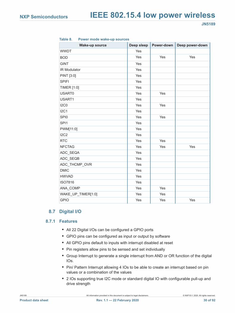
8.6.2.6 Wake-up sourcesAll interrupts to the CPU can be used as a wake-up from sleep.
The following table shows the possible wake-up sources from deep-sleep, power-down and deep power-down.
JN5189 All information provided in this document is subject to legal disclaimers. © NXP B.V. 2020. All rights reserved.
Product data sheet Rev. 1.1 — 22 February 2020 29 of 92
NXP Semiconductors IEEE 802.15.4 low power wirelessJN5189
8.7 Digital I/O
8.7.1 Features
• All 22 Digital I/Os can be configured a GPIO ports• GPIO pins can be configured as input or output by software• All GPIO pins default to inputs with interrupt disabled at reset• Pin registers allow pins to be sensed and set individually• Group Interrupt to generate a single interrupt from AND or OR function of the digital
IOs.• Pin/ Pattern Interrupt allowing 4 IOs to be able to create an interrupt based on pin
values or a combination of the values• 2 IOs supporting true I2C mode or standard digital IO with configurable pull-up and
drive strength
Table 8. Power mode wake-up sourcesWake-up source Deep sleep Power-down Deep power-down
WWDT Yes
BOD Yes Yes Yes
GINT YesIR Modulator YesPINT [3:0] YesSPIFI YesTIMER [1:0] YesUSART0 Yes YesUSART1 YesI2C0 Yes YesI2C1 YesSPI0 Yes YesSPI1 YesPWM[11:0] YesI2C2 YesRTC Yes YesNFCTAG Yes Yes YesADC_SEQA YesADC_SEQB YesADC_THCMP_OVR YesDMIC YesHWVAD YesISO7816 YesANA_COMP Yes YesWAKE_UP_TIMER[1:0] Yes YesGPIO Yes Yes Yes
JN5189 All information provided in this document is subject to legal disclaimers. © NXP B.V. 2020. All rights reserved.
Product data sheet Rev. 1.1 — 22 February 2020 30 of 92

NXP Semiconductors IEEE 802.15.4 low power wirelessJN5189
• 20 standard IO cells configurable for drive strength, pull-up resistor, pull-down resistor, pseudo open-drain
8.7.2 General descriptionThe 22 digital IOs have multiplexed functionality, supporting one or more digital peripherals and also a basic General Purpose IO function (GPIO). In GPIO mode it is possible to configure the IO as an input or as an output.
As an input it is possible to configure IO wake a device from powerdown and deep powerdown. The input value can also be read.
Using the Pin Interrupt/ Pattern Match function (PINT) it is possible to configure up to 4 digital IOs to be able to generate an interrupt based for active high or low functionality. Alternatively the 4 IOs can be combined in various ways to generate an interrupt. These interrupt are able to wake the CPU from sleep mode.
Additionally, a Group Interrupt function (GINT) allows any selection of upto all 22 IOs to be combined into a AND or OR function in order to generate the group interrupt. The polarity of each IO used in the function can be configured.
Two of the digital IO cells support true I2C functionality and standard digital IO functionality, These support a pull-up resistor, drive strength control.
The other 20 digital IOs cells are configurable to support drive strength options, pull-up or pull-down functions and the ability to operate in a pseudo open-drain mode.
The output value of each IO can be held during a power-down cycle if required.
8.8 DMA controllerThe DMA controller allows peripheral to memory, memory to peripheral, and memory single source and destination.
• 19 channels which are connected to peripheral DMA requests. These come from the USART, SPI-bus, I2C-bus, PDM and SPIFI interfaces. Any otherwise unused channels can also be used for functions such as memory-to-memory moves.
• DMA operations can be triggered by on-chip or off-chip events. Each DMA channel can select one trigger input from 18 sources. Trigger sources include ADC interrupts, timer interrupts, pin interrupts, and the SCT DMA request lines
• Priority is user selectable for each channel (up to eight priority levels)• Continuous priority arbitration• Address cache with four entries (each entry is a pair of addresses)• Efficient use of data bus• Supports single transfers up to 1,024 words• Address increment options allow packing and/or unpacking data
8.9 PWMThe PWM module supports the generation of up to 10 PWM waveforms, each with its own prescaler, to support a range of applications.
• 1 PWM module with 10 independent outputs
JN5189 All information provided in this document is subject to legal disclaimers. © NXP B.V. 2020. All rights reserved.Product data sheet Rev. 1.1 — 22 February 2020 31 of 92
NXP Semiconductors IEEE 802.15.4 low power wirelessJN5189
• Option for 1 channel to drive up to 1 channel driving the 10 outputs simultaneously• Programmable 10-bit prescaler for eac.h channel• 16-bit auto-reload down counter for each channel• 16-bit compare register for each channel (toggling point in 1 full period)• Predictable PWM initial output state for each channel (configurable initial waveform
polarity – HIGH or LOW)• Configurable level (HIGH or LOW) of PWM output when PWM is disabled• Programmable overflow interrupt generation for each channel
8.10 TimersWithin the JN5189 there are several different timer blocks available. These timers are used in different ways as outlined here.
• Counter/Timers: The two blocks are the main functional timers for the application, running off a high speed clock and able to create interrupts from match registers.
• Watchdog Timer: slow speed timer with the ability to interrupt the processor or cause device reset. Often used to identify when application software is locked up or taking too long.
• Real-time clock: this block has two timers real time clock and high-resolution/wake-up timer. The real time clock has a 1Hz clock is often run continually as a clock. The high-resolution/ wake up timer is a simple counter that can generate an input to wake the device from sleep, deep-sleep and power-down. Maximum timeout is 64 seconds.
• Low Power Wake-up Timers: this block has two timers running on a 32kHz. Predominantly used to wake the device from power-down, with a maximum time period in excess of one year.
• Tick Timer: within the processor this is often used for a regular heart beat to trigger software scheduling.
The device has different power modes and the following table shows when the timers can be used.
8.10.1 Counter/TimersThere are two Counter/Timer blocks that support a range of functions such as timers or counting events from an IO pin. The match registers allow for configurable interrupts when the counter reaches certain values. The match events can also be indicated on device pins.
Table 9. Allowed timer usage in different power modesTimer block Active mode Sleep mode Deep-sleep
modePower-down
modeDeep power-down
modeCounter/timer X X XWatchdog timer X X XReal-time clock X X X XLow Power wake-up timers X X X XTick timer X X X
JN5189 All information provided in this document is subject to legal disclaimers. © NXP B.V. 2020. All rights reserved.
Product data sheet Rev. 1.1 — 22 February 2020 32 of 92
NXP Semiconductors IEEE 802.15.4 low power wirelessJN5189
8.10.1.1 Features
• 2 counter/timer instances, CT32B0 and CT32B1• Each is a 32-bit counter/timer with a programmable 32-bit prescaler. Both timers
include external capture and match pin connections• Counter or timer operation• For each timer, up to 2 32-bit capture channels that can take a snapshot of the timer
value when an input signal transitions. A capture event may also optionally generate an interrupt
• The timer and prescaler may be configured to be cleared on a designated capture event. This feature permits easy pulse-width measurement by clearing the timer on the leading edge of an input pulse and capturing the timer value on the trailing edge
• Four 32-bit match registers that allow:– Continuous operation with optional interrupt generation on match– Stop timer on match with optional interrupt generation– Reset timer on match with optional interrupt generation
• For each timer with pin connections, up to 2 external outputs corresponding to match registers with the following capabilities:– Set LOW on match– Set HIGH on match– Toggle on match– Do nothing on match– Two match registers can be used to trigger DMA transfers.
8.10.1.2 General descriptionEach counter/timer is designed to count cycles of the APB bus clock or an externally supplied clock and can optionally generate interrupts or perform other actions at specified timer values based on four match registers. Each counter/timer also includes one capture input to trap the timer value when an input signal transitions, optionally generating an interrupt.
Capture inputs: The capture signal can be configured to load the capture register with the value in the counter/timer and optionally generate an interrupt. The capture signal is generated by one of the pins with a capture function. Each capture signal is connected to one capture channel of the timer.
The counter/timer block can select a capture signal as a clock source instead of the APB bus clock.
Match outputs: When a match register equals the Timer Counter (TC), the corresponding match output can either toggle, go LOW, go HIGH, or do nothing.
Applications
• Interval timer for counting internal events• Pulse Width Modulator via match outputs• Pulse Width Demodulator via capture input
JN5189 All information provided in this document is subject to legal disclaimers. © NXP B.V. 2020. All rights reserved.
Product data sheet Rev. 1.1 — 22 February 2020 33 of 92
NXP Semiconductors IEEE 802.15.4 low power wirelessJN5189
• Free running timer
8.10.2 Watchdog timerThe purpose of the Watchdog Timer is to reset or interrupt the microcontroller within a programmable time if it enters an erroneous state. When enabled, a watchdog reset is generated if the user program fails to feed (reload) the Watchdog within a predetermined amount of time.
When a watchdog window is programmed, an early watchdog feed is also treated as a watchdog event. This allows preventing situations where a system failure may still feed the watchdog. For example, application code could be stuck in an interrupt service that contains a watchdog feed. Setting the window such that this would result in an early feed will generate a watchdog event, allowing for system recovery.
• Internally resets chip if not reloaded during the programmable time-out period• Optional windowed operation requires reload to occur between a minimum and
maximum time-out period, both programmable• Optional warning interrupt can be generated at a programmable time prior to
watchdog time-out• Clock fed to the watchdog function is selectable from 32 kHz clock, 32 MHz clock and
FRO 1 MHz clock, This selected clock can be optionally pre-scaled before input to the block.
• Programmable 24-bit timer with internal fixed pre-scaler• Selectable time period• “Safe” watchdog operation. Once enabled, requires a hardware reset or a watchdog
reset to be disabled• Incorrect feed sequence causes immediate watchdog event if enabled• The watchdog reload value can optionally be protected such that it can only be
changed after the “warning interrupt” time is reached• Flag to indicate watchdog reset• The watchdog timer can be configured to run in Deep-sleep mode• Debug mode
8.10.3 Real-Time Clock (RTC)The Real-Time Clock provides two timers that are typically used as a Real-Time clock counter and a higher-resolution timer.
8.10.3.1 Features
• The RTC has the following clock inputs generated from the 32 kHz FRO or 32 kHz XTAL:– 1 Hz clock for RTC timing– 1 kHz clock for high-resolution RTC timing
• 32-bit, 1 Hz RTC counter and associated match register for alarm generation• Separate 16-bit high-resolution/wake-up timer clocked at 1 kHz for 1 ms resolution
giving a maximum time-out period of over one minute.
JN5189 All information provided in this document is subject to legal disclaimers. © NXP B.V. 2020. All rights reserved.
Product data sheet Rev. 1.1 — 22 February 2020 34 of 92
NXP Semiconductors IEEE 802.15.4 low power wirelessJN5189
• RTC alarm and high-resolution/wake-up timer time-out each generate independent interrupt requests. Either time-out can wake up the part from Low-power modes (Sleep mode, Deep-sleep mode or Power-down mode)
8.10.3.2 General descriptionThe RTC contains two timers:
• Real time clockThe real-time clock is a 32-bit up-counter which can be cleared or initialized by software. Once enabled, it counts continuously at a 1 Hz clock rate as long as the device is powered up and the RTC remains enabled.The main purpose of the RTC is to count seconds and generate an alarm interrupt to the processor whenever the counter value equals the value programmed into the associated 32-bit match register.If the part is in one of the reduced-power modes (Sleep, Deep-sleep, Power-down) an RTC alarm interrupt can also wake up the part to exit the Power mode and begin normal operation.
• High-resolution/wake-up timerThe time interval required for many applications, including waking the part up from a Low-power mode, will often demand a greater degree of resolution than the one-second minimum interval afforded by the main RTC counter. For these applications, a higher frequency secondary timer has been provided.This secondary timer is an independent, stand-alone wake-up or general-purpose timer for timing intervals of up to 64 seconds with approximately one millisecond of resolution.The high-resolution/wake-up timer is a 16-bit down counter which is clocked at a 1 kHz rate when it is enabled. Writing any non-zero value to this timer will automatically enable the counter and launch a countdown sequence. When the counter is being used as a wake-up timer, this write can occur just prior to entering a reduced power mode. When a starting count value is loaded, the high-resolution/wake-up timer will turn on, count from the pre-loaded value down to zero, generate an interrupt and/or a wake-up command, and then turn itself off until re-launched by a subsequent software write.
8.10.4 Low Power Wake-up TimersTwo low power wake-up timers are available on the JN5189, driven from the 32 kHz internal clock. They may run in power-down mode when the majority of the rest of the device is powered down, to time low-power periods or other long period timings that may be required by the application. The wake-up timers do not run during deep power-down and may optionally be disabled in power-down mode through software control. When a wake-up timer expires, it typically generates an interrupt; if the device is in deep sleep or power down mode then the interrupt may be used as an event to end the low power mode. Features include:
• 28-bit and 41-bit down counter• Optionally runs during power-down periods• Clocked by 32 kHz system clock; either 32 kHz RC oscillator, or 32 kHz XTAL
oscillator
JN5189 All information provided in this document is subject to legal disclaimers. © NXP B.V. 2020. All rights reserved.
Product data sheet Rev. 1.1 — 22 February 2020 35 of 92
NXP Semiconductors IEEE 802.15.4 low power wirelessJN5189
• Time-out period in excess of 1 year is possible
A wake-up timer consists of a 28-bit or 41-bit down counter clocked from the selected 32 kHz clock. An interrupt or wake-up event can be generated when the counter reaches zero. On reaching zero, the counter will continue to count down until stopped, which allows the latency in responding to the interrupt to be measured. If an interrupt or wake-up event is required, the timer interrupt should be enabled before loading the count value for the period. Once the counter value has been loaded and the counter started, the count-down begins. The counter can be stopped at any time through software control - the counter will remain at the value that it contained when it was stopped and no interrupt will be generated. The status of the timers can be read to indicate if the timers are running and/or have expired; this is useful when the timer interrupts are masked.
8.11 USARTThere are 2 USART interfaces to provide Synchronous and Asynchronous serial communications with external devices. A range of features and flexible baud rate control supports a range of applications.
• 2 USART interfaces, 1 with flow control• 7, 8 or 9 data bits and 1 or 2 stop bits• Synchronous mode with master or slave operation. Includes data phase selection and
continuous clock option• Multiprocessor/multidrop (9-bit) mode with software address compare• RS-485 transceiver output enable• Parity generation and checking: odd, even, or none• Software selectable oversampling from 5 to 16 clocks in asynchronous mode• One transmit and one receive data buffer• The USART function supports separate transmit and receive FIFO with 4 entries each• RTS/CTS supported on one USART. This allows for hardware signaling for automatic
flow control. Software flow control can be performed using delta CTS detect, transmit disable control, and any GPIO as an RTS output
• Break generation and detection• Receive data is 2 of 3 sample "voting". status flag set when one sample differs• Built-in baud rate generator with auto-baud function• A fractional rate divider is shared among all USARTs• Interrupts available for FIFO receive level reached, FIFO transmit level reached,
receiver idle, change in receiver break detect, framing error, parity error, overrun, underrun, delta CTS detect, and receiver sample noise detected
• Loopback mode for testing of data and flow control• USART transmit and receive functions can operate with the system DMA controller• Special operating mode allows operation at up to 9600 baud using the 32 kHz RTC
oscillator as the USART clock. This mode can be used, with USART0, while the device is in Power-down mode and can wake-up the device when a character is received
JN5189 All information provided in this document is subject to legal disclaimers. © NXP B.V. 2020. All rights reserved.
Product data sheet Rev. 1.1 — 22 February 2020 36 of 92
NXP Semiconductors IEEE 802.15.4 low power wirelessJN5189
8.12 Serial Peripheral Interfaces-bus (SPI-bus)The SPI-bus allows high-speed synchronous data transfer between the JN5189 and peripheral devices. Two SPI-buses are supported which can independently operate as a master or slave to support a range of system configurations.
• 2 SPI-bus interfaces: SPI0 and SPI1 can be both configured as master or slave interfaces
• Data transmits of 1 to 16 bits supported directly. Larger frames supported by software• The SPI-bus function supports separate transmit and receive FIFOs with 4 16-bit
entries each• Supports DMA transfers: SPIn transmit and receive functions can operate with the
system DMA controller• Data can be transmitted to a slave without the need to read incoming data. This can
be useful while setting up an SPI-bus memory• Up to 3 slave select input/outputs with selectable polarity and flexible usage
Remark: Texas Instruments SSI and National Microwire modes are not supported.
8.13 I2C-bus interfacesThe JN5189 supports the industry standard I2C-bus, a 2-wire synchronous serial interface that can operate as a master or slave, providing a simple and efficient method of data exchange between devices. The system uses serial data and clock to perform bidirectional data transfers.
• 2 I2C-bus interfaces, one with I2C compliant IO cells• Independent master, slave and monitor functions• Bus speeds supported:
– Standard mode, up to 100 kbits/s– Fast-mode, up to 400 kbits/s– Fast-mode Plus, up to 1 Mbits/s (on specific I2C-bus pins)– High speed mode, 3.4 Mbits/s as a slave only (on specific I2C-bus pins)
• Supports both multi-master and multi-master with slave functions• Multiple I2C-bus slave addresses supported in hardware• One slave address can be selectively qualified with a bit mask or an address range in
order to respond to multiple I2C-bus addresses• 10-bit addressing supported with software assist• Supports System Management Bus (SMBus)• Separate DMA requests for master, slave, and monitor functions• No chip clocks are required in order to receive and compare an address as a slave, so
this event can wake up the device from Power-down mode with I2C0• Automatic modes optionally allow less software overhead for some use cases
JN5189 All information provided in this document is subject to legal disclaimers. © NXP B.V. 2020. All rights reserved.
Product data sheet Rev. 1.1 — 22 February 2020 37 of 92
NXP Semiconductors IEEE 802.15.4 low power wirelessJN5189
8.14 DMIC interfaceThe DMIC subsystem supports mono or dual-channel digital PDM microphones Additionally, hardware voice activity detector (HWVAD), is provided to support low power voice applications.
• DMIC (dual/stereo digital microphone interface)– PDM (Pulse-Density Modulation) data input for left and/or right channels on 1 or 2
buses.– Flexible decimation.– 16 entry FIFO for each channel.– DC blocking or unaltered DC bias can be selected.– Data can be transferred using DMA
• HWVAD (Hardware-based voice activity detector):– Optimized for PCM signals with 16 kHz sampling frequency.– Configurable detection levels.– Noise envelope estimator register output for further software analysis
8.15 12-bit general purpose ADCThe JN5189 has a 12-bit, multi-channel, general purpose ADC. Sampling is controlled by a configurable sequencer that can support a range of sampling options. With connections to the DMA sub-system complex applications using the ADC are possible.
• Conversion rate 100 ksamples/s for 12-bit resolution• Single-ended analog input mode• 8 input channels, (6 external, 1 internal temperature sensor, 1 internal supply voltage
monitoring)• Selectable (max 32 clock-cycles) sampling time• Power-down mode performing minimal power dissipation• Peak to peak single-ended input range from 0 V to 3.6 V• INL (Integral Non Linearity), full scale: 1.1 LSB typ.• DNL (Differential Non Linearity): 0.85 LSB max.• ENOB (Effective Number Of Bit), 10% - 90% full scale, Fin = 25 kHz: 10.5 typ.• SNR (Signal to Noise Ratio), Fin = 25 kHz: 65 dB typ.• THD (Total Harmonic Distortion), 10% - 90% full scale, Fin = 25 kHz: 70 dB typ.• SFDR (Spurious Free Dynamic Range), 10% - 90% full scale, Fin = 25 kHz: 75 dB typ.• A sequencer to control use of ADC
– Sequencer triggered by software or PINT function, or PWM signal– Sample any combination of the 8 ADC channels– Digital comparator function with two pairs of configurable low and high thresholds– Associate each ADC channel to one pair of low/high thresholds– Single step and bursts – Interrupts for data available, data overrun, threshold events
JN5189 All information provided in this document is subject to legal disclaimers. © NXP B.V. 2020. All rights reserved.
Product data sheet Rev. 1.1 — 22 February 2020 38 of 92
NXP Semiconductors IEEE 802.15.4 low power wirelessJN5189
8.16 Temperature sensorThe JN5189 provides a temperature sensor which is connected to one of the ADC channels. It provides an application with a temperature measurement.
• calibrated to give accurate measurement• simple to use with software driver
8.17 Analog comparatorThe JN5189 provides an analog comparator that can compare two device pins or one pin against an internal reference.
• 1 analog comparator with 2 external inputs• The negative source of the comparator can be set to an internal bandgap reference• Can be enabled/disabled to save power• Can be used to wake-up the device, from sleep, deep-sleep or power-down• Rail to rail inputs• The comparator provides 2 power modes to compromise between speed and power
consumption• The external pins can be routed to the + or inputs of the comparator• Hysteresis can be set to 0 mV or 40 mV• The comparator output can be routed to an GPIO
8.18 Infra-Red ModulatorThe Infra-red modulator can generate patterns suitable to drive an infra-red source, The modulator is configurable to support several different IR protocols.
• 1 Infra-Red modulator instance• Support Phillips RC5, RC6 & RCMM protocols• Support SONY SIRC protocol• Support 36 kHz sub-carrier frequency• Support 40 kHz sub-carrier frequency
8.19 Serial Wire Debug (SWD)Debug and trace functions are integrated into the Arm Cortex-M4. Serial wire debug and trace functions are supported. The Arm Cortex-M4 is configured to support up to 8 breakpoints and 4 watch points.
8.19.1 Features
• Supports Arm Serial Wire Debug mode for Cortex-M4• Trace port provides Cortex-M4 CPU instruction trace capability. Output via a serial
wire viewer• Direct debug access to all memories, registers, and peripherals• No target resources are required for the debugging session
JN5189 All information provided in this document is subject to legal disclaimers. © NXP B.V. 2020. All rights reserved.
Product data sheet Rev. 1.1 — 22 February 2020 39 of 92
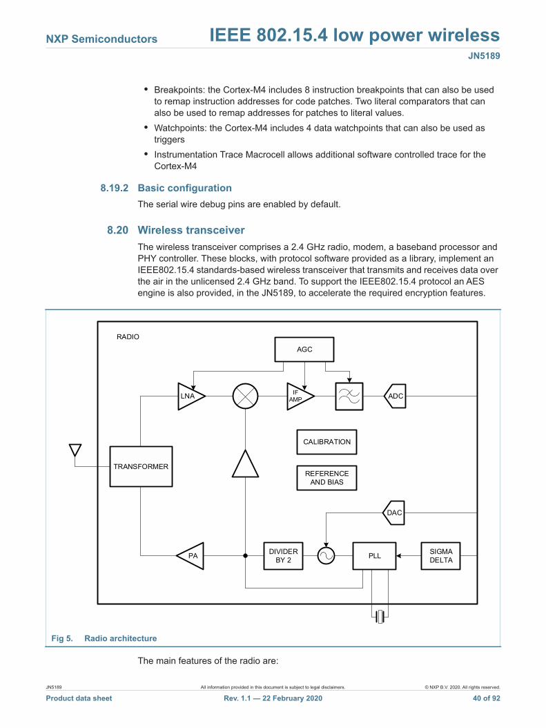
NXP Semiconductors IEEE 802.15.4 low power wirelessJN5189
• Breakpoints: the Cortex-M4 includes 8 instruction breakpoints that can also be used to remap instruction addresses for code patches. Two literal comparators that can also be used to remap addresses for patches to literal values.
• Watchpoints: the Cortex-M4 includes 4 data watchpoints that can also be used as triggers
• Instrumentation Trace Macrocell allows additional software controlled trace for the Cortex-M4
8.19.2 Basic configurationThe serial wire debug pins are enabled by default.
8.20 Wireless transceiverThe wireless transceiver comprises a 2.4 GHz radio, modem, a baseband processor and PHY controller. These blocks, with protocol software provided as a library, implement an IEEE802.15.4 standards-based wireless transceiver that transmits and receives data over the air in the unlicensed 2.4 GHz band. To support the IEEE802.15.4 protocol an AES engine is also provided, in the JN5189, to accelerate the required encryption features.
The main features of the radio are:
Fig 5. Radio architecture
CALIBRATION
PA
RADIO
ADC
TRANSFORMERREFERENCE
AND BIAS
PLL SIGMA DELTA
AGC
DIVIDER BY 2
LNA IF AMP
DAC
JN5189 All information provided in this document is subject to legal disclaimers. © NXP B.V. 2020. All rights reserved.
Product data sheet Rev. 1.1 — 22 February 2020 40 of 92
NXP Semiconductors IEEE 802.15.4 low power wirelessJN5189
• Single ended shared RF input for receive and transmit operations• Each power domain has its own independent LDO• A low noise PLL serving either the receiver or the transmitter. A 2-point modulation is
used in TX
The single-ended antenna is connected to the integrated transformer. The integrated transformer has 2 outputs, one for the receive chain one for the TX chain.
The RX chain consists in an LNA, a mixer, an IF amplifier, an anti-aliasing filter and an ADC.
The LNA has some gain steps that are controlled by the AGC system.
The IF amplifier is the first gain stage after the mixer and provides some filtering. It has some gain steps that are controlled by the AGC system.
The anti-aliasing filter is the main channel filter. It also provides some gain steps that are controlled by the AGC system.
On the transmit side, the PA is built as 2 main blocks: one containing the RF pre-driver, one containing the power amplifier. The power amplifier has its own high power LDO.
The 32 MHz crystal oscillator provides the frequency synthesizer with a reference frequency. The synthesizer contains programmable feedback dividers, phase detector, charge pump and internal Voltage Controlled Oscillator (VCO). The VCO has no external components, and includes calibration circuitry to compensate for differences in internal component values due to process and temperature variations. The VCO is controlled by a Phase-Locked Loop (PLL) that has an internal loop filter. A programmable charge pump is also used to tune the loop characteristic.
The radio when enabled is automatically calibrated for optimum performance.
2 DIO pins can optionally be used to provide control signals for RF circuitry (e.g. switches and PA) in high-power range extenders. DIOx/RFTX is asserted when the radio is in the transmit state and similarly, DIOy/RFRX is asserted when the radio is in the receiver state.
8.20.1 Radio features
• 50 single ended input (no external balun required)• Flexible output power up to +11 dBm, programmable with 46 dB range• IEEE 802.15.4 Sensitivity level -100 dBm• Excellent linearity and phase noise to improve co-existence with WiFi interferences• Ultra-fast AGC strategy• Radio consumption in RX mode 4.3 mA• Radio consumption in TX mode at 0 dBm: 7.36 mA• Radio consumption in TX mode at +10 dBm: 20.28 mA• Antenna diversity control• Option to use one or two GPIOs to control external LNA / PA devices
JN5189 All information provided in this document is subject to legal disclaimers. © NXP B.V. 2020. All rights reserved.
Product data sheet Rev. 1.1 — 22 February 2020 41 of 92
NXP Semiconductors IEEE 802.15.4 low power wirelessJN5189
8.20.2 ModemThe modem performs all the necessary modulation and spreading functions required for digital transmission and reception of data at 250 kbits/s in the 2.4 GHz radio frequency band in compliance with the IEEE802.15.4 standard.
Features provided to support network channel selection algorithms include Energy Detection (ED), Link Quality Indication (LQI) and fully programmable Clear Channel Assessment (CCA).
The modem provides a digital Receive Signal Strength Indication (RSSI) that facilitates the implementation of the IEEE802.15.4 ED function and LQI function. The ED and LQI are both related to receiver power. LQI is associated with a received packet, whereas ED is an indication of signal power-on air at a particular moment.
The CCA capability of the modem supports all modes of operation defined in the IEEE802.15.4 standard, namely Energy above ED threshold, Carrier Sense and Carrier Sense and/or energy above ED threshold.
8.20.3 Baseband processorThe baseband processor provides all time-critical functions of the IEEE802.15.4 MAC layer. Dedicated hardware guarantees air interface timing is precise. The MAC layer hardware/software partitioning enables software to implement the sequencing of events required by the protocol and to schedule timed events with millisecond resolution, and the hardware to implement specific events with microsecond timing resolution. The protocol software layer performs the higher-layer aspects of the protocol, sending management and data messages between End Device and Co-ordinator nodes, using the services provided by the baseband processor.
Fig 6. Modem system diagram
VCOSpreadingModulation
Sigma-delta modulator
TX datainterface
TX
gain Symbol Detection
(Despreading)Demodulation
IF signal
RX datainterface
RX
AGC Data Conditioning
JN5189 All information provided in this document is subject to legal disclaimers. © NXP B.V. 2020. All rights reserved.
Product data sheet Rev. 1.1 — 22 February 2020 42 of 92
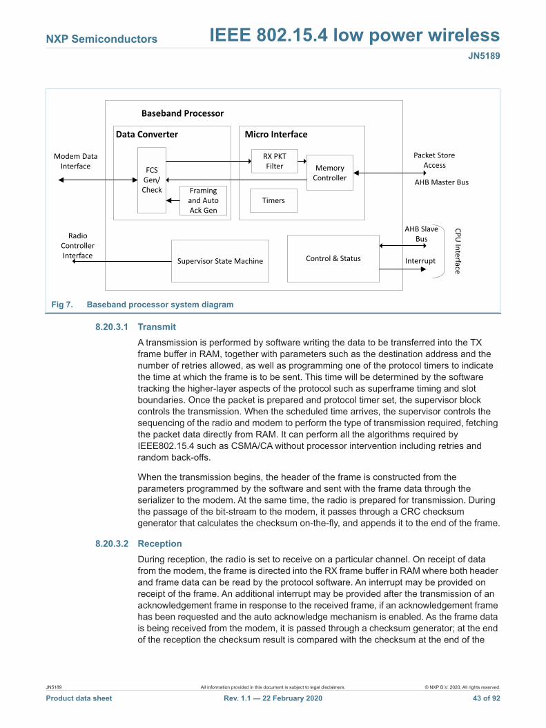
NXP Semiconductors IEEE 802.15.4 low power wirelessJN5189
8.20.3.1 TransmitA transmission is performed by software writing the data to be transferred into the TX frame buffer in RAM, together with parameters such as the destination address and the number of retries allowed, as well as programming one of the protocol timers to indicate the time at which the frame is to be sent. This time will be determined by the software tracking the higher-layer aspects of the protocol such as superframe timing and slot boundaries. Once the packet is prepared and protocol timer set, the supervisor block controls the transmission. When the scheduled time arrives, the supervisor controls the sequencing of the radio and modem to perform the type of transmission required, fetching the packet data directly from RAM. It can perform all the algorithms required by IEEE802.15.4 such as CSMA/CA without processor intervention including retries and random back-offs.
When the transmission begins, the header of the frame is constructed from the parameters programmed by the software and sent with the frame data through the serializer to the modem. At the same time, the radio is prepared for transmission. During the passage of the bit-stream to the modem, it passes through a CRC checksum generator that calculates the checksum on-the-fly, and appends it to the end of the frame.
8.20.3.2 ReceptionDuring reception, the radio is set to receive on a particular channel. On receipt of data from the modem, the frame is directed into the RX frame buffer in RAM where both header and frame data can be read by the protocol software. An interrupt may be provided on receipt of the frame. An additional interrupt may be provided after the transmission of an acknowledgement frame in response to the received frame, if an acknowledgement frame has been requested and the auto acknowledge mechanism is enabled. As the frame data is being received from the modem, it is passed through a checksum generator; at the end of the reception the checksum result is compared with the checksum at the end of the
Fig 7. Baseband processor system diagram
FCS Gen/Check
Micro Interface
Baseband Processor
Packet Store Access
Modem Data Interface
Radio Controller Interface Control & Status
AHB Slave Bus
Supervisor State Machine
Memory Controller
RX PKT Filter
Data Converter
Framing and Auto Ack Gen
Timers
Interrupt
CPU Interface
AHB Master Bus
JN5189 All information provided in this document is subject to legal disclaimers. © NXP B.V. 2020. All rights reserved.
Product data sheet Rev. 1.1 — 22 February 2020 43 of 92
NXP Semiconductors IEEE 802.15.4 low power wirelessJN5189
message to ensure that the data has been received correctly. During reception, the modem determines the Link Quality, which is made available at the end of the reception as part of the requirements of IEEE 802.15.4.
8.20.3.3 Auto acknowledgePart of the protocol allows for transmitted frames to be acknowledged by the destination sending an acknowledge packet within a very short window after the transmitted frame has been received. The baseband processor can automatically construct and send the acknowledgment packet without processor intervention and hence avoid the protocol software being involved in time-critical processing within the acknowledge sequence. The baseband processor can also request an acknowledge for packets being transmitted and handle the reception of acknowledged packets without processor intervention.
8.20.3.4 SecurityThe transmission and reception of secured frames using the Advanced Encryption Standard (AES) algorithm is handled by the stack software. The baseband processor and modem does not perform any encryption or decryption. To transmit an encrypted packet, the data in the packet must be encrypted and written into the RAM and then the baseband processor can be directed to transmit the encrypted data. Similarly, in receive, the encrypted data is written into the RAM by the baseband processor. The stack software must then perform the decryption.
The AES engine provided on chip supports hardware accelerated AES operations and can be used by the stack software or the application.
8.20.4 Antenna diversityAntenna diversity is a technique that maximizes the performance of an antenna system. It allows the radio to switch between two antennas that have very low correlation between their received signals. Typically, this is achieved by spacing two antennae around 0.25 wavelengths apart or by using two orthogonal polarizations. So, if performance is poor, the radio system can switch to the other antenna, with a different probability of success.
In ZigBee operation, using transmit diversity mode, if a packet is transmitted and no acknowledgment is received, the radio system can switch to the other antenna for the retry. Alternatively, antenna diversity can be enabled so that antenna switching will occur in receive mode when waiting for a packet. Receive diversity operates a combined HW timer and SW power threshold mode. In general, the antenna is switched every 60 ms. However, if two preamble symbols are detected, then the antenna switching stops; the software will check whether the signal strength exceeds a threshold. If the signal is too weak, then the antenna selected is switched and the automatic switching will restart. If the signal is strong, the packet reception will continue. The overall system performance depends upon various factors such as the attenuation / isolation between the two antennas, the RF characteristics of the signals received on each antenna.
The JN5189 provides an output (ADO) on DIO7, DIO9 or DIO19 that is asserted on odd numbered retries and optionally its complement (ADE) on DIO6, that can be used to control an antenna switch; this enables antenna diversity to be implemented easily (see the following two figures).
JN5189 All information provided in this document is subject to legal disclaimers. © NXP B.V. 2020. All rights reserved.
Product data sheet Rev. 1.1 — 22 February 2020 44 of 92
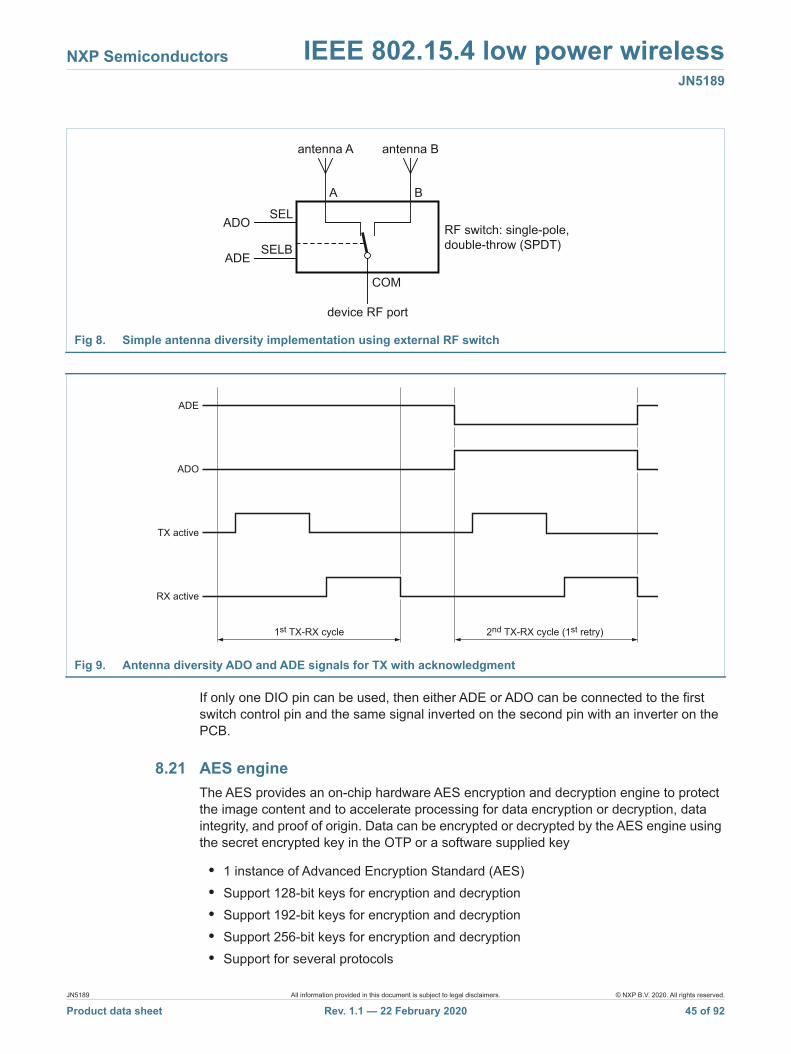
NXP Semiconductors IEEE 802.15.4 low power wirelessJN5189
If only one DIO pin can be used, then either ADE or ADO can be connected to the first switch control pin and the same signal inverted on the second pin with an inverter on the PCB.
8.21 AES engineThe AES provides an on-chip hardware AES encryption and decryption engine to protect the image content and to accelerate processing for data encryption or decryption, data integrity, and proof of origin. Data can be encrypted or decrypted by the AES engine using the secret encrypted key in the OTP or a software supplied key
• 1 instance of Advanced Encryption Standard (AES)• Support 128-bit keys for encryption and decryption• Support 192-bit keys for encryption and decryption• Support 256-bit keys for encryption and decryption• Support for several protocols
Fig 8. Simple antenna diversity implementation using external RF switch
SEL
A
antenna A
device RF port
B
COM
antenna B
SELB
ADO
ADE
RF switch: single-pole,double-throw (SPDT)
Fig 9. Antenna diversity ADO and ADE signals for TX with acknowledgment
ADE
ADO
TX active
RX active
1st TX-RX cycle 2nd TX-RX cycle (1st retry)
JN5189 All information provided in this document is subject to legal disclaimers. © NXP B.V. 2020. All rights reserved.
Product data sheet Rev. 1.1 — 22 February 2020 45 of 92
NXP Semiconductors IEEE 802.15.4 low power wirelessJN5189
– ECB (Electronic Code Book)– CBC (Cipher Block Chaining)– CFB (Cipher Feedback)– OFB (Output Feedback)– CTR (Counter)
• DMA support with DMA triggers for input data and output data
8.22 SPI-bus Flash Interface (SPIFI)The SPI-bus Flash Interface provides support for a master Quad SPI-bus capable of interfacing to a range of SPI devices for high throughput transfer of data between the JN5189 and an external device, such as a memory device.
• 1 Quad SPI-bus Flash Interface (SPIFI) interface to external flash.• Code in the serial flash memory can be executed as if it was in the CPU’s internal
memory space. This is accomplished by mapping the external flash memory directly into the CPU memory space.
Remark: the SPIFI implemented on JN5189 is intended for data access. The cache size is reduced and therefore direct execution from off-chip SPI-bus Flash is not recommended.
• Supports 1-bit, 2-bit, and 4-bit bidirectional serial protocols• Half-duplex protocol compatible with various vendors and devices• Operates at up to 32 MHz• DMA support for transferring data to and from the SPIFI module
8.23 Hash moduleThe Hash function creates a fixed size signature from a block of data. It can be used as part of a scheme to check if data corruption has occurred.
• Supports SHA-1• Supports SHA-2-256• DMA support for efficient operation
8.24 ISO7816 smart card interfaceThe ISO smart card interface block, with suitable external analogue device, can support Smart Card reader applications.
• Compliant with ISO7816 standard• Support of class A (5 V), Class B (3 V) and Class C (1.8 V) contact smart cards• Support of ISO7816 UART interface• Supports the asynchronous protocols (T=0 and T=1) in accordance with ISO7816• Supports synchronous cards
JN5189 All information provided in this document is subject to legal disclaimers. © NXP B.V. 2020. All rights reserved.
Product data sheet Rev. 1.1 — 22 February 2020 46 of 92
NXP Semiconductors IEEE 802.15.4 low power wirelessJN5189
8.25 Random Number GeneratorThe JN5189 integrates a random number generator (RNG) for security purposes. The RNG generates, with suitable software, true non-deterministic random numbers for generating keys, initialization vectors and other random number requirements.
8.26 NTAG I2CSee Table 2 for parts that have NTAG. For devices supporting the internal NTAG device, two device pins are used to connect the JN5189 to the external NFC antenna and matching components. Internally a dedicated I2C interface is used to communicate to the NTAG tag. The NFC tag can be accessed via the NFC antenna even when the device is not powered. One use of the feature is to allow commissioning of a device before it is installed. The field detect line from the NTAG is able to interrupt the processor in active mode and also cause wake-up from all power down modes.
8.26.1 Features
• RF interface NFC forum type 2 tag compliant, operating frequency of 13.56 MHz• Data transfer of 106 kbit/s• Operating distance of up to 100 mm (depending on various parameters, such as field
strength and antenna geometry)• 4 bytes (one page) written including all overhead in 4.8 ms via EEPROM or 0.8 ms via
SRAM (Pass-through mode)• Data integrity of 16-bit CRC, parity, bit coding, bit counting• True anticollision• Unique 7 byte serial number (cascade level 2 according to ISO/IEC 14443-3)• Tag Memory: 1912 bytes freely available with User Read/Write area (478 pages with 4
bytes per pages)• Field programmable RF read-only locking function with static and dynamic lock bits
configurable from both I2C-bus and NFC interfaces• 64 bytes SRAM volatile memory without write endurance limitation• Data retention time of 20 years• Write endurance 200,000 cycles• I2C-bus slave interface supports standard (100 kHz) and Fast (up to 400 kHz) mode• 16 bytes (one block) written in 4.5 ms (EEPROM) or 0.4 ms (SRAM - Pass-through
mode) including all overhead• Configurable field detection pin that can be triggered upon the following events:
– A RF field presence– The first start-of-frame– The selection of the tag only
• 64 byte SRAM buffer for fast transfer of data (Pass-through mode) between the RF and the I2C-bus interfaces located outside the user memory
• Wake up signal at the field detect pin when:– New data has arrived from one interface– Wake up possible from sleep, deep-sleep, power-down and deep power-down
JN5189 All information provided in this document is subject to legal disclaimers. © NXP B.V. 2020. All rights reserved.
Product data sheet Rev. 1.1 — 22 February 2020 47 of 92
NXP Semiconductors IEEE 802.15.4 low power wirelessJN5189
– Data has been read by the receiving interface• Clear arbitration between RF and I2C-bus interfaces:
– First come, first serve strategy– Status flag bits to signal if one interface is busy writing to or reading data from the
EEPROM• Fast read command for faster data reading• Security:
– Manufacturer-programmed 7-byte UID for each device– Capability container with one time programmable bits– Field programmable read-only locking function per page (per 32 pages for the
extended memory section)
8.26.2 General descriptionThe internal NTAG I2C-bus is offering a contactless interface to JN5189T/JN5188T. That passive NFC Forum compliant contactless interface can communicate with JN5189T/JN5188T microcontroller through a dedicated internal I2C-bus interface.
An SRAM mapped into the memory allows a fast data transfer between the NFC antenna and the I2C-bus interface and vice versa, without the write cycle limitations of the EEPROM memory.
The NTAG I2C-bus features a configurable field detection pin, which provides a trigger to the microcontroller depending on the activities at the NFC interface.
Remark: To support the energy harvesting and power the platform through the NFC field, an external NTAGPlus must be populated on the target board.
9. Application design-in information
9.1 JN5189 module reference designsFor customers wishing to integrate the JN5189 device directly into their system, NXPprovides a range of Module Reference Designs.
To ensure the correct performance, it is strongly recommended that where possible the design details provided by the reference designs are used in their exact form for all end designs; this includes component values, pad dimensions, track layouts etc. In order to minimize all risks, it is recommended that the entire layout of the appropriate reference module, if possible, be replicated in the end design.
For full details, see web site or Contact technical support.
9.2 Schematic diagramThe PCB schematic and layout rules detailed in this data sheet must be followed. Failure to do so will likely result in the JN5189 failing to meet the performance specification detailed in this data sheet and the worst case may result in the device not functioning in the end application.
JN5189 All information provided in this document is subject to legal disclaimers. © NXP B.V. 2020. All rights reserved.
Product data sheet Rev. 1.1 — 22 February 2020 48 of 92
NXP Semiconductors IEEE 802.15.4 low power wirelessJN5189
A schematic diagram of the reference module is shown in Figure 10. Details of component values and PCB layout constraints can be found in Table 10.
The paddle should be connected directly to ground. Any pads that require connection to ground should do so by connecting directly to the paddle.
The JN5189 will enter UART programming mode if IN System Programming Entry (PIO5) pin 8 is low during RESET release.
The preferred communication interface is USART0 pins (PIO8/USART0_TXD pin11 and PIO9/USART0_RXD pin12).
For single-ended antennas or connectors, a balun is not required. However, an external filtering is needed. In receiver, the RFIO pin shows a 50 impedance and external filtering (R5, C25, L2, C24) is needed in transmission to filter efficiently harmonics. These components are critical and must be placed close to the JN5189 pins and analog ground.
The reference PCB is designed to present an accurate match to a 50 resistive network as well as provide a DC path to the final output stage or antenna. Users wishing to match to other active devices such as amplifiers must design their networks to match to 50 at the output of the JN5189.
The paddle must be connected directly to the ground. Any pads that require connection to the ground should do so by connecting directly to the paddle.
Fig 10. Application diagram – battery powered solution
aaa-021971
C13 100 nF
C14
C19
C12C11
2.4 GHzantenna
C10 100 nF
VBAT VBAT (Pin 28) VDDE (Pin 20)
RF_IO (Pin 37)
LX (Pin 29)
VDD_RADIO (Pin 35)
FB (Pin 31)
10 μF
L4
DC/DCCONVERTER
PMU/CPU/
RADIOTRANSCEIVER
32 MHzOSCILLATOR
XTAL_N (Pin 2)
XTAL_P (Pin 1)
XTAL_32k_NX(Pin 34)
XTAL_32k_P
I/O
32 kHzOSCILLATOR
C25 R5
3.3 nH
C24
VDD_PMU (Pin 32)
(Pin 33)
Y1X2
NFC antenna
LA (Pin 40)
LB (Pin 39)
C20C21
JN5189T
47 pFC1
4.7 μH
10 μF
47 pF
NC NC
L2
0 Ω2 pF 1.2 pF
100 nF
1.9 to 3.6 V
MEMORY
JN5189 All information provided in this document is subject to legal disclaimers. © NXP B.V. 2020. All rights reserved.
Product data sheet Rev. 1.1 — 22 February 2020 49 of 92
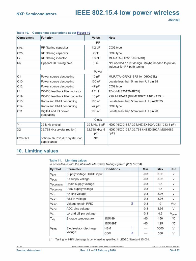
NXP Semiconductors IEEE 802.15.4 low power wirelessJN5189
10. Limiting values
[1] Testing for HBM discharge is performed as specified in JEDEC Standard JS-001.
Table 10. Component descriptions about Figure 10Component Function Value Note
RF
C24 RF filtering capacitor 1.2 pF COG type
C25 RF filtering capacitor 2 pF COG typeL2 RF filtering inductor 3.3 nH MURATA (LQW15AN3N3B)R5 Optional RF tuning area 0 Not needed on ref design. Maybe needed to put an
inductor for RF path tuning Power
C1 Power source decoupling 10 μF MURATA (GRM21BR71A106KA73L)C10 Power source decoupling 100 nF Locate less than 5mm from U1 pin 28C12 Power source decoupling 47 pF COG typeL4 DC-DC feedback filter inductor 4.7 μH TDK (MLZ2012M4R7H)C19 DC-DC feedback filter capacitor 10 μF X7R MURATA (GRM21BR71A106KA73L)C13 Radio and PMU decoupling 100 nF Locate less than 5mm from U1 pins32/35C14 Radio and PMU decoupling 47 pF COG typeC11 DigitL4 and IO power
decoupling 100 nF Locate less than 5mm from U1 pin 20
ClockY1 32 MHz crystal 32 MHz, 6 pF NDK (NX2016SA 32 MHZ EXS00A-CS11213 6 pF)X2 32.768 kHz crystal (option) 32.768 kHz, 6
pFNDK (NX2012SA 32.768 kHZ EXS00A-MU01089 6pF)
C20-C21 optional 32.768 kHz crystal load capacitance
NC
Table 11. Limiting values In accordance with the Absolute Maximum Rating System (IEC 60134).
Symbol Parameter Conditions Min Max UnitVBAT Supply voltage DCDC input -0.3 3.96 VVDDE IO supply voltage -0.3 3.96 VVDD(Radio) Radio supply voltage -0.3 1.6 VVDD(PMU) PMU supply voltage -0.3 1.6 VVIO IO pins voltage -0.3 3.96 VVRST RSTIN voltage -0.3 3.96 VVRFIO Voltage on pin RFIO [3] -0.3 0 VDC
VADC ADC pins voltage -0.3 3.96 VVLx LA and LB pin voltage -0.3 4.6 Vpeak
Tstg Storage temperature JN5189 -40 150 CJN5189T -40 125 C
VESD Electrostatic discharge voltage
HBM [1] 3000 VCDM [2] 500 V
JN5189 All information provided in this document is subject to legal disclaimers. © NXP B.V. 2020. All rights reserved.
Product data sheet Rev. 1.1 — 22 February 2020 50 of 92
NXP Semiconductors IEEE 802.15.4 low power wirelessJN5189
[2] Testing for CDM discharge is performed as specified in JEDEC Standard JESD22-C101.
[3] Primary input of RF transformer connected to the ground. No DC voltage.
11. Recommended operating conditions
12. Thermal characteristics
Table 12. Operating conditions Symbol Parameter Conditions Min Max UnitVBAT DCDC supply voltage 1.9 3.6 VVDDE IO supply voltage 1.9 3.6 VTJ JN5189 temperature -40 125 CTJ JN5189T temperature TAG not activated
for Temp > 105 C-40 125 C
TAG activated -40 105 C
Table 13. Thermal characteristics Symbol Parameter Conditions Min Typ Max UnitRth(j-a) Thermal resistance from junction
to ambient 28 K/W
Rth(j-c) Thermal resistance from junction to case
4 K/W
Tj(max) JN5189 maximum junction temperature
125 C
Tj(max) JN5189T maximum junction temperature
TAG not activated for Temp > 105 C
125 C
TAG activated 105 C
JN5189 All information provided in this document is subject to legal disclaimers. © NXP B.V. 2020. All rights reserved.
Product data sheet Rev. 1.1 — 22 February 2020 51 of 92
NXP Semiconductors IEEE 802.15.4 low power wirelessJN5189
13. Static characteristics
13.1 Power consumption in Low-power mode
[1] Values achieved when application uses the optimized voltage configuration for power down. Any additional 4 KB RAM increases leakage current in typical condition by 105 nA.
[2] Will be added to the power down current consumption if used.
[3] Need to have retention on RAMBank7 (4 KB).
13.2 Power consumption in Active mode
Table 14. Typical current consumption in Low-power mode characteristics VBAT = 1.9 V to 3.6 V, Tamb = 25 °C
Symbol Parameter Conditions Min Typ Max UnitIDD supply
currentDeep power-down (everything is powered off, wake-up on HW reset only)
250 nA
Deep power-down-IO (everything is poweredoff, wake-up on HW reset only or an event onany of the 22 GPIOs and NTAG interrupt)
350 nA
Power-down (wake-up on HW reset or an IO event, wake-up timer ON, 32 kHz FRO on, no SRAM retention)
800 nA
Power-down-4K (wake-up on HW reset or an IO event, wake-up timer on, 32 kHz FRO on, with 4 KB SRAM retention])
[1] 1025 nA
Power-down-8K (wake-up on HW reset or an IO event, wake-up timer on, 32 kHz FRO on, with 8 KB SRAM retention)
[1] 1120 nA
Power down - RTC 1 kHz [2] 200 nAPower down - RTC 1 Hz [2] 200 nAPower down - per wake-up timer0 or timer1 / 32 kHz FRO 200 nAPower down - per wake-up timer0 or timer1 / 32 kHz XTAL 200 nAPower down - BOD VBAT [2] 300 nAPower down - wake up on COM interfaces [2] [3] 440 nA
Table 15. Typical current consumption in Active mode characteristics VBAT = 1.9 V to 3.6 V, Tamb = 25 °C.
Symbol Parameter Conditions Min Typ Max UnitIDD supply current radio in RX mode (IEEE 802.15.4) 4.3 mA
radio in TX mode (IEEE 802.15.4)output power 0 dBm 7.36 mAoutput power +3 dBm 9.44 mAoutput power +10 dBm 20.28 mA
JN5189 All information provided in this document is subject to legal disclaimers. © NXP B.V. 2020. All rights reserved.
Product data sheet Rev. 1.1 — 22 February 2020 52 of 92
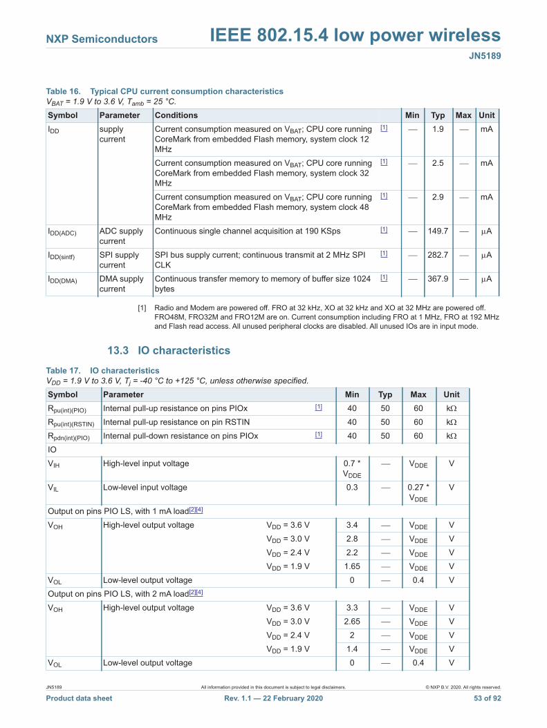
NXP Semiconductors IEEE 802.15.4 low power wirelessJN5189
[1] Radio and Modem are powered off. FRO at 32 kHz, XO at 32 kHz and XO at 32 MHz are powered off. FRO48M, FRO32M and FRO12M are on. Current consumption including FRO at 1 MHz, FRO at 192 MHz and Flash read access. All unused peripheral clocks are disabled. All unused IOs are in input mode.
13.3 IO characteristics
Table 16. Typical CPU current consumption characteristics VBAT = 1.9 V to 3.6 V, Tamb = 25 °C.
Symbol Parameter Conditions Min Typ Max UnitIDD supply
currentCurrent consumption measured on VBAT; CPU core running CoreMark from embedded Flash memory, system clock 12 MHz
[1] 1.9 mA
Current consumption measured on VBAT; CPU core running CoreMark from embedded Flash memory, system clock 32 MHz
[1] 2.5 mA
Current consumption measured on VBAT; CPU core running CoreMark from embedded Flash memory, system clock 48 MHz
[1] 2.9 mA
IDD(ADC) ADC supply current
Continuous single channel acquisition at 190 KSps [1] 149.7 A
IDD(sintf) SPI supply current
SPI bus supply current; continuous transmit at 2 MHz SPI CLK
[1] 282.7 A
IDD(DMA) DMA supply current
Continuous transfer memory to memory of buffer size 1024 bytes
[1] 367.9 A
Table 17. IO characteristics VDD = 1.9 V to 3.6 V, Tj = -40 °C to +125 °C, unless otherwise specified.
Symbol Parameter Min Typ Max UnitRpu(int)(PIO) Internal pull-up resistance on pins PIOx [1] 40 50 60 kRpu(int)(RSTIN) Internal pull-up resistance on pin RSTIN 40 50 60 kRpdn(int)(PIO) Internal pull-down resistance on pins PIOx [1] 40 50 60 kIOVIH High-level input voltage 0.7 *
VDDE
VDDE V
VIL Low-level input voltage 0.3 0.27 * VDDE
V
Output on pins PIO LS, with 1 mA load[2][4]
VOH High-level output voltage VDD = 3.6 V 3.4 VDDE VVDD = 3.0 V 2.8 VDDE VVDD = 2.4 V 2.2 VDDE VVDD = 1.9 V 1.65 VDDE V
VOL Low-level output voltage 0 0.4 VOutput on pins PIO LS, with 2 mA load[2][4]
VOH High-level output voltage VDD = 3.6 V 3.3 VDDE VVDD = 3.0 V 2.65 VDDE VVDD = 2.4 V 2 VDDE VVDD = 1.9 V 1.4 VDDE V
VOL Low-level output voltage 0 0.4 V
JN5189 All information provided in this document is subject to legal disclaimers. © NXP B.V. 2020. All rights reserved.
Product data sheet Rev. 1.1 — 22 February 2020 53 of 92
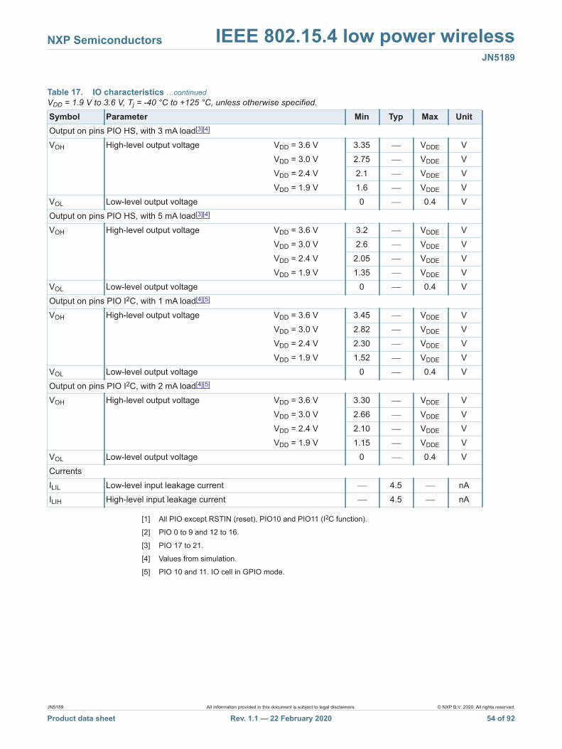
NXP Semiconductors IEEE 802.15.4 low power wirelessJN5189
[1] All PIO except RSTIN (reset), PIO10 and PIO11 (I2C function).
[2] PIO 0 to 9 and 12 to 16.
[3] PIO 17 to 21.
[4] Values from simulation.
[5] PIO 10 and 11. IO cell in GPIO mode.
Output on pins PIO HS, with 3 mA load[3][4]
VOH High-level output voltage VDD = 3.6 V 3.35 VDDE VVDD = 3.0 V 2.75 VDDE VVDD = 2.4 V 2.1 VDDE VVDD = 1.9 V 1.6 VDDE V
VOL Low-level output voltage 0 0.4 VOutput on pins PIO HS, with 5 mA load[3][4]
VOH High-level output voltage VDD = 3.6 V 3.2 VDDE VVDD = 3.0 V 2.6 VDDE VVDD = 2.4 V 2.05 VDDE VVDD = 1.9 V 1.35 VDDE V
VOL Low-level output voltage 0 0.4 VOutput on pins PIO I2C, with 1 mA load[4][5]
VOH High-level output voltage VDD = 3.6 V 3.45 VDDE VVDD = 3.0 V 2.82 VDDE VVDD = 2.4 V 2.30 VDDE VVDD = 1.9 V 1.52 VDDE V
VOL Low-level output voltage 0 0.4 VOutput on pins PIO I2C, with 2 mA load[4][5]
VOH High-level output voltage VDD = 3.6 V 3.30 VDDE VVDD = 3.0 V 2.66 VDDE VVDD = 2.4 V 2.10 VDDE VVDD = 1.9 V 1.15 VDDE V
VOL Low-level output voltage 0 0.4 VCurrentsILIL Low-level input leakage current 4.5 nAILIH High-level input leakage current 4.5 nA
Table 17. IO characteristics …continuedVDD = 1.9 V to 3.6 V, Tj = -40 °C to +125 °C, unless otherwise specified.
Symbol Parameter Min Typ Max Unit
JN5189 All information provided in this document is subject to legal disclaimers. © NXP B.V. 2020. All rights reserved.
Product data sheet Rev. 1.1 — 22 February 2020 54 of 92
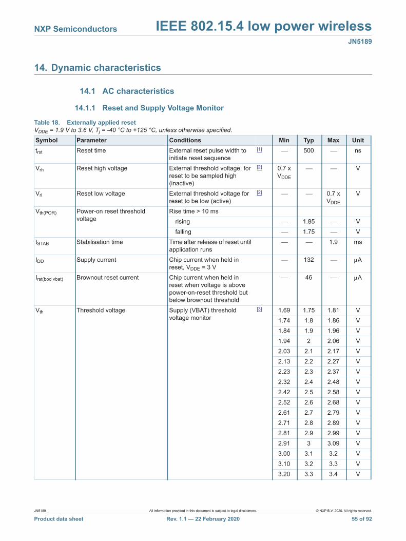
NXP Semiconductors IEEE 802.15.4 low power wirelessJN5189
14. Dynamic characteristics
14.1 AC characteristics
14.1.1 Reset and Supply Voltage Monitor
Table 18. Externally applied reset VDDE = 1.9 V to 3.6 V, Tj = -40 °C to +125 °C, unless otherwise specified.
Symbol Parameter Conditions Min Typ Max Unittrst Reset time External reset pulse width to
initiate reset sequence[1] 500 ns
Vrh Reset high voltage External threshold voltage, for reset to be sampled high (inactive)
[2] 0.7 x VDDE
V
Vrl Reset low voltage External threshold voltage for reset to be low (active)
[2] 0.7 x VDDE
V
Vth(POR) Power-on reset threshold voltage
Rise time > 10 msrising 1.85 Vfalling 1.75 V
tSTAB Stabilisation time Time after release of reset until application runs
1.9 ms
IDD Supply current Chip current when held in reset, VDDE = 3 V
132 A
Irst(bod vbat) Brownout reset current Chip current when held in reset when voltage is above power-on-reset threshold but below brownout threshold
46 A
Vth Threshold voltage Supply (VBAT) threshold voltage monitor
[3] 1.69 1.75 1.81 V1.74 1.8 1.86 V1.84 1.9 1.96 V1.94 2 2.06 V2.03 2.1 2.17 V2.13 2.2 2.27 V2.23 2.3 2.37 V2.32 2.4 2.48 V2.42 2.5 2.58 V2.52 2.6 2.68 V2.61 2.7 2.79 V2.71 2.8 2.89 V2.81 2.9 2.99 V2.91 3 3.09 V3.00 3.1 3.2 V3.10 3.2 3.3 V3.20 3.3 3.4 V
JN5189 All information provided in this document is subject to legal disclaimers. © NXP B.V. 2020. All rights reserved.
Product data sheet Rev. 1.1 — 22 February 2020 55 of 92
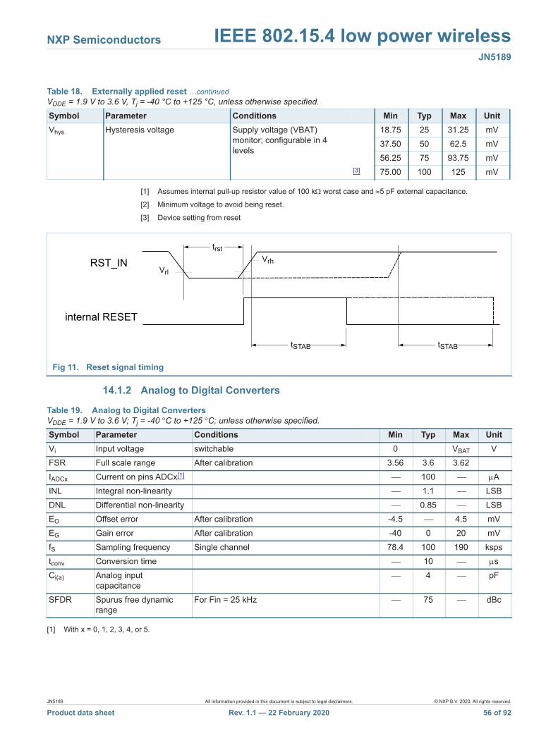
NXP Semiconductors IEEE 802.15.4 low power wirelessJN5189
[1] Assumes internal pull-up resistor value of 100 k worst case and 5 pF external capacitance.
[2] Minimum voltage to avoid being reset.
[3] Device setting from reset
14.1.2 Analog to Digital Converters
[1] With x = 0, 1, 2, 3, 4, or 5.
Vhys Hysteresis voltage Supply voltage (VBAT) monitor; configurable in 4 levels
18.75 25 31.25 mV37.50 50 62.5 mV56.25 75 93.75 mV
[3] 75.00 100 125 mV
Table 18. Externally applied reset …continuedVDDE = 1.9 V to 3.6 V, Tj = -40 °C to +125 °C, unless otherwise specified.
Symbol Parameter Conditions Min Typ Max Unit
Fig 11. Reset signal timing
tSTAB
Vrh
trst
Vrl
internal RESET
RST_IN
tSTAB
Table 19. Analog to Digital Converters VDDE = 1.9 V to 3.6 V; Tj = -40 °C to +125 °C; unless otherwise specified.
Symbol Parameter Conditions Min Typ Max UnitVi Input voltage switchable 0 VBAT VFSR Full scale range After calibration 3.56 3.6 3.62IADCx Current on pins ADCx[1] 100 AINL Integral non-linearity 1.1 LSBDNL Differential non-linearity 0.85 LSBEO Offset error After calibration -4.5 4.5 mVEG Gain error After calibration -40 0 20 mVfS Sampling frequency Single channel 78.4 100 190 kspstconv Conversion time 10 sCi(a) Analog input
capacitance 4 pF
SFDR Spurus free dynamic range
For Fin = 25 kHz 75 dBc
JN5189 All information provided in this document is subject to legal disclaimers. © NXP B.V. 2020. All rights reserved.
Product data sheet Rev. 1.1 — 22 February 2020 56 of 92
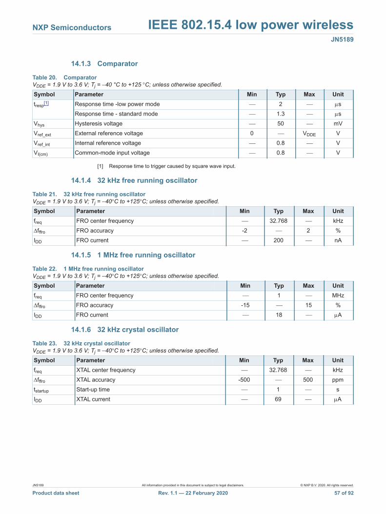
NXP Semiconductors IEEE 802.15.4 low power wirelessJN5189
14.1.3 Comparator
[1] Response time to trigger caused by square wave input.
14.1.4 32 kHz free running oscillator
14.1.5 1 MHz free running oscillator
14.1.6 32 kHz crystal oscillator
Table 20. Comparator VDDE = 1.9 V to 3.6 V; Tj = −40 °C to +125 °C; unless otherwise specified.
Symbol Parameter Min Typ Max Unittresp[1] Response time -low power mode 2 s
Response time - standard mode 1.3 sVhys Hysteresis voltage 50 mVVref_ext External reference voltage 0 VDDE VVref_int Internal reference voltage 0.8 VVI(cm) Common-mode input voltage 0.8 V
Table 21. 32 kHz free running oscillator VDDE = 1.9 V to 3.6 V; Tj = −40°C to +125°C; unless otherwise specified.
Symbol Parameter Min Typ Max Unitfreq FRO center frequency 32.768 kHzfffro FRO accuracy -2 2 %IDD FRO current 200 nA
Table 22. 1 MHz free running oscillator VDDE = 1.9 V to 3.6 V; Tj = −40°C to +125°C; unless otherwise specified.
Symbol Parameter Min Typ Max Unitfreq FRO center frequency 1 MHzfffro FRO accuracy -15 15 %IDD FRO current 18 A
Table 23. 32 kHz crystal oscillator VDDE = 1.9 V to 3.6 V; Tj = −40°C to +125°C; unless otherwise specified.
Symbol Parameter Min Typ Max Unitfreq XTAL center frequency 32.768 kHzfffro XTAL accuracy -500 500 ppmtstartup Start-up time 1 sIDD XTAL current 69 A
JN5189 All information provided in this document is subject to legal disclaimers. © NXP B.V. 2020. All rights reserved.
Product data sheet Rev. 1.1 — 22 February 2020 57 of 92
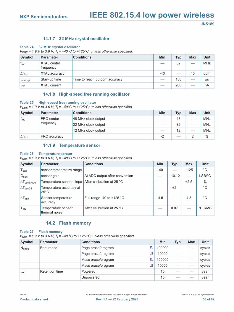
NXP Semiconductors IEEE 802.15.4 low power wirelessJN5189
14.1.7 32 MHz crystal oscillator
14.1.8 High-speed free running oscillator
14.1.9 Temperature sensor
14.2 Flash memory
Table 24. 32 MHz crystal oscillator VDDE = 1.9 V to 3.6 V; Tj = −40°C to +125°C; unless otherwise specified.
Symbol Parameter Conditions Min Typ Max Unitfreq XTAL center
frequency 32 MHz
fffro XTAL accuracy -40 40 ppmtstartup Start-up time Time to reach 50 ppm accuracy 150 sIDD XTAL current 200 nA
Table 25. High-speed free running oscillator VDDE = 1.9 V to 3.6 V; Tj = −40°C to +125°C; unless otherwise specified.
Symbol Parameter Conditions Min Typ Max Unitfreq FRO center
frequency48 MHz clock output 48 MHz32 MHz clock output 32 MHz12 MHz clock output 12 MHz
fffro FRO accuracy -2 2 %
Table 26. Temperature sensor VDDE = 1.9 V to 3.6 V; Tj = −40°C to +125°C; unless otherwise specified.
Symbol Parameter Conditions Min Typ Max UnitTsen sensor temperature range 40 +125 °CGsen sensor gain At ADC output after conversion 10.12 LSB/°CTsenSlope Temperature sensor slope After calibration at 25 °C 2.5 %Tsen25 Temperature accuracy at
25°C 2 °C
Tsen Sensor temperature accuracy
Full range -40 to +125 °C -4.5 4.5 °C
TTN Temperature sensor thermal noise
After calibration at 25 °C 0.07 °C·RMS
Table 27. Flash memoryVDDE = 1.9 V to 3.6 V; Tj = −40 °C to +125 °C; unless otherwise specified.
Symbol Parameter Conditions Min Typ Max UnitNendu Endurance Page erase/program [1] 100000 cycles
Page erase/program [2] 10000 cyclesMass erase/program [1] 100000 cyclesMass erase/program [2] 10000 cycles
tret Retention time Powered 10 yearUnpowered 10 year
JN5189 All information provided in this document is subject to legal disclaimers. © NXP B.V. 2020. All rights reserved.
Product data sheet Rev. 1.1 — 22 February 2020 58 of 92
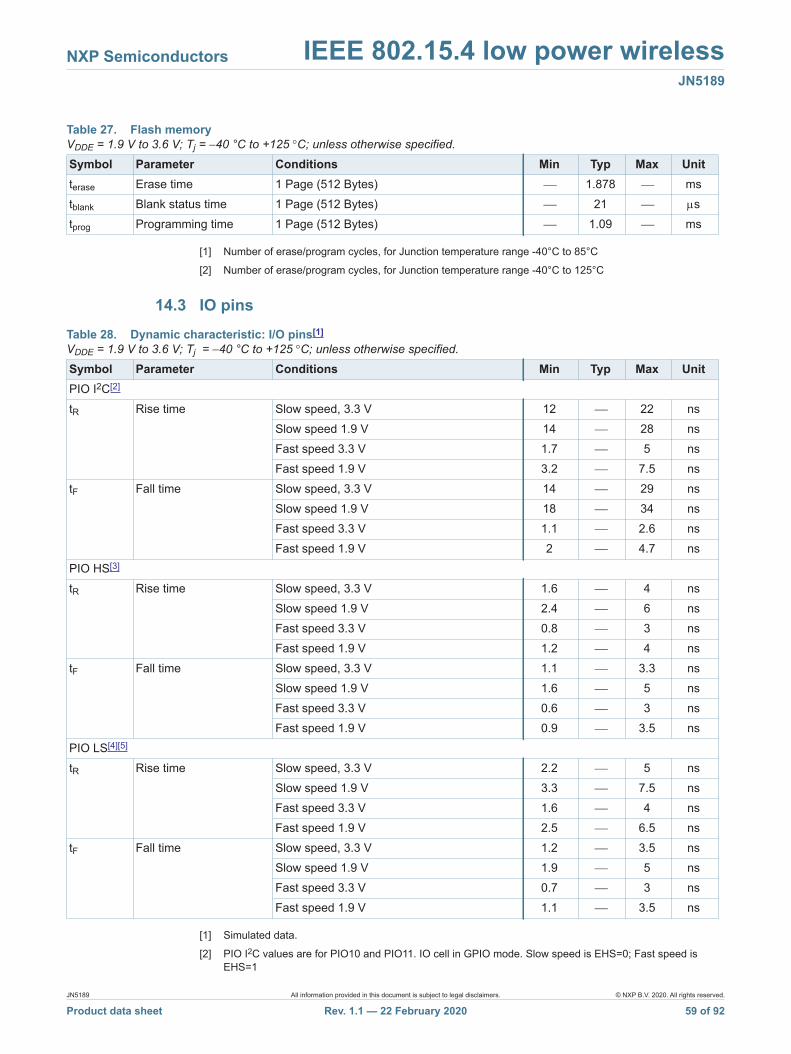
NXP Semiconductors IEEE 802.15.4 low power wirelessJN5189
[1] Number of erase/program cycles, for Junction temperature range -40°C to 85°C
[2] Number of erase/program cycles, for Junction temperature range -40°C to 125°C
14.3 IO pins
[1] Simulated data.
[2] PIO I2C values are for PIO10 and PIO11. IO cell in GPIO mode. Slow speed is EHS=0; Fast speed is EHS=1
terase Erase time 1 Page (512 Bytes) 1.878 mstblank Blank status time 1 Page (512 Bytes) 21 stprog Programming time 1 Page (512 Bytes) 1.09 ms
Table 27. Flash memoryVDDE = 1.9 V to 3.6 V; Tj = −40 °C to +125 °C; unless otherwise specified.
Symbol Parameter Conditions Min Typ Max Unit
Table 28. Dynamic characteristic: I/O pins[1]
VDDE = 1.9 V to 3.6 V; Tj = −40 °C to +125 °C; unless otherwise specified.
Symbol Parameter Conditions Min Typ Max UnitPIO I2C[2] tR Rise time Slow speed, 3.3 V 12 22 ns
Slow speed 1.9 V 14 28 nsFast speed 3.3 V 1.7 5 nsFast speed 1.9 V 3.2 7.5 ns
tF Fall time Slow speed, 3.3 V 14 29 nsSlow speed 1.9 V 18 34 nsFast speed 3.3 V 1.1 2.6 nsFast speed 1.9 V 2 4.7 ns
PIO HS[3]
tR Rise time Slow speed, 3.3 V 1.6 4 nsSlow speed 1.9 V 2.4 6 nsFast speed 3.3 V 0.8 3 nsFast speed 1.9 V 1.2 4 ns
tF Fall time Slow speed, 3.3 V 1.1 3.3 nsSlow speed 1.9 V 1.6 5 nsFast speed 3.3 V 0.6 3 nsFast speed 1.9 V 0.9 3.5 ns
PIO LS[4][5]
tR Rise time Slow speed, 3.3 V 2.2 5 nsSlow speed 1.9 V 3.3 7.5 nsFast speed 3.3 V 1.6 4 nsFast speed 1.9 V 2.5 6.5 ns
tF Fall time Slow speed, 3.3 V 1.2 3.5 nsSlow speed 1.9 V 1.9 5 nsFast speed 3.3 V 0.7 3 nsFast speed 1.9 V 1.1 3.5 ns
JN5189 All information provided in this document is subject to legal disclaimers. © NXP B.V. 2020. All rights reserved.
Product data sheet Rev. 1.1 — 22 February 2020 59 of 92
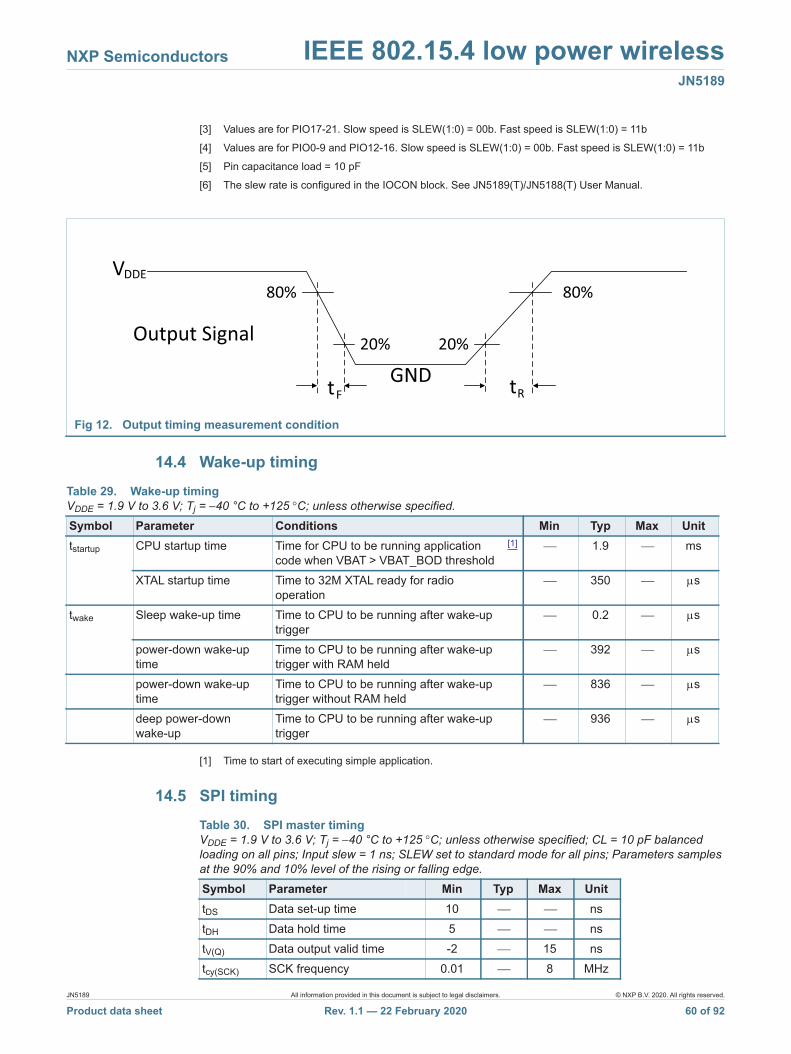
NXP Semiconductors IEEE 802.15.4 low power wirelessJN5189
[3] Values are for PIO17-21. Slow speed is SLEW(1:0) = 00b. Fast speed is SLEW(1:0) = 11b
[4] Values are for PIO0-9 and PIO12-16. Slow speed is SLEW(1:0) = 00b. Fast speed is SLEW(1:0) = 11b
[5] Pin capacitance load = 10 pF
[6] The slew rate is configured in the IOCON block. See JN5189(T)/JN5188(T) User Manual.
14.4 Wake-up timing
[1] Time to start of executing simple application.
14.5 SPI timing
Fig 12. Output timing measurement condition
t t
80% 80%
20% 20%
V
GND
Output Signal
F R
DDE
Table 29. Wake-up timingVDDE = 1.9 V to 3.6 V; Tj = −40 °C to +125 °C; unless otherwise specified.
Symbol Parameter Conditions Min Typ Max Unittstartup CPU startup time Time for CPU to be running application
code when VBAT > VBAT_BOD threshold [1] 1.9 ms
XTAL startup time Time to 32M XTAL ready for radio operation
350 s
twake Sleep wake-up time Time to CPU to be running after wake-up trigger
0.2 s
power-down wake-up time
Time to CPU to be running after wake-up trigger with RAM held
392 s
power-down wake-up time
Time to CPU to be running after wake-up trigger without RAM held
836 s
deep power-down wake-up
Time to CPU to be running after wake-up trigger
936 s
Table 30. SPI master timingVDDE = 1.9 V to 3.6 V; Tj = −40 °C to +125 °C; unless otherwise specified; CL = 10 pF balanced loading on all pins; Input slew = 1 ns; SLEW set to standard mode for all pins; Parameters samples at the 90% and 10% level of the rising or falling edge.
Symbol Parameter Min Typ Max UnittDS Data set-up time 10 nstDH Data hold time 5 nstV(Q) Data output valid time -2 15 nstcy(SCK) SCK frequency 0.01 8 MHz
JN5189 All information provided in this document is subject to legal disclaimers. © NXP B.V. 2020. All rights reserved.
Product data sheet Rev. 1.1 — 22 February 2020 60 of 92

NXP Semiconductors IEEE 802.15.4 low power wirelessJN5189
[1] Pre-delay can be configured to increase this time in steps of 1 SCK cycle
[2] Post-delay can be configured to increase this time in steps of 1 SCK cycle
[1] Pre-delay can be configured to increase this time in steps of 1 SCK cycle
[2] Post-delay can be configured to increase this time in steps of 1 SCK cycle
Duty cycle 45 50 55 %tSS SSEL low before SCK
edge[1] 1 SCK
cyclestSH SSEL low after last SCK
edge[2] 0.5 SCK
cycles
Table 31. SPI slave timingVDDE = 1.9 V to 3.6 V; Tj = −40 °C to +125 °C; unless otherwise specified; CL = 10 pF balanced loading on all pins; Input slew = 1 ns; SLEW set to standard mode for all pins; Parameters samples at the 90% and 10% level of the rising or falling edge.
Symbol Parameter Min Typ Max UnittDS Data set-up time 12 nstDH Data hold time 5 nstV(Q) Data output valid time 0 35 nstcy(SCK) SCK frequency 8 MHztSS SSEL low before SCK edge [1] 1 nstSH SSEL low after last SCK edge [2] 0.5 ns
Table 30. SPI master timingVDDE = 1.9 V to 3.6 V; Tj = −40 °C to +125 °C; unless otherwise specified; CL = 10 pF balanced loading on all pins; Input slew = 1 ns; SLEW set to standard mode for all pins; Parameters samples at the 90% and 10% level of the rising or falling edge.
Symbol Parameter Min Typ Max Unit
JN5189 All information provided in this document is subject to legal disclaimers. © NXP B.V. 2020. All rights reserved.
Product data sheet Rev. 1.1 — 22 February 2020 61 of 92
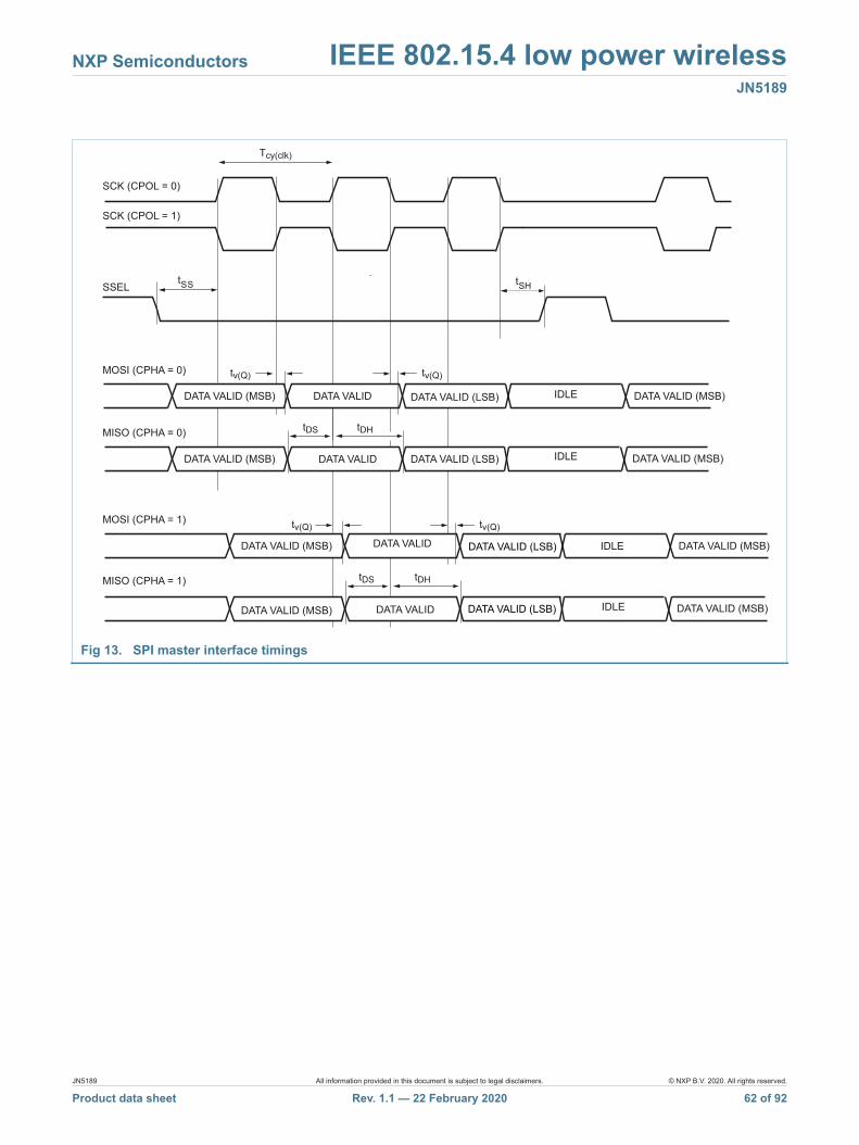
NXP Semiconductors IEEE 802.15.4 low power wirelessJN5189
Fig 13. SPI master interface timings
SCK (CPOL = 0)
MOSI (CPHA = 1)
SSEL
MISO (CPHA = 1)
Tcy(clk)
tDS tDH
tv(Q)
DATA VALID
tv(Q)
SCK (CPOL = 1)
DATA VALID
MOSI (CPHA = 0)
MISO (CPHA = 0) tDS tDH
DATA VALID (MSB) DATA VALID (MSB)DATA VALID
DATA VALID (LSB)
DATA VALID (LSB)
tv(Q)
DATA VALID (MSB) DATA VALID
tv(Q)
DATA VALID (MSB)
DATA VALID (MSB)
DATA VALID (MSB)
IDLE
IDLE
IDLE
IDLE
SSt SHt
DATA VALID (MSB)
DATA VALID (MSB)
DATA VALID (LSB)
DATA VALID (LSB)
JN5189 All information provided in this document is subject to legal disclaimers. © NXP B.V. 2020. All rights reserved.
Product data sheet Rev. 1.1 — 22 February 2020 62 of 92
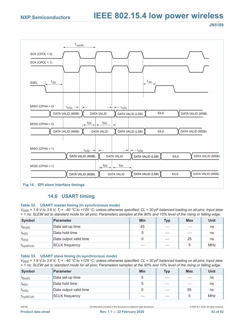
NXP Semiconductors IEEE 802.15.4 low power wirelessJN5189
14.6 USART timing
Fig 14. SPI slave interface timings
SCK (CPOL = 0)
MISO (CPHA = 1)
SSEL
MOSI (CPHA = 1)
Tcy(clk)
tDS tDH
tv(Q)
DATA VALID
tv(Q)
SCK (CPOL = 1)
DATA VALID
MISO (CPHA = 0)
MOSI (CPHA = 0) tDS tDH
DATA VALID (MSB) DATA VALID (MSB)DATA VALID
DATA VALID (LSB)
DATA VALID (LSB)
tv(Q)
DATA VALID (MSB) DATA VALID
tv(Q)
DATA VALID (MSB)
DATA VALID (MSB)
DATA VALID (MSB)IDLE
IDLE
IDLE
IDLE
SSt SHt
DATA VALID (MSB)
DATA VALID (MSB)
DATA VALID (LSB)
DATA VALID (LSB)
Table 32. USART master timing (in synchronous mode)VDDE = 1.9 V to 3.6 V; Tj = −40 °C to +125 °C; unless otherwise specified; CL = 30 pF balanced loading on all pins; Input slew = 1 ns; SLEW set to standard mode for all pins; Parameters samples at the 90% and 10% level of the rising or falling edge.
Symbol Parameter Min Typ Max UnittSU(D) Data set-up time 45 nsth(D) Data hold time 5 nstV(Q) Data output valid time 0 25 nstcy(SCLK) SCLK frequency 5 MHz
Table 33. USART slave timing (in synchronous mode)VDDE = 1.9 V to 3.6 V; Tj = −40 °C to +125 °C; unless otherwise specified; CL = 30 pF balanced loading on all pins; Input slew = 1 ns; SLEW set to standard mode for all pins; Parameters samples at the 90% and 10% level of the rising or falling edge.
Symbol Parameter Min Typ Max UnittSU(D) Data set-up time 5 nsth(D) Data hold time 5 nstV(Q) Data output valid time 0 55 nstcy(SCLK) SCLK frequency 5 MHz
JN5189 All information provided in this document is subject to legal disclaimers. © NXP B.V. 2020. All rights reserved.
Product data sheet Rev. 1.1 — 22 February 2020 63 of 92
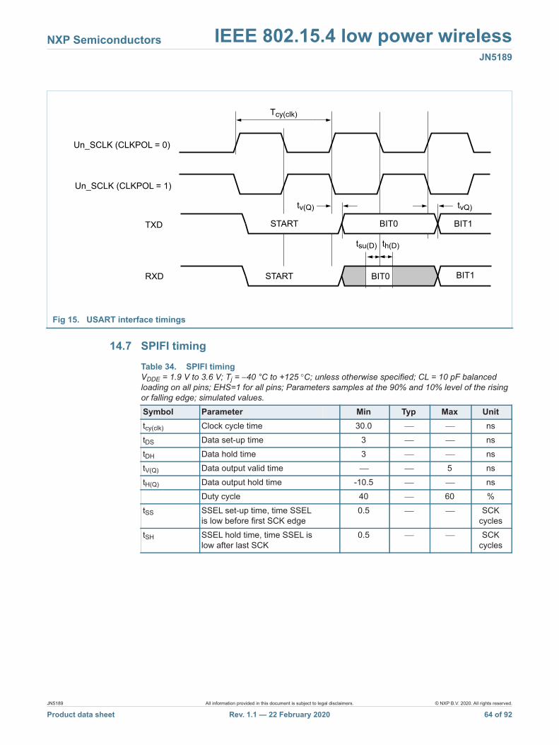
NXP Semiconductors IEEE 802.15.4 low power wirelessJN5189
14.7 SPIFI timing
Fig 15. USART interface timings
Un_SCLK (CLKPOL = 0)
TXD
RXD
Tcy(clk)
tsu(D) th(D)
tv(Q)
START BIT0
tvQ)
Un_SCLK (CLKPOL = 1)
START BIT0 BIT1
BIT1
Table 34. SPIFI timingVDDE = 1.9 V to 3.6 V; Tj = −40 °C to +125 °C; unless otherwise specified; CL = 10 pF balanced loading on all pins; EHS=1 for all pins; Parameters samples at the 90% and 10% level of the rising or falling edge; simulated values.
Symbol Parameter Min Typ Max Unittcy(clk) Clock cycle time 30.0 nstDS Data set-up time 3 nstDH Data hold time 3 nstV(Q) Data output valid time 5 nstH(Q) Data output hold time -10.5 ns
Duty cycle 40 60 %tSS SSEL set-up time, time SSEL
is low before first SCK edge0.5 SCK
cyclestSH SSEL hold time, time SSEL is
low after last SCK0.5 SCK
cycles
JN5189 All information provided in this document is subject to legal disclaimers. © NXP B.V. 2020. All rights reserved.
Product data sheet Rev. 1.1 — 22 February 2020 64 of 92
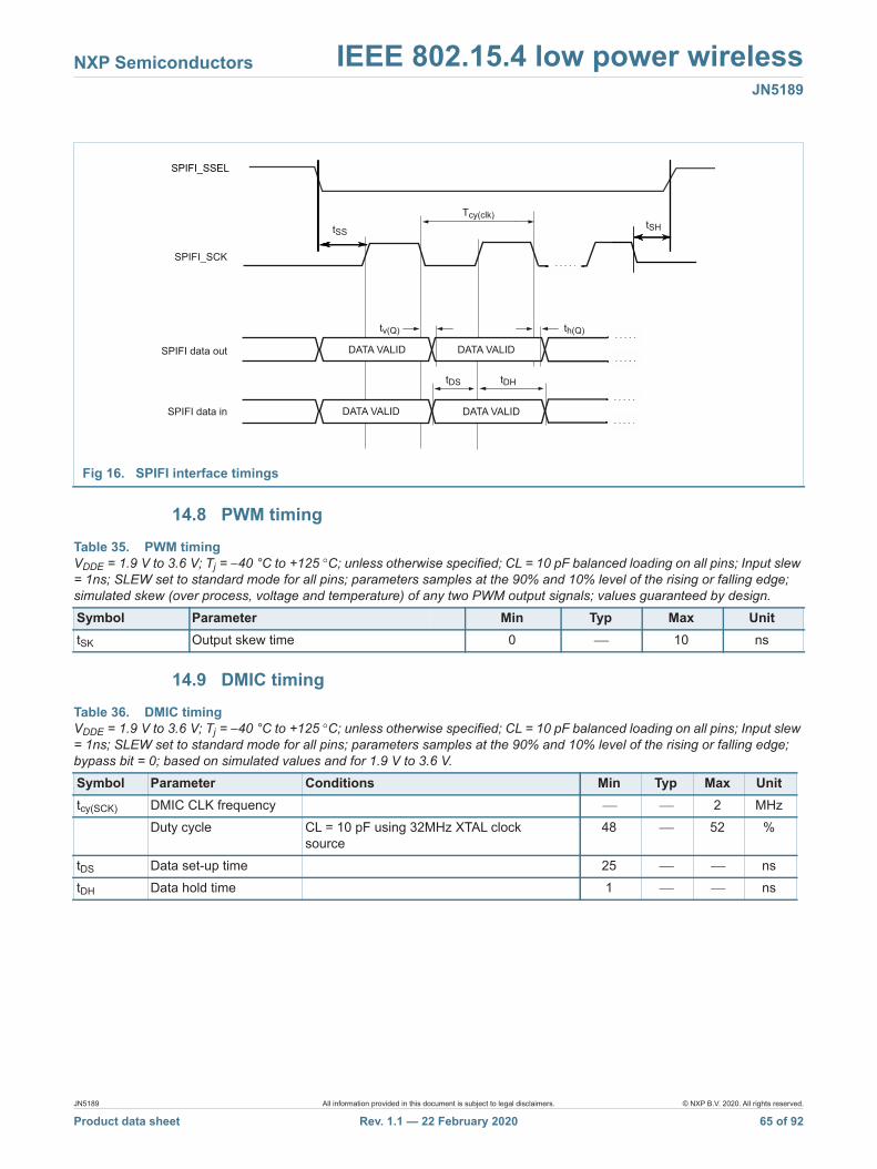
NXP Semiconductors IEEE 802.15.4 low power wirelessJN5189
14.8 PWM timing
14.9 DMIC timing
Fig 16. SPIFI interface timings
SPIFI_SCK
SPIFI data out
SPIFI data in
Tcy(clk)
tDS tDH
tv(Q)
DATA VALID DATA VALID
th(Q)
DATA VALID DATA VALID
SPIFI_SSEL
tSStSH
Table 35. PWM timingVDDE = 1.9 V to 3.6 V; Tj = −40 °C to +125 °C; unless otherwise specified; CL = 10 pF balanced loading on all pins; Input slew = 1ns; SLEW set to standard mode for all pins; parameters samples at the 90% and 10% level of the rising or falling edge; simulated skew (over process, voltage and temperature) of any two PWM output signals; values guaranteed by design.
Symbol Parameter Min Typ Max UnittSK Output skew time 0 10 ns
Table 36. DMIC timingVDDE = 1.9 V to 3.6 V; Tj = −40 °C to +125 °C; unless otherwise specified; CL = 10 pF balanced loading on all pins; Input slew = 1ns; SLEW set to standard mode for all pins; parameters samples at the 90% and 10% level of the rising or falling edge; bypass bit = 0; based on simulated values and for 1.9 V to 3.6 V.
Symbol Parameter Conditions Min Typ Max Unittcy(SCK) DMIC CLK frequency 2 MHz
Duty cycle CL = 10 pF using 32MHz XTAL clock source
48 52 %
tDS Data set-up time 25 nstDH Data hold time 1 ns
JN5189 All information provided in this document is subject to legal disclaimers. © NXP B.V. 2020. All rights reserved.
Product data sheet Rev. 1.1 — 22 February 2020 65 of 92

NXP Semiconductors IEEE 802.15.4 low power wirelessJN5189
14.10 ISO7816
Fig 17. DMIC interface timings
CLOCK
DATA
tSUtDH
Table 37. Clock of ISO7816VDDE = 1.9 V to 3.6 V; Tj = −40 °C to +125 °C; unless otherwise specified; guaranteed by design; Not tested in production.
Symbol Parameter Min Typ Max UnitVOH High-level output voltage 0.7 x VBAT VBAT VVOL Low-level output voltage 0 0.3 x VBAT V
Duty cycle 48 52 %Freq CLK frequency 2 12 MHz
Table 38. Input output of ISO7816VDDE = 1.9 V to 3.6 V; Tj = −40 °C to +125 °C; unless otherwise specified; guaranteed by design; Not tested in production.
Symbol Parameter Conditions Min Typ Max UnitVOH High-level output voltage CL = 10 pF 0.7 x VBAT VBAT VVOL Low-level output voltage CL = 10 pF 0 0.3 x VBAT VVIH High-level input voltage 0.75 x VBAT VBAT + 0.1 VVIL Low-level input voltage For VBAT from 0 V to 3.6 V 0 0.3 VIOH High-level output current 10 1000 AIOL Low-level output current 600 1000 Atr(O) Output rise time CL= 30 pF; 10 % to 90 %;
0 V to VBAT
1.2 s
tf(O) Output fall time CL= 30 pF; 10 % to 90 %;0 V to VBAT
1.2 s
tr(I) Input rise time 100 nstf(I) Input fall time 100 ns
JN5189 All information provided in this document is subject to legal disclaimers. © NXP B.V. 2020. All rights reserved.
Product data sheet Rev. 1.1 — 22 February 2020 66 of 92
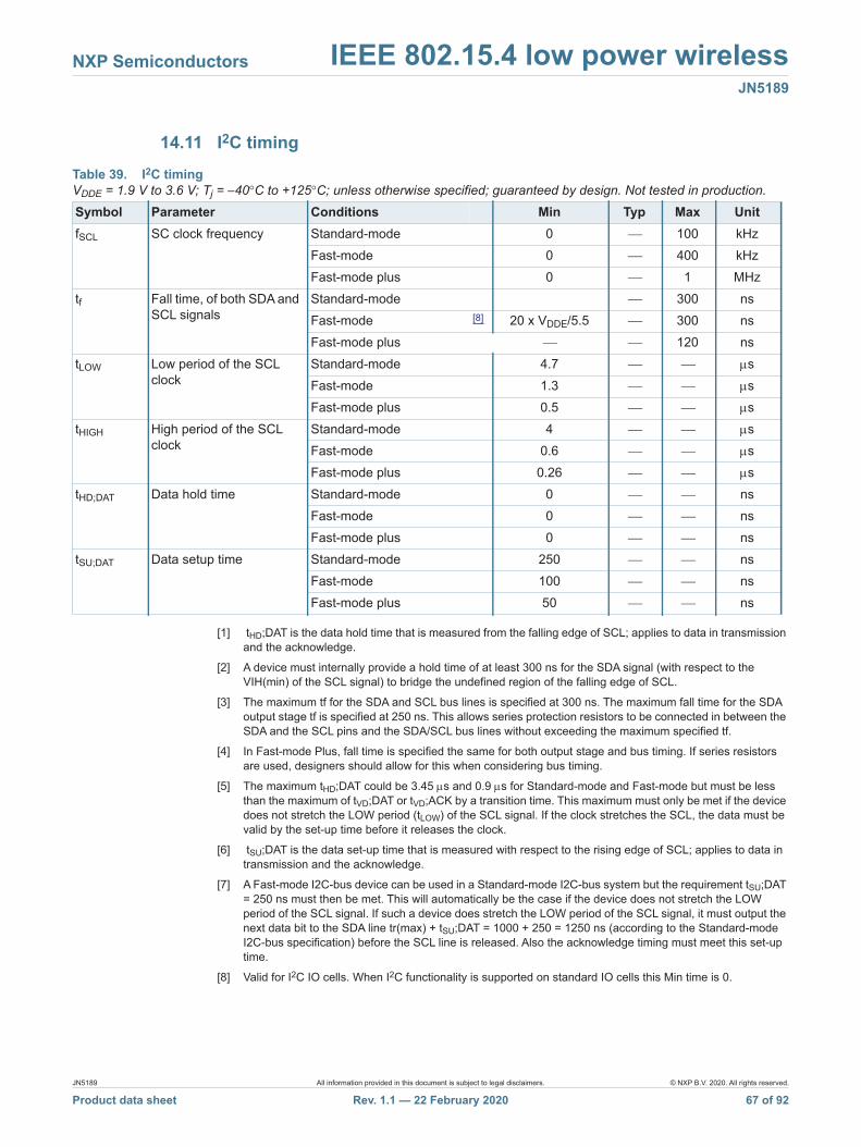
NXP Semiconductors IEEE 802.15.4 low power wirelessJN5189
14.11 I2C timing
[1] tHD;DAT is the data hold time that is measured from the falling edge of SCL; applies to data in transmission and the acknowledge.
[2] A device must internally provide a hold time of at least 300 ns for the SDA signal (with respect to the VIH(min) of the SCL signal) to bridge the undefined region of the falling edge of SCL.
[3] The maximum tf for the SDA and SCL bus lines is specified at 300 ns. The maximum fall time for the SDA output stage tf is specified at 250 ns. This allows series protection resistors to be connected in between the SDA and the SCL pins and the SDA/SCL bus lines without exceeding the maximum specified tf.
[4] In Fast-mode Plus, fall time is specified the same for both output stage and bus timing. If series resistors are used, designers should allow for this when considering bus timing.
[5] The maximum tHD;DAT could be 3.45 s and 0.9 s for Standard-mode and Fast-mode but must be less than the maximum of tVD;DAT or tVD;ACK by a transition time. This maximum must only be met if the device does not stretch the LOW period (tLOW) of the SCL signal. If the clock stretches the SCL, the data must be valid by the set-up time before it releases the clock.
[6] tSU;DAT is the data set-up time that is measured with respect to the rising edge of SCL; applies to data in transmission and the acknowledge.
[7] A Fast-mode I2C-bus device can be used in a Standard-mode I2C-bus system but the requirement tSU;DAT = 250 ns must then be met. This will automatically be the case if the device does not stretch the LOW period of the SCL signal. If such a device does stretch the LOW period of the SCL signal, it must output the next data bit to the SDA line tr(max) + tSU;DAT = 1000 + 250 = 1250 ns (according to the Standard-mode I2C-bus specification) before the SCL line is released. Also the acknowledge timing must meet this set-up time.
[8] Valid for I2C IO cells. When I2C functionality is supported on standard IO cells this Min time is 0.
Table 39. I2C timingVDDE = 1.9 V to 3.6 V; Tj = −40°C to +125°C; unless otherwise specified; guaranteed by design. Not tested in production.
Symbol Parameter Conditions Min Typ Max UnitfSCL SC clock frequency Standard-mode 0 100 kHz
Fast-mode 0 400 kHzFast-mode plus 0 1 MHz
tf Fall time, of both SDA and SCL signals
Standard-mode 300 nsFast-mode [8] 20 x VDDE/5.5 300 nsFast-mode plus 120 ns
tLOW Low period of the SCL clock
Standard-mode 4.7 sFast-mode 1.3 sFast-mode plus 0.5 s
tHIGH High period of the SCL clock
Standard-mode 4 sFast-mode 0.6 sFast-mode plus 0.26 s
tHD;DAT Data hold time Standard-mode 0 nsFast-mode 0 nsFast-mode plus 0 ns
tSU;DAT Data setup time Standard-mode 250 nsFast-mode 100 nsFast-mode plus 50 ns
JN5189 All information provided in this document is subject to legal disclaimers. © NXP B.V. 2020. All rights reserved.
Product data sheet Rev. 1.1 — 22 February 2020 67 of 92
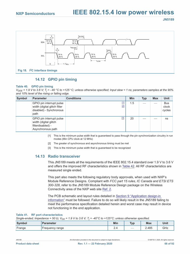
NXP Semiconductors IEEE 802.15.4 low power wirelessJN5189
14.12 GPIO pin timing
[1] This is the minimum pulse width that is guaranteed to pass through the pin synchronization circuitry in run modes (Min CPU clock at 12 MHz)
[2] The greater of synchronous and asynchronous timing must be met
[3] This is the minimum pulse width that is guaranteed to be recognized
14.13 Radio transceiverThis JN5189 meets all the requirements of the IEEE 802.15.4 standard over 1.9 V to 3.6 V and offers the improved RF characteristics shown in Table 42. All RF characteristics are measured single ended.
This part also meets the following regulatory body approvals, when used with NXP’s Module Reference Designs. Compliant with FCC part 15 rules, IC Canada and ETSI ETS 300-328, refer to the JN5189 Module Reference Design package on the Wireless Connectivity area of the NXP web site Ref. 2.
The PCB schematic and layout rules detailed in Section 9 “Application design-in information” must be followed. Failure to do so will likely result in the JN5189 failing to meet the performance specification detailed herein and worst case may result in device not functioning in the end application.
Fig 18. I2C interface timings
tf
70 %30 %SDA
tf
70 %30 %
S
70 %30 %
70 %30 %
tHD;DAT
SCL
1 / fSCL
70 %30 %
70 %30 %
tHIGH
tLOW
tSU;DAT
Table 40. GPIO pin timingVDDE = 1.9 V to 3.6 V; Tj = −40 °C to +125 °C; unless otherwise specified; Input slew = 1 ns; parameters samples at the 90% and 10% level of the rising or falling edge.
Symbol Parameter Conditions Min Typ Max UnitGPIO pin interrupt pulse width (digital glitch filter disabled) - Synchronous path
[1][2]
1.5 Bus clock cycles
GPIO pin interrupt pulse width (digital glitch filterdisabled) - Asynchronous path
[3] 20 ns
Table 41. RF port characteristics Single-ended; Impedance = 50 Ω; VDD = 1.9 V to 3.6 V; Tj = -40°C to +125°C; unless otherwise specified.
Symbol Parameter Min Typ Max UnitFrange Frequency range 2.4 2.485 GHz
JN5189 All information provided in this document is subject to legal disclaimers. © NXP B.V. 2020. All rights reserved.
Product data sheet Rev. 1.1 — 22 February 2020 68 of 92
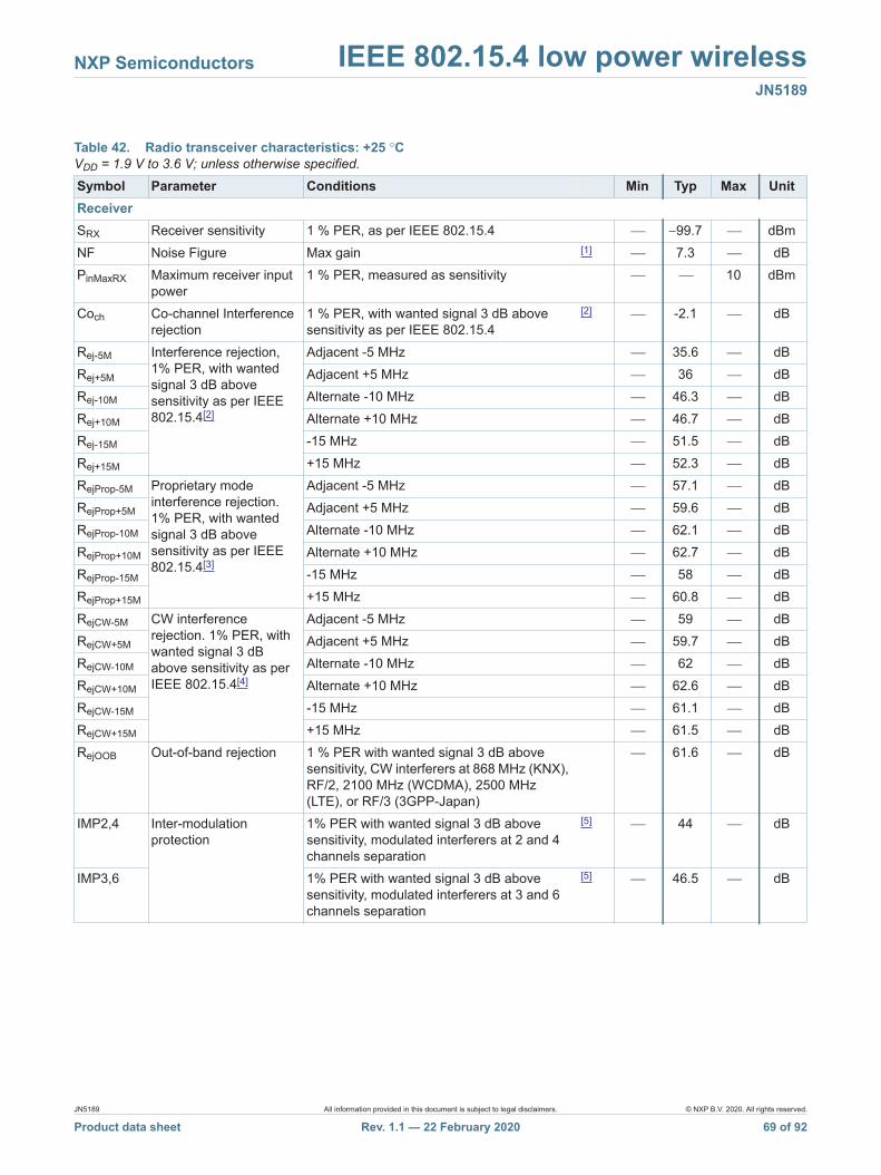
NXP Semiconductors IEEE 802.15.4 low power wirelessJN5189
Table 42. Radio transceiver characteristics: +25 °C VDD = 1.9 V to 3.6 V; unless otherwise specified.
Symbol Parameter Conditions Min Typ Max UnitReceiverSRX Receiver sensitivity 1 % PER, as per IEEE 802.15.4 99.7 dBmNF Noise Figure Max gain [1] 7.3 dBPinMaxRX Maximum receiver input
power1 % PER, measured as sensitivity 10 dBm
Coch Co-channel Interference rejection
1 % PER, with wanted signal 3 dB above sensitivity as per IEEE 802.15.4
[2] -2.1 dB
Rej-5M Interference rejection, 1% PER, with wanted signal 3 dB above sensitivity as per IEEE 802.15.4[2]
Adjacent -5 MHz 35.6 dBRej+5M Adjacent +5 MHz 36 dBRej-10M Alternate -10 MHz 46.3 dBRej+10M Alternate +10 MHz 46.7 dBRej-15M -15 MHz 51.5 dBRej+15M +15 MHz 52.3 dBRejProp-5M Proprietary mode
interference rejection. 1% PER, with wanted signal 3 dB above sensitivity as per IEEE 802.15.4[3]
Adjacent -5 MHz 57.1 dBRejProp+5M Adjacent +5 MHz 59.6 dBRejProp-10M Alternate -10 MHz 62.1 dBRejProp+10M Alternate +10 MHz 62.7 dBRejProp-15M -15 MHz 58 dBRejProp+15M +15 MHz 60.8 dBRejCW-5M CW interference
rejection. 1% PER, with wanted signal 3 dB above sensitivity as per IEEE 802.15.4[4]
Adjacent -5 MHz 59 dBRejCW+5M Adjacent +5 MHz 59.7 dBRejCW-10M Alternate -10 MHz 62 dBRejCW+10M Alternate +10 MHz 62.6 dBRejCW-15M -15 MHz 61.1 dBRejCW+15M +15 MHz 61.5 dBRejOOB Out-of-band rejection 1 % PER with wanted signal 3 dB above
sensitivity, CW interferers at 868 MHz (KNX), RF/2, 2100 MHz (WCDMA), 2500 MHz (LTE), or RF/3 (3GPP-Japan)
61.6 dB
IMP2,4 Inter-modulation protection
1% PER with wanted signal 3 dB above sensitivity, modulated interferers at 2 and 4 channels separation
[5] 44 dB
IMP3,6 1% PER with wanted signal 3 dB above sensitivity, modulated interferers at 3 and 6 channels separation
[5] 46.5 dB
JN5189 All information provided in this document is subject to legal disclaimers. © NXP B.V. 2020. All rights reserved.
Product data sheet Rev. 1.1 — 22 February 2020 69 of 92

NXP Semiconductors IEEE 802.15.4 low power wirelessJN5189
PinBlocking
Blocking input power Desired channel IEEE 802.15.4, level = measured sensitivity + 6dB, channels 11 & 26. Unwanted channel CW at 2380 MHz or 2503.5 MHz
-20.6 dBm
Desired channel IEEE 802.15.4, level = measured sensitivity + 6dB, channels 11 & 26. Unwanted channel CW at 2300 MHz, 2330 MHz & 2360 MHz
-19.5 dBm
Desired channel IEEE 802.15.4, level = measured sensitivity + 6dB, channels 11 & 26. Unwanted channel CW at 2523.5 MHz, 2553.5 MHZ, 2583.5 MHz, 2613.5 MHz, 2643.5 MHz, 2673.5 MHz
-18.7 dBm
RSSIvar RSSI variation Desired channel IEEE 802.15.4, over the RSSI range -100 dBm to 8 dBm
[6] 2 dB
PspRX Receiver spurious emission, measured conducted into 50 ohms
30 MHz to 1 GHz, 100 kHz RBW, 300 kHz VBW, Filter type 3 dB (Gaussian), Peak detector, Trace Mode Max hold
-87.1 dBm
1 GHz to 12.75 GHz, 1 MHz RBW, 3MHz VBW, Filter type 3dB (Gaussian), Peak detector, Trace mode Max hold
-70.9 dBm
LOLeakRX Local oscillator leakage power
-98 dBm
RejWIFI WIFI rejection 1% PER, with wanted signal IEEE 802.15.4 -75 dBm 2470 MHz, WIFI signal IEEE 802.11n 2447 MHz (20MHz mode)
55.6 dB
TransmitterPoutMax Maximum output power 11.2 dBmPout Output power +10 dBm
accuracyIn-band tilt 9.9
0.3 dBm
PoutRange Output power control range
45.7 dB
EVM Error vector magnitude With IEEE 802.15.4 channel at +10 dBm 6.3 %OEVM Offset error vector
magnitude With IEEE 802.15.4 channel at +10 dBm 0.33 %
EVMProp Error Vector Magnitude With proprietary mode at +10 dBm 23.2 %OEVMProp Offset error Vector
MagnitudeWith proprietary mode at +10 dBm 3.2 %
PSD Power spectral density Relative density at greater than 3.5 MHz offset as per IEEE 802.15.4 at +10 dBm
-37.4 dBc
Absolute density at greater than 3.5 MHz offset at +10 dBm as per IEEE 802.15.4 at +10 dBm
-38.2 dBm
PSDProp Proprietary mode power spectral density
Relative density at greater than 3.5 MHz offset with proprietary mode at +10 dBm
-61.2 dBc
Absolute density at greater than 3.5 MHz offset with proprietary mode at +10 dBm
-62.2 dBm
Table 42. Radio transceiver characteristics: +25 °C …continuedVDD = 1.9 V to 3.6 V; unless otherwise specified.
Symbol Parameter Conditions Min Typ Max Unit
JN5189 All information provided in this document is subject to legal disclaimers. © NXP B.V. 2020. All rights reserved.
Product data sheet Rev. 1.1 — 22 February 2020 70 of 92
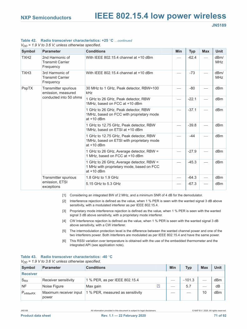
NXP Semiconductors IEEE 802.15.4 low power wirelessJN5189
[1] Considering an integrated BW of 2 MHz, and a minimum SNR of 4 dB for the demodulator.
[2] Interference rejection is defined as the value, when 1 % PER is seen with the wanted signal 3 dB above sensitivity, with a modulated interferer as per IEEE 802.15.4.
[3] Proprietary mode interference rejection is defined as the value, when 1 % PER is seen with the wanted signal 3 dB above sensitivity, with a proprietary mode interferer.
[4] CW Interference rejection is defined as the value, when 1 % PER is seen with the wanted signal 3 dB above sensitivity, with a CW interferer.
[5] The intermodulation protection level is the difference between the wanted channel power and one of the two interferers power. Both interferers are modulated as per IEEE 802.15.4 and have the same power.
[6] This RSSI variation over temperature is obtained with the use of the embedded thermometer and the integrated API (see application note).
TXH2 2nd Harmonic of Transmit Carrier Frequency
With IEEE 802.15.4 channel at +10 dBm -62.4 dBm/MHz
TXH3 3rd Harmonic of Transmit Carrier Frequency
With IEEE 802.15.4 channel at +10 dBm -73 dBm/MHz
PspTX Transmitter spurious emission, measured conducted into 50 ohms
30 MHz to 1 GHz, Peak detector, RBW=100 kHz
-80 dBm
1 GHz to 26 GHz, Peak detector, RBW 1MHz, based on FCC at +10 dBm
-22.1 dBm
1 GHz to 26 GHz, Peak detector, RBW 1MHz, based on FCC with proprietary mode at +10 dBm
-37.1 dBm
1 GHz to 12.75 GHz, Peak detector, RBW 1MHz, based on ETSI at +10 dBm
-39.8 dBm
1 GHz to 12.75 GHz, Peak detector, RBW 1MHz, based on ETSI with proprietary mode at +10 dBm
-44 dBm
1 GHz to 26 GHz, Average detector, RBW = 1 MHz, based on FCC at +10 dBm
-27.9 dBm
1 GHz to 26 GHz, Average detector, RBW = 1 MHz with proprietary mode, based on FCC at +10 dBm
-45.3 dBm
Transmitter spurious emission, ETSI exceptions
1.8 GHz to 1.9 GHz -64.3 dBm5.15 GHz to 5.3 GHz -67.3 dBm
Table 42. Radio transceiver characteristics: +25 °C …continuedVDD = 1.9 V to 3.6 V; unless otherwise specified.
Symbol Parameter Conditions Min Typ Max Unit
Table 43. Radio transceiver characteristics: -40 °C VDD = 1.9 V to 3.6 V; unless otherwise specified.
Symbol Parameter Conditions Min Typ Max UnitReceiverSRX Receiver sensitivity 1 % PER, as per IEEE 802.15.4 101.3 dBmNF Noise Figure Max gain [1] 5.7 dBPinMaxRX Maximum receiver input
power1 % PER, measured as sensitivity 10 dBm
JN5189 All information provided in this document is subject to legal disclaimers. © NXP B.V. 2020. All rights reserved.
Product data sheet Rev. 1.1 — 22 February 2020 71 of 92
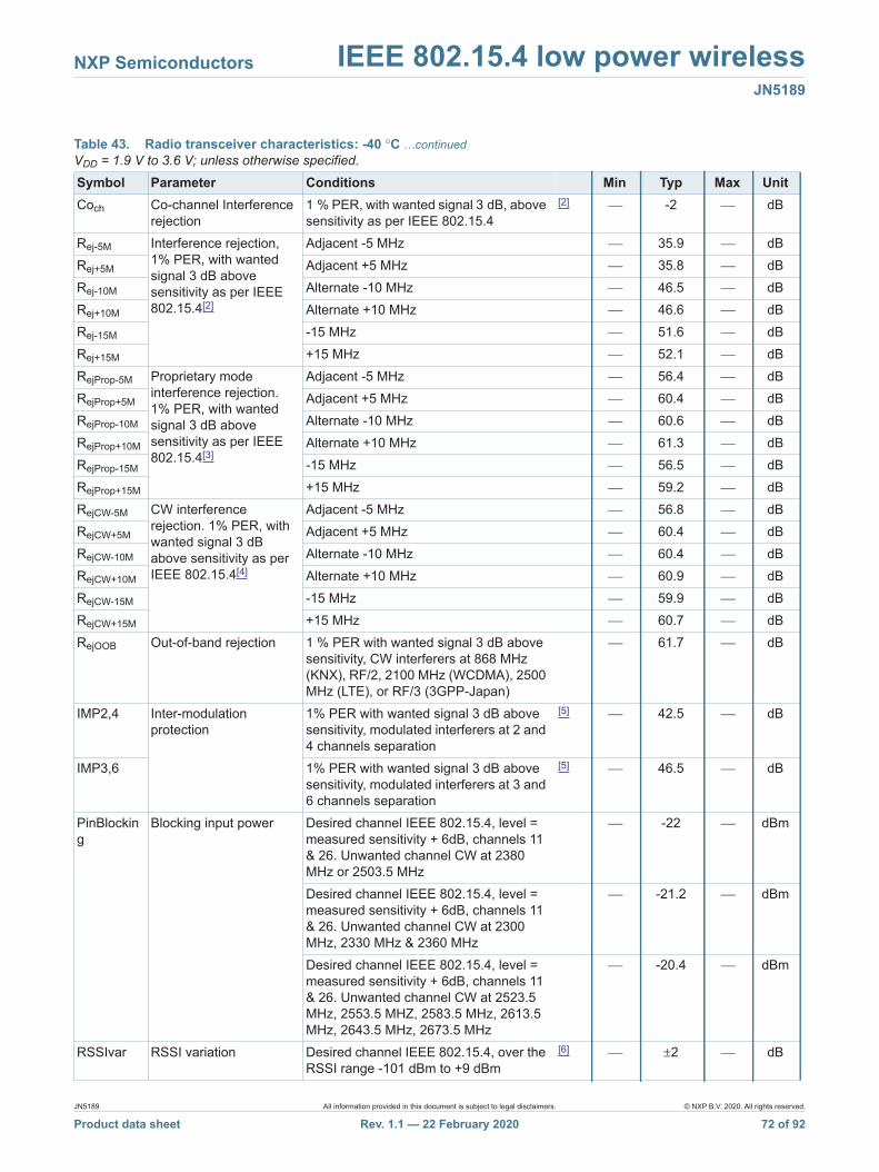
NXP Semiconductors IEEE 802.15.4 low power wirelessJN5189
Coch Co-channel Interference rejection
1 % PER, with wanted signal 3 dB, above sensitivity as per IEEE 802.15.4
[2] -2 dB
Rej-5M Interference rejection, 1% PER, with wanted signal 3 dB above sensitivity as per IEEE 802.15.4[2]
Adjacent -5 MHz 35.9 dBRej+5M Adjacent +5 MHz 35.8 dBRej-10M Alternate -10 MHz 46.5 dBRej+10M Alternate +10 MHz 46.6 dBRej-15M -15 MHz 51.6 dBRej+15M +15 MHz 52.1 dBRejProp-5M Proprietary mode
interference rejection. 1% PER, with wanted signal 3 dB above sensitivity as per IEEE 802.15.4[3]
Adjacent -5 MHz 56.4 dBRejProp+5M Adjacent +5 MHz 60.4 dBRejProp-10M Alternate -10 MHz 60.6 dBRejProp+10M Alternate +10 MHz 61.3 dBRejProp-15M -15 MHz 56.5 dBRejProp+15M +15 MHz 59.2 dBRejCW-5M CW interference
rejection. 1% PER, with wanted signal 3 dB above sensitivity as per IEEE 802.15.4[4]
Adjacent -5 MHz 56.8 dBRejCW+5M Adjacent +5 MHz 60.4 dBRejCW-10M Alternate -10 MHz 60.4 dBRejCW+10M Alternate +10 MHz 60.9 dBRejCW-15M -15 MHz 59.9 dBRejCW+15M +15 MHz 60.7 dBRejOOB Out-of-band rejection 1 % PER with wanted signal 3 dB above
sensitivity, CW interferers at 868 MHz (KNX), RF/2, 2100 MHz (WCDMA), 2500 MHz (LTE), or RF/3 (3GPP-Japan)
61.7 dB
IMP2,4 Inter-modulation protection
1% PER with wanted signal 3 dB above sensitivity, modulated interferers at 2 and 4 channels separation
[5] 42.5 dB
IMP3,6 1% PER with wanted signal 3 dB above sensitivity, modulated interferers at 3 and 6 channels separation
[5] 46.5 dB
PinBlocking
Blocking input power Desired channel IEEE 802.15.4, level = measured sensitivity + 6dB, channels 11 & 26. Unwanted channel CW at 2380 MHz or 2503.5 MHz
-22 dBm
Desired channel IEEE 802.15.4, level = measured sensitivity + 6dB, channels 11 & 26. Unwanted channel CW at 2300 MHz, 2330 MHz & 2360 MHz
-21.2 dBm
Desired channel IEEE 802.15.4, level = measured sensitivity + 6dB, channels 11 & 26. Unwanted channel CW at 2523.5 MHz, 2553.5 MHZ, 2583.5 MHz, 2613.5 MHz, 2643.5 MHz, 2673.5 MHz
-20.4 dBm
RSSIvar RSSI variation Desired channel IEEE 802.15.4, over the RSSI range -101 dBm to +9 dBm
[6] 2 dB
Table 43. Radio transceiver characteristics: -40 °C …continuedVDD = 1.9 V to 3.6 V; unless otherwise specified.
Symbol Parameter Conditions Min Typ Max Unit
JN5189 All information provided in this document is subject to legal disclaimers. © NXP B.V. 2020. All rights reserved.
Product data sheet Rev. 1.1 — 22 February 2020 72 of 92
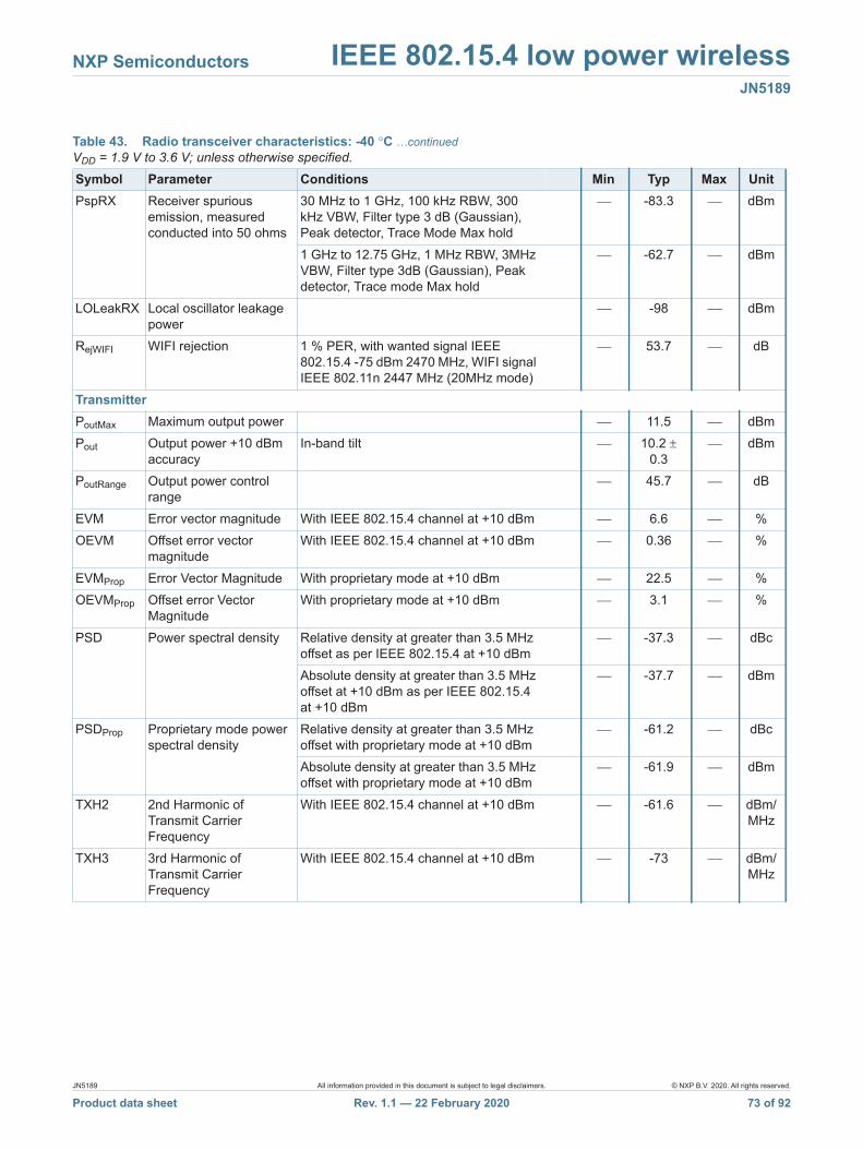
NXP Semiconductors IEEE 802.15.4 low power wirelessJN5189
PspRX Receiver spurious emission, measured conducted into 50 ohms
30 MHz to 1 GHz, 100 kHz RBW, 300 kHz VBW, Filter type 3 dB (Gaussian), Peak detector, Trace Mode Max hold
-83.3 dBm
1 GHz to 12.75 GHz, 1 MHz RBW, 3MHz VBW, Filter type 3dB (Gaussian), Peak detector, Trace mode Max hold
-62.7 dBm
LOLeakRX Local oscillator leakage power
-98 dBm
RejWIFI WIFI rejection 1 % PER, with wanted signal IEEE 802.15.4 -75 dBm 2470 MHz, WIFI signal IEEE 802.11n 2447 MHz (20MHz mode)
53.7 dB
TransmitterPoutMax Maximum output power 11.5 dBmPout Output power +10 dBm
accuracyIn-band tilt 10.2
0.3 dBm
PoutRange Output power control range
45.7 dB
EVM Error vector magnitude With IEEE 802.15.4 channel at +10 dBm 6.6 %OEVM Offset error vector
magnitude With IEEE 802.15.4 channel at +10 dBm 0.36 %
EVMProp Error Vector Magnitude With proprietary mode at +10 dBm 22.5 %OEVMProp Offset error Vector
MagnitudeWith proprietary mode at +10 dBm 3.1 %
PSD Power spectral density Relative density at greater than 3.5 MHz offset as per IEEE 802.15.4 at +10 dBm
-37.3 dBc
Absolute density at greater than 3.5 MHz offset at +10 dBm as per IEEE 802.15.4 at +10 dBm
-37.7 dBm
PSDProp Proprietary mode power spectral density
Relative density at greater than 3.5 MHz offset with proprietary mode at +10 dBm
-61.2 dBc
Absolute density at greater than 3.5 MHz offset with proprietary mode at +10 dBm
-61.9 dBm
TXH2 2nd Harmonic of Transmit Carrier Frequency
With IEEE 802.15.4 channel at +10 dBm -61.6 dBm/MHz
TXH3 3rd Harmonic of Transmit Carrier Frequency
With IEEE 802.15.4 channel at +10 dBm -73 dBm/MHz
Table 43. Radio transceiver characteristics: -40 °C …continuedVDD = 1.9 V to 3.6 V; unless otherwise specified.
Symbol Parameter Conditions Min Typ Max Unit
JN5189 All information provided in this document is subject to legal disclaimers. © NXP B.V. 2020. All rights reserved.
Product data sheet Rev. 1.1 — 22 February 2020 73 of 92
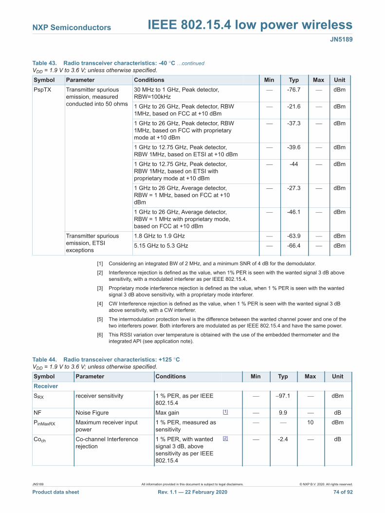
NXP Semiconductors IEEE 802.15.4 low power wirelessJN5189
[1] Considering an integrated BW of 2 MHz, and a minimum SNR of 4 dB for the demodulator.
[2] Interference rejection is defined as the value, when 1% PER is seen with the wanted signal 3 dB above sensitivity, with a modulated interferer as per IEEE 802.15.4.
[3] Proprietary mode interference rejection is defined as the value, when 1 % PER is seen with the wanted signal 3 dB above sensitivity, with a proprietary mode interferer.
[4] CW Interference rejection is defined as the value, when 1 % PER is seen with the wanted signal 3 dB above sensitivity, with a CW interferer.
[5] The intermodulation protection level is the difference between the wanted channel power and one of the two interferers power. Both interferers are modulated as per IEEE 802.15.4 and have the same power.
[6] This RSSI variation over temperature is obtained with the use of the embedded thermometer and the integrated API (see application note).
PspTX Transmitter spurious emission, measured conducted into 50 ohms
30 MHz to 1 GHz, Peak detector, RBW=100kHz
-76.7 dBm
1 GHz to 26 GHz, Peak detector, RBW 1MHz, based on FCC at +10 dBm
-21.6 dBm
1 GHz to 26 GHz, Peak detector, RBW 1MHz, based on FCC with proprietary mode at +10 dBm
-37.3 dBm
1 GHz to 12.75 GHz, Peak detector, RBW 1MHz, based on ETSI at +10 dBm
-39.6 dBm
1 GHz to 12.75 GHz, Peak detector, RBW 1MHz, based on ETSI with proprietary mode at +10 dBm
-44 dBm
1 GHz to 26 GHz, Average detector, RBW = 1 MHz, based on FCC at +10 dBm
-27.3 dBm
1 GHz to 26 GHz, Average detector, RBW = 1 MHz with proprietary mode, based on FCC at +10 dBm
-46.1 dBm
Transmitter spurious emission, ETSI exceptions
1.8 GHz to 1.9 GHz -63.9 dBm5.15 GHz to 5.3 GHz -66.4 dBm
Table 43. Radio transceiver characteristics: -40 °C …continuedVDD = 1.9 V to 3.6 V; unless otherwise specified.
Symbol Parameter Conditions Min Typ Max Unit
Table 44. Radio transceiver characteristics: +125 °C VDD = 1.9 V to 3.6 V; unless otherwise specified.
Symbol Parameter Conditions Min Typ Max UnitReceiverSRX receiver sensitivity 1 % PER, as per IEEE
802.15.4 97.1 dBm
NF Noise Figure Max gain [1] 9.9 dBPinMaxRX Maximum receiver input
power1 % PER, measured as sensitivity
10 dBm
Coch Co-channel Interference rejection
1 % PER, with wanted signal 3 dB, above sensitivity as per IEEE 802.15.4
[2] -2.4 dB
JN5189 All information provided in this document is subject to legal disclaimers. © NXP B.V. 2020. All rights reserved.
Product data sheet Rev. 1.1 — 22 February 2020 74 of 92

NXP Semiconductors IEEE 802.15.4 low power wirelessJN5189
Rej-5M Interference rejection, 1% PER, with wanted signal 3 dB above sensitivity as per IEEE 802.15.4[2]
Adjacent -5 MHz 35.4 dBRej+5M Adjacent +5 MHz 35.8 dBRej-10M Alternate -10 MHz 46.3 dBRej+10M Alternate +10 MHz 46.5 dBRej-15M -15 MHz 51.7 dBRej+15M +15 MHz 52.1 dBRejProp-5M Proprietary mode
interference rejection. 1% PER, with wanted signal 3 dB above sensitivity as per IEEE 802.15.4[3]
Adjacent -5 MHz 54.7 dBRejProp+5M Adjacent +5 MHz 56.8 dBRejProp-10M Alternate -10 MHz 59.9 dBRejProp+10M Alternate +10 MHz 63.3 dBRejProp-15M -15 MHz 60.3 dBRejProp+15M +15 MHz 65.4 dBRejCW-5M CW interference rejection.
1% PER, with wanted signal 3 dB above sensitivity as per IEEE 802.15.4[4]
Adjacent -5 MHz 56.1 dBRejCW+5M Adjacent +5 MHz 57.6 dBRejCW-10M Alternate -10 MHz 62.9 dBRejCW+10M Alternate +10 MHz 64 dBRejCW-15M -15 MHz 62.3 dBRejCW+15M +15 MHz 65.3 dBRejOOB Out-of-band rejection 1 % PER with wanted
signal 3 dB above sensitivity, CW interferers at 868 MHz (KNX), RF/2, 2100 MHz (WCDMA), 2500 MHz (LTE), or RF/3 (3GPP-Japan)
60.8 dB
IMP2,4 Inter-modulation protection 1% PER with wanted signal 3 dB above sensitivity, modulated interferers at 2 and 4 channels separation
[5] 44.8 dB
IMP3,6 1% PER with wanted signal 3 dB above sensitivity, modulated interferers at 3 and 6 channels separation
[5] 47 dB
Table 44. Radio transceiver characteristics: +125 °C …continuedVDD = 1.9 V to 3.6 V; unless otherwise specified.
Symbol Parameter Conditions Min Typ Max Unit
JN5189 All information provided in this document is subject to legal disclaimers. © NXP B.V. 2020. All rights reserved.
Product data sheet Rev. 1.1 — 22 February 2020 75 of 92
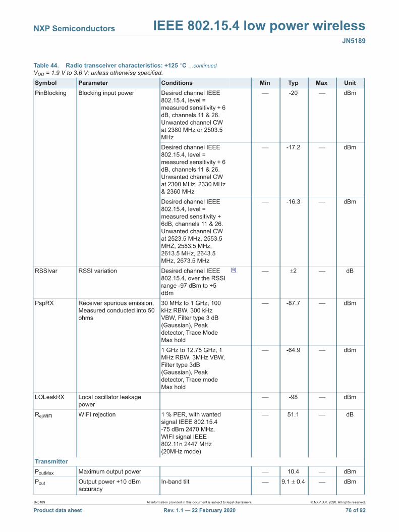
NXP Semiconductors IEEE 802.15.4 low power wirelessJN5189
PinBlocking Blocking input power Desired channel IEEE 802.15.4, level = measured sensitivity + 6 dB, channels 11 & 26. Unwanted channel CW at 2380 MHz or 2503.5 MHz
-20 dBm
Desired channel IEEE 802.15.4, level = measured sensitivity + 6 dB, channels 11 & 26. Unwanted channel CW at 2300 MHz, 2330 MHz & 2360 MHz
-17.2 dBm
Desired channel IEEE 802.15.4, level = measured sensitivity + 6dB, channels 11 & 26. Unwanted channel CW at 2523.5 MHz, 2553.5 MHZ, 2583.5 MHz, 2613.5 MHz, 2643.5 MHz, 2673.5 MHz
-16.3 dBm
RSSIvar RSSI variation Desired channel IEEE 802.15.4, over the RSSI range -97 dBm to +5 dBm
[6] 2 dB
PspRX Receiver spurious emission, Measured conducted into 50 ohms
30 MHz to 1 GHz, 100 kHz RBW, 300 kHz VBW, Filter type 3 dB (Gaussian), Peak detector, Trace Mode Max hold
-87.7 dBm
1 GHz to 12.75 GHz, 1 MHz RBW, 3MHz VBW, Filter type 3dB (Gaussian), Peak detector, Trace mode Max hold
-64.9 dBm
LOLeakRX Local oscillator leakage power
-98 dBm
RejWIFI WIFI rejection 1 % PER, with wanted signal IEEE 802.15.4 -75 dBm 2470 MHz, WIFI signal IEEE 802.11n 2447 MHz (20MHz mode)
51.1 dB
TransmitterPoutMax Maximum output power 10.4 dBmPout Output power +10 dBm
accuracyIn-band tilt 9.1 0.4 dBm
Table 44. Radio transceiver characteristics: +125 °C …continuedVDD = 1.9 V to 3.6 V; unless otherwise specified.
Symbol Parameter Conditions Min Typ Max Unit
JN5189 All information provided in this document is subject to legal disclaimers. © NXP B.V. 2020. All rights reserved.
Product data sheet Rev. 1.1 — 22 February 2020 76 of 92
NXP Semiconductors IEEE 802.15.4 low power wirelessJN5189
PoutRange Output power control range 46 dBEVM Error vector magnitude With IEEE 802.15.4
channel at +10 dBm 6.6 %
OEVM Offset error vector magnitude With IEEE 802.15.4 channel at +10 dBm
0.36 %
EVMProp Error Vector Magnitude With proprietary mode at +10 dBm
23 %
OEVMProp Offset error Vector Magnitude With proprietary mode at +10 dBm
3.2 %
PSD Power spectral density Relative density at greater than 3.5 MHz offset as per IEEE 802.15.4 at +10 dBm
-37.5 dBc
Absolute density at greater than 3.5 MHz offset at +10 dBm as per IEEE 802.15.4 at +10 dBm
-39.5 dBm
PSDProp Proprietary mode power spectral density
Relative density at greater than 3.5 MHz offset with proprietary mode at +10 dBm
-60.6 dBc
Absolute density at greater than 3.5 MHz offset with proprietary mode at +10 dBm
-62.8 dBm
TXH2 2nd Harmonic of Transmit Carrier Frequency
With IEEE 802.15.4 channel at +10 dBm
-63.3 dBm/MHz
TXH3 3rd Harmonic of Transmit Carrier Frequency
With IEEE 802.15.4 channel at +10 dBm
-73 dBm/MHz
Table 44. Radio transceiver characteristics: +125 °C …continuedVDD = 1.9 V to 3.6 V; unless otherwise specified.
Symbol Parameter Conditions Min Typ Max Unit
JN5189 All information provided in this document is subject to legal disclaimers. © NXP B.V. 2020. All rights reserved.
Product data sheet Rev. 1.1 — 22 February 2020 77 of 92
NXP Semiconductors IEEE 802.15.4 low power wirelessJN5189
[1] Considering an integrated BW of 2 MHz, and a minimum SNR of 4 dB for the demodulator.
[2] Interference rejection is defined as the value, when 1 % PER is seen with the wanted signal 3 dB above sensitivity, with a modulated interferer as per IEEE 802.15.4.
[3] Proprietary mode interference rejection is defined as the value, when 1 % PER is seen with the wanted signal 3 dB above sensitivity, with a proprietary mode interferer.
[4] CW Interference rejection is defined as the value, when 1 % PER is seen with the wanted signal 3 dB above sensitivity, with a CW interferer.
[5] The intermodulation protection level is the difference between the wanted channel power and one of the two interferers power. Both interferers are modulated as per IEEE 802.15.4 and have the same power.
[6] This RSSI variation over temperature is obtained with the use of the embedded thermometer and the integrated API (see application note).
PspTX Transmitter spurious emission, measured conducted into 50 ohms
30 MHz to 1 GHz, Peak detector, RBW=100kHz
-76.3 dBm
1 GHz to 26 GHz, Peak detector, RBW 1MHz, based on FCC at +10 dBm
-23.3 dBm
1 GHz to 26 GHz, Peak detector, RBW 1MHz, based on FCC with proprietary mode at +10 dBm
-39 dBm
1 GHz to 12.75 GHz, Peak detector, RBW 1MHz, based on ETSI at +10 dBm
-41.3 dBm
1 GHz to 12.75 GHz, Peak detector, RBW 1MHz, based on ETSI with proprietary mode at +10 dBm
-44.3 dBm
1 GHz to 26 GHz, Average detector, RBW = 1 MHz, based on FCC at +10 dBm
-29.2 dBm
1 GHz to 26 GHz, Average detector, RBW = 1 MHz with proprietary mode, based on FCC at +10 dBm
-46.3 dBm
Transmitter spurious emission, ETSI exceptions
1.8 GHz to 1.9 GHz -64.7 dBm5.15 GHz to 5.3 GHz -67.1 dBm
Table 44. Radio transceiver characteristics: +125 °C …continuedVDD = 1.9 V to 3.6 V; unless otherwise specified.
Symbol Parameter Conditions Min Typ Max Unit
JN5189 All information provided in this document is subject to legal disclaimers. © NXP B.V. 2020. All rights reserved.
Product data sheet Rev. 1.1 — 22 February 2020 78 of 92
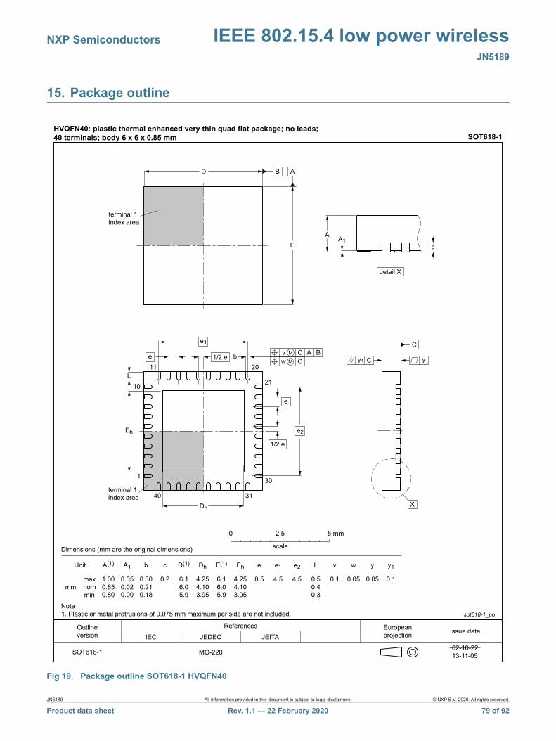
NXP Semiconductors IEEE 802.15.4 low power wirelessJN5189
15. Package outline
Fig 19. Package outline SOT618-1 HVQFN40
JN5189 All information provided in this document is subject to legal disclaimers. © NXP B.V. 2020. All rights reserved.
Product data sheet Rev. 1.1 — 22 February 2020 79 of 92
NXP Semiconductors IEEE 802.15.4 low power wirelessJN5189
16. Soldering of SMD packages
This text provides a very brief insight into a complex technology. A more in-depth account of soldering ICs can be found in Application Note AN10365 “Surface mount reflow soldering description”.
16.1 Introduction to solderingSoldering is one of the most common methods through which packages are attached to Printed Circuit Boards (PCBs), to form electrical circuits. The soldered joint provides both the mechanical and the electrical connection. There is no single soldering method that is ideal for all IC packages. Wave soldering is often preferred when through-hole and Surface Mount Devices (SMDs) are mixed on one printed wiring board; however, it is not suitable for fine pitch SMDs. Reflow soldering is ideal for the small pitches and high densities that come with increased miniaturization.
16.2 Wave and reflow solderingWave soldering is a joining technology in which the joints are made by solder coming from a standing wave of liquid solder. The wave soldering process is suitable for the following:
• Through-hole components• Leaded or leadless SMDs, which are glued to the surface of the printed circuit board
Not all SMDs can be wave soldered. Packages with solder balls, and some leadless packages which have solder lands underneath the body, cannot be wave soldered. Also, leaded SMDs with leads having a pitch smaller than ~0.6 mm cannot be wave soldered, due to an increased probability of bridging.
The reflow soldering process involves applying solder paste to a board, followed by component placement and exposure to a temperature profile. Leaded packages, packages with solder balls, and leadless packages are all reflow solderable.
Key characteristics in both wave and reflow soldering are:
• Board specifications, including the board finish, solder masks and vias• Package footprints, including solder thieves and orientation• The moisture sensitivity level of the packages• Package placement• Inspection and repair• Lead-free soldering versus SnPb soldering
16.3 Wave solderingKey characteristics in wave soldering are:
• Process issues, such as application of adhesive and flux, clinching of leads, board transport, the solder wave parameters, and the time during which components are exposed to the wave
• Solder bath specifications, including temperature and impurities
JN5189 All information provided in this document is subject to legal disclaimers. © NXP B.V. 2020. All rights reserved.
Product data sheet Rev. 1.1 — 22 February 2020 80 of 92
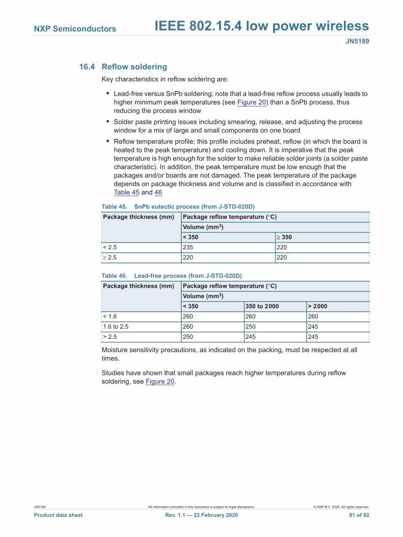
NXP Semiconductors IEEE 802.15.4 low power wirelessJN5189
16.4 Reflow solderingKey characteristics in reflow soldering are:
• Lead-free versus SnPb soldering; note that a lead-free reflow process usually leads to higher minimum peak temperatures (see Figure 20) than a SnPb process, thus reducing the process window
• Solder paste printing issues including smearing, release, and adjusting the process window for a mix of large and small components on one board
• Reflow temperature profile; this profile includes preheat, reflow (in which the board is heated to the peak temperature) and cooling down. It is imperative that the peak temperature is high enough for the solder to make reliable solder joints (a solder paste characteristic). In addition, the peak temperature must be low enough that the packages and/or boards are not damaged. The peak temperature of the package depends on package thickness and volume and is classified in accordance with Table 45 and 46
Moisture sensitivity precautions, as indicated on the packing, must be respected at all times.
Studies have shown that small packages reach higher temperatures during reflow soldering, see Figure 20.
Table 45. SnPb eutectic process (from J-STD-020D) Package thickness (mm) Package reflow temperature (°C)
Volume (mm3)< 350 ≥ 350
< 2.5 235 220 2.5 220 220
Table 46. Lead-free process (from J-STD-020D) Package thickness (mm) Package reflow temperature (°C)
Volume (mm3)< 350 350 to 2 000 > 2 000
< 1.6 260 260 2601.6 to 2.5 260 250 245> 2.5 250 245 245
JN5189 All information provided in this document is subject to legal disclaimers. © NXP B.V. 2020. All rights reserved.
Product data sheet Rev. 1.1 — 22 February 2020 81 of 92
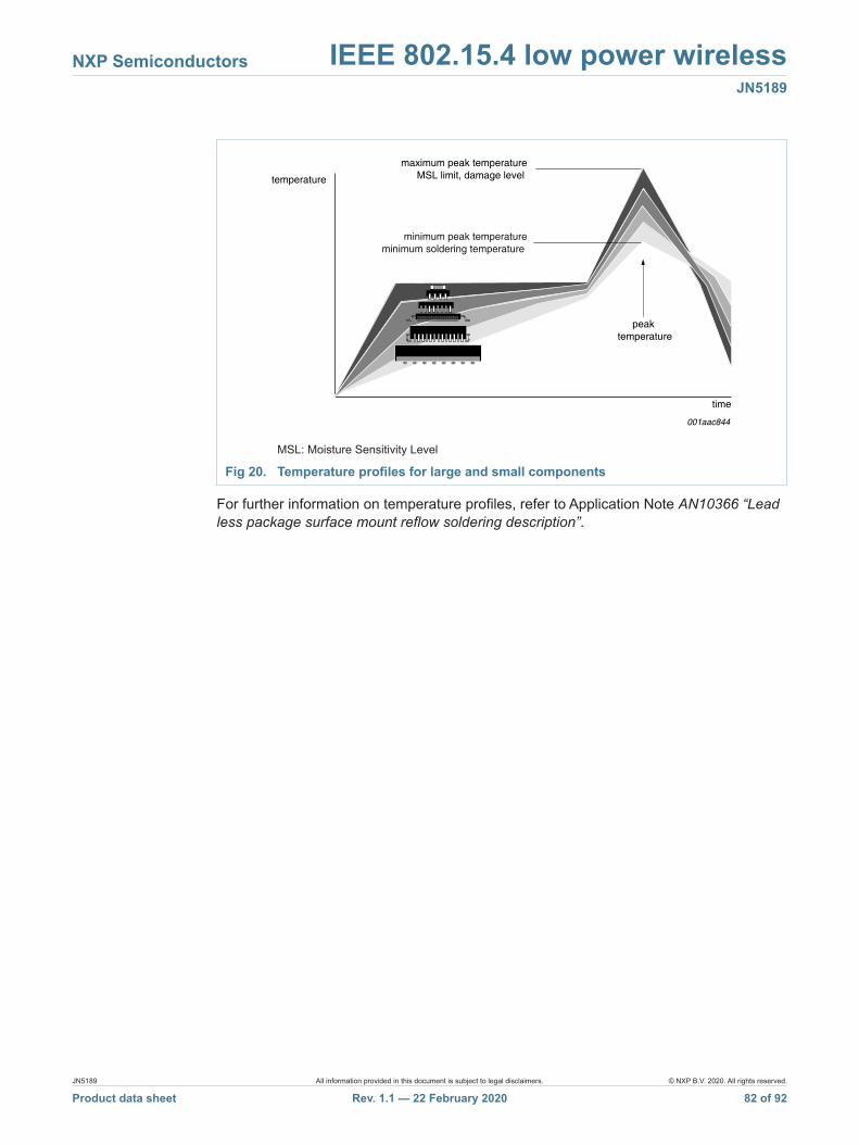
NXP Semiconductors IEEE 802.15.4 low power wirelessJN5189
For further information on temperature profiles, refer to Application Note AN10366 “Lead less package surface mount reflow soldering description”.
MSL: Moisture Sensitivity Level
Fig 20. Temperature profiles for large and small components
001aac844
temperature�
time
minimum peak temperature�� minimum soldering temperature
maximum peak temperature�� MSL limit, damage level
peak� temperature
JN5189 All information provided in this document is subject to legal disclaimers. © NXP B.V. 2020. All rights reserved.
Product data sheet Rev. 1.1 — 22 February 2020 82 of 92
NXP Semiconductors IEEE 802.15.4 low power wirelessJN5189
17. Abbreviations
Table 47. Abbreviations Acronym DescriptionADC Analog to Digital ConverterADE Antenna diversity EvenADO Antenna diversity OddAES Advanced Encryption StandardAGC Automatic Gain ControlAPI Application Program InterfaceAPT Analog Peripheral TimerBOM Bill Of MaterialBOR Brown-Out ResetCCA Clear Channel AssessmentCCM Counter with CBC-MACCDM Charged Device ModelCLK CLocKCPU Central Processing UnitCRC Cyclic redundancy CheckCSMA/CA Carrier Sense Multiple Access with Collision AvoidanceCTS Clear-To-SendCW Continuous WaveDALI Digitally Addressable Lighting InterfaceDC Direct currentDIO Digital Input OutputDMA Direct memory AccessDO Digital OutputED Energy DetectionEEPROM Electrically-Erasable Programmable Read Only MemoryESR Equivalent Series ResistanceFIFO First In First OutGP General PurposeGPIO General Purpose Input OutputHBM Human Body ModelHS High SpeedHVQFN Heatsink Very-thin Quad Flat No-LeadsID IDentificationIF Intermediate frequencyIO Input OutputIPC Interconnecting and Packaging Electronic CircuitsJTAG Joint Test Action GroupLNA Low Noise AmplifierLQI Link Quality Indication
JN5189 All information provided in this document is subject to legal disclaimers. © NXP B.V. 2020. All rights reserved.
Product data sheet Rev. 1.1 — 22 February 2020 83 of 92
NXP Semiconductors IEEE 802.15.4 low power wirelessJN5189
LSB Low Significant BitMAC Media Access ControlMSB Most Significant BitMSIF Master Serial InterFaceMSL Moisture sensitivity levelNACK Not ACKnowledgeNFET Negative Field Effect TransistorNRZ Non-Return-to-ZeroNVIC Nested Vector Interrupt ControllerOOK On-Off KeyOTA Over-The-AirOTP One Time ProgrammablePA Power AmplifierPAN Personal Area NetworkPCB Printed-Circuit BoardPDM Persistent Data ManagerPHY PHYsicalPLL Phase-Locked LoopPOR Power-On ResetPPF Palladium Pre PlatedPWM Pulse Width ModulationRAM Random Access MemoryRC Remote ControlRF Radio FrequencyRF4CE Radio frequency for Consumer ElectronicRoHS Restriction of Hazardous SubstancesRSSI Receive Signal Strength IndicationRTS Request-To-SendRTOS Real-Time Operating SystemRTZ Return-To-ZeroRX ReceivedSCL Serial CLockSDA Serial DatASDK Software Developer’s KitSMbus System Management busSMDs Surface Mount DevicesSMPS Switched Mode Power SupplySPDT Single-Pole Double-ThrowSPI-bus Serial Peripheral Interface -busSTSD Slave Transmitter Stop DetectSSIF Slave Serial InterFace
Table 47. Abbreviations …continued
Acronym Description
JN5189 All information provided in this document is subject to legal disclaimers. © NXP B.V. 2020. All rights reserved.
Product data sheet Rev. 1.1 — 22 February 2020 84 of 92
NXP Semiconductors IEEE 802.15.4 low power wirelessJN5189
18. References
[1] IEEE Std 802.15.4-2011 IEEE Standard for Information Technology Part 15.4 — Wireless Medium Access Control (MAC) and Physical Layer (PHY) Specifications for Low-Rate Wireless Personal Area Networks (LR-WPANs).
[2] Wireless Connectivity — http://www.nxp.com/products/wireless-connectivity:WIRELESS-CONNECTIVITY
SVM Supply Voltage MonitorSYNTH SYNTHesizerSysTick System Tick timerTAF Transmitter Arbitration FailureTCM Tightly-Coupled MemoryTX TransmitUART Universal Asynchronous Receiver TransmitterVCO Voltage Controlled OscillatorVTOR Vector Table Offset RegisterWPD Wideband Power Detector
Table 47. Abbreviations …continued
Acronym Description
JN5189 All information provided in this document is subject to legal disclaimers. © NXP B.V. 2020. All rights reserved.
Product data sheet Rev. 1.1 — 22 February 2020 85 of 92
NXP Semiconductors IEEE 802.15.4 low power wirelessJN5189
19. Revision history
Table 48. Revision history Document ID Release date Data sheet status Change notice SupersedesJN5189 v1.1 20200222 Product data sheet - -Modifications: • Initial public release.
JN5189 All information provided in this document is subject to legal disclaimers. © NXP B.V. 2020. All rights reserved.
Product data sheet Rev. 1.1 — 22 February 2020 86 of 92
NXP Semiconductors IEEE 802.15.4 low power wirelessJN5189
20. Legal information
20.1 Data sheet status
[1] Please consult the most recently issued document before initiating or completing a design.
[2] The term ‘short data sheet’ is explained in section “Definitions”.
[3] The product status of device(s) described in this document may have changed since this document was published and may differ in case of multiple devices. The latest product status information is available on the Internet at URL http://www.nxp.com.
20.2 DefinitionsDraft — The document is a draft version only. The content is still under internal review and subject to formal approval, which may result in modifications or additions. NXP Semiconductors does not give any representations or warranties as to the accuracy or completeness of information included herein and shall have no liability for the consequences of use of such information.
Short data sheet — A short data sheet is an extract from a full data sheet with the same product type number(s) and title. A short data sheet is intended for quick reference only and should not be relied upon to contain detailed and full information. For detailed and full information see the relevant full data sheet, which is available on request via the local NXP Semiconductors sales office. In case of any inconsistency or conflict with the short data sheet, the full data sheet shall prevail.
Product specification — The information and data provided in a Product data sheet shall define the specification of the product as agreed between NXP Semiconductors and its customer, unless NXP Semiconductors and customer have explicitly agreed otherwise in writing. In no event however, shall an agreement be valid in which the NXP Semiconductors product is deemed to offer functions and qualities beyond those described in the Product data sheet.
20.3 DisclaimersLimited warranty and liability — Information in this document is believed to be accurate and reliable. However, NXP Semiconductors does not give any representations or warranties, expressed or implied, as to the accuracy or completeness of such information and shall have no liability for the consequences of use of such information. NXP Semiconductors takes no responsibility for the content in this document if provided by an information source outside of NXP Semiconductors.
In no event shall NXP Semiconductors be liable for any indirect, incidental, punitive, special or consequential damages (including - without limitation - lost profits, lost savings, business interruption, costs related to the removal or replacement of any products or rework charges) whether or not such damages are based on tort (including negligence), warranty, breach of contract or any other legal theory.
Notwithstanding any damages that customer might incur for any reason whatsoever, NXP Semiconductors’ aggregate and cumulative liability towards customer for the products described herein shall be limited in accordance with the Terms and conditions of commercial sale of NXP Semiconductors.
Right to make changes — NXP Semiconductors reserves the right to make changes to information published in this document, including without limitation specifications and product descriptions, at any time and without notice. This document supersedes and replaces all information supplied prior to the publication hereof.
Suitability for use — NXP Semiconductors products are not designed, authorized or warranted to be suitable for use in life support, life-critical or safety-critical systems or equipment, nor in applications where failure or malfunction of an NXP Semiconductors product can reasonably be expected to result in personal injury, death or severe property or environmental damage. NXP Semiconductors and its suppliers accept no liability for inclusion and/or use of NXP Semiconductors products in such equipment or applications and therefore such inclusion and/or use is at the customer’s own risk.
Applications — Applications that are described herein for any of these products are for illustrative purposes only. NXP Semiconductors makes no representation or warranty that such applications will be suitable for the specified use without further testing or modification.
Customers are responsible for the design and operation of their applications and products using NXP Semiconductors products, and NXP Semiconductors accepts no liability for any assistance with applications or customer product design. It is customer’s sole responsibility to determine whether the NXP Semiconductors product is suitable and fit for the customer’s applications and products planned, as well as for the planned application and use of customer’s third party customer(s). Customers should provide appropriate design and operating safeguards to minimize the risks associated with their applications and products.
NXP Semiconductors does not accept any liability related to any default, damage, costs or problem which is based on any weakness or default in the customer’s applications or products, or the application or use by customer’s third party customer(s). Customer is responsible for doing all necessary testing for the customer’s applications and products using NXP Semiconductors products in order to avoid a default of the applications and the products or of the application or use by customer’s third party customer(s). NXP does not accept any liability in this respect.
Limiting values — Stress above one or more limiting values (as defined in the Absolute Maximum Ratings System of IEC 60134) will cause permanent damage to the device. Limiting values are stress ratings only and (proper) operation of the device at these or any other conditions above those given in the Recommended operating conditions section (if present) or the Characteristics sections of this document is not warranted. Constant or repeated exposure to limiting values will permanently and irreversibly affect the quality and reliability of the device.
Terms and conditions of commercial sale — NXP Semiconductors products are sold subject to the general terms and conditions of commercial sale, as published at http://www.nxp.com/profile/terms, unless otherwise agreed in a valid written individual agreement. In case an individual agreement is concluded only the terms and conditions of the respective agreement shall apply. NXP Semiconductors hereby expressly objects to applying the customer’s general terms and conditions with regard to the purchase of NXP Semiconductors products by customer.
No offer to sell or license — Nothing in this document may be interpreted or construed as an offer to sell products that is open for acceptance or the grant, conveyance or implication of any license under any copyrights, patents or other industrial or intellectual property rights.
Document status[1][2] Product status[3] Definition
Objective [short] data sheet Development This document contains data from the objective specification for product development.
Preliminary [short] data sheet Qualification This document contains data from the preliminary specification.
Product [short] data sheet Production This document contains the product specification.
JN5189 All information provided in this document is subject to legal disclaimers. © NXP B.V. 2020. All rights reserved.
Product data sheet Rev. 1.1 — 22 February 2020 87 of 92
NXP Semiconductors IEEE 802.15.4 low power wirelessJN5189
Export control — This document as well as the item(s) described herein may be subject to export control regulations. Export might require a prior authorization from competent authorities.
Quick reference data — The Quick reference data is an extract of the product data given in the Limiting values and Characteristics sections of this document, and as such is not complete, exhaustive or legally binding.
Non-automotive qualified products — Unless this data sheet expressly states that this specific NXP Semiconductors product is automotive qualified, the product is not suitable for automotive use. It is neither qualified nor tested in accordance with automotive testing or application requirements. NXP Semiconductors accepts no liability for inclusion and/or use of non-automotive qualified products in automotive equipment or applications.
In the event that customer uses the product for design-in and use in automotive applications to automotive specifications and standards, customer (a) shall use the product without NXP Semiconductors’ warranty of the product for such automotive applications, use and specifications, and (b) whenever customer uses the product for automotive applications beyond NXP Semiconductors’ specifications such use shall be solely at customer’s own risk, and (c) customer fully indemnifies NXP Semiconductors for any liability, damages or failed product claims resulting from customer design and use of the product for automotive applications beyond NXP Semiconductors’ standard warranty and NXP Semiconductors’ product specifications.
Translations — A non-English (translated) version of a document is for reference only. The English version shall prevail in case of any discrepancy between the translated and English versions.
JN5189 All information provided in this document is subject to legal disclaimers. © NXP B.V. 2020. All rights reserved.
Product data sheet Rev. 1.1 — 22 February 2020 88 of 92
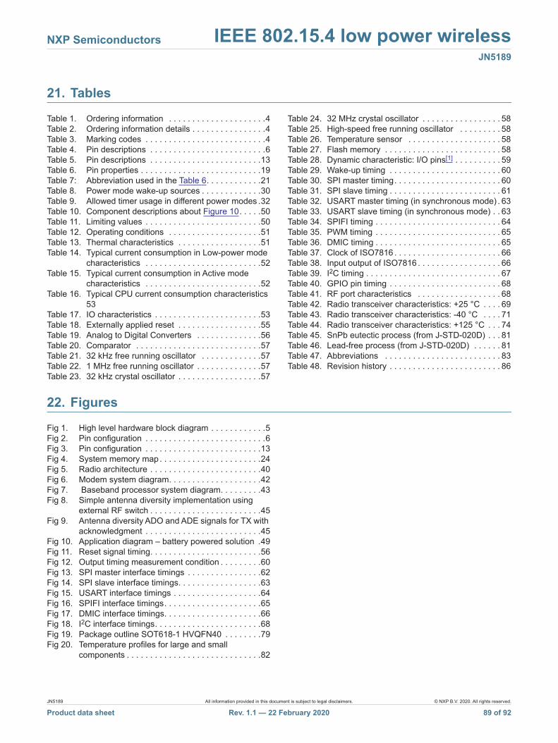
NXP Semiconductors IEEE 802.15.4 low power wirelessJN5189
21. Tables
Table 1. Ordering information . . . . . . . . . . . . . . . . . . . . .4Table 2. Ordering information details . . . . . . . . . . . . . . . .4Table 3. Marking codes . . . . . . . . . . . . . . . . . . . . . . . . . .4Table 4. Pin descriptions . . . . . . . . . . . . . . . . . . . . . . . . .6Table 5. Pin descriptions . . . . . . . . . . . . . . . . . . . . . . . .13Table 6. Pin properties . . . . . . . . . . . . . . . . . . . . . . . . . .19Table 7: Abbreviation used in the Table 6. . . . . . . . . . . .21Table 8. Power mode wake-up sources . . . . . . . . . . . . .30Table 9. Allowed timer usage in different power modes .32Table 10. Component descriptions about Figure 10. . . . .50Table 11. Limiting values . . . . . . . . . . . . . . . . . . . . . . . . .50Table 12. Operating conditions . . . . . . . . . . . . . . . . . . . .51Table 13. Thermal characteristics . . . . . . . . . . . . . . . . . .51Table 14. Typical current consumption in Low-power mode
characteristics . . . . . . . . . . . . . . . . . . . . . . . . .52Table 15. Typical current consumption in Active mode
characteristics . . . . . . . . . . . . . . . . . . . . . . . . .52Table 16. Typical CPU current consumption characteristics
53Table 17. IO characteristics . . . . . . . . . . . . . . . . . . . . . . .53Table 18. Externally applied reset . . . . . . . . . . . . . . . . . .55Table 19. Analog to Digital Converters . . . . . . . . . . . . . .56Table 20. Comparator . . . . . . . . . . . . . . . . . . . . . . . . . . .57Table 21. 32 kHz free running oscillator . . . . . . . . . . . . .57Table 22. 1 MHz free running oscillator . . . . . . . . . . . . . .57Table 23. 32 kHz crystal oscillator . . . . . . . . . . . . . . . . . .57
Table 24. 32 MHz crystal oscillator . . . . . . . . . . . . . . . . . 58Table 25. High-speed free running oscillator . . . . . . . . . 58Table 26. Temperature sensor . . . . . . . . . . . . . . . . . . . . 58Table 27. Flash memory . . . . . . . . . . . . . . . . . . . . . . . . . 58Table 28. Dynamic characteristic: I/O pins[1] . . . . . . . . . . 59Table 29. Wake-up timing . . . . . . . . . . . . . . . . . . . . . . . . 60Table 30. SPI master timing. . . . . . . . . . . . . . . . . . . . . . . 60Table 31. SPI slave timing . . . . . . . . . . . . . . . . . . . . . . . . 61Table 32. USART master timing (in synchronous mode) . 63Table 33. USART slave timing (in synchronous mode) . . 63Table 34. SPIFI timing . . . . . . . . . . . . . . . . . . . . . . . . . . . 64Table 35. PWM timing . . . . . . . . . . . . . . . . . . . . . . . . . . . 65Table 36. DMIC timing . . . . . . . . . . . . . . . . . . . . . . . . . . . 65Table 37. Clock of ISO7816 . . . . . . . . . . . . . . . . . . . . . . . 66Table 38. Input output of ISO7816 . . . . . . . . . . . . . . . . . . 66Table 39. I2C timing . . . . . . . . . . . . . . . . . . . . . . . . . . . . . 67Table 40. GPIO pin timing . . . . . . . . . . . . . . . . . . . . . . . . 68Table 41. RF port characteristics . . . . . . . . . . . . . . . . . . 68Table 42. Radio transceiver characteristics: +25 °C . . . . 69Table 43. Radio transceiver characteristics: -40 °C . . . . 71Table 44. Radio transceiver characteristics: +125 °C . . . 74Table 45. SnPb eutectic process (from J-STD-020D) . . . 81Table 46. Lead-free process (from J-STD-020D) . . . . . . 81Table 47. Abbreviations . . . . . . . . . . . . . . . . . . . . . . . . . 83Table 48. Revision history . . . . . . . . . . . . . . . . . . . . . . . . 86
22. Figures
Fig 1. High level hardware block diagram . . . . . . . . . . . .5Fig 2. Pin configuration . . . . . . . . . . . . . . . . . . . . . . . . . .6Fig 3. Pin configuration . . . . . . . . . . . . . . . . . . . . . . . . .13Fig 4. System memory map. . . . . . . . . . . . . . . . . . . . . .24Fig 5. Radio architecture . . . . . . . . . . . . . . . . . . . . . . . .40Fig 6. Modem system diagram. . . . . . . . . . . . . . . . . . . .42Fig 7. Baseband processor system diagram. . . . . . . . .43Fig 8. Simple antenna diversity implementation using
external RF switch . . . . . . . . . . . . . . . . . . . . . . . .45Fig 9. Antenna diversity ADO and ADE signals for TX with
acknowledgment . . . . . . . . . . . . . . . . . . . . . . . . .45Fig 10. Application diagram – battery powered solution .49Fig 11. Reset signal timing. . . . . . . . . . . . . . . . . . . . . . . .56Fig 12. Output timing measurement condition . . . . . . . . .60Fig 13. SPI master interface timings . . . . . . . . . . . . . . . .62Fig 14. SPI slave interface timings. . . . . . . . . . . . . . . . . .63Fig 15. USART interface timings . . . . . . . . . . . . . . . . . . .64Fig 16. SPIFI interface timings. . . . . . . . . . . . . . . . . . . . .65Fig 17. DMIC interface timings. . . . . . . . . . . . . . . . . . . . .66Fig 18. I2C interface timings. . . . . . . . . . . . . . . . . . . . . . .68Fig 19. Package outline SOT618-1 HVQFN40 . . . . . . . .79Fig 20. Temperature profiles for large and small
components . . . . . . . . . . . . . . . . . . . . . . . . . . . . .82
JN5189 All information provided in this document is subject to legal disclaimers. © NXP B.V. 2020. All rights reserved.
Product data sheet Rev. 1.1 — 22 February 2020 89 of 92
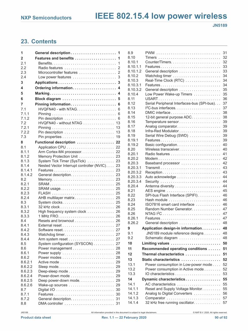
NXP Semiconductors IEEE 802.15.4 low power wirelessJN5189
23. Contents
1 General description . . . . . . . . . . . . . . . . . . . . . . 12 Features and benefits . . . . . . . . . . . . . . . . . . . . 12.1 Benefits. . . . . . . . . . . . . . . . . . . . . . . . . . . . . . . 12.2 Radio features . . . . . . . . . . . . . . . . . . . . . . . . . 22.3 Microcontroller features . . . . . . . . . . . . . . . . . . 22.4 Low power features . . . . . . . . . . . . . . . . . . . . . 33 Applications . . . . . . . . . . . . . . . . . . . . . . . . . . . . 34 Ordering information . . . . . . . . . . . . . . . . . . . . . 45 Marking . . . . . . . . . . . . . . . . . . . . . . . . . . . . . . . . 46 Block diagram . . . . . . . . . . . . . . . . . . . . . . . . . . 57 Pinning information . . . . . . . . . . . . . . . . . . . . . . 67.1 HVQFN40 - with NTAG. . . . . . . . . . . . . . . . . . . 67.1.1 Pinning . . . . . . . . . . . . . . . . . . . . . . . . . . . . . . . 67.1.2 Pin description . . . . . . . . . . . . . . . . . . . . . . . . . 67.2 HVQFN40 - without NTAG . . . . . . . . . . . . . . . 137.2.1 Pinning . . . . . . . . . . . . . . . . . . . . . . . . . . . . . . 137.2.2 Pin description . . . . . . . . . . . . . . . . . . . . . . . . 137.3 Pin properties . . . . . . . . . . . . . . . . . . . . . . . . . 198 Functional description . . . . . . . . . . . . . . . . . . 228.1 Application CPU . . . . . . . . . . . . . . . . . . . . . . . 228.1.1 Arm Cortex-M4 processor. . . . . . . . . . . . . . . . 228.1.2 Memory Protection Unit . . . . . . . . . . . . . . . . . 238.1.3 System Tick Timer (SysTick) . . . . . . . . . . . . . 238.1.4 Nested Vector Interrupt controller (NVIC) . . . . 238.1.4.1 Features . . . . . . . . . . . . . . . . . . . . . . . . . . . . . 238.1.4.2 General description. . . . . . . . . . . . . . . . . . . . . 238.2 Memory. . . . . . . . . . . . . . . . . . . . . . . . . . . . . . 238.2.1 SRAM . . . . . . . . . . . . . . . . . . . . . . . . . . . . . . . 258.2.2 SRAM usage. . . . . . . . . . . . . . . . . . . . . . . . . . 258.2.3 FLASH . . . . . . . . . . . . . . . . . . . . . . . . . . . . . . 258.2.4 AHB multilayer matrix . . . . . . . . . . . . . . . . . . . 258.3 System clocks. . . . . . . . . . . . . . . . . . . . . . . . . 258.3.1 32 kHz clock . . . . . . . . . . . . . . . . . . . . . . . . . . 268.3.2 High frequency system clock . . . . . . . . . . . . . 268.3.3 1 MHz FRO. . . . . . . . . . . . . . . . . . . . . . . . . . . 268.4 Resets and brownout . . . . . . . . . . . . . . . . . . . 268.4.1 External reset . . . . . . . . . . . . . . . . . . . . . . . . . 278.4.2 Software reset. . . . . . . . . . . . . . . . . . . . . . . . . 278.4.3 Watchdog timer. . . . . . . . . . . . . . . . . . . . . . . . 278.4.4 Arm system reset . . . . . . . . . . . . . . . . . . . . . . 278.5 System configuration (SYSCON) . . . . . . . . . . 278.6 Power management . . . . . . . . . . . . . . . . . . . . 288.6.1 Power supply . . . . . . . . . . . . . . . . . . . . . . . . . 288.6.2 Power modes . . . . . . . . . . . . . . . . . . . . . . . . . 288.6.2.1 Active mode . . . . . . . . . . . . . . . . . . . . . . . . . . 298.6.2.2 Sleep mode. . . . . . . . . . . . . . . . . . . . . . . . . . . 298.6.2.3 Deep-sleep mode . . . . . . . . . . . . . . . . . . . . . . 298.6.2.4 Power-down mode . . . . . . . . . . . . . . . . . . . . . 298.6.2.5 Deep power-down mode. . . . . . . . . . . . . . . . . 298.6.2.6 Wake-up sources . . . . . . . . . . . . . . . . . . . . . . 298.7 Digital I/O . . . . . . . . . . . . . . . . . . . . . . . . . . . . 308.7.1 Features . . . . . . . . . . . . . . . . . . . . . . . . . . . . . 308.7.2 General description. . . . . . . . . . . . . . . . . . . . . 318.8 DMA controller . . . . . . . . . . . . . . . . . . . . . . . . 31
8.9 PWM . . . . . . . . . . . . . . . . . . . . . . . . . . . . . . . 318.10 Timers . . . . . . . . . . . . . . . . . . . . . . . . . . . . . . 328.10.1 Counter/Timers. . . . . . . . . . . . . . . . . . . . . . . . 328.10.1.1 Features . . . . . . . . . . . . . . . . . . . . . . . . . . . . . 338.10.1.2 General description . . . . . . . . . . . . . . . . . . . . 338.10.2 Watchdog timer . . . . . . . . . . . . . . . . . . . . . . . 348.10.3 Real-Time Clock (RTC) . . . . . . . . . . . . . . . . . 348.10.3.1 Features . . . . . . . . . . . . . . . . . . . . . . . . . . . . . 348.10.3.2 General description . . . . . . . . . . . . . . . . . . . . 358.10.4 Low Power Wake-up Timers . . . . . . . . . . . . . 358.11 USART . . . . . . . . . . . . . . . . . . . . . . . . . . . . . . 368.12 Serial Peripheral Interfaces-bus (SPI-bus). . . 378.13 I2C-bus interfaces. . . . . . . . . . . . . . . . . . . . . . 378.14 DMIC interface . . . . . . . . . . . . . . . . . . . . . . . . 388.15 12-bit general purpose ADC. . . . . . . . . . . . . . 388.16 Temperature sensor . . . . . . . . . . . . . . . . . . . . 398.17 Analog comparator. . . . . . . . . . . . . . . . . . . . . 398.18 Infra-Red Modulator . . . . . . . . . . . . . . . . . . . . 398.19 Serial Wire Debug (SWD) . . . . . . . . . . . . . . . 398.19.1 Features . . . . . . . . . . . . . . . . . . . . . . . . . . . . . 398.19.2 Basic configuration. . . . . . . . . . . . . . . . . . . . . 408.20 Wireless transceiver. . . . . . . . . . . . . . . . . . . . 408.20.1 Radio features . . . . . . . . . . . . . . . . . . . . . . . . 418.20.2 Modem . . . . . . . . . . . . . . . . . . . . . . . . . . . . . . 428.20.3 Baseband processor . . . . . . . . . . . . . . . . . . . 428.20.3.1 Transmit . . . . . . . . . . . . . . . . . . . . . . . . . . . . . 438.20.3.2 Reception . . . . . . . . . . . . . . . . . . . . . . . . . . . . 438.20.3.3 Auto acknowledge . . . . . . . . . . . . . . . . . . . . . 448.20.3.4 Security . . . . . . . . . . . . . . . . . . . . . . . . . . . . . 448.20.4 Antenna diversity . . . . . . . . . . . . . . . . . . . . . . 448.21 AES engine . . . . . . . . . . . . . . . . . . . . . . . . . . 458.22 SPI-bus Flash Interface (SPIFI) . . . . . . . . . . . 468.23 Hash module . . . . . . . . . . . . . . . . . . . . . . . . . 468.24 ISO7816 smart card interface . . . . . . . . . . . . 468.25 Random Number Generator. . . . . . . . . . . . . . 478.26 NTAG I2C . . . . . . . . . . . . . . . . . . . . . . . . . . . . 478.26.1 Features . . . . . . . . . . . . . . . . . . . . . . . . . . . . . 478.26.2 General description . . . . . . . . . . . . . . . . . . . . 489 Application design-in information . . . . . . . . . 489.1 JN5189 module reference designs . . . . . . . . 489.2 Schematic diagram . . . . . . . . . . . . . . . . . . . . 4810 Limiting values . . . . . . . . . . . . . . . . . . . . . . . . 5011 Recommended operating conditions . . . . . . 5112 Thermal characteristics . . . . . . . . . . . . . . . . . 5113 Static characteristics . . . . . . . . . . . . . . . . . . . 5213.1 Power consumption in Low-power mode . . . . 5213.2 Power consumption in Active mode . . . . . . . . 5213.3 IO characteristics . . . . . . . . . . . . . . . . . . . . . . 5314 Dynamic characteristics . . . . . . . . . . . . . . . . . 5514.1 AC characteristics . . . . . . . . . . . . . . . . . . . . . 5514.1.1 Reset and Supply Voltage Monitor. . . . . . . . . 5514.1.2 Analog to Digital Converters . . . . . . . . . . . . . 5614.1.3 Comparator . . . . . . . . . . . . . . . . . . . . . . . . . . 5714.1.4 32 kHz free running oscillator. . . . . . . . . . . . . 57
JN5189 All information provided in this document is subject to legal disclaimers. © NXP B.V. 2020. All rights reserved.
Product data sheet Rev. 1.1 — 22 February 2020 90 of 92
NXP Semiconductors IEEE 802.15.4 low power wirelessJN5189
14.1.5 1 MHz free running oscillator . . . . . . . . . . . . . 5714.1.6 32 kHz crystal oscillator . . . . . . . . . . . . . . . . . 5714.1.7 32 MHz crystal oscillator. . . . . . . . . . . . . . . . . 5814.1.8 High-speed free running oscillator . . . . . . . . . 5814.1.9 Temperature sensor . . . . . . . . . . . . . . . . . . . . 5814.2 Flash memory . . . . . . . . . . . . . . . . . . . . . . . . . 5814.3 IO pins . . . . . . . . . . . . . . . . . . . . . . . . . . . . . . 5914.4 Wake-up timing. . . . . . . . . . . . . . . . . . . . . . . . 6014.5 SPI timing . . . . . . . . . . . . . . . . . . . . . . . . . . . . 6014.6 USART timing . . . . . . . . . . . . . . . . . . . . . . . . . 6314.7 SPIFI timing . . . . . . . . . . . . . . . . . . . . . . . . . . 6414.8 PWM timing . . . . . . . . . . . . . . . . . . . . . . . . . . 6514.9 DMIC timing . . . . . . . . . . . . . . . . . . . . . . . . . . 6514.10 ISO7816 . . . . . . . . . . . . . . . . . . . . . . . . . . . . . 6614.11 I2C timing . . . . . . . . . . . . . . . . . . . . . . . . . . . . 6714.12 GPIO pin timing . . . . . . . . . . . . . . . . . . . . . . . 6814.13 Radio transceiver . . . . . . . . . . . . . . . . . . . . . . 6815 Package outline . . . . . . . . . . . . . . . . . . . . . . . . 7916 Soldering of SMD packages . . . . . . . . . . . . . . 8016.1 Introduction to soldering . . . . . . . . . . . . . . . . . 8016.2 Wave and reflow soldering . . . . . . . . . . . . . . . 8016.3 Wave soldering . . . . . . . . . . . . . . . . . . . . . . . . 8016.4 Reflow soldering . . . . . . . . . . . . . . . . . . . . . . . 8117 Abbreviations. . . . . . . . . . . . . . . . . . . . . . . . . . 8318 References . . . . . . . . . . . . . . . . . . . . . . . . . . . . 8519 Revision history . . . . . . . . . . . . . . . . . . . . . . . . 8620 Legal information. . . . . . . . . . . . . . . . . . . . . . . 8720.1 Data sheet status . . . . . . . . . . . . . . . . . . . . . . 8720.2 Definitions . . . . . . . . . . . . . . . . . . . . . . . . . . . . 8720.3 Disclaimers . . . . . . . . . . . . . . . . . . . . . . . . . . . 8720.4 Trademarks. . . . . . . . . . . . . . . . . . . . . . . . . . . 8821 Contact information. . . . . . . . . . . . . . . . . . . . . 8822 Tables . . . . . . . . . . . . . . . . . . . . . . . . . . . . . . . . 8923 Figures . . . . . . . . . . . . . . . . . . . . . . . . . . . . . . . 8924 Contents . . . . . . . . . . . . . . . . . . . . . . . . . . . . . . 90
JN5189 All information provided in this document is subject to legal disclaimers. © NXP B.V. 2020. All rights reserved.
Product data sheet Rev. 1.1 — 22 February 2020 91 of 92
Information in this document is provided solely to enable system and software implementers to use
NXP products. There are no express or implied copyright licenses granted hereunder to design or
fabricate any integrated circuits based on the information in this document. NXP reserves the right to
make changes without further notice to any products herein.
NXP makes no warranty, representation, or guarantee regarding the suitability of its products for any
particular purpose, nor does NXP assume any liability arising out of the application or use of any
product or circuit, and specifically disclaims any and all liability, including without limitation
consequential or incidental damages. “Typical” parameters that may be provided in NXP data sheets
and/or specifications can and do vary in different applications, and actual performance may vary over
time. All operating parameters, including “typicals” must be validated for each customer application
by customer‚ customer’s technical experts. NXP does not convey any license under its patent rights
nor the rights of others. NXP sells products pursuant to standard terms and conditions of sale, which
can be found at the following address: nxp.com/SalesTermsandConditions.
How to Reach Us:
Home Page: nxp.com
Web Support: nxp.com/support
While NXP has implemented advanced security features, all products may be subject to unidentified
vulnerabilities. Customers are responsible for the design and operation of their applications and
products to reduce the effect of these vulnerabilities on customer’s applications and products, and
NXP accepts no liability for any vulnerability that is discovered. Customers should implement
appropriate design and operating safeguards to minimize the risks associated with their applications
and products.
NXP, the NXP logo, NXP SECURE CONNECTIONS FOR A SMARTER WORLD, COOLFLUX,
EMBRACE, GREENCHIP, HITAG, I2C BUS, ICODE, JCOP, LIFE VIBES, MIFARE, MIFARE
CLASSIC, MIFARE DESFire, MIFARE PLUS, MIFARE FLEX, MANTIS, MIFARE ULTRALIGHT,
MIFARE4MOBILE, MIGLO, NTAG, ROADLINK, SMARTLX, SMARTMX, STARPLUG, TOPFET,
TRENCHMOS, UCODE, Freescale, the Freescale logo, AltiVec, C-5, CodeTEST, CodeWarrior,
ColdFire, ColdFire+, C-Ware, the Energy Efficient Solutions logo, Kinetis, Layerscape, MagniV,
mobileGT, PEG, PowerQUICC, Processor Expert, QorIQ, QorIQ Qonverge, Ready Play,
SafeAssure, the SafeAssure logo, StarCore, Symphony, VortiQa, Vybrid, Airfast, BeeKit, BeeStack,
CoreNet, Flexis, MXC, Platform in a Package, QUICC Engine, SMARTMOS, Tower, TurboLink,
UMEMS, EdgeScale, EdgeLock, eIQ, and Immersive3D are trademarks of NXP B.V. All other product
or service names are the property of their respective owners. AMBA, Arm, Arm7, Arm7TDMI, Arm9,
Arm11, Artisan, big.LITTLE, Cordio, CoreLink, CoreSight, Cortex, DesignStart, DynamIQ, Jazelle,
Keil, Mali, Mbed, Mbed Enabled, NEON, POP, RealView, SecurCore, Socrates, Thumb, TrustZone,
ULINK, ULINK2, ULINK-ME, ULINK-PLUS, ULINKpro, μVision, Versatile are trademarks or
registered trademarks of Arm Limited (or its subsidiaries) in the US and/or elsewhere. The related
technology may be protected by any or all of patents, copyrights, designs and trade secrets. All rights
reserved. Oracle and Java are registered trademarks of Oracle and/or its affiliates. The Power
Architecture and Power.org word marks and the Power and Power.org logos and related marks are
trademarks and service marks licensed by Power.org.
© 2020 NXP B.V.Document Number: JN5189
Rev. 1.102/2020