JESD204B Overview - Analog, Embedded Processing, … · · 2016-07-26JESD204B Overview Texas...
32
JESD204B Overview Texas Instruments High Speed Data Converter Training
-
Upload
duongtuyen -
Category
Documents
-
view
219 -
download
3
Transcript of JESD204B Overview - Analog, Embedded Processing, … · · 2016-07-26JESD204B Overview Texas...

JESD204B Overview Texas Instruments High Speed Data Converter Training

Outline
• JESD204B Standard at a Glance
• Benefits / Cost
• Timing Signals
• Layers Overview (Transport, Link, Physical)
• Deterministic Latency
• Subclasses

JESD204B Standard at a Glance
• A standardized serial interface between data converters (ADCs and
DACs) and logic devices (FPGAs or ASICs)
• Serial data rates up to 12.5 Gbps
• Mechanism to achieve deterministic latency across the serial link
• Uses 8b/10b encoding for SerDes synchronization, clock recovery and
DC balance
• JESD204B is a must for high density systems!

TI Information – NDA Required
Feature JESD204 JESD204A JESD204B
Introduction of Standard 2006 2008 2011
Maximum Lane Rate 3.125 Gbps 3.125 Gbps 12.5 Gbps
Multiple Lane Support No Yes Yes
Multi-Lane Synchronization No Yes Yes
Multi-Device Synchronization No Yes Yes
Deterministic Latency No No Yes
Harmonic Clocking No No Yes
JESD204B Standard at a Glance
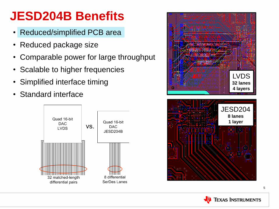
JESD204B Benefits
5
• Reduced/simplified PCB area
• Reduced package size
• Comparable power for large throughput
• Scalable to higher frequencies
• Simplified interface timing
• Standard interface
DAC
LVDS 32 lanes
4 layers
JESD204 8 lanes
1 layer

JESD204B Benefits
6
DAC
DAC
10x10mm
144-pin BGA
DAC
12x12mm
196-pin BGA
• Reduced/simplified PCB area
• Reduced package size
• Comparable power for large throughput
• Scalable to higher frequencies
• Simplified interface timing
• Standard interface

JESD204B Benefits
7
• Reduced/simplified PCB area
• Reduced package size
• Comparable power for large throughput
• Scalable to higher frequencies
• Simplified interface timing
• Standard interface
3.5mA
LVDS Driver
16mA
CML Driver
PLL
@ 1.25GB/s
x32
@ 10GB/s
x450mA

JESD204B Benefits
8
Data
Clock
D Q
Data D Q
CDR
Refclk
Speed limited by setup/hold
due to PVT variation
Speed scalable using
SERDES/CDR techniques
LVDS Rx
SERDES Rx
Data
Clock
Data
CDR
• Reduced/simplified PCB area
• Reduced package size
• Comparable power for large throughput
• Scalable to higher frequencies
• Simplified interface timing
• Standard interface

JESD204B Benefits
• Reduced/simplified PCB area
• Reduced package size
• Comparable power for large throughput
• Scalable to higher frequencies
• Simplified interface timing
• Standard interface
9
D0
Clock
...
D1
D2
DN
LVDS Timing
D0
CDR0
D1
CDR1
SERDES Timing

JESD204B Benefits
• Reduced/simplified PCB area
• Reduced package size
• Comparable power for large throughput
• Scalable to higher frequencies
• Simplified interface timing
• Standard interface
10
11
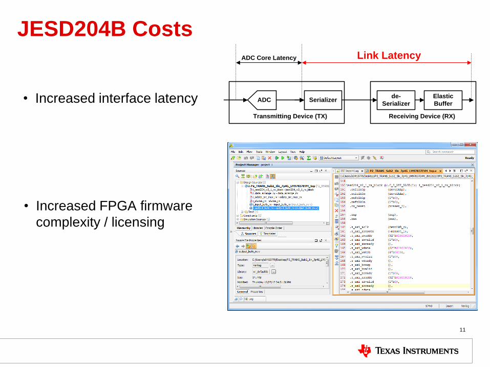
JESD204B Costs
ADC Serializerde-
Serializer
Elastic
Buffer
Transmitting Device (TX) Receiving Device (RX)
Link LatencyADC Core Latency
• Increased interface latency
• Increased FPGA firmware
complexity / licensing
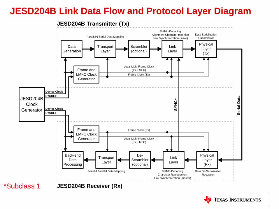
JESD204B Link Data Flow and Protocol Layer Diagram
JESD204B
Clock
Generator
Frame and
LMFC Clock
Generator
Data
Generation
Transport
Layer
ParallelàSerial Data Mapping
Scrambler
(optional)
Link
Layer
8b/10b Encoding
Alignment Character Insertion
Link Synchronization (slave)
Physical
Layer
(Tx)
Data Serialization
Transmission
Frame Clock (Tx)
Local Multi-Frame Clock
(Tx, LMFC)
JESD204B Transmitter (Tx)
Device Clock
SYSREF
Device Clock
SYSREF
Back-end
Data
Processing
Transport
Layer
SerialàParallel Data Mapping
De-
Scrambler
(optional)
Link
Layer
8b/10b Decoding
Character Replacement
Link Synchronization (master)
Physical
Layer
(Rx)
Data De-Serialization
Reception
Frame and
LMFC Clock
Generator
SY
NC
~
Frame Clock (Rx)
Local Multi-Frame Clock
(Rx, LMFC)
JESD204B Receiver (Rx)
Se
ria
l D
ata
*Subclass 1

JESD204 Timing Signals/Terminology
TI Information – NDA Required
Frame Clock
• Data frame of the transport layer is aligned to the frame clock
• Frame clock period in all the TX and RX devices must be identical
Local Multi-Frame Clock (LMFC)
• Multi-Frame is composed of ‘K’ Frames
• LMFC is aligned to the multi-frame boundary
• Acts as a low-frequency reference to resolve frame clock phase
ambiguity across multiple devices
• LMFC period in all TX and RX devices must be identical

JESD204 Timing Signals/Terminology
TI Information – NDA Required
Device Clock
• System clock from which the device’s frame, sampling, LMFC clocks
are derived (externally applied)
Sample Clock
• Internal conversion clock of data converter
• Derived from Device Clock (via multipliers or dividers)
• Relationship to frame clock depends on packing of data into frame
SYSREF
• Timing phase reference from which LMFC clocks are generated in
subclass 1 implementations (externally applied)
• Must be source synchronous with Device Clock
• Rising edge transition determines LMFC alignment

JESD204 Timing Signals/Terminology
TI Information – NDA Required
SYNC
• Unidirectional, Receiver-to-Transmitter
• Active low signaling, often referred to as ‘SYNC~’ or ‘SYNCb’
• Mainly used for device synchronization requests and error reporting
• Aligns LMFC phase in Subclass 2 devices
• Options available for distributing SYNC to multiple devices

Transport Layer Overview
• Maps the data à octets à frames consisting of multiple octets
• Adds optional control bits to samples if needed
• Distinguishes the possible combinations of device/links/lanes/etc.
• Important parameters associated with transport layer include:
– L # of lanes per converter device
– M # of converters per device
– F # of octets per frame (per lane)
– S # of samples per converter per frame clock cycle
– CS # of control bits per conversion sample
TI Information – NDA Required

N+1 N
Tra
ns
po
rt L
ay
er
11-bit Samples
...
10
9
1
0
N-1
N+1 N
...
10
9
1
0
...
10
9
1
0
N-1
...
10
9
1
0
N+1 N
...
10
9
1
0
...
10
9
1
0
N-1
...
10
9
1
0
N+1 N
...
10
9
1
0
...
10
9
1
0
N-1
...
10
9
1
0
...
10
9
1
0
...
10
9
1
0
Core 7 [10:3] Core 7 [2:0] T TTC1 C0Core 6 [10:3] Core 6 [2:0] T TTC1 C0
Core 3 [10:3] Core 3 [2:0] T TTC1 C0Core 2 [10:3] Core 2 [2:0] T TTC1 C0
Core 5 [10:3] Core 5 [2:0] T TTC1 C0Core 4 [10:3] Core 4 [2:0] T TTC1 C0
Core 1 [10:3] Core 1 [2:0] T TTC1 C0Core 0 [10:3] Core 0 [2:0] T TTC1 C0
Transport Layer (Generic Example)
TI Information – NDA Required
Octet 3Octet 0 Octet 1 Octet 2F=4
Octets per Frame
(per lane)
M=8Converters per
Device
S=1Samples per Frame
(per converter)
N=11Converter Resolution
CS=2Control bits per
sample
N’=13Number of bits in Sample
plus control bitsTails Bits
RBD=User DefinedRelease Buffer Delay
K=User DefinedFrames per Multi-Frame
1 Frame
L=4Lanes per
Device
Lane 0
Lane 1
Lane 2
Lane 3
ADC
Core 0
ADC
Core 1
ADC
Core 6
ADC
Core 7
ADC
Cores
2-5
Mapping Converter Samples to Frames
De
vic
e

TI Information – NDA Required
Transport Layer (ex. ADS42JB49)
LMFS
2221
LMFS
4211
Note: Actual ADS42JB49 implementation defines N’=16 and inserts 0’s into LSBs instead of defining tail bits
N+1 N
Tra
ns
po
rt L
ay
er
14-bit Samples
...
13
12
1
0
N-1
N+1 N
...
13
10
1
0
...
13
10
1
0
N-1
...
13
10
1
0
...
13
12
1
0
...
13
12
1
0
M=2 S=1
N=14
Core 0 [13:6]
Core 0 [5:0] T T
Core 1 [13:6]
Core 1 [5:0] T T
Octet 0F=1
CS=0N’=14
L=4
Lane 0
Lane 1
Lane 2
Lane 3
ADC
Core 0
ADC
Core 1
De
vic
e
N+1 N
Tra
ns
po
rt L
ay
er
14-bit Samples
...
13
12
1
0
N-1
N+1 N
...
13
10
1
0
...
13
10
1
0
N-1
...
13
10
1
0
...
13
12
1
0
...
13
12
1
0
M=2 S=1
N=14
Core 0 [13:6] Core 0 [5:0] T T
Core 1 [13:6] Core 1 [5:0] T T
Octet 0 Octet 1
F=2
CS=0N’=14Tails Bits
Lane 0
Lane 1
ADC
Core 0
ADC
Core 1D
ev
ice
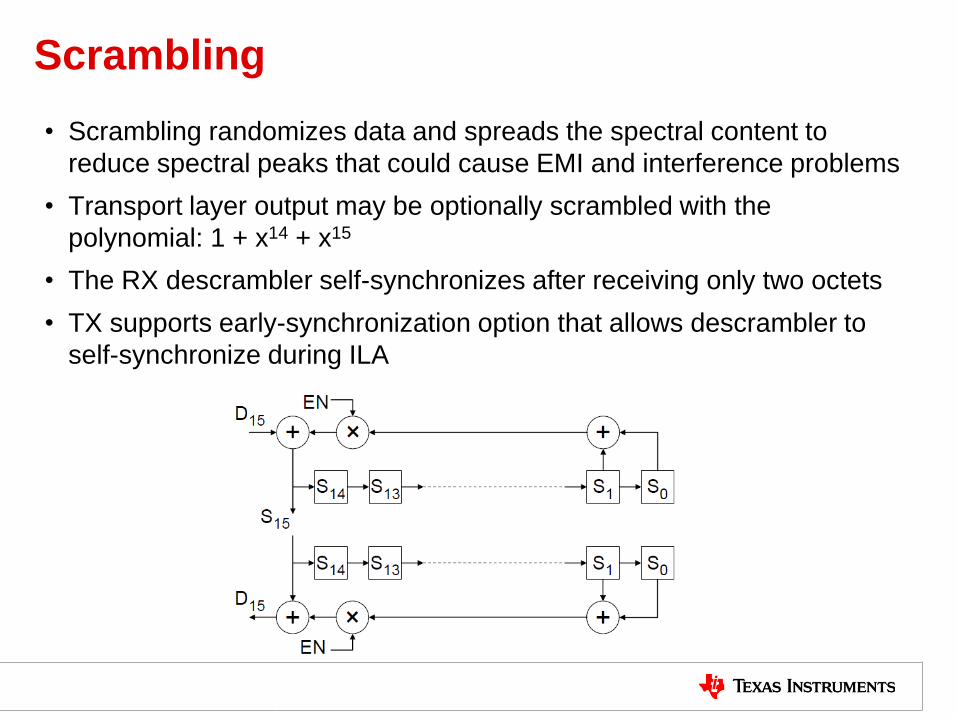
Scrambling
• Scrambling randomizes data and spreads the spectral content to
reduce spectral peaks that could cause EMI and interference problems
• Transport layer output may be optionally scrambled with the
polynomial: 1 + x14 + x15
• The RX descrambler self-synchronizes after receiving only two octets
• TX supports early-synchronization option that allows descrambler to
self-synchronize during ILA
TI Information – NDA Required

Data Link Layer
• 8b/10b Encoding
• Link Establishment, including frame and lane alignment
• Link Monitoring using control symbols
TI Information – NDA Required

Data Link Layer: 8b/10b Encoding
• Encodes 8-bit “octets” into 10-bit symbols
• Octet to symbol mapping depends on running disparity (RD)
• Coding provides many bit-transitions to enable CDR techniques
• DC balancing enables AC coupling
TI Information – NDA Required

Data Link Layer: Link Establishment
• Link Establishment accomplishes TX and RX synchronization
– Code Group Synchronization (CGS)
– Initial Frame Synchronization
– Initial Lane Synchronization
TI Information – NDA Required
SYNCb
K28.5Serial Data ILA
CLKIN
SYSREF
Tx Frame Clk
K28.5XXX
Tx LMFC Boundary
tS-SYNCb-F
SYNCb de-assertion
latched
SYNCb assertion
latched
XXX
One-shot
ILA Valid Data
SYSREF assertion
latched
Frame Clock
Alignment
Code Group
Synchronization
Initial Frame and Lane
Synchronization
Data
Transmission
tS-SYNCb-F
tS-SYStH-SYS
tD-LMFC
tH-SYNCb-F
tILA
tD-ILA
tS-SYNCb
tD-K28 tD-DATA

Physical Layer: Serial Lanes
• Physical layer defines the electrical and timing characteristics of data
transfer
• Point-to-point, unidirectional serial interface
• AC or DC compliance
• 3 signal speed-grade variants
• Performance limited by SERDES, CDR and driver/receiver blocks
Parameter LV-OIF-Sx15 LV-OIF-6G-SR LV-OIF-11G-SR
Data Rates 312.5Mbps –
3.125Gbps
312.5Mbps -
6.375Gbps
312.5Mbps – 12.5Gbps
Differential Output
Voltage
500 – 1000 (mV) 400 – 750 (mV) 360 – 770 (mV)
Bit Error Rate (BER) ≤ 1e-12
≤ 1e-15
≤ 1e-15

Deterministic Latency: Motivation
• Applications are often sensitive to the variation of system latency
– Synchronous sampling
– Multi-channel phase array alignment
– Gain control loop stability
• JESD204 and JESD204A do not achieve known/constant latency
across the link across temp/supply/reboot variation
• Providing support for devices with internal clock dividers introduces
potential for even more latency uncertainty
Deterministic Latency: Achieved
• JESD204B achieves deterministic latency: known/constant latency
– Subclass 0: DL not achieved
– Subclass 1: DL achieved using SYSREF with strict timing
– Subclass 2: DL achieved using SYNC~ with strict timing
• Deterministic Latency achieved with these architecture features
– SYSREF or SYNC~ are used to provide a deterministic reference phase to
all devices for synchronization
– LMFC provides a low frequency reference to avoid frame clock phase
ambiguity in the presence of link delay changes
– RX has an “elastic buffer” that absorbs link delay variation
• Texas Instruments recommends/supports subclass 1
– LMFC phase easier to control with source synchronous SYSREF than with
system synchronous SYNC~

TI Information – NDA Required
• Subclass distinction: Whether to, and how to achieve time reference alignment
(as a requirement for deterministic link latency)
Subclass 0 Subclass 1 Subclass 2
Deterministic
Latency
Supported?
No Yes Yes
How to achieve
Deterministic
Latency?
N/A Time reference
(LMFC) alignment
using SYSREF
Time reference
(LMFC) alignment
using ~SYNC
ADC Serializerde-
Serializer
Elastic
Buffer
Transmitting Device (TX) Receiving Device (RX)
Link LatencyADC Core Latency
JESD204B Subclasses

TI Information – NDA Required
Serial Data
SYNC~D
evic
e c
lock
Transmitter
JESD204B
Subclass 0
Receiver
JESD204B
Subclass 0
Clock
Generator
De
vic
e c
lock
SUBCLASS 0
Serial Data
SYNC~
De
vic
e c
lock
Transmitter
JESD204B
Subclass 1
Receiver
JESD204B
Subclass 1
JESD204B
Clock
Generator
SY
SR
EF Device Clock
SYSREF
De
vic
e c
lock
SY
SR
EF
SUBCLASS 1
Serial Data
SYNC~
De
vic
e c
lock
Transmitter
JESD204B
Subclass 2
Receiver
JESD204B
Subclass 2
Clock
Generator
Device Clock
~SYNC
De
vic
e c
lock
SUBCLASS 2
Subclass Signaling Requirements

TI Information – NDA Required
Subclass 0 Subclass 1 Subclass 2
JESD204A
Backward Compatible?
Yes No No
Deterministic Latency
Supported?
No Yes Yes, but speed
limited
SYSREF Required? No Yes No
Clock and Sync Signals Device Clock
SYNC~
Device Clock
SYSREF
SYNC~
Device Clock
SYNC~
SYNC~ is Timing Critical? No No Yes
Interface Hardware
Complexity
Least Most Moderate
Link Latency 8-100 sample clocks (non-deterministic)
15-120 sample clocks (deterministic)
Choosing a Subclass

TI Information – NDA Required
Subclass 0 Subclass 1 Subclass 2
Wireless Comms. Repeater
- Narrowband (<125 MSPS ADC)
- No DL requirements
Software Defined Radio
- Wideband
- DL required
Radar, Imaging Sensor
- Wideband (>250 MSPS ADC)
- DL required + Multi-Device Sync.
Oscilloscope, Spectrum Analyzer
- Wideband (> 250 MSPS ADC) No DL Required DL Required
• Texas Instruments’ JESD204B device all support subclass 1 while some support
all 3 subclasses
>250 MSPS ADC <=250 MSPS ADC
Subclass by Application Examples

Summary
• JESD204: Standard serial data interface for data converters
• JESD204B subclasses offer 3 implementation variations
• Transport Layer defines data framing into serial lanes
• Link layer defines encoding, synchronization and data monitoring
• Physical layer defines the electrical and timing performance
• Deterministic latency achieved with subclasses 1, 2 and is required for
known/constant latency through link
TI Information – NDA Required

www.ti.com/lsds/ti/data-converters/high-speed-adc-greater-10msps-jesd204b.page
More Educational Resources

IMPORTANT NOTICE
Texas Instruments Incorporated and its subsidiaries (TI) reserve the right to make corrections, enhancements, improvements and otherchanges to its semiconductor products and services per JESD46, latest issue, and to discontinue any product or service per JESD48, latestissue. Buyers should obtain the latest relevant information before placing orders and should verify that such information is current andcomplete. All semiconductor products (also referred to herein as “components”) are sold subject to TI’s terms and conditions of salesupplied at the time of order acknowledgment.TI warrants performance of its components to the specifications applicable at the time of sale, in accordance with the warranty in TI’s termsand conditions of sale of semiconductor products. Testing and other quality control techniques are used to the extent TI deems necessaryto support this warranty. Except where mandated by applicable law, testing of all parameters of each component is not necessarilyperformed.TI assumes no liability for applications assistance or the design of Buyers’ products. Buyers are responsible for their products andapplications using TI components. To minimize the risks associated with Buyers’ products and applications, Buyers should provideadequate design and operating safeguards.TI does not warrant or represent that any license, either express or implied, is granted under any patent right, copyright, mask work right, orother intellectual property right relating to any combination, machine, or process in which TI components or services are used. Informationpublished by TI regarding third-party products or services does not constitute a license to use such products or services or a warranty orendorsement thereof. Use of such information may require a license from a third party under the patents or other intellectual property of thethird party, or a license from TI under the patents or other intellectual property of TI.Reproduction of significant portions of TI information in TI data books or data sheets is permissible only if reproduction is without alterationand is accompanied by all associated warranties, conditions, limitations, and notices. TI is not responsible or liable for such altereddocumentation. Information of third parties may be subject to additional restrictions.Resale of TI components or services with statements different from or beyond the parameters stated by TI for that component or servicevoids all express and any implied warranties for the associated TI component or service and is an unfair and deceptive business practice.TI is not responsible or liable for any such statements.Buyer acknowledges and agrees that it is solely responsible for compliance with all legal, regulatory and safety-related requirementsconcerning its products, and any use of TI components in its applications, notwithstanding any applications-related information or supportthat may be provided by TI. Buyer represents and agrees that it has all the necessary expertise to create and implement safeguards whichanticipate dangerous consequences of failures, monitor failures and their consequences, lessen the likelihood of failures that might causeharm and take appropriate remedial actions. Buyer will fully indemnify TI and its representatives against any damages arising out of the useof any TI components in safety-critical applications.In some cases, TI components may be promoted specifically to facilitate safety-related applications. With such components, TI’s goal is tohelp enable customers to design and create their own end-product solutions that meet applicable functional safety standards andrequirements. Nonetheless, such components are subject to these terms.No TI components are authorized for use in FDA Class III (or similar life-critical medical equipment) unless authorized officers of the partieshave executed a special agreement specifically governing such use.Only those TI components which TI has specifically designated as military grade or “enhanced plastic” are designed and intended for use inmilitary/aerospace applications or environments. Buyer acknowledges and agrees that any military or aerospace use of TI componentswhich have not been so designated is solely at the Buyer's risk, and that Buyer is solely responsible for compliance with all legal andregulatory requirements in connection with such use.TI has specifically designated certain components as meeting ISO/TS16949 requirements, mainly for automotive use. In any case of use ofnon-designated products, TI will not be responsible for any failure to meet ISO/TS16949.
Products ApplicationsAudio www.ti.com/audio Automotive and Transportation www.ti.com/automotiveAmplifiers amplifier.ti.com Communications and Telecom www.ti.com/communicationsData Converters dataconverter.ti.com Computers and Peripherals www.ti.com/computersDLP® Products www.dlp.com Consumer Electronics www.ti.com/consumer-appsDSP dsp.ti.com Energy and Lighting www.ti.com/energyClocks and Timers www.ti.com/clocks Industrial www.ti.com/industrialInterface interface.ti.com Medical www.ti.com/medicalLogic logic.ti.com Security www.ti.com/securityPower Mgmt power.ti.com Space, Avionics and Defense www.ti.com/space-avionics-defenseMicrocontrollers microcontroller.ti.com Video and Imaging www.ti.com/videoRFID www.ti-rfid.comOMAP Applications Processors www.ti.com/omap TI E2E Community e2e.ti.comWireless Connectivity www.ti.com/wirelessconnectivity
Mailing Address: Texas Instruments, Post Office Box 655303, Dallas, Texas 75265Copyright © 2016, Texas Instruments Incorporated