JEDEC Strategic Roadmap All Committee... · JEDEC Strategic Roadmap Strategic Planning Task Group...
20
JEDEC Strategic Roadmap Strategic Planning Task Group JEDEC Board of Directors Perry Keller, Keysight Technologies – TG Chairman JEDEC All-Member Update June 8, 2016
Transcript of JEDEC Strategic Roadmap All Committee... · JEDEC Strategic Roadmap Strategic Planning Task Group...

JEDEC Strategic Roadmap
Strategic Planning Task Group JEDEC Board of Directors
Perry Keller, Keysight Technologies – TG Chairman
JEDEC All-Member Update June 8, 2016
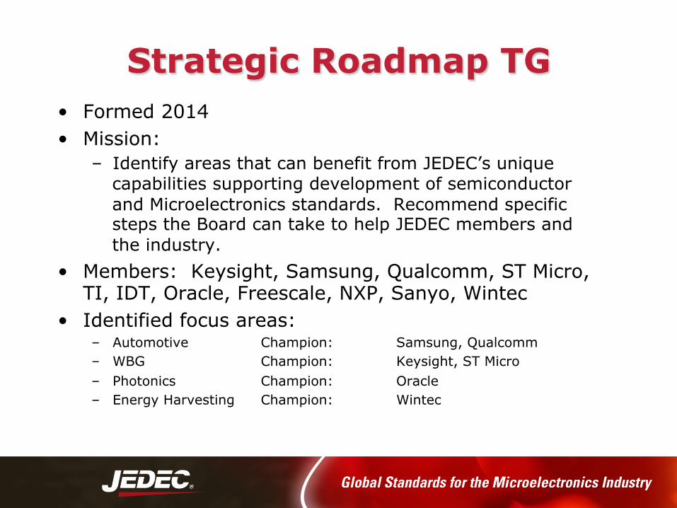
Strategic Roadmap TG • Formed 2014 • Mission:
– Identify areas that can benefit from JEDEC’s unique capabilities supporting development of semiconductor and Microelectronics standards. Recommend specific steps the Board can take to help JEDEC members and the industry.
• Members: Keysight, Samsung, Qualcomm, ST Micro, TI, IDT, Oracle, Freescale, NXP, Sanyo, Wintec
• Identified focus areas: – Automotive Champion: Samsung, Qualcomm – WBG Champion: Keysight, ST Micro – Photonics Champion: Oracle – Energy Harvesting Champion: Wintec
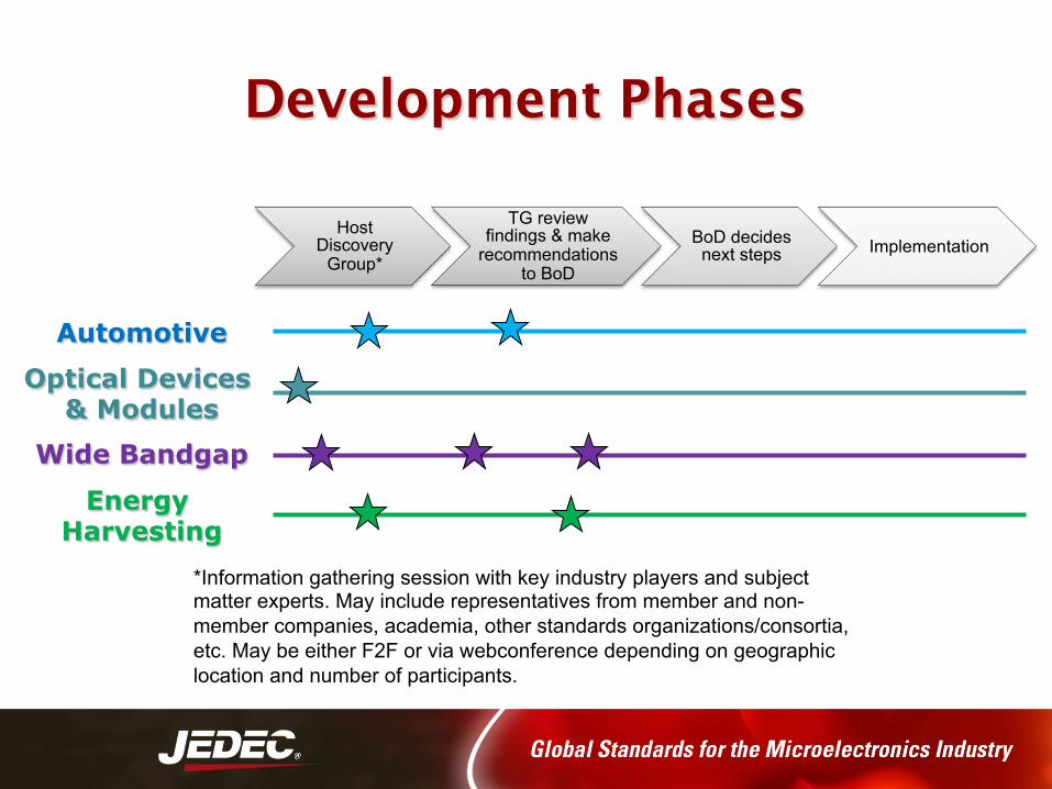
Development Phases
Host Discovery
Group*
TG review findings & make
recommendations to BoD
BoD decides next steps Implementation
Automotive
*Information gathering session with key industry players and subject matter experts. May include representatives from member and non-member companies, academia, other standards organizations/consortia, etc. May be either F2F or via webconference depending on geographic location and number of participants.
Energy Harvesting
Optical Devices & Modules
Wide Bandgap
Wide Bandgap Semiconductors Focus Group Report
Perry Keller
Keysight Technologies Focus Group Chair
JEDEC All-Member Update
June 8, 2016
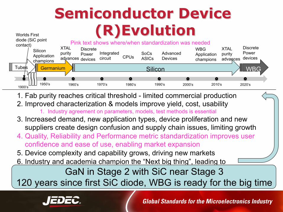
Semiconductor Device (R)Evolution
1. Fab purity reaches critical threshold - limited commercial production 2. Improved characterization & models improve yield, cost, usability
1. Industry agreement on parameters, models, test methods is essential 3. Increased demand, new application types, device proliferation and new
suppliers create design confusion and supply chain issues, limiting growth 4. Quality, Reliability and Performance metric standardization improves user
confidence and ease of use, enabling market expansion 5. Device complexity and capability grows, driving new markets 6. Industry and academia champion the “Next big thing”, leading to
1950’s 1960’s 1970’s 1980’s 1990’s 2000’s 2010’s 2020’s
Discrete Power devices
Germanium Silicon
WBG Application champions
WBG
SoCs ASICs
Silicon Application champions
Integrated circuit
Discrete Power devices
1900’s
Worlds First diode (SiC point contact)
XTAL purity advances
XTAL purity advances CPUs
Advanced Devices
Tubes
GaN in Stage 2 with SiC near Stage 3 120 years since first SiC diode, WBG is ready for the big time
Pink text shows where/when standardization was needed
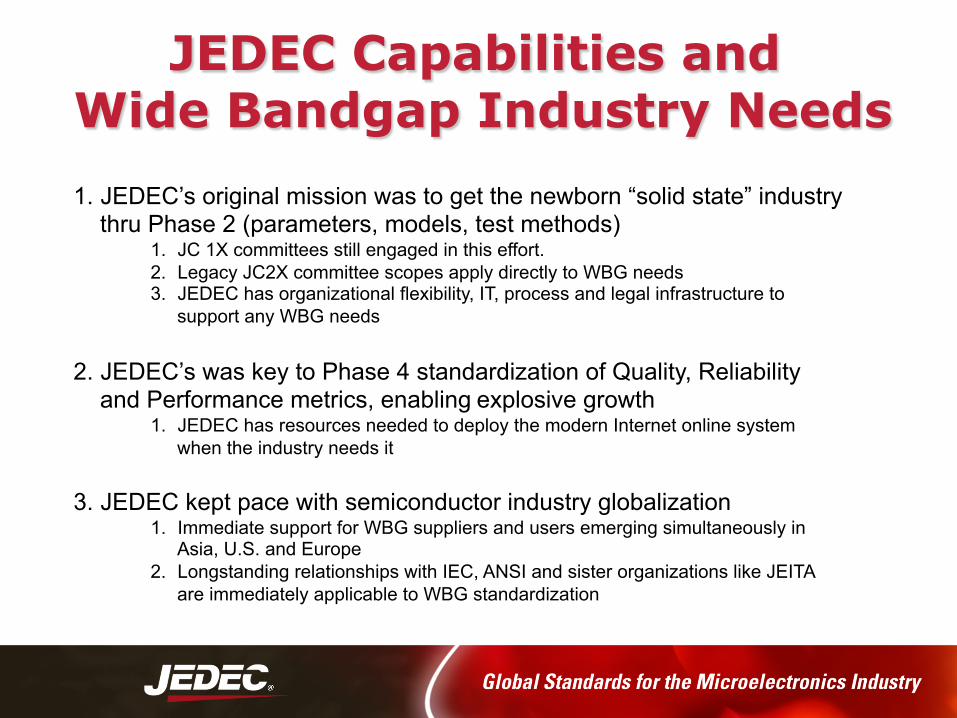
JEDEC Capabilities and Wide Bandgap Industry Needs 1. JEDEC’s original mission was to get the newborn “solid state” industry
thru Phase 2 (parameters, models, test methods) 1. JC 1X committees still engaged in this effort. 2. Legacy JC2X committee scopes apply directly to WBG needs 3. JEDEC has organizational flexibility, IT, process and legal infrastructure to
support any WBG needs
2. JEDEC’s was key to Phase 4 standardization of Quality, Reliability and Performance metrics, enabling explosive growth
1. JEDEC has resources needed to deploy the modern Internet online system when the industry needs it
3. JEDEC kept pace with semiconductor industry globalization
1. Immediate support for WBG suppliers and users emerging simultaneously in Asia, U.S. and Europe
2. Longstanding relationships with IEC, ANSI and sister organizations like JEITA are immediately applicable to WBG standardization
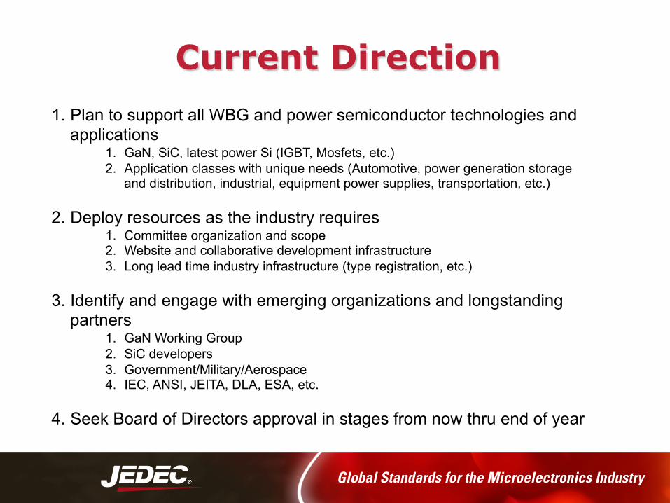
Current Direction 1. Plan to support all WBG and power semiconductor technologies and
applications 1. GaN, SiC, latest power Si (IGBT, Mosfets, etc.) 2. Application classes with unique needs (Automotive, power generation storage
and distribution, industrial, equipment power supplies, transportation, etc.)
2. Deploy resources as the industry requires 1. Committee organization and scope 2. Website and collaborative development infrastructure 3. Long lead time industry infrastructure (type registration, etc.)
3. Identify and engage with emerging organizations and longstanding partners
1. GaN Working Group 2. SiC developers 3. Government/Military/Aerospace 4. IEC, ANSI, JEITA, DLA, ESA, etc.
4. Seek Board of Directors approval in stages from now thru end of year
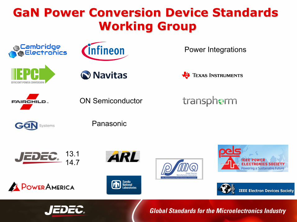
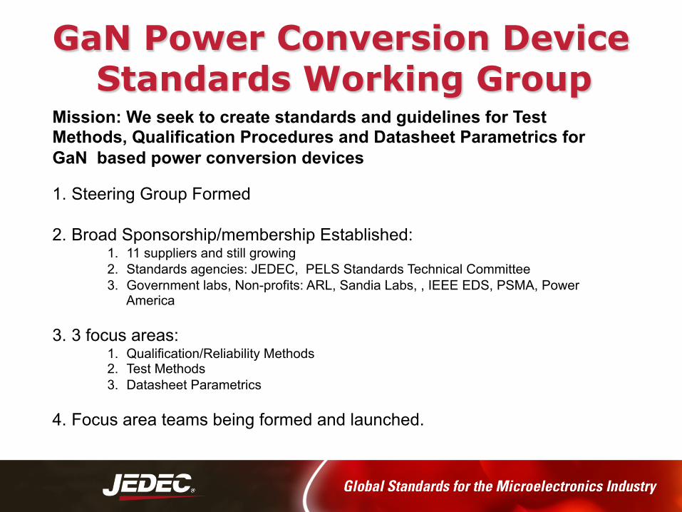
GaN Power Conversion Device Standards Working Group
Panasonic
ON Semiconductor
Power Integrations
13.1 14.7
GaN Power Conversion Device Standards Working Group
Mission: We seek to create standards and guidelines for Test Methods, Qualification Procedures and Datasheet Parametrics for GaN based power conversion devices 1. Steering Group Formed
2. Broad Sponsorship/membership Established:
1. 11 suppliers and still growing 2. Standards agencies: JEDEC, PELS Standards Technical Committee 3. Government labs, Non-profits: ARL, Sandia Labs, , IEEE EDS, PSMA, Power
America
3. 3 focus areas: 1. Qualification/Reliability Methods 2. Test Methods 3. Datasheet Parametrics
4. Focus area teams being formed and launched.
Automotive Initiative Focus Group Report
Hung Vuong Qualcomm
Focus Group Co-Chair
JEDEC All-Member Update June 8, 2016
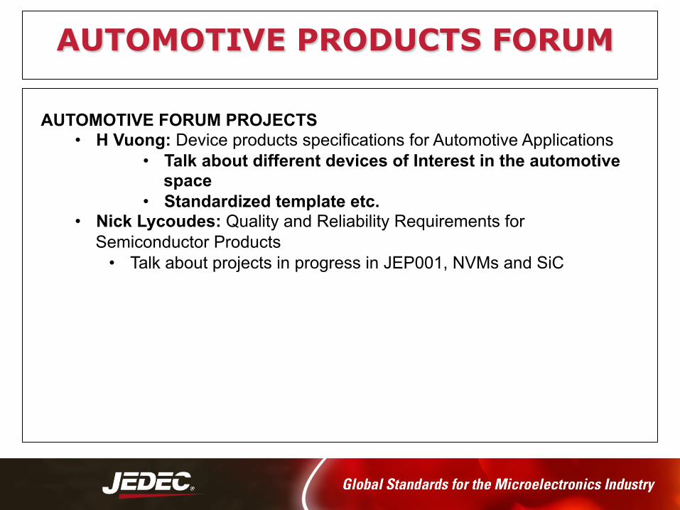
AUTOMOTIVE FORUM PROJECTS • H Vuong: Device products specifications for Automotive Applications
• Talk about different devices of Interest in the automotive space
• Standardized template etc. • Nick Lycoudes: Quality and Reliability Requirements for
Semiconductor Products • Talk about projects in progress in JEP001, NVMs and SiC
AUTOMOTIVE PRODUCTS FORUM
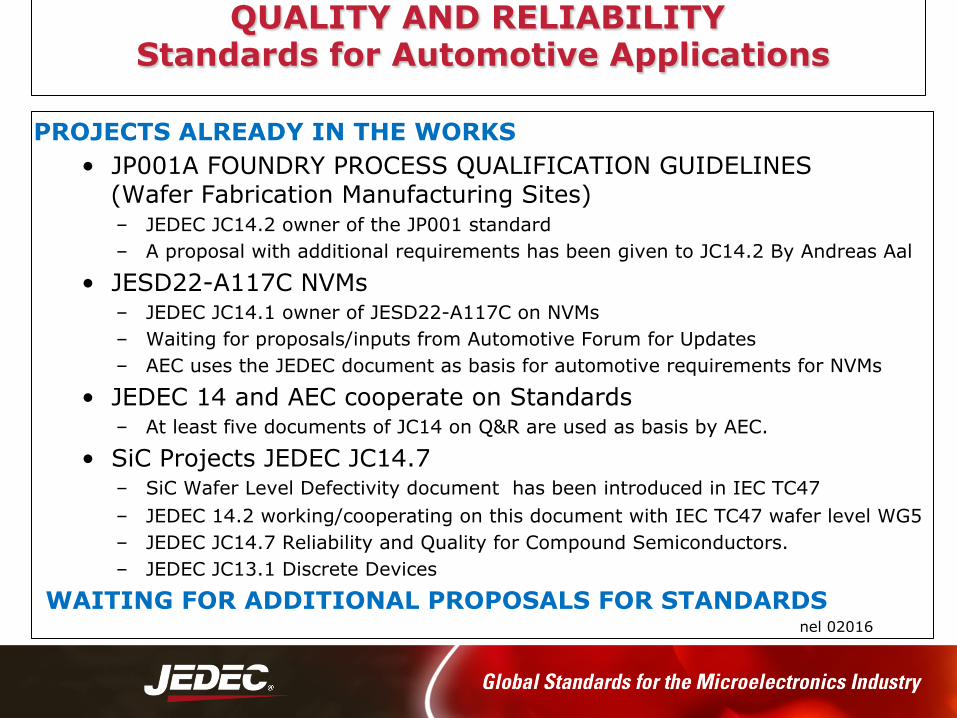
PROJECTS ALREADY IN THE WORKS • JP001A FOUNDRY PROCESS QUALIFICATION GUIDELINES
(Wafer Fabrication Manufacturing Sites) – JEDEC JC14.2 owner of the JP001 standard – A proposal with additional requirements has been given to JC14.2 By Andreas Aal
• JESD22-A117C NVMs – JEDEC JC14.1 owner of JESD22-A117C on NVMs – Waiting for proposals/inputs from Automotive Forum for Updates – AEC uses the JEDEC document as basis for automotive requirements for NVMs
• JEDEC 14 and AEC cooperate on Standards – At least five documents of JC14 on Q&R are used as basis by AEC.
• SiC Projects JEDEC JC14.7 – SiC Wafer Level Defectivity document has been introduced in IEC TC47 – JEDEC 14.2 working/cooperating on this document with IEC TC47 wafer level WG5 – JEDEC JC14.7 Reliability and Quality for Compound Semiconductors. – JEDEC JC13.1 Discrete Devices
WAITING FOR ADDITIONAL PROPOSALS FOR STANDARDS nel 02016
QUALITY AND RELIABILITY Standards for Automotive Applications
TG Summary of Energy Transfer Interface
June 8, 2016
K.C. Chen / Wintec (TG Chair)
A Wasteful AC World
Energy waste. e-Waste. Inconvenience - various adaptors for various devices. Expensive – extra cost for adaptor. Three wires (vs. two wires) It is time to standardize DC energy transfer for the transition to DC world.
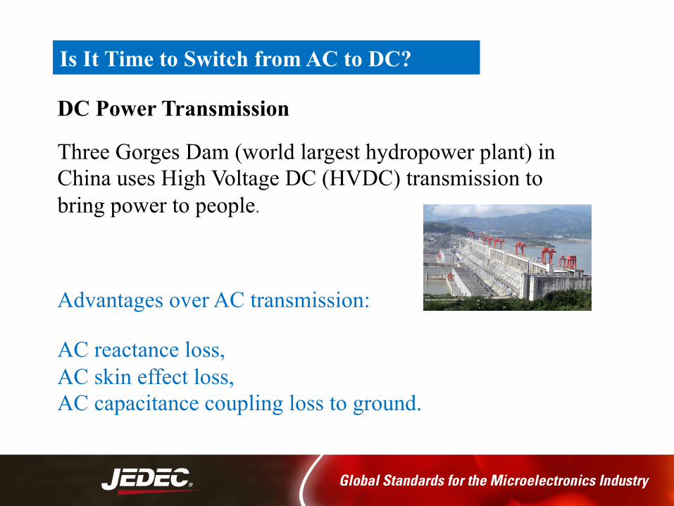
Three Gorges Dam (world largest hydropower plant) in China uses High Voltage DC (HVDC) transmission to bring power to people. Advantages over AC transmission: AC reactance loss, AC skin effect loss, AC capacitance coupling loss to ground.
Is It Time to Switch from AC to DC?
DC Power Transmission
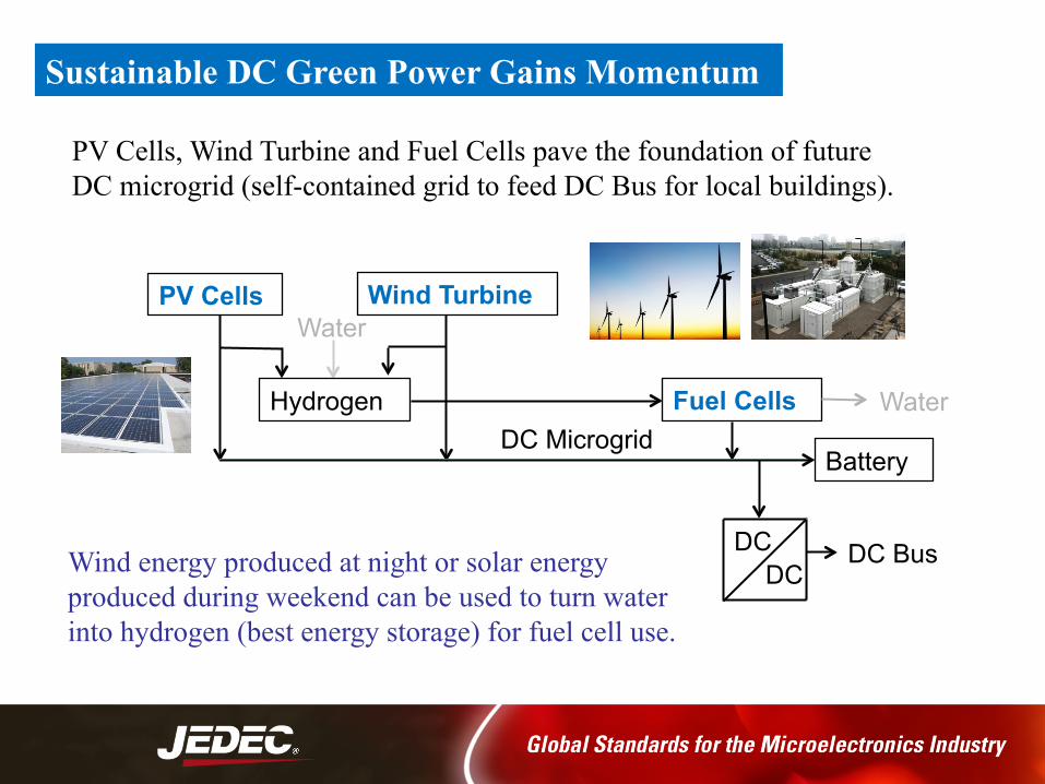
Sustainable DC Green Power Gains Momentum
PV Cells, Wind Turbine and Fuel Cells pave the foundation of future DC microgrid (self-contained grid to feed DC Bus for local buildings).
Wind energy produced at night or solar energy produced during weekend can be used to turn water into hydrogen (best energy storage) for fuel cell use.
PV Cells Wind Turbine
Fuel Cells Hydrogen
Water
Water
Battery
DC Bus DC DC
DC Microgrid
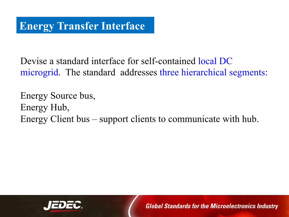
Energy Transfer Interface
Devise a standard interface for self-contained local DC microgrid. The standard addresses three hierarchical segments: Energy Source bus, Energy Hub, Energy Client bus – support clients to communicate with hub.
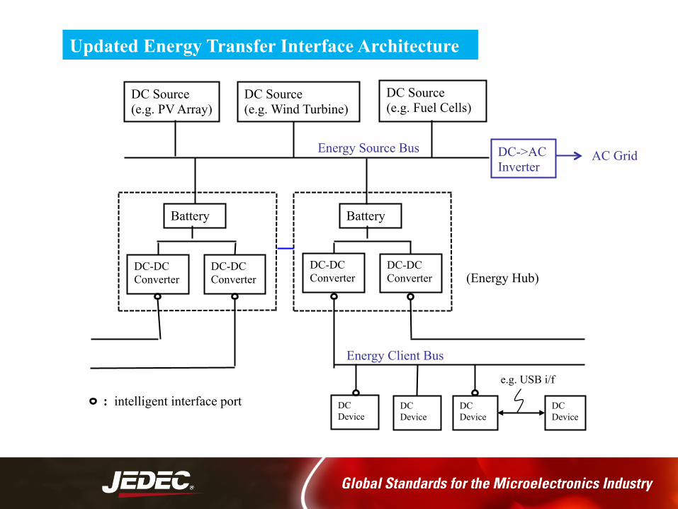
Updated Energy Transfer Interface Architecture
DC Source (e.g. PV Array)
DC-DC Converter
DC Device
DC Device
DC Device
AC Grid
e.g. USB i/f
DC-DC Converter
DC-DC Converter
DC-DC Converter (Energy Hub)
: intelligent interface port
Energy Source Bus
Energy Client Bus
DC->AC Inverter
DC Source (e.g. Wind Turbine)
DC Source (e.g. Fuel Cells)
DC Device
Battery Battery
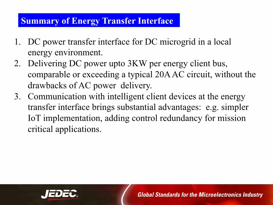
Summary of Energy Transfer Interface
1. DC power transfer interface for DC microgrid in a local energy environment. 2. Delivering DC power upto 3KW per energy client bus,
comparable or exceeding a typical 20A AC circuit, without the drawbacks of AC power delivery.
3. Communication with intelligent client devices at the energy transfer interface brings substantial advantages: e.g. simpler IoT implementation, adding control redundancy for mission critical applications.
Thank You
For Helping The Blue Planet.