JEDEC STANDARD - Micron Technology
52
JEDEC SOLID STATE TECHNOLOGY ASSOCIATION JESD230B JULY 2014 JEDEC STANDARD NAND Flash Interface Interoperability (Revision of JESD2320A, August 2013)
Transcript of JEDEC STANDARD - Micron Technology
JEDEC SOLID STATE TECHNOLOGY ASSOCIATION
JESD230B
JULY 2014
JEDECSTANDARD
NAND Flash Interface Interoperability
(Revision of JESD2320A, August 2013)

P LE A S E !
D O N ’T V IO LA T E T H E
LA W !
T his docum ent is copyrigh ted by JE D E C and m ay not be reproduced w ithout perm ission.
For in form ation , contact:
JE D E C S olid S tate T echnology A ssociation 3103 N orth 10th S treet
S uite 240 South A rlington , V A 22201-2107
o r refer to w w w .jedec.org under S tandards-D ocum ents/C opyright In form ation

NOTICE
JEDEC standards and publications contain material that has been prepared, reviewed, and approved
through the JEDEC Board of Directors level and subsequently reviewed and approved by the JEDEC legal
counsel.
JEDEC standards and publications are designed to serve the public interest through eliminating
misunderstandings between manufacturers and purchasers, facilitating interchangeability and
improvement of products, and assisting the purchaser in selecting and obtaining with minimum delay the
proper product for use by those other than JEDEC members, whether the standard is to be used either
domestically or internationally.
JEDEC standards and publications are adopted without regard to whether or not their adoption may
involve patents or articles, materials, or processes. By such action JEDEC does not assume any liability to
any patent owner, nor does it assume any obligation whatever to parties adopting the JEDEC standards or
publications.
The information included in JEDEC standards and publications represents a sound approach to product
specification and application, principally from the solid state device manufacturer viewpoint. Within the
JEDEC organization there are procedures whereby a JEDEC standard or publication may be further
processed and ultimately become an ANSI standard.
No claims to be in conformance with this standard may be made unless all requirements stated in the
standard are met.
Inquiries, comments, and suggestions relative to the content of this JEDEC standard or publication should
be addressed to JEDEC at the address below, or refer to www.jedec.org under Standards and Documents
for alternative contact information.
Published by
©JEDEC Solid State Technology Association 2014
3103 North 10th Street
Suite 240 South
Arlington, VA 22201-2107
This document may be downloaded free of charge; however JEDEC retains the copyright on this material.
By downloading this file the individual agrees not to charge for or resell the resulting material.
PRICE: Contact JEDEC
Printed in the U.S.A.
All rights reserved


JEDEC Standard No. 230BPage 1
NAND FLASH INTERFACE INTEROPERABILITY
(From JEDEC Board Ballot JCB-14-16, formulated under the cognizance of the JC-42.4 Subcommittee on Nonvolatile Memory Devices.)
1 Scope
This standard was jointly developed by JEDEC and the Open NAND Flash Interface Workgroup, hereafter referred to as ONFI. This standard defines a standard NAND flash device interface interoperability standard that provides means for system be designed that can support Asynchronous SDR, Synchronous DDR and Toggle DDR NAND flash devices that are interoperable between JEDEC and ONFI member implementations.
2 Terms, definitions, abbreviations and conventions
2.1 Terms and definitions
address: A character or group of characters that identifies a register, a particular part of storage, or some other data source or destination. (Ref. ANSI X3.172 and JESD88.) NOTE 1 In a nonvolatile memory array, the address consists of characters, typically hexadecimal, to identify the row and column location of the memory cell(s). NOTE 2 For NAND nonvolatile memory devices, the row address is for a page, block, or logical unit number (LUN); the column address is for the byte or word within a page.
NOTE 3 The least significant bit of the column address is zero for the source synchronous data interface.
asynchronous: Describing operation in which the timing is not controlled by a clock. NOTE For a NAND nonvolatile memory, asynchronous also means that data is latched with the WE_n signal for the write operation and the RE_n signal for the read operation.
block: A continuous range of memory addresses. (Ref. IEC 748-2 and JESD88.)
NOTE 1 The number of addresses included in the range is frequently equal to 2n, where n is the number of bits in the address. NOTE 2 For nonvolatile memories, a block consists of multiple pages and is the smallest addressable memory segment within a memory device for the erase operation.
column: In a nonvolatile memory array, a series of memory cells whose sources and/or drains are connected via a bit line. NOTE 1 Depending on the nonvolatile memory array, the bit line is accessed via the column select transistor, the column address decoder, or other decoding scheme. NOTE 2 In nonvolatile memory device, a column decoder accesses a bit (x1), byte (x8), word (x16), or Dword (x32) either individually or within a page. NOTE 3 In a typical schematic of a memory array, the column is in the vertical direction.
Dword (x32): A sequence of 32 bits that is stored, addressed, transmitted, and operated on as a unit within a computing system. NOTE 1 A Dword may be represented as 32 bits, as two adjacent words, or as four adjacent bytes. When shown as bits, the least significant bit is bit 0 and the most significant bit is bit 31; the most significant bit is shown on the left. When shown as words, the least significant word (lower) is word 0 and the most significant (upper) word is word 1. When shown as bytes, the least significant byte is byte 0 and the most significant byte is byte 3. NOTE 2 See Figure 1 for a description of the relationship between bytes, words, and Dwords.

JEDEC Standard No. 230BPage 2
2.1 Terms and definitions (cont’d)
latching edge: The rising or falling edge of a waveform that initiates a latch operation. NOTE 1 For a NAND nonvolatile memory the latching edge is the edge of the CK or DQS signal on which the contents of the data bus are latched for the source synchronous data interface. NOTE 2 For a NAND nonvolatile data cycles, the latching edge is both the rising and falling edges of the DQS signal. NOTE 3 For a NAND nonvolatile command and address cycles, the latching edge for the source synchronous interface is the rising edge of the CK signal.
NAND defect area: A designated location within the NAND memory where factory defects are identified by the manufacturer.NOTE 1 The location is a portion of either the first page and/or the last page of the factory-marked defect block, this defect area in each page is defined as (# of data bytes) to (# of data bytes + # of spare bytes -1). NOTE 2 For an 8-bit data access NAND memory device, the manufacturer sets the first byte in the defect area of the first or last page of the defect block to a value of 00h.NOTE 3 For a 16-bit data access NAND memory device, the manufacturer sets the first word in the defect area of the first or last page of the defect block to a value of 0000h.
NAND nonvolatile memory device: The packaged NAND nonvolatile memory unit containing one or more NAND targets. NOTE This is referred to as "device" in this standard.
NAND row address: An address referencing the LUN, block, and page to be accessed.NOTE 1 The page address uses the least significant row address bits.NOTE 2 The block address uses the middle row address bits.NOTE 3 The LUN address uses the most significant row address bits.
page: The smallest nonvolatile memory array segment, within a device, that can be addressed for read or program operations.
page register: A register used to transfer data from a page in the memory array for a read operation or to transfer data to a page in the memory array for a program operation.
read request (for a nonvolatile memory): A data output cycle request from the host that results in a data transfer from the device to the host.
source synchronous (for a nonvolatile memory): Describing an operation in which the strobe signal (DQS) is transmitted with the data to indicate when the data should be latched. NOTE The strobe signal (DQS) is similar in concept to an additional data bus bit.
status register (SR[x]): A register within a particular LUN containing status information about that LUN. NOTE SR[x] refers to bit "x" within the status register.
target: A nonvolatile memory component with a unique chip enable (CE_n) select pin.
word (x16): A sequence of 16 bits that is stored, addressed, transmitted, and operated on as a unit within a computing system.NOTE 1 A word may be represented as 16 bits or as two adjacent bytes. When shown as bits, the least significant bit is bit 0 and the most significant bit is bit 15; the most significant bit is shown on the left. When shown as bytes, the least significant byte (lower) is byte 0 and the most significant byte is byte 2. NOTE 2 See Figure 1 for a description of the relationship between bytes, words, and Dwords.

JEDEC Standard No. 230BPage 3
2.2 Abbreviations
DDR: Abbreviation for "double data rate".
LUN (logical unit number): The minimum memory array size that can independently execute commands and report status.
N/A: Abbreviation for "not applicable". Fields marked as "na" are not used.
O/M: Abbreviation for Optional/Mandatory requirement. When the entry is set to "M", the item is mandatory. When the entry is set to "O", the item is optional.
2.3 Conventions
2.3.1 Active-low signals
While the preferred method for indicating a signal that is active when low is to use the over-bar as in CE, the difficulty in producing this format has resulted in several alternatives meant to be equivalents. These are the use of a CE reverse solidus ( \ ) or the trailing underscore ( _ ) following the signal name as in CE\ and CE_. In this publication "_n" is used to indicate an active low signal (i.e. an inverted logic sense).
2.3.2 Signal names
The names of abbreviations, initials, and acronyms used as signal names are in all uppercase (e.g., CE_n). Fields containing only one bit are usually referred to as the "name bit" instead of the "name field". Numerical fields are unsigned unless otherwise indicated.
2.3.3 Precedence in case of conflict
If there is a conflict between text, figures, state machines, timing diagrams, and/or tables, the precedence shall be state machine, timing diagrams, tables, figures, and text.
2.4 Keywords
Several keywords are used to differentiate between different levels of requirements or suggestions.
mandatory: A keyword indicating items to be implemented as defined by a standard. Users are required to implement all such mandatory requirements to ensure interoperability with other products that conform to the standard.
may: A keyword that indicates flexibility of choice between stated alternatives or possibly nothing with no implied preference.
optional: A keyword that describes features that are not required by the specification. However, if any optional feature defined by the specification is implemented, that feature shall be implemented in the way defined by the specification.
reserved: A keyword indicating reserved bits, bytes, words, fields, and opcode values that are set-aside for future standardization. Their use and interpretation may be specified by future extensions to this or other specifications. A reserved bit, byte, word, or field may be cleared to zero or in accordance with a future extension to this publication. A host should not read/use reserved information.
shall: A keyword indicating a mandatory requirement.
should: A keyword indicating flexibility of choice with a strongly preferred alternative. This is equivalent to the phrase "it is recommended".

JEDEC Standard No. 230BPage 4
2.5 Byte, Word and Dword Relationships
Figure 1 illustrates the relationship between bytes, words and Dwords
Figure 1 — Byte, word and Dword relationships
7
6
5
4
3
2
1
0
Byte 1
514
13
12
11
10
9
8
7
6
5
4
3
2
1
0
Word Byte 1 Byte 0 31
30
29
28
27
26
25
24
23
22
21
20
19
18
17
16
15
14
13
12
11
10
9
8
7
6
5
4
3
2
1
0
Dword
Word 1 Word 0
Byte 3 Byte 2 Byte 1 Byte 0

JEDEC Standard No. 230BPage 5
2.6 Pin description
Table 1 — Pin description
NameInput/Output
Description
IO0 ~ IO7(~ IO15)DQ0 ~ DQ7
DQ0_x ~ DQ7_xI/O
DATA INPUTS/OUTPUTS These signals are used to input command, address and data, and to output data during read operations. The signals float to high-z when the chip is deselected or when the outputs are disabled. IO0 ~ IO15 are used in a 16-bit wide target configuration. With multi channel support, IO0_0~IO7_0 and IO0_1~IO7_1 are used for IOs of channel 0 and IOs of channel 1 respectively. Also known as DQ0~DQ7 for Toggle DDR and Synchronous DDR. The number after the underscore represents the channel. For example, DQ0_0 indicates DQ0 of channel-0 and DQ0_1 does DQ0 of channel-1.
CLE_x ICOMMAND LATCH ENABLEThe CLE_x signal is one of the signals used by the host to indicate the type of bus cycle (command, address, data).
ALE_x IADDRESS LATCH ENABLEThe ALE_x signal is one of the signals used by the host to indicate the type of bus cycle (command, address, data).
CEx_x_n I
CHIP ENABLEThe CEx_x_n input is the target selection control. When CEx_x_n is high and the target is in the ready state, the target goes into a low-power standby state. When CEx_x_n is low, the target is selected. The number after the first underscore represents the channel. For example, CE0_0_n indicates CE0_n of channel-0 and CE0_1_n does CE0_n of channel-1.
WE_x_n I
WRITE ENABLEThe WE_x_n input controls writes to the I/O port. For Asynchronous SDR Data, commands, addresses are latched on the rising edge of the WE_x_n pulse. For Toggle DDR commands, addresses are latched on the rising edge of the WE_x_n pulse.
R/B_x_n O
READY/BUSY OUTPUTThe R/B_x_n output indicates the status of the target operation. When low, it indicates that one or more operations are in progress and returns to high state upon completion. It is an open drain output and does not float to high-z condition when the chip is deselected or when outputs are disabled.
RE_x_n(RE_x_t)
I
READ ENABLEThe RE_x_n input is the serial data-out control. For Asynchronous SDR Data is valid tREA after the falling edge and for Toggle DDR Data is valid after the falling edge & rising edge of RE_x_n which also increments the internal column address counter by each one.
RE_x_c IComplement of Read EnableThis is the complementary signal to Read Enable
DQS_x(DQS_x_t)
I/O
Data StrobeThe data strobe signal that indicates the data valid window for Toggle DDR and Synchronous DDR data interface. Output with read data, input with write data. Edge-aligned with read data, centered in write data.
DQS_x_c I/OComplement of Data StrobeThis is the complementary signal to Data Strobe.
W/R_x I
Write/Read DirectionThe Write/Read Direction signal indicates the owner of the DQ bus and DQS signal in the Synchronous DDR data interface. This signal shares the same pin as RE_x_n in the asynchronous data interface.

JEDEC Standard No. 230BPage 6
NOTE 1 All Vcc, VccQ and Vss pins of each device shall be connected to common power supply outputs.NOTE 2 All Vcc, VccQ, Vss and VssQ shall not be disconnected.
3 VccQ
Lower voltage is generally more preferred for high speed operation in terms of signal integrity and power consumption. 1.2V VccQ is recommended to enable speeds up to 800Mbps. A NAND device shall support at least one of 3.3V VccQ or 1.8V VccQ or 1.2V VccQ.
CK_x IClockThe Clock signal is used as the clock in Synchronous DDR data interface. This signal shares the same pin as WE_x_n in the asynchronous data interface.
WP_x_n IWRITE PROTECTThe WP_x_n disables the Flash array program and erase operations.
Vcc IPOWERVCC is the power supply for device.
VccQ II/O POWERThe VccQ is the power supply for input and/or output signals.
Vss IGROUNDThe Vss signal is the power supply ground.
VssQ II/O GROUNDThe VssQ signal is the ground for input and/or output signals
VSPx n/a
Vendor SpecificThe function of these signals is defined and specified by the NAND vendor. Any VSP signal not used by the NAND vendor shall not be connected internal to the device.
VREFQ n/aReference voltageThis is used as an external voltage reference.
RZQ_x SupplyReference pin for ZQ calibrationThis is used on ZQ calibration and RZQ ball shall be connected to Vss through 300ohm resistor
ENi / ENo I/OEnumeration pins These pins may be used for ONFI NAND
R n/aReservedThese pins shall not be connected by host.
RFU n/aReserved For Future useThese pins may be assigned for certain functions in the future
NU n/aNot Usable A pin that is not to be used in normal applications and that may or may not have an internal connection.
NC n/a
No (internal) connection A pin that has no internal connection and that can be used as a support for external wiring without disturbing the function of the device, provided that the voltage applied to this terminal (by means of wiring) does not exceed the highest supply voltage rating of the circuit.

JEDEC Standard No. 230BPage 7
3.1 Operating Voltage Range
Table 2 — Recommended DC operating conditions
Parameter Symbol Min. Typ. Max. Unit
3.2 AC/DC operating condition
Table 3 — Single-Ended AC and DC Input Levels for control signals1) and DQ-related signals2)
Parameter Symbol Min. Max. Unit
NOTE 1 Control signals are CE_n, WE_n, WP_n, ALE and CLENOTE 2 DQ-related signals are RE_n, DQS_n, DQs NOTE 3 Refer to vendor specification
Supply Voltage for 3.3V I/O signaling VccQ 2.7 3.3 3.6
VSupply Voltage for 1.8V I/O signaling VccQ 1.7 1.8 1.95
Supply Voltage for 1.2V I/O signaling VccQ 1.14 1.2 1.26
Ground Voltage for I/O signaling VssQ 0 0 0
DC input high for control signals1) VIH.CNT(DC) 0.7*VCCQ VCCQ
V
DC input low for control signals1) VIL.CNT(DC) VSSQ 0.3*VCCQ
AC input high for control signals1) VIH.CNT(AC) 0.8*VCCQOvershoot
spec
AC input low for control signals1) VIL.CNT(AC)Undershoot
spec0.2*VCCQ
DC input high for DQ-related signals2) w/o VREFQ
VIH.DQ(DC) 0.7*VCCQ VCCQ
DC input low for DQ-related signals2) w/o VREFQ
VIL.DQ(DC) VSSQ 0.3*VCCQ
AC input high for DQ-related signals2) w/o VREFQ
VIH.DQ(AC) 0.8*VCCQOvershoot
spec
AC input low for DQ-related signals2) w/o VREFQ
VIL.DQ(AC)Undershoot
spec0.2*VCCQ
DC input high for DQ-related signals2) w/ VREFQ (1.8V VccQ)
VIH.DQ(DC) Note 3) VCCQ
DC input low for DQ-related signals2) w/ VREFQ (1.8V VccQ)
VIL.DQ(DC) VSSQ Note 3)
AC input high for DQ-related signals2) w/ VREFQ (1.8V VccQ)
VIH.DQ(AC) Note 3) Note 3)
AC input low for DQ-related signals2) w/ VREFQ (1.8V VccQ)
VIL.DQ(AC) Note 3) Note 3)
DC input high for DQ-related signals2) w/ VREFQ (1.2V VccQ)
VIH.DQ(DC)VREFQ
+0.1VCCQ
DC input low for DQ-related signals2) w/ VREFQ (1.2V VccQ)
VIL.DQ(DC) VSSQVREFQ
-0.1
AC input high for DQ-related signals2) w/ VREFQ (1.2V VccQ)
VIH.DQ(AC)VREFQ
+0.15Overshoot
spec
AC input low for DQ-related signals2) w/ VREFQ (1.2V VccQ)
VIL.DQ(AC)Undershoot
specVREFQ
-0.15
JEDEC Standard No. 230BPage 8
3.2 AC/DC operating condition (cont’d)
Table 4 — Single-Ended AC and DC Output Levels for control signals1) and DQ-related signals2)
Parameter Symbol Min. Max. Unit
NOTE 1 Control signals are R/B_nNOTE 2 DQ-related signals are DQS_n, DQs
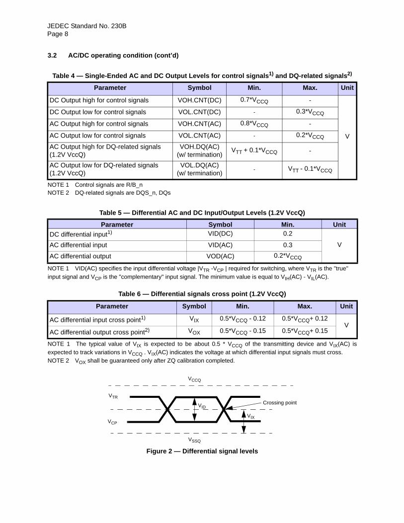
Table 5 — Differential AC and DC Input/Output Levels (1.2V VccQ)
Parameter Symbol Min. Unit
NOTE 1 VID(AC) specifies the input differential voltage |VTR -VCP | required for switching, where VTR is the "true"
input signal and VCP is the "complementary" input signal. The minimum value is equal to VIH(AC) - VIL(AC).
Table 6 — Differential signals cross point (1.2V VccQ)
Parameter Symbol Min. Max. Unit
NOTE 1 The typical value of VIX is expected to be about 0.5 * VCCQ of the transmitting device and VIX(AC) is
expected to track variations in VCCQ . VIX(AC) indicates the voltage at which differential input signals must cross.
NOTE 2 VOX shall be guaranteed only after ZQ calibration completed.
VCCQ
Crossing point
VSSQ
VTR
VCP
VID
VIX
Figure 2 — Differential signal levels
DC Output high for control signals VOH.CNT(DC) 0.7*VCCQ -
V
DC Output low for control signals VOL.CNT(DC) - 0.3*VCCQ
AC Output high for control signals VOH.CNT(AC) 0.8*VCCQ -
AC Output low for control signals VOL.CNT(AC) - 0.2*VCCQ
AC Output high for DQ-related signals(1.2V VccQ)
VOH.DQ(AC)(w/ termination)
VTT + 0.1*VCCQ -
AC Output low for DQ-related signals(1.2V VccQ)
VOL.DQ(AC)(w/ termination)
- VTT - 0.1*VCCQ
DC differential input1) VID(DC) 0.2
VAC differential input VID(AC) 0.3
AC differential output VOD(AC) 0.2*VCCQ
AC differential input cross point1) VIX 0.5*VCCQ - 0.12 0.5*VCCQ+ 0.12V
AC differential output cross point2) VOX 0.5*VCCQ - 0.15 0.5*VCCQ+ 0.15
JEDEC Standard No. 230BPage 9
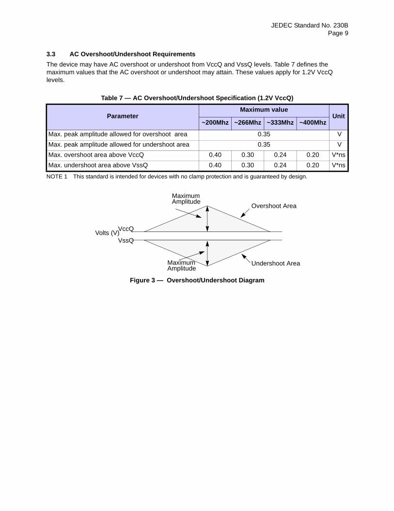
3.3 AC Overshoot/Undershoot Requirements
The device may have AC overshoot or undershoot from VccQ and VssQ levels. Table 7 defines the maximum values that the AC overshoot or undershoot may attain. These values apply for 1.2V VccQ levels.
Table 7 — AC Overshoot/Undershoot Specification
ParameterMaximum value
Unit~200Mhz ~266Mhz ~333Mhz ~400Mhz
(1.2V VccQ)
NOTE 1 This standard is intended for devices with no clamp protection and is guaranteed by design.
Figure 3 — Overshoot/Undershoot Diagram
Max. peak amplitude allowed for overshoot area 0.35 V
Max. peak amplitude allowed for undershoot area 0.35 V
Max. overshoot area above VccQ 0.40 0.30 0.24 0.20 V*ns
Max. undershoot area above VssQ 0.40 0.30 0.24 0.20 V*ns
Overshoot Area
Undershoot Area
MaximumAmplitude
MaximumAmplitude
VccQ
VssQVolts (V)

JEDEC Standard No. 230BPage 10
4 Package and Addressing
4.1 BGA-63 (Single x8 / x16 BGA)
Figure 4 defines the ball assignments for devices using NAND Single x8 / x16 BGA packaging with 8-bit data access for the asynchronous SDR data interface. Figure 5 defines the ball assignments for devices using NAND Single x8 / x16 BGA packaging with 8-bit data access for the synchronous DDR data interface. Figure 6 defines the ball assignments for devices using NAND Single x8 / x16 BGA packaging with 16-bit data access for the asynchronous SDR data interface. The NAND Single x8/x16 BGA package with 16-bit data access does not support the Synchronous DDR data interface.
This package uses MO-201
Figure 4 — Ball assignments for 8-bit data access, asynchronous SDR only data interface
1 2 3 4 5 6 7 8 9 10
A NC NC NC NC
B NC NC NC
C WP_n ALE VSS CE0_n WE_n R/B0_n
D VCC RE_n CLE CE1_n CE2_n R/B1_n
E NC NC NC NC CE3_n R/B2_n
F NC NC NC NC VSS R/B3_n
G VSP3 VCC VSP1 NC NC VSP2
H NC IO0 NC NC NC VCCQ
J NC IO1 NC VCCQ IO5 IO7
K VSSQ IO2 IO3 IO4 IO6 VSSQ
L NC NC NC NC
M NC NC NC NC
JEDEC Standard No. 230BPage 11
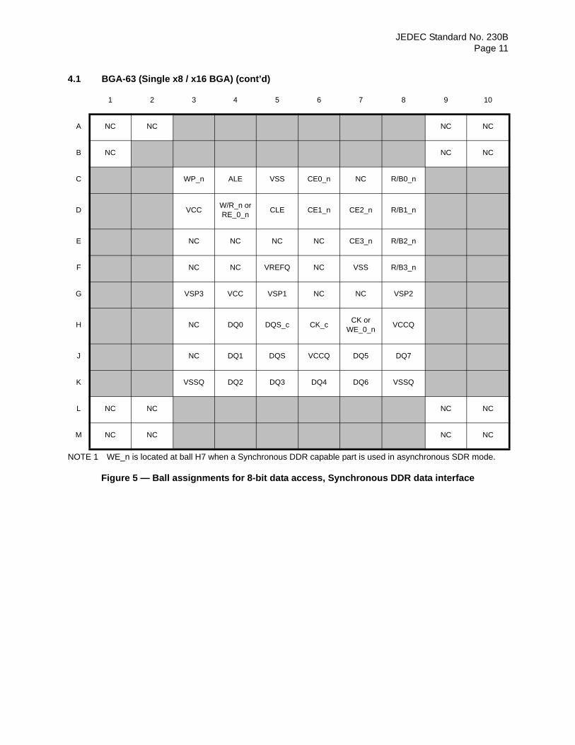
4.1 BGA-63 (Single x8 / x16 BGA) (cont’d)
NOTE 1 WE_n is located at ball H7 when a Synchronous DDR capable part is used in asynchronous SDR mode.
Figure 5 — Ball assignments for 8-bit data access, Synchronous DDR data interface
1 2 3 4 5 6 7 8 9 10
A NC NC NC NC
B NC NC NC
C WP_n ALE VSS CE0_n NC R/B0_n
D VCCW/R_n orRE_0_n
CLE CE1_n CE2_n R/B1_n
E NC NC NC NC CE3_n R/B2_n
F NC NC VREFQ NC VSS R/B3_n
G VSP3 VCC VSP1 NC NC VSP2
H NC DQ0 DQS_c CK_cCK or
WE_0_nVCCQ
J NC DQ1 DQS VCCQ DQ5 DQ7
K VSSQ DQ2 DQ3 DQ4 DQ6 VSSQ
L NC NC NC NC
M NC NC NC NC

JEDEC Standard No. 230BPage 12
4.1 BGA-63 (Single x8 / x16 BGA) (cont’d)
Figure 6 — Ball assignments for 16-bit, asynchronous SDR only data access
1 2 3 4 5 6 7 8 9 10
A NC NC NC NC
B NC NC NC
C WP_n ALE VSS CE0_n WE_n R/B0_n
D VCC RE_n CLE CE1_n CE2_n R/B1_n
E NC NC NC NC CE3_n R/B2_n
F NC NC NC NC VSS R/B3_n
G VSP3 VCC VSP1 IO13 IO15 VSP2
H IO8 IO0 IO10 IO12 IO14 VCCQ
J IO9 IO1 IO11 VCCQ IO5 IO7
K VSSQ IO2 IO3 IO4 IO6 VSSQ
L NC NC NC NC
M NC NC NC NC

JEDEC Standard No. 230BPage 13
4.2 BGA-100 (Dual x8 BGA)
Figure 7 defines the ball assignments for devices using NAND Dual x8 BGA packaging with dual 8-bit data access for the asynchronous SDR data interface. Figure 8 defines the ball assignments for devices using NAND Dual x8 BGA packaging with dual 8-bit data access for the Toggle DDR or Synchronous DDR data interface. The minimum package size is 12x18mm and the maximum package size is 14x18mm.
This package uses MO-304.
Figure 7 — Ball assignments for dual 8-bit data access, asynchronous SDR data interface
1 2 3 4 5 6 7 8 9 10
A R R R R
B R R
C
D R VSP VSP2_1 WP_1_n VSP1_1 VSP0_1 VSP R
E R VSP VSP2_0 WP_0_n VSP1_0 VSP0_0 VSP VDDi
F VCC VCC VCC VCC VCC VCC VCC VCC
G VSS VSS VSS VSS VSS VSS VSS VSS
H VSSQ VCCQ R R R/B0_1_nR/B1_1_n
or ENoVCCQ VSSQ
J IO0_1 IO2_1 ALE_1 CE1_1_n R/B0_0_n R/B1_0_n IO5_1 IO7_1
K IO0_0 IO2_0 ALE_0CE1_0_n
or ENiCE0_1_n CE0_0_n IO5_0 IO7_0
L VCCQ VSSQ VCCQ CLE_1 RE_1_n VCCQ VSSQ VCCQ
M IO1_1 IO3_1 VSSQ CLE_0 RE_0_n VSSQ IO4_1 IO6_1
N IO1_0 IO3_0 NC NC NC WE_1_n IO4_0 IO6_0
P VSSQ VCCQ NC NC NC WE_0_n VCCQ VSSQ
R
T R R
U R R R R
JEDEC Standard No. 230BPage 14
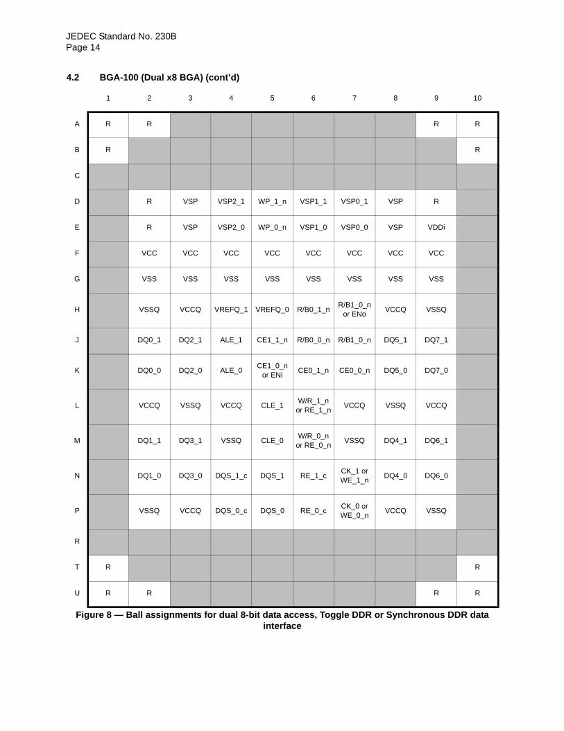
4.2 BGA-100 (Dual x8 BGA) (cont’d)
Figure 8 — Ball assignments for dual 8-bit data access, Toggle DDR or Synchronous DDR data interface
1 2 3 4 5 6 7 8 9 10
A R R R R
B R R
C
D R VSP VSP2_1 WP_1_n VSP1_1 VSP0_1 VSP R
E R VSP VSP2_0 WP_0_n VSP1_0 VSP0_0 VSP VDDi
F VCC VCC VCC VCC VCC VCC VCC VCC
G VSS VSS VSS VSS VSS VSS VSS VSS
H VSSQ VCCQ VREFQ_1 VREFQ_0 R/B0_1_nR/B1_0_n
or ENoVCCQ VSSQ
J DQ0_1 DQ2_1 ALE_1 CE1_1_n R/B0_0_n R/B1_0_n DQ5_1 DQ7_1
K DQ0_0 DQ2_0 ALE_0CE1_0_n
or ENiCE0_1_n CE0_0_n DQ5_0 DQ7_0
L VCCQ VSSQ VCCQ CLE_1W/R_1_n
or RE_1_nVCCQ VSSQ VCCQ
M DQ1_1 DQ3_1 VSSQ CLE_0W/R_0_n
or RE_0_nVSSQ DQ4_1 DQ6_1
N DQ1_0 DQ3_0 DQS_1_c DQS_1 RE_1_cCK_1 orWE_1_n
DQ4_0 DQ6_0
P VSSQ VCCQ DQS_0_c DQS_0 RE_0_cCK_0 orWE_0_n
VCCQ VSSQ
R
T R R
U R R R R
JEDEC Standard No. 230BPage 15
R/ VDDi R R VssQ R
CE1_ R R R R R
R/B1 RE R/ IO7 IO6 IO5 Vcc
Vcc RE Vss IO7 IO5 Vcc
CE CE R/ WP IO6 IO4 IO4
CLE CLE WE IO0 IO2 Vss IO3
Vss ALE WP IO1 IO3 Vss
CE1ALE WE IO0 IO1 IO2 Vcc
A B C D E F G H J K L M N
8
7
6
5
4
3
2
1
0
OA OB OC OD OE OF
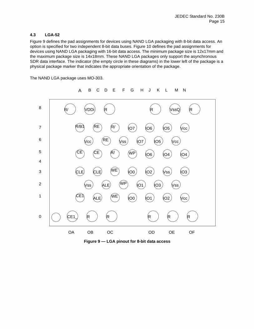
4.3 LGA-52
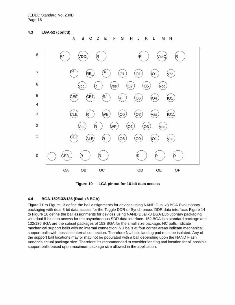
Figure 9 defines the pad assignments for devices using NAND LGA packaging with 8-bit data access. An option is specified for two independent 8-bit data buses. Figure 10 defines the pad assignments for devices using NAND LGA packaging with 16-bit data access. The minimum package size is 12x17mm and the maximum package size is 14x18mm. These NAND LGA packages only support the asynchronous SDR data interface. The indicator (the empty circle in these diagrams) in the lower left of the package is a physical package marker that indicates the appropriate orientation of the package.
The NAND LGA package uses MO-303.
Figure 9 — LGA pinout for 8-bit data access
JEDEC Standard No. 230BPage 16
R/ VDDi R R VssQ R
CE3_ R R R R R
R/ RE_ R/ IO1 IO1 IO1 Vcc
Vcc R Vss IO7 IO5 Vcc
CE0 CE1 R/ R IO6 IO4 IO1
CLE R WE IO0 IO2 Vss IO11
Vss R WP IO1 IO3 Vss
CE2 ALE R IO8 IO9 IO1 Vcc
A B C D E F G H J K L M N
8
7
6
5
4
3
2
1
0
OA OB OC OD OE OF
4.3 LGA-52 (cont’d)
Figure 10 — LGA pinout for 16-bit data access
4.4 BGA-152/132/136 (Dual x8 BGA)
Figure 11 to Figure 13 define the ball assignments for devices using NAND Dual x8 BGA Evolutionary packaging with dual 8-bit data access for the Toggle DDR or Synchronous DDR data interface. Figure 14 to Figure 16 define the ball assignments for devices using NAND Dual x8 BGA Evolutionary packaging with dual 8-bit data access for the asynchronous SDR data interface. 152 BGA is a standard package and 132/136 BGA are the subset packages of 152 BGA for the small size package. NC balls indicate mechanical support balls with no internal connection. NU balls at four corner areas indicate mechanical support balls with possible internal connection. Therefore NU balls landing pad must be isolated. Any of the support ball locations may or may not be populated with a ball depending upon the NAND Flash Vendor's actual package size. Therefore it's recommended to consider landing pad location for all possible support balls based upon maximum package size allowed in the application.

JEDEC Standard No. 230BPage 17
4.4 BGA-152/132/136 (Dual x8 BGA) (cont’d)
The BGA package uses MO-304.
Figure 11 — NAND Dual x8 BGA-152 package ball assignments for dual 8-bit data access, Toggle DDR or Synchronous DDR data interface
1 2 3 4 5 6 7 8 9 10 11 12 13
A NC NC NC NC NC NC NC NC
B NC NC NC NC NC NC NC NC
C NU NU NU NU NU NU NU NU
D NU NU VCCQ VCCQ DQ3_1 VSS VCC DQ4_1 VCCQ VCCQ NU NU
E NU NU VSSQ DQ2_1 VSSQDQS_1
(DQS_1_t)
RE_1_n(RE_1_t)
orW/R_1_n
VSSQ DQ5_1 VSSQ NU NU
F DQ0_1 DQ1_1 DQS_1_c RE_1_cWE_1_nor CK_1
VREFQ_1
DQ6_1 DQ7_1
G VSSQ VCCQ ALE_1 CLE_1 CE3_1_n CE2_1_n VCCQ VSSQ
HENo
or NUENi
or NUWP_1_n NU CE1_1_n CE0_1_n RZQ_1 NU
J VSS VCC R/B0_0_n R/B1_0_n R/B1_1_n R/B0_1_n VCC VSS
K NU RZQ_0 CE0_0_n CE1_0_nNU or Vpp
WP_0_n NUVDDior NU
L VSSQ VCCQ CE2_0_n CE3_0_n CLE_0 ALE_0 VCCQ VSSQ
M DQ7_0 DQ6_0 VREFQ_0WE_0_nor CK_0
RE_0_c DQS_0_c DQ1_0 DQ0_0
N NU NU VSSQ DQ5_0 VSSQRE_0_n
(RE_0_t) orW/R_0_n
DQS_0 or(DQS_0_t)
VSSQ DQ2_0 VSSQ NU NU
P NU NU VCCQ VCCQ DQ4_0 VCC VSS DQ3_0 VCCQ VCCQ NU NU
R NU NU NU NU NU NU NU NU
T NC NC NC NC NC NC NC NC
U NC NC NC NC NC NC NC NC

JEDEC Standard No. 230BPage 18
4.4 BGA-152/132/136 (Dual x8 BGA) (cont’d)
Figure 12 — NAND Dual x8 BGA-132 package ball assignments for dual 8-bit data access, Toggle DDR or Synchronous DDR data interface
1 2 3 4 5 6 7 8 9 10 11
A NC NC NC NC NC NC
B NC NC NC NC NC NC
C NU NU NU NU NU NU
D NU VCCQ VCCQ DQ3_1 VSS VCC DQ4_1 VCCQ VCCQ NU
E NU VSSQ DQ2_1 VSSQDQS_1
(DQS_1_t)
RE_1_n(RE_1_t) orW/R_1_n
VSSQ DQ5_1 VSSQ NU
F DQ0_1 DQ1_1 DQS_1_c RE_1_cWE_1_nor CK_1
VREFQ_1 DQ6_1 DQ7_1
G VSSQ VCCQ ALE_1 CLE_1 CE3_1_n CE2_1_n VCCQ VSSQ
HENo
or NUENi
or NUWP_1_n NU CE1_1_n CE0_1_n RZQ_1 NU
J VSS VCC R/B0_0_n R/B1_0_n R/B1_1_n R/B0_1_n VCC VSS
K NU RZQ_0 CE0_0_n CE1_0_nNU orVpp
WP_0_n NUVDDiNU
L VSSQ VCCQ CE2_0_n CE3_0_n CLE_0 ALE_0 VCCQ VSSQ
M DQ7_0 DQ6_0 VREFQ_0WE_0_nor CK_0
RE_0_c DQS_0_c DQ1_0 DQ0_0
N NU VSSQ DQ5_0 VSSQRE_0_n
(RE_0_t) orW/R_0_n
DQS_0(DQS_0_t)
VSSQ DQ2_0 VSSQ NU
P NU VCCQ VCCQ DQ4_0 VCC VSS DQ3_0 VCCQ VCCQ NU
R NU NU NU NU NU NU
T NC NC NC NC NC NC
U NC NC NC NC NC NC

JEDEC Standard No. 230BPage 19
4.4 BGA-152/132/136 (Dual x8 BGA) (cont’d)
Figure 13 — NAND Dual x8 BGA-136 package ball assignments for dual 8-bit data access, Toggle DDR or Synchronous DDR data interface
1 2 3 4 5 6 7 8 9 10 11 12 13
A NC NC NC NC NC NC NC NC
B NU NU NU NU NU NU NU NU
C NU NU VCCQ VCCQ DQ3_1 VSS VCC DQ4_1 VCCQ VCCQ NU NU
D NU NU VSSQ DQ2_1 VSSQDQS_1
(DQS_1_t)
RE_1_n(RE_1_t)
orW/R_1_n
VSSQ DQ5_1 VSSQ NU NU
E DQ0_1 DQ1_1 DQS_1_c RE_1_cWE_1_nor CK_1
VREFQ_1
DQ6_1 DQ7_1
F VSSQ VCCQ ALE_1 CLE_1 CE3_1_n CE2_1_n VCCQ VSSQ
GENo
or NUENi
or NUWP_1_n NU CE1_1_n CE0_1_n RZQ_1 NU
H VSS VCC R/B0_0_n R/B1_0_n R/B1_1_nR/
B0_1_nVCC VSS
J NU RZQ_0 CE0_0_n CE1_0_nNU orVpp
WP_0_n NUVDDior NU
K VSSQ VCCQ CE2_0_n CE3_0_n CLE_0 ALE_0 VCCQ VSSQ
L DQ7_0 DQ6_0VREFQ_
0WE_0_nor CK_0
RE_0_c DQS_0_c DQ1_0 DQ0_0
M NU NU VSSQ DQ5_0 VSSQ
RE_0_n(RE_0_t)
orW/R_0_n
DQS_0(DQS_0_t)
VSSQ DQ2_0 VSSQ NU NU
N NU NU VCCQ VCCQ DQ4_0 VCC VSS DQ3_0 VCCQ VCCQ NU NU
P NU NU NU NU NU NU NU NU
R NC NC NC NC NC NC NC NC
JEDEC Standard No. 230BPage 20
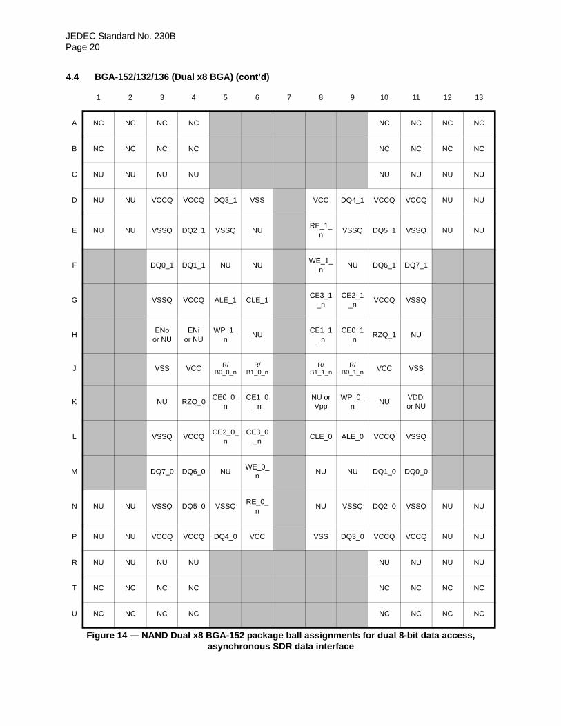
4.4 BGA-152/132/136 (Dual x8 BGA) (cont’d)
Figure 14 — NAND Dual x8 BGA-152 package ball assignments for dual 8-bit data access, asynchronous SDR data interface
1 2 3 4 5 6 7 8 9 10 11 12 13
A NC NC NC NC NC NC NC NC
B NC NC NC NC NC NC NC NC
C NU NU NU NU NU NU NU NU
D NU NU VCCQ VCCQ DQ3_1 VSS VCC DQ4_1 VCCQ VCCQ NU NU
E NU NU VSSQ DQ2_1 VSSQ NURE_1_
nVSSQ DQ5_1 VSSQ NU NU
F DQ0_1 DQ1_1 NU NUWE_1_
nNU DQ6_1 DQ7_1
G VSSQ VCCQ ALE_1 CLE_1CE3_1
_nCE2_1
_nVCCQ VSSQ
HENo
or NUENi
or NUWP_1_
nNU
CE1_1_n
CE0_1_n
RZQ_1 NU
J VSS VCC R/B0_0_n
R/B1_0_n
R/B1_1_n
R/B0_1_n VCC VSS
K NU RZQ_0CE0_0_
nCE1_0
_nNU orVpp
WP_0_n
NUVDDior NU
L VSSQ VCCQCE2_0_
nCE3_0
_nCLE_0 ALE_0 VCCQ VSSQ
M DQ7_0 DQ6_0 NUWE_0_
nNU NU DQ1_0 DQ0_0
N NU NU VSSQ DQ5_0 VSSQRE_0_
nNU VSSQ DQ2_0 VSSQ NU NU
P NU NU VCCQ VCCQ DQ4_0 VCC VSS DQ3_0 VCCQ VCCQ NU NU
R NU NU NU NU NU NU NU NU
T NC NC NC NC NC NC NC NC
U NC NC NC NC NC NC NC NC

JEDEC Standard No. 230BPage 21
4.4 BGA-152/132/136 (Dual x8 BGA) (cont’d)
Figure 15 — NAND Dual x8 BGA-132 package ball assignments for dual 8-bit data access, asynchronous SDR data interface
1 2 3 4 5 6 7 8 9 10 11
A NC NC NC NC NC NC
B NC NC NC NC NC NC
C NU NU NU NU NU NU
D NU VCCQ VCCQ DQ3_1 VSS VCC DQ4_1 VCCQ VCCQ NU
E NU VSSQ DQ2_1 VSSQ NU RE_1_n VSSQ DQ5_1 VSSQ NU
F DQ0_1 DQ1_1 NU NU WE_1_n NU DQ6_1 DQ7_1
G VSSQ VCCQ ALE_1 CLE_1 CE3_1_n CE2_1_n VCCQ VSSQ
HENo
or NUENi
or NUWP_1_n NU CE1_1_n CE0_1_n RZQ_1 NU
J VSS VCC R/B0_0_n R/B1_0_n R/B1_1_n R/B0_1_n VCC VSS
K NU RZQ_0 CE0_0_n CE1_0_nNU or Vpp
WP_0_n NUVDDior NU
L VSSQ VCCQ CE2_0_n CE3_0_n CLE_0 ALE_0 VCCQ VSSQ
M DQ7_0 DQ6_0 NU WE_0_n NU NU DQ1_0 DQ0_0
N NU VSSQ DQ5_0 VSSQ RE_0_n NU VSSQ DQ2_0 VSSQ NU
P NU VCCQ VCCQ DQ4_0 VCC VSS DQ3_0 VCCQ VCCQ NU
R NU NU NU NU NU NU
T NC NC NC NC NC NC
U NC NC NC NC NC NC

JEDEC Standard No. 230BPage 22
4.4 BGA-152/132/136 (Dual x8 BGA) (cont’d)
Figure 16 — NAND Dual x8 BGA-136 package ball assignments for dual 8-bit data access, asynchronous SDR data interface
1 2 3 4 5 6 7 8 9 10 11 12 13
A NC NC NC NC NC NC NC NC
B NU NU NU NU NU NU NU NU
C NU NU VCCQ VCCQ DQ3_1 VSS VCC DQ4_1 VCCQ VCCQ NU NU
D NU NU VSSQ DQ2_1 VSSQ NU RE_1_n VSSQ DQ5_1 VSSQ NU NU
E DQ0_1 DQ1_1 NU NU WE_1_n NU DQ6_1 DQ7_1
F VSSQ VCCQ ALE_1 CLE_1 CE3_1_n CE2_1_n VCCQ VSSQ
GENo
or NUENi
or NUWP_1_n NU CE1_1_n CE0_1_n RZQ_1 NU
H VSS VCC R/B0_0_n R/B1_0_n R/B1_1_n R/B0_1_n VCC VSS
J NU RZQ_0 CE0_0_n CE1_0_nNU or Vpp
WP_0_n NUVDDior NU
K VSSQ VCCQ CE2_0_n CE3_0_n CLE_0 ALE_0 VCCQ VSSQ
L DQ7_0 DQ6_0 NU WE_0_n NU NU DQ1_0 DQ0_0
M NU NU VSSQ DQ5_0 VSSQ RE_0_n NU VSSQ DQ2_0 VSSQ NU NU
N NU NU VCCQ VCCQ DQ4_0 VCC VSS DQ3_0 VCCQ VCCQ NU NU
P NU NU NU NU NU NU NU NU
R NC NC NC NC NC NC NC NC

JEDEC Standard No. 230BPage 23
4.5 BGA-316 (Quad x8 BGA)
Figure 17 to Figure 18 define the ball assignments for devices using NAND Quad x8 BGA for the Toggle DDR or Synchronous DDR data interface. BGA-316 supports up to 32 CEs for the future extendability in terms of the number of die stacks, thus Figure 17 illustrates the standard package with 16 CEs and Figure 18 shows the extended type of the package with 32 CEs.NC balls indicate mechanical support balls with no internal connection. NU balls at four corner areas indicate mechanical support balls with possible internal connection. Therefore NU balls landing pad must be isolated. Any of the support ball locations may or may not be populated with a ball depending upon the NAND Flash Vendor's actual package size. Therefore it's recommended to consider landing pad location for all possible support balls based upon maximum package size allowed in the application.
Figure 17 — NAND Quad x8 BGA- 316 package ball assignments for quad 8-bit data access with up to 16 CE_ns and 4 R/Bs, Toggle DDR or Synchronous DDR data interface
1 2 3 4 5 6 7 8 9 10 11 12 13 14 15 16
A NC NC NC NC NC NC NC NC NC NC NC NC NC NC NC NC
B NC NC NC VCCQ VSS VCCQ VSSVREF
QVCC VSS VCC VSS VCC NC NC NC
C NC NC VSS VCC VSS DQ7_2 DQ7_0 VCCQ VSSENi
or NUENo
or NUVPP NC NC
D NC VCC VSS VSP VSP DQ6_2 DQ6_0 VSS VSS VSS VSS VSS VCC NC
E NC VCCQ VSS VSP VSP DQ5_2 DQ5_0 VSS R/B_2 RZQ_2 VSS VSS RFU NC
F NC VSS VSS VCCQ VSS DQ4_2 DQ4_0 VSS R/B_0 RZQ_0 VSS VSS VSS NC
G NC VCCQ VSS VCC VSSDQS_2
(DQS_2_t)DQS_0
(DQS_0_t)WP_0_n WP_2_n CE1_2_n CE3_2_n VSS VCC NC
H NC VCC VSS VCCQ VSS DQS_2_c DQS_0_c CLE_0 CLE_2 CE1_0_n CE3_0_n VSS RFU NC
J NC VSP VSP VSS DQ3_2 DQ3_0 RE_2_c RE_0_c ALE_2 CE0_2_n CE2_2_n VSS VSS NC
K NC VCCQ VSS VSS DQ2_2 DQ2_0
RE_2_n(RE_2_t)
orW/R_2_n
RE_0_n(RE_0_t)
orW/R_0_n
ALE_0 CE0_0_n CE2_0_n VSS VCC NC
L NC VDDi VREFQ VSP DQ1_2 DQ1_0WE_2_n
orCK_2
WE_0_nor
CK_0DQ0_1 DQ0_3 VSP VSS VCCQ NC
M NC VCCQ VSS VSP DQ0_2 DQ0_0WE_1_n
orCK_1
WE_3_nor
CK_3DQ1_1 DQ1_3 VSP VREFQ VDDi NC
N NC VCC VSS CE2_1_n CE0_1_n ALE_1
RE_1_n(RE_1_t)
orW/R_1_n
RE_3_n(RE_3_t)
orW/R_3_n
DQ2_1 DQ2_3 VSS VSS VCCQ NC
P NC VSS VSS CE2_3_n CE0_3_n ALE_3 RE_1_c RE_3_c DQ3_1 DQ3_3 VSS VSP VSP NC
R NC RFU VSS CE3_1_n CE1_1_n CLE_3 CLE_1 DQS_1_c DQS_3_c VSS VCCQ VSS VCC NC
T NC VCC VSS CE3_3_n CE1_3_n WP_3_n WP_1_nDQS_1
(DQS_1_t)DQS_3
(DQS_3_t)VSS VCC VSS VCCQ NC
U NC VSS VSS VSS RZQ_1 R/B_1 VSS DQ4_1 DQ4_3 VSS VCCQ VSS VSS NC
V NC RFU VSS VSS RZQ_3 R/B_3 VSS DQ5_1 DQ5_3 VSP VSP VSS VCCQ NC
W NC VCC VSS VSS VSS VSS VSS DQ6_1 DQ6_3 VSP VSP VSS VCC NC
Y NC NC VPP RFU RFU VSS VCCQ DQ7_1 DQ7_3 VSS VCC VSS NC NC
AA NC NC NC VCC VSS VCC VSS VCCVREF
QVSS VCCQ VSS VCCQ NC NC NC
AB NC NC NC NC NC NC NC NC NC NC NC NC NC NC NC NC

JEDEC Standard No. 230BPage 24
4.5 BGA-316 (Quad x8 BGA) (cont’d)
Figure 18 — NAND Quad x8 BGA- 316 package ball assignments for quad 8-bit data access with up to 32 CE_ns and 4 R/Bs, Toggle DDR or Synchronous DDR data interface
1 2 3 4 5 6 7 8 9 10 11 12 13 14 15 16
A NC NC NC NC NC NC NC NC NC NC NC NC NC NC NC NC
B NC NC NC VCCQ VSS VCCQ VSSVREF
QVCC VSS VCC VSS VCC NC NC NC
C NC NC VSS VCC VSS DQ7_2 DQ7_0 VCCQ VSSENi
or NUENo
or NUVPP NC NC
D NC VCC VSS VSP VSP DQ6_2 DQ6_0 VSS VSS VSS VSS VSS VCC NC
E NC VCCQ VSS VSP VSP DQ5_2 DQ5_0 VSS R/B0_2 RZQ_2 CE6_2_n CE7_2_n RFU NC
F NC VSS VSS VCCQ VSS DQ4_2 DQ4_0 VSS R/B0_0 RZQ_0 CE6_0_n CE7_0_n VSS NC
G NC VCCQ VSS VCC VSSDQS_2
(DQS_2_t)DQS_0
(DQS_0_t)WP_0_n WP_2_n CE1_2_n CE3_2_n CE5_2_n VCC NC
H NC VCC VSS VCCQ VSS DQS_2_c DQS_0_c CLE_0 CLE_2 CE1_0_n CE3_0_n CE5_0_n RFU NC
J NC VSP VSP VSS DQ3_2 DQ3_0 RE_2_c RE_0_c ALE_2 CE0_2_n CE2_2_n CE4_2_n VSS NC
K NC VCCQ VSS VSS DQ2_2 DQ2_0
RE_2_n(RE_2_t)
or W/R_2_n
RE_0_n(RE_0_t)
or W/R_0_n
ALE_0 CE0_0_n CE2_0_n CE4_0_n VCC NC
L NC VDDi VREFQ VSP DQ1_2 DQ1_0WE_2_n
orCK_2
WE_0_nor
CK_0DQ0_1 DQ0_3 VSP VSS VCCQ NC
M NC VCCQ VSS VSP DQ0_2 DQ0_0WE_1_n
or CK_1
WE_3_nor
CK_3DQ1_1 DQ1_3 VSP VREFQ VDDi NC
N NC VCC CE4_1_n CE2_1_n CE0_1_n ALE_1
RE_1_n(RE_1_t)
orW/R_1_n
RE_3_n(RE_3_t)
or W/R_3_n
DQ2_1 DQ2_3 VSS VSS VCCQ NC
P NC VSS CE4_3_n CE2_3_n CE0_3_n ALE_3 RE_1_c RE_3_c DQ3_1 DQ3_3 VSS VSP VSP NC
R NC RFU CE5_1_n CE3_1_n CE1_1_n CLE_3 CLE_1 DQS_1_c DQS_3_c VSS VCCQ VSS VCC NC
T NC VCC CE5_3_n CE3_3_n CE1_3_n WP_3_n WP_1_nDQS_1
(DQS_1_t)DQS_3
(DQS_3_t)VSS VCC VSS VCCQ NC
U NC VSS CE7_1_n CE6_1_n RZQ_1 R/B0_1 VSS DQ4_1 DQ4_3 VSS VCCQ VSS VSS NC
V NC RFU CE7_1_n CE6_3_n RZQ_3 R/B0_3 VSS DQ5_1 DQ5_3 VSP VSP VSS VCCQ NC
W NC VCC VSS VSS VSS VSS VSS DQ6_1 DQ6_3 VSP VSP VSS VCC NC
Y NC NC VPP RFU RFU VSS VCCQ DQ7_1 DQ7_3 VSS VCC VSS NC NC
AA NC NC NC VCC VSS VCC VSS VCCVREF
QVSS VCCQ VSS VCCQ NC NC NC
AB NC NC NC NC NC NC NC NC NC NC NC NC NC NC NC NC

JEDEC Standard No. 230BPage 25
4.6 BGA-272 (Quad x8 BGA)
Figure 19 defines the ball assignments for devices using NAND Quad x8 BGA for the Toggle DDR or Synchronous DDR data interface. NC balls indicate mechanical support balls with no internal connection. NU balls at four corner areas indicate mechanical support balls with possible internal connection. Therefore NU balls landing pad must be isolated. Any of the support ball locations may or may not be populated with a ball depending upon the NAND Flash Vendor's actual package size. Therefore it's recommended to consider landing pad location for all possible support balls based upon maximum package size allowed in the application.
Figure 19 — NAND Quad x8 BGA- 272 package ball assignments for quad 8-bit data access with up to 16 CE_ns and 4 R/Bs, Toggle DDR or Synchronous DDR data interface
1 2 3 4 5 6 7 8 9 10 11 12 13 14 15 16
A NC NC NC NU NU NC NC NC
B NC NC NU VCCQ VSS VSS VSS VCC VCCQ VSS VCCQ NU NC NC
C NC NU VCCQ VSS VSS DQ0_2 DQ0_0 VSS VSS VSS VSS VCC NU NC
D NU VCC VSS VSS VSS DQ1_2 DQ1_0 DQ4_2 DQ4_0 VSS VSS VSS VCC NU
E NU VCC VSS VSS VSS DQ2_2 DQ2_0 DQ5_2 DQ5_0 VSS VSS VSS VSS NU
F VSS VSS VSS DQ3_0DQS_2
(DQS_2_t)DQS_0
(DQS_0_t)DQ6_2 DQ6_0 VSS VSS VSS VCCQ
G VCCQ VSS VSS DQ3_2 DQS_2_c DQS_0_c VCCQ DQ7_2 DQ7_0 RZQ_2 RZQ_0 VCCQ
H VCCQ VSS VSSVSP0
RVSP2
RVSS
WE_0_nor
CK_0CE1_0_n CE3_0_n R/B0_0_n R/B1_0_n VSS
J ENior NU
ENoor NU
VSS VSS VSS VSSWE_2_n
orCK_2
CE1_2_n CE3_2_n R/B0_2_n R/B1_2_nVSP6
R
K VCC WP_0_n ALE_0 CLE_0
RE_0_n(RE_0_t)
orW/R_0_n
RE_0_c CE0_2_n CE0_0_n CE2_2_n CE2_0_nVSP4
or VDDiVPP
L NU WP_2_n ALE_2 CLE_2
RE_2_n(RE_2_t)
orW/R_2_n
RE_2_c VREFQ VREFQ VSS VSS VSS VSS
M VSS VSS VSS VSS VREFQ VREFQ RE_3_c
RE_3_n(RE_3_t)
orW/R_3_n
CLE_3 ALE_3 WP_3_n NU
N VPPVSP5
or VDDiCE2_1_n CE2_3_n CE0_1_n CE0_3_n RE_1_c
RE_1_n(RE_1_t)
orW/R_1_n
CLE_1 ALE_1 WP_1_n VCC
P VSP7R
R/B1_3_n R/B0_3_n CE3_3_n CE1_3_nWE_3_n
orCK_3
VSS VSS VSS VSS NU NU
R VSS R/B1_1_n R/B0_1_n CE3_1_n CE1_1_nWE_1_n
orCK_1
VSSVSP3
RVSP1
RVSS VSS VCCQ
T VCCQ RZQ_1 RZQ_3 DQ7_1 DQ7_3 VCCQ DQS_1_c DQS_3_c DQ3_3 VSS VSS VCCQ
U VCCQ VSS VSS VSS DQ6_1 DQ6_3DQS_1
(DQS_1_t)DQS_3
(DQS_3_t)DQ3_1 VSS VSS VSS
V NU VSS VSS VSS VSS DQ5_1 DQ5_3 DQ2_1 DQ2_3 VSS VSS VSS VCC NU
W NU VCC VSS VSS VSS DQ4_1 DQ4_3 DQ1_1 DQ1_3 VSS VSS VSS VCC NU
Y NC NU VCC VSS VSS VSS VSS DQ0_1 DQ0_3 VSS VSS VCCQ NU NC
AA NC NC NU VCCQ VSS VCCQ VCC VSS VSS VSS VCCQ NU NC NC
AB NC NC NC NU NU NC NC NC

JEDEC Standard No. 230BPage 26
5 Command Sets for NAND Flash memory
5.1 Basic Command Definition
Table 8 outlines the commands defined for NAND Flash memory.
The value specified in the first command cycle identifies the command to be performed. Some commands have a second command cycle as specified in Table 8. Typically, commands that have a second command cycle include an address.
Table 8 — Command set
Command O/M1st
Cycle2nd
Cycle
Acceptable while
Accessed LUN is Busy
Acceptable while Other LUNs are
Busy
Target level commands
Page Read
Copyback Read
Change Read Column
Read Cache Random
Read Cache Sequential
Read Cache End
Block Erase
Page Program
Copyback Program
Change Write Column
Get Features
Set Features
Page Cache Program
Read Status
Read Unique ID
Reset
Synchronous Reset
Reset LUN
M 00h 30h Y
O 00h 35h Y
M 05h E0h Y
O 00h 31h Y
O 31h na Y
O 3Fh na Y
M 60h D0h Y
M 80h 10h Y
O 85h 10h Y
M 85h na Y
O EEh na Y
O EFh na Y
O 80h 15h Y
M 70h na Y
O EDh na Y
M FFh na Y Y Y
O FCh na Y Y Y
O FAh Y Y

JEDEC Standard No. 230BPage 27
5.2 Primary & Secondary Command Definition For the Advanced Operation
Table 9 defines the Primary and Secondary Commands. Primary commands are the recommended implementation for a particular command. Secondary commands are an alternate implementation approach that is allowed for backwards compatibility. All commands are optional. Commands may be used with any data interface (asynchronous SDR, Toggle DDR, or Synchronous DDR).
Table 9 — Primary and Secondary Commands
Command O/MPrimary or Secondary
1st Cycle 2nd CycleONFI or Toggle-mode Heritage
(remove in future)
Multi-plane Read OPrimary 00h 32h ONFI
Secondary 60h 30h Toggle-mode
Multi-plane Read Cache Random
OPrimary 00h 31h ONFI
Secondary 60h 3Ch Toggle-mode
Multi-plane Copyback Read OPrimary 00h 35h ONFI
Secondary 60h 35h Toggle-mode
Random Data Out OPrimary
00h05h
n/aE0h
Toggle-mode
Secondary 06h E0h ONFI
Multi-plane Program OPrimary 80h or 81h 11h Toggle-mode
Secondary 80h 11h ONFI
Multi-plane Copyback Program OPrimary 85h or 81h 11h Toggle-mode
Secondary 85h 11h ONFI
Multi-plane Block Erase OPrimary 60h n/a Toggle-mode
Secondary 60h D1h ONFI
Read Status Enhanced OPrimary 78h n/a ONFI
Secondary F1h/F2h n/a Toggle-mode
JEDEC Standard No. 230BPage 28
6 Set/Get Feature for each LUN
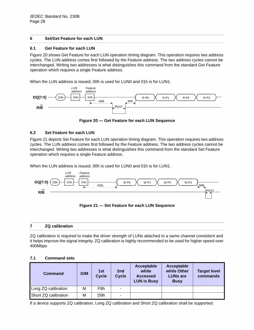
6.1 Get Feature for each LUN
Figure 20 shows Get Feature for each LUN operation timing diagram. This operation requires two address cycles. The LUN address comes first followed by the Feature address. The two address cycles cannot be interchanged. Writing two addresses is what distinguishes this command from the standard Get Feature operation which requires a single Feature address.
When the LUN address is issued, 00h is used for LUN0 and 01h is for LUN1.
Figure 20 — Get Feature for each LUN Sequence
6.2 Set Feature for each LUN
Figure 21 depicts Set Feature for each LUN operation timing diagram. This operation requires two address cycles. The LUN address comes first followed by the Feature address. The two address cycles cannot be interchanged. Writing two addresses is what distinguishes this command from the standard Set Feature operation which requires a single Feature address.
When the LUN address is issued, 00h is used for LUN0 and 01h is for LUN1.
Figure 21 — Set Feature for each LUN Sequence
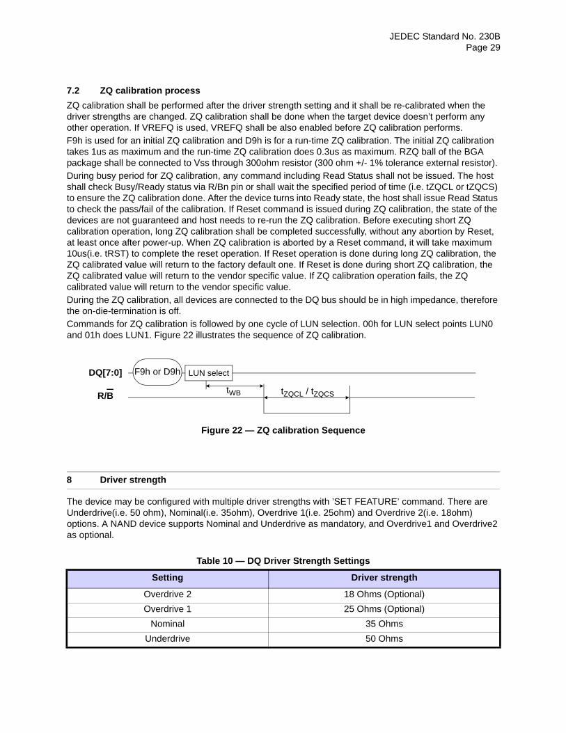
7 ZQ calibration
ZQ calibration is required to make the driver strength of LUNs attached to a same channel consistent and it helps improve the signal integrity. ZQ calibration is highly recommended to be used for higher speed over 400Mbps
7.1 Command sets
If a device supports ZQ calibration, Long ZQ calibration and Short ZQ calibration shall be supported.
Command O/M1st
Cycle2nd
Cycle
Acceptable while
Accessed LUN is Busy
Acceptable while Other LUNs are
Busy
Target level commands
Long ZQ calibration M F9h -
Short ZQ calibration M D9h -
DQ[7:0]
R/B tFEAT
D4h XXh R-P0 R-P1 R-P2 R-P3tWB tRR
XXh
LUN Feature address address
R/B tFEAT
DQ[7:0] D5h XXh W-P1 W-P2 W-P3W-P0tADL tWB
XXh
LUN Feature address address
JEDEC Standard No. 230BPage 29
7.2 ZQ calibration process
ZQ calibration shall be performed after the driver strength setting and it shall be re-calibrated when the driver strengths are changed. ZQ calibration shall be done when the target device doesn’t perform any other operation. If VREFQ is used, VREFQ shall be also enabled before ZQ calibration performs.
F9h is used for an initial ZQ calibration and D9h is for a run-time ZQ calibration. The initial ZQ calibration takes 1us as maximum and the run-time ZQ calibration does 0.3us as maximum. RZQ ball of the BGA package shall be connected to Vss through 300ohm resistor (300 ohm +/- 1% tolerance external resistor).
During busy period for ZQ calibration, any command including Read Status shall not be issued. The host shall check Busy/Ready status via R/Bn pin or shall wait the specified period of time (i.e. tZQCL or tZQCS) to ensure the ZQ calibration done. After the device turns into Ready state, the host shall issue Read Status to check the pass/fail of the calibration. If Reset command is issued during ZQ calibration, the state of the devices are not guaranteed and host needs to re-run the ZQ calibration. Before executing short ZQ calibration operation, long ZQ calibration shall be completed successfully, without any abortion by Reset, at least once after power-up. When ZQ calibration is aborted by a Reset command, it will take maximum 10us(i.e. tRST) to complete the reset operation. If Reset operation is done during long ZQ calibration, the ZQ calibrated value will return to the factory default one. If Reset is done during short ZQ calibration, the ZQ calibrated value will return to the vendor specific value. If ZQ calibration operation fails, the ZQ calibrated value will return to the vendor specific value.
During the ZQ calibration, all devices are connected to the DQ bus should be in high impedance, therefore the on-die-termination is off.
Commands for ZQ calibration is followed by one cycle of LUN selection. 00h for LUN select points LUN0 and 01h does LUN1. Figure 22 illustrates the sequence of ZQ calibration.
Figure 22 — ZQ calibration Sequence
8 Driver strength
The device may be configured with multiple driver strengths with ’SET FEATURE’ command. There are Underdrive(i.e. 50 ohm), Nominal(i.e. 35ohm), Overdrive 1(i.e. 25ohm) and Overdrive 2(i.e. 18ohm) options. A NAND device supports Nominal and Underdrive as mandatory, and Overdrive1 and Overdrive2 as optional.
Table 10 —
Setting Driver strength
DQ Driver Strength Settings
Overdrive 2 18 Ohms (Optional)
Overdrive 1 25 Ohms (Optional)
Nominal 35 Ohms
Underdrive 50 Ohms
DQ[7:0]
R/B tZQCL / tZQCS
F9h or D9h
tWB
LUN select

JEDEC Standard No. 230BPage 30
9 Parameter Page, revision 1
9.1 Parameter Page Data Structure Definition
Parameter page definitions defines the parameter page data structure. For parameters that span multiple bytes, the least significant byte of the parameter corresponds to the first byte.
Values are reported in the parameter page in units of bytes when referring to items related to the size of data access (as in an 8-bit data access device). For example, the target will return how many data bytes are in a page. For a device that supports 16-bit data access, the host is required to convert byte values to word values for its use.
All optional parameters that are not implemented shall be cleared to 0h by the target.
Byte O/M Description
Revision information and features block
0-3 M Parameter page signature Byte 0: “J” (= 4Ah) Byte 1: “E” (= 45h) Byte 2: “S” (= 53h) Byte 3: “D” (= 44h)
4-5 M Revision number 3-15: Reserved (0) 2: 1 = supports parameter page revision 1.0 and standardrevision 1.0 1: 1 = supports vendor specific parameter page 0: Reserved (0)
6-7 M Features supported 9-15 Reserved (0) 8: 1 = supports program page register clear enhancement 7: 1 = supports external Vpp 6: 1 = supports Toggle Mode DDR 5: 1 = supports Synchronous DDR 4: 1 = supports multi-plane read operations 3: 1 = supports multi-plane program and erase operations 2: 1 = supports non-sequential page programming 1: 1 = supports multiple LUN operations 0: 1 = supports 16-bit data bus width
8-10 M Optional commands supported11-23: Reserved (0)10: 1 = supports Synchronous Reset 9: 1 = supports Reset LUN (Primary) 8: 1 = supports Small Data Move 7: 1 = supports Multi-plane Copyback Program (Primary) 6: 1 = supports Random Data Out (Primary) 5: 1 = supports Read Unique ID 4: 1 = supports Copyback 3: 1 = supports Read Status Enhanced (Primary) 2: 1 = supports Get Features and Set Features 1: 1 = supports Read Cache commands 0: 1 = supports Page Cache Program command
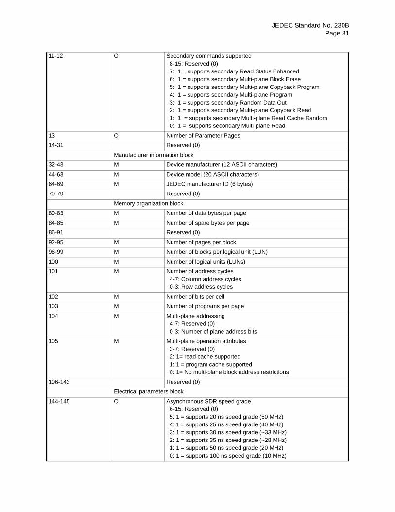
JEDEC Standard No. 230BPage 31
11-12 O Secondary commands supported 8-15: Reserved (0) 7: 1 = supports secondary Read Status Enhanced 6: 1 = supports secondary Multi-plane Block Erase 5: 1 = supports secondary Multi-plane Copyback Program 4: 1 = supports secondary Multi-plane Program 3: 1 = supports secondary Random Data Out 2: 1 = supports secondary Multi-plane Copyback Read 1: 1 = supports secondary Multi-plane Read Cache Random 0: 1 = supports secondary Multi-plane Read
13 O Number of Parameter Pages
14-31 Reserved (0)
Manufacturer information block
32-43 M Device manufacturer (12 ASCII characters)
44-63 M Device model (20 ASCII characters)
64-69 M JEDEC manufacturer ID (6 bytes)
70-79 Reserved (0)
Memory organization block
80-83 M Number of data bytes per page
84-85 M Number of spare bytes per page
86-91 Reserved (0)
92-95 M Number of pages per block
96-99 M Number of blocks per logical unit (LUN)
100 M Number of logical units (LUNs)
101 M Number of address cycles 4-7: Column address cycles 0-3: Row address cycles
102 M Number of bits per cell
103 M Number of programs per page
104 M Multi-plane addressing 4-7: Reserved (0) 0-3: Number of plane address bits
105 M Multi-plane operation attributes 3-7: Reserved (0) 2: 1= read cache supported 1: 1 = program cache supported 0: 1= No multi-plane block address restrictions
106-143 Reserved (0)
Electrical parameters block
144-145 O Asynchronous SDR speed grade 6-15: Reserved (0) 5: 1 = supports 20 ns speed grade (50 MHz) 4: 1 = supports 25 ns speed grade (40 MHz) 3: 1 = supports 30 ns speed grade (~33 MHz) 2: 1 = supports 35 ns speed grade (~28 MHz) 1: 1 = supports 50 ns speed grade (20 MHz) 0: 1 = supports 100 ns speed grade (10 MHz)

JEDEC Standard No. 230BPage 32
146-147 O Toggle Mode DDR and NV-DDR2 speed grade8-15: Reserved (0)7: 1 = supports 5 ns speed grade (200 MHz)6: 1 = supports 6 ns speed grade (~166 MHz)5: 1 = supports 7.5 ns speed grade (~133 MHz)4: 1 = supports 10 ns speed grade (100 MHz)3: 1 = supports 12 ns speed grade (~83 MHz)2: 1 = supports 15 ns speed grade (~66 MHz)1: 1 = supports 25 ns speed grade (40 MHz)0: 1 = supports 30 ns speed grade (~33 MHz)
148-149 O Synchronous DDR speed grade 6-15: Reserved (0) 5: 1 = supports 10 ns speed grade (100 MHz) 4: 1 = supports 12 ns speed grade (~83 MHz) 3: 1 = supports 15 ns speed grade (~66 MHz) 2: 1 = supports 20 ns speed grade (50 MHz) 1: 1 = supports 30 ns speed grade (~33 MHz) 0: 1 = supports 50 ns speed grade (20 MHz)
150 O Asynchronous SDR features 0-7: Reserved (0)
151 O Toggle-mode DDR features 0-7: Reserved (0)
152 O Synchronous DDR features 2-7: Reserved (0) 1: Device supports CK stopped for data input 0: tCAD value to use
153-154 M tPROG Maximum page program time (µs)
155-156 M tBERS Maximum block erase time (µs)
157-158 M tR Maximum page read time (µs)
159-160 O tR Maximum multi-plane page read time (µs)
161-162 O tCCS Minimum change column setup time (ns)
163-164 M I/O pin capacitance, typical
165-166 M Input pin capacitance, typical
167-168 O CK pin capacitance, typical
169 M Driver strength support 3-7: Reserved (0) 2: 1 = supports 18 ohm drive strength 1: 1 = supports 25 ohm drive strength 0: 1 = supports 35ohm/50ohm drive strength
170-171 O tADL Program page register clear enhancement tADL value (ns)
172-207 Reserved (0)
ECC and endurance block
208 M Guaranteed valid blocks at beginning of target
209-210 M Block endurance for guaranteed valid blocks
211-218 M ECC and endurance information block 0 Byte 211: Number of bits ECC correctability Byte 212: Codeword size Byte 213-214: Bad blocks maximum per LUN Byte 215-216: Block endurance Byte 217-218: Reserved (0)

JEDEC Standard No. 230BPage 33
9.2 Byte 0-3: Parameter page signature
This field contains the parameter page signature. When two or more bytes of the signature are valid, then it denotes that a valid copy of the parameter page is present.
Byte 0 shall be set to 4Ah.
Byte 1 shall be set to 45h.
Byte 2 shall be set to 53h.
Byte 3 shall be set to 44h.
9.3 Byte 4-5: Revision number
This field indicates the revisions of the parameter page and standard that the target complies to. The target may support multiple revisions of the standard. This is a bit field where each defined bit corresponds to a particular specification revision that the target may support.
Bit 0 shall be cleared to zero.
Bit 1 when set to one indicates that the target supports vendor specific parameter page.
Bit 2 when set to one indicates that the target supports parameter page rev. 1.0 and standard rev. 1.0.
Bits 3-15 are reserved and shall be cleared to zero.
219-226 O ECC and endurance information block 1 Byte 219: Number of bits ECC correctability Byte 220: Codeword size Byte 221-222: Bad blocks maximum per LUN Byte 223-224: Block endurance Byte 225-226: Reserved (0)
227-234 O ECC and endurance information block 2 Byte 227: Number of bits ECC correctability Byte 228: Codeword size Byte 229-230: Bad blocks maximum per LUN Byte 231-232: Block endurance Byte 233-234: Reserved (0)
235-242 O ECC and endurance information block 3 Byte 235: Number of bits ECC correctability Byte 236: Codeword size Byte 237-238: Bad blocks maximum per LUN Byte 239-240: Block endurance Byte 241-242: Reserved (0)
243-271 Reserved (0)
Reserved
272-419 Reserved (0)
Vendor specific block
420-421 M Vendor specific Revision number
422-509 Vendor specific
CRC for Parameter Page
510-511 M Integrity CRC
Redundant Parameter Pages
512-1023 M Value of bytes 0-511
1024-1535 M Value of bytes 0-511
1536+ Additional redundant parameter pages
JEDEC Standard No. 230BPage 34
9.4 Byte 6-7: Features supported
This field indicates the optional features that the target supports.
Bit 0 when set to one indicates that the target’s data bus width is 16-bits. Bit 0 when cleared to zero indicates that the target’s data bus width is 8-bits. The host shall use the indicated data bus width for all commands that are defined to be transferred at the bus width (x8 or x16). Note that some commands, like Read ID, always transfer data as 8-bit only.
Bit 1 when set to one indicates that the target supports multiple LUN operations. If bit 1 is cleared to zero, then the host shall not issue commands to a LUN unless all other LUNs on the target are idle (i.e. R/B_n is set to one).
Bit 2 when set to one indicates that the target supports non-sequential page programming operations, such that the host may program pages within a block in arbitrary order. Bit 2 when cleared to zero indicates that the target does not support non-sequential page programming operations. If bit 2 is cleared to zero, the host shall program all pages within a block in order starting with page 0.
Bit 3 when set to one indicates that the target supports multi-plane program and erase operations.
Bit 4 when set to one indicates that the target supports multi-plane read operations.
Bit 5 when set to one indicates that the Synchronous DDR data interface is supported by the target. If bit 5 is set to one, then the target shall indicate the Synchronous DDR timing modes supported in the Synchronous DDR timing mode support field. Bit 5 when cleared to zero indicates that the Synchronous DDR data interface is not supported by the target.
Bit 6 when set to one indicates that the Toggle Mode DDR data interface is supported by the target. If bit 6 is set to one, then the target shall indicate the Toggle Mode DDR timing modes supported in the Toggle Mode DDR timing mode support field. Bit 6 when cleared to zero indicates that the Toggle Mode DDR data interface is not supported by the target.
Bit 7 when set to one indicates that the target supports external Vpp. If bit 7 is cleared to zero, then the target does not support external Vpp.
Bit 8 when set to one indicates that the target supports clearing only the page register for the LUN addressed with the Program (80h) command. If bit 8 is cleared to zero, then a Program (80h) command clears the page register for each LUN that is part of the target. At power-on, the device clears the page register for each LUN that is part of the target.
Bits 9-15 are reserved and shall be cleared to zero.

JEDEC Standard No. 230BPage 35
9.5 Byte 8-10: Optional commands supported
This field indicates the optional commands that the target supports.
Bit 0 when set to one indicates that the target supports the Page Cache Program command. If bit 0 is cleared to zero, the host shall not issue the Page Cache Program command to the target.
Bit 1 when set to one indicates that the target supports the Read Cache Random, Read Cache Sequential, and Read Cache End commands. If bit 1 is cleared to zero, the host shall not issue the Read Cache Sequential, Read Cache Random, or Read Cache End commands to the target.
Bit 2 when set to one indicates that the target supports the Get Features and Set Features commands. If bit 2 is cleared to zero, the host shall not issue the Get Features or Set Features commands to the target.
Bit 3 when set to one indicates that the target supports the Read Status Enhanced command. If bit 3 is cleared to zero, the host shall not issue the Read Status Enhanced command to the target. Read Status Enhanced shall be supported if the target has multiple LUNs or supports multi-plane operations.
Bit 4 when set to one indicates that the target supports the Copyback Program and Copyback Read commands. If bit 4 is cleared to zero, the host shall not issue the Copyback Program or Copyback Read commands to the target. If multi-plane operations are supported and this bit is set to one, then multi-plane copyback operations shall be supported.
Bit 5 when set to one indicates that the target supports the Read Unique ID command. If bit 5 is cleared to zero, the host shall not issue the Read Unique ID command to the target.
Bit 6 when set to one indicates that the target supports the Random Data Out command. If bit 6 is cleared to zero, the host shall not issue the Random Data Out command to the target.
Bit 7 when set to one indicates that the target supports the Multi-plane Copyback Program command. If bit 7 is cleared to zero, the host shall not issue the Multi-plane Copyback Program command to the target.
Bit 8 when set to one indicates that the target supports the Small Data Move command for both Program and Copyback operations. If bit 8 is cleared to zero, the target does not support the Small Data Move command for Program or Copyback operations. The Small Data Move command is mutually exclusive with overlapped multi-plane support. When bit 8 is set to one, the device shall support the 11h command to flush any internal data pipeline regardless of whether multi-plane operations are supported.
Bit 9 when set to one indicates that the target supports the Reset LUN command. If bit 9 is cleared to zero, the host shall not issue the Reset LUN command.
Bit 10 when set to one indicates that the target supports the Synchronous Reset command. If bit 10 is cleared to zero, the host shall not issue the Synchronous Reset command.
Bits 11-23 are reserved and shall be cleared to zero.
JEDEC Standard No. 230BPage 36
9.6 Byte 11-12: Secondary commands supported
This field indicates the secondary commands that the target supports.
Bit 0 when set to one indicates that the target supports the secondary Multi-plane Read command. If bit 0 is cleared to zero, the host shall not issue the secondary Multi-plane Read command to the target.
Bit 1 when set to one indicates that the target supports the secondary Multi-plane Read Cache Random command. If bit 1 is cleared to zero, the host shall not issue the secondary Multi-plane Read Cache Random command to the target.
Bit 2 when set to one indicates that the target supports the secondary Multi-plane Copyback Read command. If bit 2 is cleared to zero, the host shall not issue the secondary Multi-plane Copyback Read command to the target.
Bit 3 when set to one indicates that the target supports the secondary Random Data Out command. If bit 3 is cleared to zero, the host shall not issue the secondary Random Data Out command to the target.
Bit 4 when set to one indicates that the target supports the secondary Multi-plane Program command. If bit 4 is cleared to zero, the host shall not issue the secondary Multi-plane Program command to the target.
Bit 5 when set to one indicates that the target supports the secondary Multi-plane Copyback Program command. If bit 5 is cleared to zero, the host shall not issue the secondary Multi-plane Copyback Program command to the target.
Bit 6 when set to one indicates that the target supports the secondary Multi-plane Block Erase command. If bit 6 is cleared to zero, the host shall not issue the secondary Multi-plane Block Erase command to the target.
Bit 7 when set to one indicates that the target supports the secondary Read Status Enhanced command. If bit 7 is cleared to zero, the host shall not issue the secondary Read Status Enhanced command to the target.
Bits 8-15 are reserved and shall be cleared to zero.
9.7 Byte 13: Number of Parameter Pages
This field specifies the number of parameter pages present, including the original and the subsequent redundant versions.
9.8 Byte 14-31 : Reserved (0)
9.9 Byte 32-43: Device manufacturer
This field contains the manufacturer of the device. The content of this field is an ASCII character string of twelve bytes. The device shall pad the character string with spaces (20h), if necessary, to ensure that the string is the proper length.
There is no standard for how the manufacturer represents their name in the ASCII string. If the host requires use of a standard manufacturer ID, it should use the JEDEC manufacturer ID.
JEDEC Standard No. 230BPage 37
9.10 Byte 44-63: Device model
This field contains the model number of the device. The content of this field is an ASCII character string of twenty bytes. The device shall pad the character string with spaces (20h), if necessary, to ensure that the string is the proper length.
9.11 Byte 64-69: JEDEC manufacturer ID
This field contains the JEDEC manufacturer ID for the manufacturer of the device.
9.12 Byte 70-79 : Reserved (0)
9.13 Byte 80-83: Number of data bytes per page
This field contains the number of data bytes per page. The value reported in this field shall be a power of two. The minimum value that shall be reported is 512 bytes.
9.14 Byte 84-85: Number of spare bytes per page
This field contains the number of spare bytes per page. There are no restrictions on the value.
9.15 Byte 86-91 : Reserved (0)
9.16 Byte 92-95: Number of pages per block
This field contains the number of pages per block.
9.17 Byte 96-99: Number of blocks per logical unit
This field contains the number of blocks per logical unit. There are no restrictions on this value.
9.18 Byte 100: Number of logical units (LUNs)
This field indicates the number of logical units the target supports. Logical unit numbers are sequential, beginning with a LUN address of 0. This field shall be greater than zero.
9.19 Byte 101: Number of Address Cycles
This field indicates the number of address cycles used for row and column addresses. The reported number of address cycles shall be used by the host in operations that require row and/or column addresses (e.g., Page Program).
Bits 0-3 indicate the number of address cycles used for the row address. This field shall be greater than zero.
Bits 4-7 indicate the number of address cycles used for the column address. This field shall be greater than zero.
NOTE Throughout this standard examples are shown with 2-byte column addresses and 3-byte row addresses. However, the host is responsible for providing the number of column and row address cycles in each of these sequences based on the values in this field.
9.20 Byte 102: Number of bits per cell
This field indicates the number of bits per cell in the Flash array. This field shall be greater than zero. A value of FFh indicates that the number of bits per cell is not specified.

JEDEC Standard No. 230BPage 38
9.21 Byte 103: Number of programs per page
This field indicates the maximum number of times a portion of a page may be programmed without an erase operation. After the number of programming operations specified have been performed, the host shall issue an erase operation to that block before further program operations to the affected page. This field shall be greater than zero.
9.22 Byte 104: Multi-plane addressing
This field describes parameters for multi-plane addressing.
Bits 0-3 indicate the number of bits that are used for plane addresses. This value shall be greater than 0h when multi-plane operations are supported.
Bits 4-7 are reserved.
9.23 Byte 105: Multi-plane operation attributes
This field describes attributes for multi-plane operations. This byte is mandatory when multi-plane operations are supported as indicated in the Features supported field.
Bit 0 indicates that there are no block address restrictions for the multi-plane operation. If set to one all block address bits may be different between multi-plane operations. If cleared to zero, there are block address restrictions
Bit 1 indicates whether program cache is supported with multi-plane programs. If set to one then program cache is supported for multi-plane program operations. If cleared to zero then program cache is not supported for multi-plane program operations. Note that program cache shall not be used with multi-plane copyback program operations.
Bit 2 indicates whether read cache is supported with multi-plane reads. If set to one then read cache is supported for multi-plane read operations. If cleared to zero then read cache is not supported for multi-plane read operations. Note that read cache shall not be used with multi-plane copyback read operations.
Bits 3-7 are reserved.
9.24 Byte 106-143 : Rserved (0)

JEDEC Standard No. 230BPage 39
9.25 Byte 144-145: Asynchronous SDR speed grade
This field indicates the asynchronous SDR speed grades supported.
Bit 0 when set to one indicates that the target supports the 100 ns speed grade (10 MHz).
Bit 1 when set to one indicates that the target supports the 50 ns speed grade (20 MHz).
Bit 2 when set to one indicates that the target supports the 35 ns speed grade (~28 MHz).
Bit 3 when set to one indicates that the target supports the 30 ns speed grade (~33 MHz).
Bit 4 when set to one indicates that the target supports the 25 ns speed grade (40 MHz).
Bit 5 when set to one indicates that the target supports the 20 ns speed grade (50 MHz).
Bits 6-15 are reserved and shall be cleared to zero.
9.26 Byte 146-147: Toggle-mode DDR and NV-DDR2 speed grade
This field indicates the Toggle-mode DDR and NV-DDR2 speed grades supported. The target shall support an inclusive range of speed grades.
Bit 0 when set to one indicates that the target supports the 30 ns speed grade (~33 MHz).
Bit 1 when set to one indicates that the target supports the 25 ns speed grade (40 MHz).
Bit 2 when set to one indicates that the target supports the 15 ns speed grade (~66 MHz).
Bit 3 when set to one indicates that the target supports the 12 ns speed grade (~83 MHz).
Bit 4 when set to one indicates that the target supports the 10 ns speed grade (100 MHz).
Bit 5 when set to one indicates that the target supports the 7.5 ns speed grade (~133 MHz).
Bit 6 when set to one indicates that the target supports the 6 ns speed grade (~166 MHz).
Bit 7 when set to one indicates that the target supports the 5 ns speed grade (200 MHz).
Bits 8-15 are reserved and shall be cleared to zero.

JEDEC Standard No. 230BPage 40
9.27 Byte 148-149: Synchronous DDR speed grade
This field indicates the synchronous DDR speed grades supported. The target shall support an inclusive range of speed grades.
Bit 0 when set to one indicates that the target supports the 50 ns speed grade (20 MHz).
Bit 1 when set to one indicates that the target supports the 30 ns speed grade (~33 MHz).
Bit 2 when set to one indicates that the target supports the 20 ns speed grade (50 MHz).
Bit 3 when set to one indicates that the target supports the 15 ns speed grade (~66 MHz).
Bit 4 when set to one indicates that the target supports the 12 ns speed grade (~83 MHz).
Bit 5 when set to one indicates that the target supports the 10 ns speed grade (100 MHz).
Bits 6-15 are reserved and shall be cleared to zero.
9.28 Byte 150: Asynchronous SDR features
This field describes features and attributes for asynchronous SDR operation. This byte is mandatory when the asynchronous SDR data interface is supported.
Bits 0-7 are reserved.
9.29 Byte 151: Toggle-mode DDR features
This field describes features and attributes for Toggle-mode DDR operation. This byte is mandatory when the Toggle-mode DDR data interface is supported.
Bits 0-7 are reserved.
9.30 Byte 152: Synchronous DDR features
This field describes features and attributes for synchronous DDR operation. This byte is mandatory when the synchronous DDR data interface is supported.
Bit 0 indicates the tCAD value that shall be used by the host. If bit 0 is set to one, then the host shall use the tCADs (slow) value in synchronous DDR command, address and data transfers. If bit 0 is cleared to zero, then the host shall use the tCADf (fast) value in synchronous DDR command, address and data transfers.
Bit 1 indicates that the device supports the CK being stopped during data input. If bit 1 is set to one, then the host may optionally stop the CK during data input for power savings. If bit 1 is set to one, the host may pause data while the CK is stopped. If bit 1 is cleared to zero, then the host shall leave CK running during data input.
Bits 2-7 are reserved.
9.31 Byte 153-154: Maximum page program time
This field indicates the maximum page program time (tPROG) in microseconds.

JEDEC Standard No. 230BPage 41
9.32 Byte 155-156: Maximum block erase time
This field indicates the maximum block erase time (tBERS) in microseconds.
9.33 Byte 157-158: Maximum page read time
This field indicates the maximum page read time (tR) in microseconds.
9.34 Byte 159-160: Maximum multi-plane page read time
This field indicates the maximum page read time (tR) for multi-plane page reads in microseconds. Multi-plane page read times may be longer than single page read times. This field shall be supported if the target supports multi-plane reads as indicated in the Features supported field.
9.35 Byte 161-162: Minimum change column setup time.
This field indicates the minimum change column setup time (tCCS) in nanoseconds. This parameter is used for the asynchronous SDR and synchronous DDR data interfaces.
After issuing a Change Read Column command, the host shall not read data until a minimum of tCCS time has elapsed. After issuing a Change Write Column command including all column address cycles, the host shall not write data until a minimum of tCCS time has elapsed. The value of tCCS shall always be longer than or equal to tWHR and tADL when the Toggle-mode DDR or Synchronous DDR data interface is supported.
9.36 Byte 163-164: I/O pin capacitance, typical
This field indicates the typical I/O pin capacitance for the target. This field is specified in 0.1 pF units. For example, a value of 31 corresponds to 3.1 pF. The variance from this value is less than +/- 0.5 pF per LUN. As an example, if two LUNs are present than the total variance is less than +/- 1 pF.
9.37 Byte 165-166: Input pin capacitance, typical
This field indicates the typical input pin capacitance for the target. This value applies to all inputs except the following: CK, CK_n, CE_n and WP_n signals. This field is specified in 0.1 pF units. For example, a value of 31 corresponds to 3.1 pF. The variance from this value is less than +/- 0.5 pF per LUN. As an example, if two LUNs are present than the total variance is less than +/- 1 pF.
9.38 Byte 167-168: CK input pin capacitance, typical
This field indicates the typical CK input pin capacitance for the target. This value applies to the CK and CK_n signals. This field is specified in 0.1 pF units. For example, a value of 31 corresponds to 3.1 pF. The variance from this value is less than +/- 0.25 pF per LUN. As an example, if two LUNs are present than the total variance is less than +/- 0.5 pF. This field shall be supported if the Synchronous DDR data interface is supported.

JEDEC Standard No. 230BPage 42
9.39 Byte 169: Driver strength support
This field describes if the target supports configurable driver strengths and its associated features.
Bit 0 when set to one indicates that the target supports configurable driver strength settings as defined in Table 10. If this bit is set to one, then the device shall support both the 35 ohm and 50 ohm settings. If this bit is set to one, then the device shall power-on with a driver strength at the 35 ohm value defined in Table 10. If this bit is cleared to zero, then the driver strength at power-on is undefined. This bit shall be set to one for devices that support the Synchronous DDR or Toggle-mode DDR data interface.
Bit 1 when set to one indicates that the target supports the 25 ohm setting in Table 10 for use in the I/O Drive Strength setting.
Bit 2 when set to one indicates that the target supports the 18 ohm setting in Table 10 for use in the I/O Drive Strength setting.
Bits 3-7 are reserved.
9.40 Byte 170-171: Program page register clear enhancement tADL value
This field indicates the ALE to data loading time (tADL) in nanoseconds when the program page register clear enhancement is enabled. If the program page register clear enhancement is disabled, then the tADL value is as defined for the selected timing mode. This increased tADL value only applies to Program (80h) command sequences; it does not apply for Set Features, Copyback, or other commands.
9.41 Byte 172-207 : Reserved (0)
9.42 Byte 208: Guaranteed valid blocks at beginning of target
This field indicates the number of guaranteed valid blocks starting at block address 0 of the target. The minimum value for this field is 1h. The blocks are guaranteed to be valid for the endurance specified for this area when the host follows the specified number of bits to correct in ECC information block 0.
9.43 Byte 209-210: Block endurance for guaranteed valid blocks
This field indicates the minimum number of program/erase cycles per addressable page/block in the guaranteed valid block area. This value requires that the host is using at least the minimum ECC correctability reported in ECC information block 0. This value is not encoded. If the value is 0000h, then no minimum number of cycles is specified, though the block(s) are guaranteed valid from the factory.

JEDEC Standard No. 230BPage 43
9.44 Byte 211-218: ECC information block 0
This block of parameters describes a set of ECC and endurance information. The parameters are related, and thus the parameters are specified as a set.
Byte 211: Number of bits ECC correctability. This field indicates the number of bits that the host should be able to correct per codeword. The codeword size is reported in byte 212. With this specified amount of error correction by the host, the target shall achieve the block endurance specified in bytes 215-216. When the specified amount of error correction is applied by the host and the block endurance is followed, then the maximum number of bad blocks specified in bytes 213-214 shall not be exceeded by the device. All used bytes in the page shall be protected by ECC including the spare bytes if the ECC requirement reported in byte 211 has a value greater than zero. When this value is cleared to zero, the target shall return valid data.
Byte 212: Codeword size. The number of bits of ECC correctability specified in byte 211 is based on a particular ECC codeword size. The ECC codeword size is specified in this field as a power of two. The minimum value that shall be reported is 512 bytes (a value of 9).
Byte 213-214: Bad blocks maximum per LUN. This field contains the maximum number of blocks that may be defective at manufacture and over the life of the device per LUN. The maximum rating assumes that the host is following the block endurance requirements and the ECC requirements reported in this ECC and endurance information block.
Byte 215-216: Block endurance. This field indicates the maximum number of program/erase cycles per addressable page/block. This value assumes that the host is using the ECC correctability reported in byte 211. The block endurance is reported in terms of a value and a multiplier according to the following equation: value x 10multiplier. Byte 215 comprises the value. Byte 216 comprises the multiplier. For example, a block endurance of 75,000 cycles would be reported as a value of 75 and a multiplier of 3 (75 x 103). The value field shall be the smallest possible; for example 100,000 shall be reported as a value of 1 and a multiplier of 5 (1 x 10⁵). If the value is 0000h, then no maximum number of cycles is specified.
9.45 Byte 219-226: ECC information block 1
This block of parameters describes an additional set of ECC and endurance information. The parameters are related, and thus the parameters are specified as a set. The layout is and definition for this block is equivalent to ECC information block 0. If this set of parameter is not specified, the block shall be cleared to 0h.
9.46 Byte 227-234: ECC information block 2
This block of parameters describes an additional set of ECC and endurance information. The parameters are related, and thus the parameters are specified as a set. The layout is and definition for this block is equivalent to ECC information block 0. If this set of parameter is not specified, the block shall be cleared to 0h.
9.47 Byte 235-242: ECC information block 3
This block of parameters describes an additional set of ECC and endurance information. The parameters are related, and thus the parameters are specified as a set. The layout is and definition for this block is equivalent to ECC information block 0. If this set of parameter is not specified, the block shall be cleared to 0h.
9.48 Byte 243 - 419 : Reserved (0)
JEDEC Standard No. 230BPage 44
9.49 Byte 420-421: Vendor specific Revision number
This field indicates a vendor specific revision number. This field should be used by vendors to indicate the supported layout for the vendor specific parameter page area and the vendor specific feature addresses. The format of this field is vendor specific.
9.50 Byte 422-509: Vendor specific
This field is reserved for vendor specific use.
9.51 Byte 510-511: Integrity CRC
The Integrity CRC (Cyclic Redundancy Check) field is used to verify that the contents of the parameter page were transferred correctly to the host. The CRC of the parameter page is a word (16-bit) field. The CRC calculation covers all of data between byte 0 and byte 509 of the parameter page inclusive.
The CRC shall be calculated on byte (8-bit) quantities starting with byte 0 in the parameter page. The bits in the 8-bit quantity are processed from the most significant bit (bit 7) to the least significant bit (bit 0).
The CRC shall be calculated using the following 16-bit generator polynomial:
G(X) = X16 + X15 + X2 + 1
This polynomial in hex may be represented as 8005h.
The CRC value shall be initialized with a value of 4F4Eh before the calculation begins. There is no XOR applied to the final CRC value after it is calculated. There is no reversal of the data bytes or the CRC calculated value.
9.52 Byte 512-1023: Redundant Parameter Page 1
This field shall contain the values of bytes 0-511 of the parameter page. Byte 512 is the value of byte 0.
The redundant parameter page is used when the integrity CRC indicates that there was an error in bytes 0-511. The redundant parameter page shall be stored in nonvolatile media; the target shall not create these bytes by retransmitting the first 512 bytes.
9.53 Byte 1024-1535: Redundant Parameter Page 2
This field shall contain the values of bytes 0-511 of the parameter page. Byte 1024 is the value of byte 0.
The redundant parameter page is used when the integrity CRC indicates that there was an error in bytes 0-511 and in the first redundant parameter page. The redundant parameter page shall be stored in nonvolatile media; the target shall not create these bytes by retransmitting the first 512 bytes.
9.54 Byte 1536+: Additional Redundant Parameter Pages
Bytes at offset 1536 and above may contain additional redundant copies of the parameter page. There is no limit to the number of redundant parameter pages that the target may provide. The target may provide additional copies to guard against the case where all three mandatory copies have invalid CRC checks.
The host should determine whether an additional parameter page is present by checking the first Dword. If at least two out of four bytes match the parameter page signature, then an additional parameter page is present.

JEDEC Standard No. 230BPage 45
Annex A (informative) Differences between JESD230 and JESD230A
This table briefly describes most of the changes made to entries that appear in this standard,
JESD230B, compared to its predecessor, JESD230A (August 2013). If the change to a concept involves any words added or deleted (excluding deletion of accidentally repeated words), it is included. Some punctuation changes are not included.
Clause Description of change
2 VccQ added
6 ZQ calibration added
7 Driver strength added
8.1.38 Driver strength support description changes in Byte 169 of the parameter page
A.1 Differences between JESD230A and JESD230 (October 2012)
Clause Description of change
2.5 New BGA-316 (Quad x8) package added
2.6 New BGA-272 (Quad x8) package added
5 Parameter page, revision 1 added

JEDEC Standard No. 230BPage 46

Rev. 8/13
Standard Improvement Form JEDEC The purpose of this form is to provide the Technical Committees of JEDEC with input from the industry regarding usage of the subject standard. Individuals or companies are invited to submit comments to JEDEC. All comments will be collected and dispersed to the appropriate committee(s). If you can provide input, please complete this form and return to:
JEDEC Attn: Publications Department 3103 North 10th Street Suite 240 South Arlington, VA 22201-2107
Fax: 703.907.7583
1. I recommend changes to the following:
Requirement, clause number
Test method number Clause number
The referenced clause number has proven to be:
Unclear Too Rigid In Error
Other
2. Recommendations for correction:
3. Other suggestions for document improvement:
Submitted by
Name: Phone:
Company: E-mail:
Address:
City/State/Zip: Date: