JAYA JAYA SANKARA HARA HARA SANKARA Thermal and … · JAYA JAYA SANKARA HARA HARA SANKARA Thermal...
6
JAYA JAYA SANKARA HARA HARA SANKARA Thermal and Power Challenges in High Performance Computing Systems ○Venkat NATARAJAN 1 , PhD., Anand DESHPANDE 1 , PhD., Sudarshan SOLANKI 1 , and Arun CHANDRASEKHAR 2 , Ph.D. 1 Systems Research Center 2 Digital Enterprise Group Intel Technology India Pvt. Ltd. Intel Technology India Pvt. Ltd. Bangalore, 560103, India Bangalore, 560017, India Corresponding Author: Venkat Natarajan, E-mail: [email protected] ABSTRACT This paper provides an overview of the thermal and power challenges in emerging high performance computing platforms. The advent of new sophisticated applications in highly diverse areas such as health, education, finance, entertainment etc. is driving the platform and device requirements for future systems. The key ingredients of future platforms are vertically integrated (3D) die-stacked devices which provide the required performance characteristics with the associated form factor advantages. Two of the major challenges to the design of TSV-based (through-silicon-via) 3D stacked technologies are (i) effective thermal management and (ii) efficient power delivery mechanisms. Some of the key challenges that are articulated in this paper include hot-spot superposition and intensification in a 3D stack, design/optimization of TTSVs (Thermal Through Silicon Vias), non-uniform power loading of multi-die stacks, efficient on-chip power delivery, minimization of electrical hotspots etc. 1. INTRODUCTION Emerging trends in processor technology has led to the rapid development of highly advanced and powerful computers with capabilities that far surpass those of current machines. At the very centre of these high performance computers are multi-core processors which have anywhere between tens to hundreds of computational cores in the silicon. This is a phenomenal leap forward in the computational performance of the processor from those of existing products which offer approximately 4-8 cores in the silicon. This giant leap in performance is driven by a number of emerging software applications such as real-time data mining, artificial intelligence, turbulence modeling, genetic engineering etc. High performance computing, also known as Terascale Computing, has made it possible to generate, process, investigate and create large amounts of data for all kinds of diverse applications. The current paper describes the different challenges and research opportunities in the field of high performance computing. As evidenced by Moore’s law, transistor feature sizes are continually reducing at about 0.7X in linear dimensions per generation which enables a 2X increase in transistor density. This enables the number of transistors in a piece of silicon to exceed beyond 10 billion for the same footprint. Lithography has thus made it possible for the industry to create chips with many cores that can execute several thousand tasks in parallel. Some of the future terascale applications include advanced modeling of fluid physics (wave modeling), advanced gaming systems (virtual reality), real-time data mining, real-time financial model analysis/development, computer vision and personal entertainment systems such as video karaoke. All these applications require high performance, high bandwidth and high computational power. 2. 3D STACKING TECHNOLOGY - KEY INGREDIENT OF FUTURE HIGH PERFORMANCE COMPUTING PLATFORMS The key physical computational ingredients of HPC platforms are vertically stacked device technologies (also known as 3D stacked devices). Herein the devices are stacked on atop the other either as package stacking or die-stacking (Figure 1). Stacking offers tremendous performance advantages in the same volumetric space as a single chip scale package. Figure 1 Die Stacking Technology Figure 2 3D Die Stack Physical Layering DIE 1 DIE 2 DIE 3 DIE 4 INTEGRATED HEAT SPREADER (IHS) ENCAPSULATION DIE-T0-DIE VIAS ILNTERLAYER DIELECTRIC (ILD) C4 BUMPS UNDERFILL THROUGH SILICON VIAS (TSV) Package TIM M CPU DRAM Through-Silicon 1st International Symposium on Thermal Design and Thermophysical Property for Electronics, June 18-20, 2008, Tsukuba
Transcript of JAYA JAYA SANKARA HARA HARA SANKARA Thermal and … · JAYA JAYA SANKARA HARA HARA SANKARA Thermal...
JAYA JAYA SANKARA HARA HARA SANKARA
Thermal and Power Challenges in High Performance Computing Systems
○Venkat NATARAJAN1, PhD., Anand DESHPANDE1, PhD., Sudarshan SOLANKI1, and Arun CHANDRASEKHAR2, Ph.D.
1Systems Research Center 2Digital Enterprise Group
Intel Technology India Pvt. Ltd. Intel Technology India Pvt. Ltd.
Bangalore, 560103, India Bangalore, 560017, India
Corresponding Author: Venkat Natarajan, E-mail: [email protected]
ABSTRACT
This paper provides an overview of the thermal and power challenges in emerging high performance computing platforms. The advent of new
sophisticated applications in highly diverse areas such as health, education, finance, entertainment etc. is driving the platform and device
requirements for future systems. The key ingredients of future platforms are vertically integrated (3D) die-stacked devices which provide the
required performance characteristics with the associated form factor advantages. Two of the major challenges to the design of TSV-based
(through-silicon-via) 3D stacked technologies are (i) effective thermal management and (ii) efficient power delivery mechanisms. Some of the
key challenges that are articulated in this paper include hot-spot superposition and intensification in a 3D stack, design/optimization of TTSVs
(Thermal Through Silicon Vias), non-uniform power loading of multi-die stacks, efficient on-chip power delivery, minimization of electrical
hotspots etc.
1. INTRODUCTION Emerging trends in processor technology has led to the rapid
development of highly advanced and powerful computers with
capabilities that far surpass those of current machines. At the very
centre of these high performance computers are multi-core
processors which have anywhere between tens to hundreds of
computational cores in the silicon. This is a phenomenal leap
forward in the computational performance of the processor from
those of existing products which offer approximately 4-8 cores in
the silicon. This giant leap in performance is driven by a number of
emerging software applications such as real-time data mining,
artificial intelligence, turbulence modeling, genetic engineering etc.
High performance computing, also known as Terascale Computing,
has made it possible to generate, process, investigate and create
large amounts of data for all kinds of diverse applications. The
current paper describes the different challenges and research
opportunities in the field of high performance computing.
As evidenced by Moore’s law, transistor feature sizes are
continually reducing at about 0.7X in linear dimensions per
generation which enables a 2X increase in transistor density. This
enables the number of transistors in a piece of silicon to exceed
beyond 10 billion for the same footprint. Lithography has thus
made it possible for the industry to create chips with many cores
that can execute several thousand tasks in parallel.
Some of the future terascale applications include advanced
modeling of fluid physics (wave modeling), advanced gaming
systems (virtual reality), real-time data mining, real-time financial
model analysis/development, computer vision and personal
entertainment systems such as video karaoke. All these
applications require high performance, high bandwidth and high
computational power.
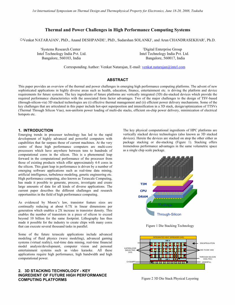
2. 3D STACKING TECHNOLOGY - KEY INGREDIENT OF FUTURE HIGH PERFORMANCE COMPUTING PLATFORMS
The key physical computational ingredients of HPC platforms are
vertically stacked device technologies (also known as 3D stacked
devices). Herein the devices are stacked on atop the other either as
package stacking or die-stacking (Figure 1). Stacking offers
tremendous performance advantages in the same volumetric space
as a single chip scale package.
Figure 1 Die Stacking Technology
Figure 2 3D Die Stack Physical Layering
SUBSRATE
DIE 1
DIE 2
DIE 3
DIE 4
INTEGRATED HEAT SPREADER (IHS)
ENCAPSULATION
DIE-T0-DIE VIAS ILNTERLAYER DIELECTRIC
(ILD)
C4 BUMPS UNDERFILL
THROUGH SILICON VIAS (TSV)
Package
TIM
M
CPU
DRAM
Through-Silicon
1st International Symposium on Thermal Design and Thermophysical Property for Electronics, June 18-20, 2008, Tsukuba
In the case of wire-bonded and package stacks, the process of
manufacturing stacked devices is mature and reliable. The big
challenge in the industry today is that of developing Through-
Silicon-Via (TSV)-based stacking technologies. In this technology,
the through vias are created through the different dies that are
stacked. These through-vias are used as interconnects for signal,
power and thermal reasons. Figure 2 schematically shows a die-
stack with TSVs.
Stacked packages are finding applications in the entire spectrum of
platforms: from high-end servers to commercial desktops to
mobility products. Common applications of stacked packages
include high performance memory including DRAM and flash
memory, logic-memory stack, system in a package or SIP etc. For
example, memory modules with stacked packages are becoming
necessary due to the very high bandwidth as well as latency
requirements. Integrated logic and memory (often vertically
stacked) are often used in applications such as cell-phones and
small form factor devices. Ultra-high workloads for servers, on the
other hand, are beginning to demand extraordinary memory and
computational performance and it appears that this can be met only
through stacking of packages. While there is a significant amount
of research work that has been done on single chip scale packages,
a similar body of work needs to be performed on stacked packages.
Because of the rapid evolution of the platforms with their shrinking
footprints, the power densities of the packages are reaching
extraordinary levels and the associated cooling requirements have
become extremely significant. On the other hand, the cost
constraints are constantly on the downward ramp and the industry
continually strives for innovative means to employ air cooling even
for higher power applications.
3. HEAT TRANSFER RESEARCH ON STACKED DEVICES – A BRIEF SUMMARY Heat transfer research on single chip electronic packages has been
ongoing for over two decades and a phenomenal amount of data
and work can be found in the open literature. Since the amount of
research is enormous, only some of the key research that is relevant
to the present study is mentioned here. Wirtz [1] provides an
excellent review of convective cooling on electronic packages.
Sparrow et al. [2, 3] investigated heat transfer enhancement in
package arrays and also examined effect of flow bypass on the
package heat transfer. Anderson and Moffat [4] examined arrays of
electronic packages to understand the effects of turbulence on the
element heat transfer. Chyu and Natarajan [5, 6] have done a
significant amount of work on forced convective cooling of solitary
cubical elements and developed correlations for both local and
average heat transfer. The Reynolds number dependencies for the
average heat transfer from solitary un-stacked electronic packages
are consistent with the findings of Igarashi [7, 8] and Goldstein [9]
on two dimensional flow regimes around a tall cylinder/prism.
There are several other studies that have focused on single chip
package heat transfer and are too numerous to mention in this paper.
The thermal performance of three-dimensional multi-chip modules
in free convection is examined using both computational and
experimental methods by Chen et. al. [10]. The development of
advanced thermal resistance models for stacked packages is the
focus of the work done by Im and Banerjee [11]. There is a major
effort to investigate 3-D stacking thermal phenomena by Agonafer
et al. and in their recent work [12], the reliability of stacked
packages and associate thermal issues are studied. An interesting
study of the application of pulsating heat pipes to three-
dimensional stacked electronic modules is performed by
Khandekar et al. [13]. Substrate enhancement techniques have been
looked at by Sienski et al. [14]. Recently, there was a detailed
analysis of the thermal characteristics of a stacked electronic
package (P-O-P) by Natarajan [15]. In this work, rules of
estimation were developed for different P-O-P and die-stacked
configurations.
4. THERMAL CHALLENGES IN 3D STACKED DEVICES As stated earlier, there is a lack of a comprehensive description of
the thermal challenges for 3D stacked device technology and it is
the purpose of this current paper to alleviate that need. The thermal
design of a stacked package is very complex and often requires
elaborate models and analyses with large design times. A number
of fundamental questions pertaining to forced convective cooling
of stacked packages need to be addressed. Some of these questions
include: how does the thermal performance vary between stacked
and single chip packages? What is the flow dependency of stack
heat transfer and does it demonstrate the same behavior as those of
single chip devices? What is the effect of board conduction on the
heat transfer from the different dies of a stacked package? Is there
any scalability of the heat transfer data of a single chip package to
that of a multi-chip stack? What are the thermo-mechanical
challenges (such as TSV stress characteristics, fatigue behavior,
effect of thermal cycling) of stacked devices? What are the
optimization implications of TTSVs floorplanning to maximize
heat flow from the stack and minimize the die temperature? What
is the effect of non-uniform power dissipation (power-map) of the
different dies on the cooling requirements of the stacked package?
This section describes some of the key thermal challenges in 3D
stacked devices:
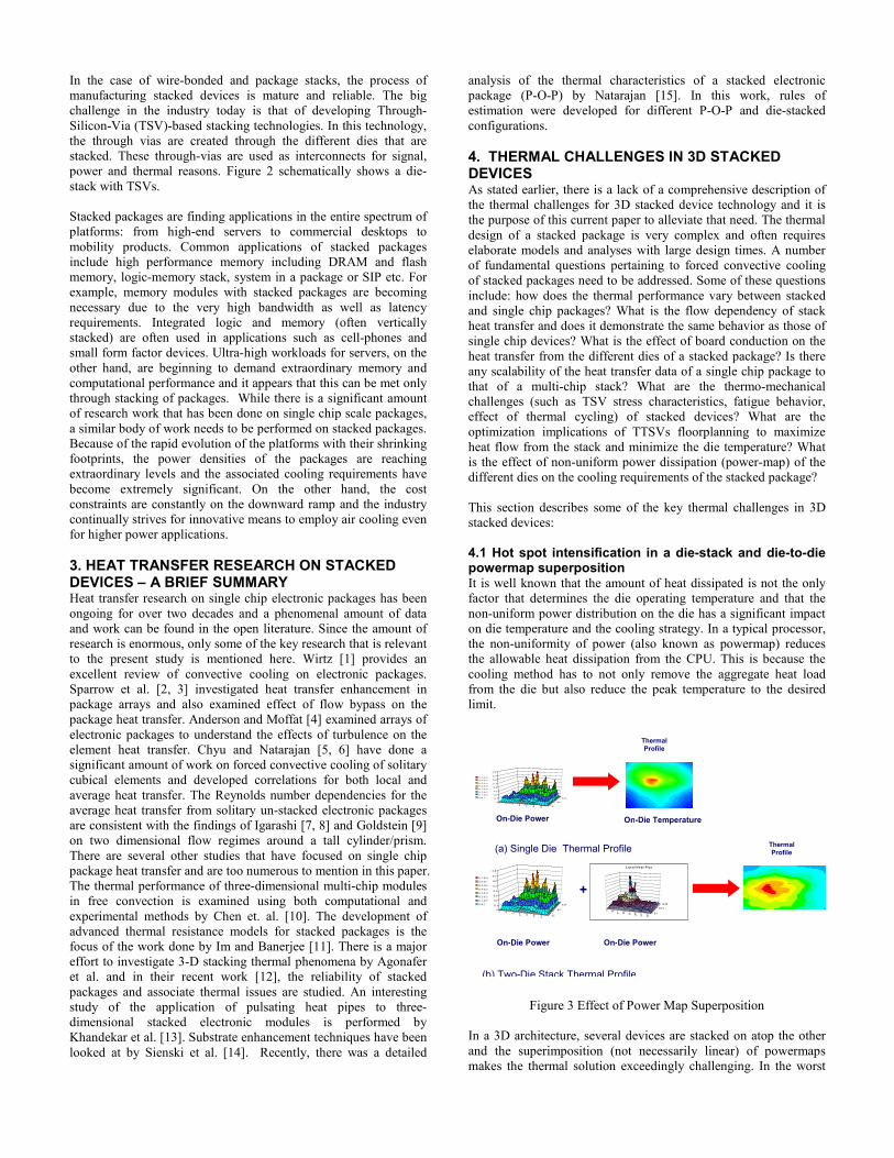
4.1 Hot spot intensification in a die-stack and die-to-die powermap superposition It is well known that the amount of heat dissipated is not the only
factor that determines the die operating temperature and that the
non-uniform power distribution on the die has a significant impact
on die temperature and the cooling strategy. In a typical processor,
the non-uniformity of power (also known as powermap) reduces
the allowable heat dissipation from the CPU. This is because the
cooling method has to not only remove the aggregate heat load
from the die but also reduce the peak temperature to the desired
limit.
Figure 3 Effect of Power Map Superposition
In a 3D architecture, several devices are stacked on atop the other
and the superimposition (not necessarily linear) of powermaps
makes the thermal solution exceedingly challenging. In the worst
1 4 7
10
13
16
19 S1
S9
S17
0
0.1
0.2
0.3
0.4
0.5
0.6
0.7
0.8
0.7-0.8
0.6-0.7
0.5-0.6
0.4-0.5
0.3-0.4
0.2-0.3
0.1-0.2
0-0.1
On-Die Temperature Map
On-Die Power Map
Thermal
Profile
1 4 7
10
13
16
19 S1
S9
S17
0
0.1
0.2
0.3
0.4
0.5
0.6
0.7
0.8
0.7-0.8
0.6-0.7
0.5-0.6
0.4-0.5
0.3-0.4
0.2-0.3
0.1-0.2
0-0.1
On-Die Power Map
1 6
11
16
21
26
31
36
S 1
S 15
S 29
Loc al H e at F lux
+
On-Die Power Map
(b) Two-Die Stack Thermal Profile
(a) Single Die Thermal Profile Thermal
Profile
case, if the active regions or hot spots on each of the dies are
arranged vertically one on top of the other, the effective power
density rises several-fold giving rise to very high and impractical
operating temperatures. Moreover, the interior dies are further
away from the cooling interface and consequently are harder to
cool. If the cooling is insufficient, then the dies that are on the
interior can have a “thermal runaway” effect causing the system to
freeze up or in an extreme situation, there is thermal breakdown of
the device Figure 3 shows the effect of stacking a second die on top
of a single die. The stacking of the second die creates a thermal
profile that is much worse than in the case without stacking.
4.2. Inner die cooling in a die-stack In a vertically integrated stack of dies or packages, the thermal
resistance to cool the interior dies is high due to the presence of a
number of interfaces between the die and the cooling solution. To
cool a stack, there are essentially two paths for the heat to be
transferred from the interior dies; one, vertically upwards to the
main thermal solution, second, downwards through the package or
motherboard. In a typical CPU package, heat transfer through the
base of the package in usually insignificant. However, in low
power CSPs such as package-stacks (P-O-P), these effects are
significant.
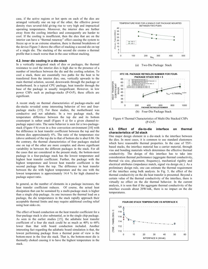
A recent study on thermal characteristics of package-stacks and
die-stacks revealed some interesting behavior of two and four-
package stacks [15]. For these studies, the motherboard was
conductive and not adiabatic. In a two package stack, the
temperature difference between the top die and its bottom
counterpart is rather small (Figure 4 a) for a given channel-to-
package aspect ratio. The same behavior is seen for a two-package-
stack (Figure 4 b) even in a free convection environment [10] with
the difference in heat transfer coefficient between the top and the
bottom dies approximately 6%. The ratio of the temperature rise
(above ambient) of the top die to that of bottom die is abut 0.86. On
the contrary, the thermal characteristics of four packages stacked
one on top of the other are more complex and shows significant
variability in between the different packages in the stack. For all
the cases that are considered in the present study, the bottom-most
package in a four-package stack has the lowest temperature and
highest heat transfer coefficient. Further, the package with the
highest temperature and lowest heat transfer coefficient is the
second package from the top. The difference in heat transfer
between the die with highest temperature and the one with the
lowest temperature is approximately 14.4 % for high channel-to-
package aspect ratio.
In general, as the number of elements in a package increases, the
heat transfer coefficient reduces. Of course, the actual heat
dissipation that can be sustained by a multi-package stack is higher
than a single chip package. As one increases the thermal load on a
package, the die temperatures in the stack rapidly approach their
acceptable thermal limits and may require additional cooling relief
using heat sinks etc.
The effect of board conduction on the heat transfer coefficient for a
four-package stack is also substantial, as in the single chip package.
As seen in the earlier studies [15], the adiabatic heat transfer
coefficient of a four die stack could be as much as 40% to 60%
lower than that with board conduction included. Another
interesting fact regarding the adiabatic board simulation is that, the
lowest performing package from a thermal point of view is the
bottom-most in the four die stack. That is, the bottom-most die is
thermally choked causing it to have the highest temperature in the
stack.
TEMPERATURE RISE FOR A SINGLE CHIP PACKAGE MOUNTED
BETWEEN TWO PCB'S
0
5
10
15
20
25
30
35
40
0 100 200 300 400 500ReB
(TDIE,MAX - TAMBIENT ) DEG.C
W/B = 9
W/B = 1
(a) Two-Die Package Stack
HTC VS. PACKAGE REYNOLDS NUMBER FOR FOUR-
PACKAGE STACK W/B = 5
have = 8.7465ReB0.2934
30
35
40
45
50
55
60
65
0 200 400 600 800 1000PACKAGE REYNOLDS NUMBER
HEAT TRANSFER
COEFFICIENT
W/m2K
BOTTOM PACKAGE W/B = 5SECOND PACKAGE FROM BOTTOM W/B = 5SECOND FROM TOP W/B = 5TOPMOST PACKAGE IN STACK W/B = 5AVERAGE HTC W/B = 5Pow er (AVERAGE HTC W/B = 5)Pow er (AVERAGE HTC W/B = 5)
(b) Four-Die Package Stack
Figure 4 Thermal Characteristics of Multi-Die Stacked CSPs
(P-O-P)
4.3. Effect of die-to-die interface on thermal characteristics of 3d stack One major design element in a die-stack is the interface between
the dies. In most cases, it is common to use standard elastomers
which have reasonable thermal properties. In the case of TSV-
based stacks, the interface material has a carrier material, through
vias and bonding materials which determines the effective thermal
conductivity. The design of this interface has to take into
consideration thermal performance (aggregate thermal conductivity,
thermal via size, placement, frequency), mechanical rigidity and
electrical attributes (impedance match, signal via design etc.). As a
preliminary design rule, one can estimate the thermal requirement
of the interface using bulk analysis. In Fig. 5, the effect of the
thermal conductivity on the die heat transfer is presented. Beyond a
certain value of the thermal conductivity of the interface, there is
virtually no effect on the die thermal behavior. In the current
analysis, it is seen that if the aggregate thermal conductivity of the
interface exceeds about 20W/mK, there is no impact on the die
temperatures.
FOUR-DIE STACK TEMPERATURE VS INTERFACE K
110
112
114
116
118
120
0 10 20 30 40 50 60
INTERFACE K (W/mK)
(TDIE - TAMB) DEG. C
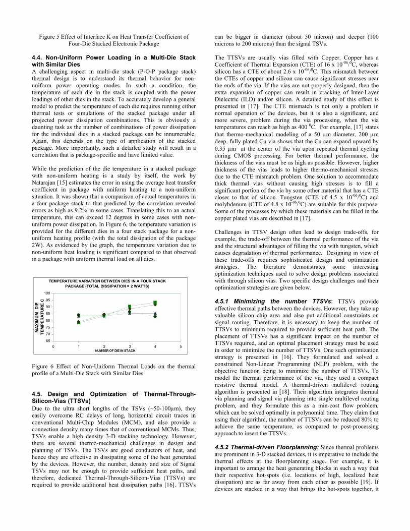
Figure 5 Effect of Interface K on Heat Transfer Coefficient of
Four-Die Stacked Electronic Package
4.4. Non-Uniform Power Loading in a Multi-Die Stack with Similar Dies A challenging aspect in multi-die stack (P-O-P package stack)
thermal design is to understand its thermal behavior for non-
uniform power operating modes. In such a condition, the
temperature of each die in the stack is coupled with the power
loadings of other dies in the stack. To accurately develop a general
model to predict the temperature of each die requires running either
thermal tests or simulations of the stacked package under all
projected power dissipation combinations. This is obviously a
daunting task as the number of combinations of power dissipation
for the individual dies in a stacked package can be innumerable.
Again, this depends on the type of application of the stacked
package. More importantly, such a detailed study will result in a
correlation that is package-specific and have limited value.
While the prediction of the die temperature in a stacked package
with non-uniform heating is a study by itself, the work by
Natarajan [15] estimates the error in using the average heat transfer
coefficient in package with uniform heating to a non-uniform
situation. It was shown that a comparison of actual temperatures in
a four package stack to that predicted by the correlation revealed
errors as high as 9.2% in some cases. Translating this to an actual
temperature, this can exceed 12 degrees in some cases with non-
uniform power dissipation. In Figure 6, the temperature variation is
provided for the different dies in a four stack package for a non-
uniform heating profile (with the total dissipation of the package
2W). As evidenced by the graph, the temperature variation due to
non-uniform heat loading is significant compared to that observed
in a package with uniform thermal load on all dies.
TEMPERATURE VARIATION BETWEEN DIES IN A FOUR STACK
PACKAGE (TOTAL DISSIPATION = 2 WATTS)
65
70
75
80
85
90
95
100
0 1 2 3 4 5NUMBER OF DIE IN STACK
MA
XIM
UM
D
IE
TEM
PER
ATU
RE C
Figure 6 Effect of Non-Uniform Thermal Loads on the thermal
profile of a Multi-Die Stack with Similar Dies
4.5. Design and Optimization of Thermal-Through-Silicon-Vias (TTSVs)
Due to the ultra short lengths of the TSVs (~50-100µm), they
easily overcome RC delays of long, horizontal circuit traces in
conventional Multi-Chip Modules (MCM), and also provide a
connection density many times that of conventional MCMs. Thus,
TSVs enable a high density 3-D stacking technology. However,
there are several thermo-mechanical challenges in design and
planning of TSVs. The TSVs are good conductors of heat, and
hence they are effective in dissipating some of the heat generated
by the devices. However, the number, density and size of Signal
TSVs may not be enough to provide sufficient heat paths, and
therefore, dedicated Thermal-Through-Silicon-Vias (TTSVs) are
required to provide additional heat dissipation paths [16]. TTSVs
can be bigger in diameter (about 50 micron) and deeper (100
microns to 200 microns) than the signal TSVs.
The TTSVs are usually vias filled with Copper. Copper has a
Coefficient of Thermal Expansion (CTE) of 16 x 10-06/0C, whereas
silicon has a CTE of about 2.6 x 10-06/0C. This mismatch between
the CTEs of copper and silicon can cause significant stresses near
the ends of the via. If the vias are not properly designed, then the
extra expansion of copper can result in cracking of Inter-Layer
Dielectric (ILD) and/or silicon. A detailed study of this effect is
presented in [17]. The CTE mismatch is not only a problem in
normal operation of the devices, but it is also a significant, and
more severe, problem during the via processing, when the via
temperatures can reach as high as 400 0C. For example, [17] states
that thermo-mechanical modeling of a 50 µm diameter, 200 µm
deep, fully plated Cu via shows that the Cu can expand upward by
0.35 µm at the center of the via upon repeated thermal cycling
during CMOS processing. For better thermal performance, the
thickness of the vias must be as high as possible. However, higher
thickness of the vias leads to higher thermo-mechanical stresses
due to the CTE mismatch problem. One solution to accommodate
thick thermal vias without causing high stresses is to fill a
significant portion of the via by some other material that has a CTE
closer to that of silicon. Tungsten (CTE of 4.5 x 10-06/0C) and
molybdenum (CTE of 4.8 x 10-06/0C) are suitable for this purpose.
Some of the processes by which these materials can be filled in the
copper plated vias are described in [17].
Challenges in TTSV design often lead to design trade-offs, for
example, the trade-off between the thermal performance of the via
and the structural advantages of filling the via with tungsten, which
causes degradation of thermal performance. Designing in view of
these trade-offs requires sophisticated design and optimization
strategies. The literature demonstrates some interesting
optimization techniques used to solve design problems associated
with through silicon vias. Two specific design challenges and their
optimization strategies are given below.
4.5.1 Minimizing the number TTSVs: TTSVs provide
effective thermal paths between the devices. However, they take up
valuable silicon chip area and also put additional constraints on
signal routing. Therefore, it is necessary to keep the number of
TTSVs to minimum required to provide sufficient heat path. The
placement of TTSVs has a significant impact on the number of
TTSVs required, and an optimal placement strategy must be used
in order to minimize the number of TTSVs. One such optimization
strategy is presented in [16]. They formulated and solved a
constrained Non-Linear Programming (NLP) problem, with the
objective function being to minimize the number of TTSVs. To
model the thermal performance of the via, they used a compact
resistive thermal model. A thermal-driven multilevel routing
algorithm is presented in [18]. Their algorithm integrates thermal
via planning and signal via planning into single multilevel routing
problem, and they formulate this as a min-cost flow problem,
which can be solved optimally in polynomial time. They claim that
using their algorithm, the number of TTSVs can be reduced 80% to
achieve the same temperature, as compared to post-processing
approach to insert the TTSVs.
4.5.2 Thermal-driven Floorplanning: Since thermal problems
are prominent in 3-D stacked devices, it is imperative to include the
thermal effects at the floorplanning stage. For example, it is
important to arrange the heat generating blocks in such a way that
their respective hot-spots (i.e. locations of high, localized heat
dissipation) are as far away from each other as possible [19]. If
devices are stacked in a way that brings the hot-spots together, it
can have severe effect on the maximum temperature, which can
increase beyond an acceptable limit. A thermal-driven
floorplanning algorithm is presented by Cong et. Al [20]. They
developed a new 3-D floorplan representation scheme and used
simulated annealing for optimization. They integrated a compact
resistive thermal model with the 3-D floorplanning algorithm.
Another algorithm for efficient thermal placement of devices is
presented in [21]. This algorithm uses a forced-directed iterative
scheme, in which thermal forces drive cells away from areas of
high temperature. They use finite element analysis to calculate
temperatures in each iteration.
4.6 Multi-disciplinary Optimization (MDO) The design challenges described in the paper involve various
disciplines such as thermal, mechanical and electrical aspects. The
solutions exhibit inherent trade-offs between these disciplines. For
example, as described earlier, thicker TTSVs completely filled with
copper offer excellent thermal paths and help in minimizing the
peak die temperatures. However, they result in severe stresses due
to thermal expansion mismatch, and to mitigate these stresses, the
TTSvs are often filled with tungsten. This results in a decrease in
the TTSV performance as a thermal path, but increases the
reliability. Another case of the inherent trade-off between
disciplines is present in the die stacking design. If the dies are
stacked in such a way that their “active cells” are aligned on top of
each other, this reduces the total wire length (which is essential to
minimize the signal delays). However, this results in hot spot
alignment and causes “thermal runaway” problems as described
earlier. If the hot spots are kept away from each other to minimize
the peak temperature, then it causes an increase in the wire length.
Sophisticated Multi-Disciplinary Optimization (MDO) techniques
are required to solve these problems. Development of the MDO
techniques, development of “fast physics” models and other
techniques to increase the efficiency of the optimization algorithms
is an active area of research in the scientific community worldwide.
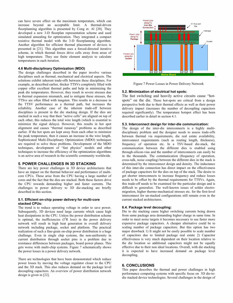
5. POWER CHALLENGES IN 3D STACKING There are key power challenges in 3D device architectures that
have an impact on the thermal behavior and performance of multi-
core CPUs. These arise from the CPU having a large number of
cores and the fact that the dies are stacked. Both these factors drive
the CPU towards demanding higher and faster currents. The
challenges in power delivery to 3D die-stacking are briefly
described in this section.
5.1. Efficient on-chip power delivery for multi-core stacked CPUs: The trend is to reduce operating voltage in order to save power.
Subsequently, 3D devices need large currents which cause high
heat dissipations in the CPU. Unless the power distribution scheme
is optimal, the inefficiencies (I2R loss) in the power delivery
network will result in high heat generation in overall delivery
network including package, socket and platform. The practical
realization of such a fine-grain on-chip power distribution is a huge
challenge. Even in single chip systems, the non-uniformity in
current distribution through socket pins is a problem due to
resistance differences between packages, board power planes. This
gets worse with multi-chip systems. Figure 7 schematically shows
the power losses in a power delivery network.
There are technologies that have been demonstrated which reduce
power losses by moving the voltage regulator closer to the CPU
and the 3D stack. This also reduces demand on the package level
decoupling capacitors. An overview of power distribution network
design is given in [22].
.
Figure 7 Power Losses in Power Delivery Network
5.2. Minimization of electrical hot spots:
The fast switching and heavily active circuits cause “hot-
spots” on the die. These hot-spots are critical from a design
perspective both due to their thermal effects as well as their power
delivery impact (increases the number of decoupling capacitors
required significantly). The temperature hotspot effect has been
described earlier in detail in section 4.1.
5.3. Interconnect design for inter-die communication: The design of the inter-die interconnects is a highly multi-
disciplinary problem and the designer needs to assess trade-offs
between thermal via requirements, die real estate availability,
interconnect requirements (such as routing length, thickness),
frequency of operation etc. In a TSV-based die-stack, the
communication between the different dies is enabled using
through-silicon-vias and the number of interconnects can easily be
in the thousands. The communication (frequency of operation,
cross-talk, noise coupling) between the different dies in the stack is
determined by the interconnect design and density. The inductance
of this inter-die connection has direct impact on the effectiveness
of package capacitors for the dies on top of the stack. The desire to
get shorter interconnects to increase frequency and reduce losses
needs to be offset by the thermal requirements for TTSVs. Again,
this trade-off needs to be examined for the particular design and is
difficult to generalize. The well-known issues of solder electro-
migration, higher thermo-mechanical stresses etc. for the first-level
interconnect for un-stacked configurations still remain even in the
current stacked architectures.
6.4. Package level decoupling: Die to die stacking cause higher switching currents being drawn
from same package area demanding higher charge in same time. In
order to meet noise targets it becomes necessary to use faster more
expensive package capacitors. A cheaper alternative could be to
scaling number of package capacitors. But this option has two
major drawback 1) It might not be easily possible to scale number
of capacitors due to limited package real estate 2) Capacitor
effectiveness is very much dependent on their location relative to
the die location so additional capacitors might not be equally
effective due to their non ideal locations. Overall, with die stacking
it is expected to have increased demand on package level
decoupling.
6. CONCLUSIONS This paper describes the thermal and power challenges in high
performance computing systems with specific focus on 3D die-to-
die stacked device technologies. Several challenges in the design of
cooling and power distribution for 3D architectures have been
identified and described. It has been shown that the superposition
of thermal powermaps significantly worsens the thermal profile
and coolability of the dies in a stack. Thermal resistances for the
interior dies are usually much higher than those on the extremities
because of the presence of a number of interfaces between the die
and the cooling solution. The designer also has to also contend with
the complex design methodology for the specification of the
thermal-TSVs which are critical to the overall heat removal from
the stack. The minimization of TTSV and optimal thermal
floorplanning offer exciting new areas for research and innovation.
Power management for 3D stacking technology has several
challenges most of which are highly coupled with the thermal
behavior of the stack. High current requirements for multi-die
stacks require highly efficient power delivery mechanisms with
low power losses. The lack of such efficient power delivery
mechanisms will result in high heat dissipation, interconnect
reliability problems, electrical hot spots, reduced operating
frequency etc. One of the proposed approaches that the industry is
considering is to stack a voltage regulator in close proximity to the
3D stack.
The design challenges described in the paper involve various
disciplines such as thermal, mechanical and electrical aspects. The
solutions exhibit inherent trade-offs between these disciplines, and
sophisticated multi-disciplinary optimization techniques are
required to obtain optimal designs.
REFERENCES
[1] R. A. Wirtz, “Air Cooling Technology for Electronic
Equipment”, pp 82-101, CRC Press 1996.
[2] E. M. Sparrow, J. E. Niethammer and A. Chaboki, “Heat
Transfer and Pressure Drop Characteristics of arrays of
rectangular modules encountered in electronic equipment”,
elements in single phase forced convection”, 1982,
International Journal of Heat and Mass Transfer, Vol.25, 961-
973
[3] E. M. Sparrow, S. B. Vemuri and D. S. Kadle, “Enhancement
and Local Heat Transfer, Pressure Drop and Flow Visualization
for Arrays of Block-Like Electronic Components”, 1983,
International Journal of Heat and Mass Transfer, Vol.26, 689-
699
[4] Anderson and R. J. Moffat, “Direct Air Cooling of Electronic
Components”, 1990, SOURCE, Vol.25, 961-973
[5] M. K. Chyu and V. Natarajan, “Local Heat/Mass Transfer
Distributions on the Surface of a Wall-Mounted Cube”, 1991, J.
Heat Transfer
[6] V. Natarajan, “Local Heat/Mass Transfer Distributions on the
Around Three-Dimensional Bluff Bodies”, 1994, PhD. Thesis,
Carnegie Mellon University
[7] T. Igarashi, “Heat Transfer from a Square Prism to an Air
Stream”, 1985, International Journal of Heat and Mass
Transfer, Vol. 28
[8] T. Igarashi, “Local Heat Transfer from a Square Prism to an
Air Stream”, 1986, International Journal of Heat and Mass
Transfer, Vol. 29
[9] R. J. Goldstein, M. K. Chyu, and R. C. Hain., “Measurement of
Local Mass Transfer n the Region of the Base of a Protruding
Cylinder”, 1985, International Journal of Heat and Mass
Transfer, Vol. 28
[10] W.H. Chen, Cheng and Lin, “On the Thermal Performance
Characteristics of Three Dimensional Multichip Modules”,
elements in single phase forced convection”, 2004,
Transactions of ASME
[11] S. Im and K. Banerjee, “Full chip thermal analysis of planer
[2-D] and vertically integrated high performance ICs, 2000,
IEEE
[12] Mohammad M Hossain, Yongje Lee, Roksana Akhter,
Dereje Agonafer, Senol Pekin and Terry Dishongh ,
“Reliability of Stack Packaging Varying the Die Stacking
Architectures for Flash Memory Applications”, SEMI-THERM
2006.
[13] S. Khandekar, T. Welte, M. Groll, “Thermal Management of
3D MicroElectronic Modules, Experimental and Simulation
Studies” PhD Thesis, University of Stuttgart, 2004.
[14] K. Sienski, R. Eden and D. Schaefer, “3-D Electronic
Interconnect Packaging”, 1996, IEEE Transactions
[15] V. Natarajan, “ Convective Heat Transfer from a Stacked
Electronic Package”, IEEE ThETA Conference, Jan. 2007
[16] J. Cong, and Y. Zhang, “Thermal Via Planning for 3D ICs”,
Proceedings of the 2005 IEEE/ACM International Conference
on Computer-aided Design, 2005
[17] Knickerbocker et. al. “Development of next-generation
system-on-package (SOP) technology based on silicon carriers
with fine-pitch chip interconnection,” IMB Journal of Research
and Development, Vol. 45, No. 4/5, 2005
[18] J. Cong, and Y. Zhang, “Thermal-Driven Multilevel Routing
for 3D ICs,” Proceedings of the 2005 Conference on Asia
South Pacific Design Automation, 2005
[19] Black et. al. , “Die Stacking (3D) Microarchitecture,” The
39th Annual IEEE/ACM International Symposium on
Microarchitecture (MICRO'06), 2006
[20] J. Cong, J. Wei., and Y. Zhang, “A Thermal-Driven
Floorplanning Algorithm for 3D ICs,” Proceedings of 2004
IEEE International Conference on Computer-Aided Design,
2004
[21] B. Goplen, and S. Sapatnekar, “Efficient Thermal Placement
of Standard Cells in 3D ICs using a Force Directed Approach,”
Proceedings of the International Conference on Computer
Aided Design (ICCAD’03), 2003
[22] M. Swaminathan, J. Kim, I. Novak, J. Libous, “Power
Distribution Networks for System-on-Package: Status and
Challenges, IEEE Transactions On Advanced Packaging, Vol.
27, No. 2, May 2004