

James Jacob , John Hoffnagle , John Burnett Eric Benck , · PDF filemethods and protocols...
19
Full-field Liquid Immersion Interference Lithography James Jacob 1 , John Hoffnagle 1 , John Burnett 2 , Eric Benck 2 , Darrell Armstrong 3 , Arlee Smith 4 Acknowledgment: Michael Fritze, DARPA 1. Actinix, Scotts Valley, CA 2. NIST, Gaithersburg, MD 3. Sandia National Labs, Albuquerque, NM 4. A-S Photonics, Albuquerque, NM M 2 M 1 G P W
Transcript of James Jacob , John Hoffnagle , John Burnett Eric Benck , · PDF filemethods and protocols...

Full-field Liquid Immersion Interference Lithography
James Jacob1, John Hoffnagle1, John Burnett2, Eric Benck2, Darrell Armstrong3, Arlee Smith4
Acknowledgment: Michael Fritze, DARPA
1. Actinix, Scotts Valley, CA2. NIST, Gaithersburg, MD3. Sandia National Labs, Albuquerque, NM4. A-S Photonics, Albuquerque, NM
M2M1
G
P
W

Liquid immersion interference lithography (LIIL)
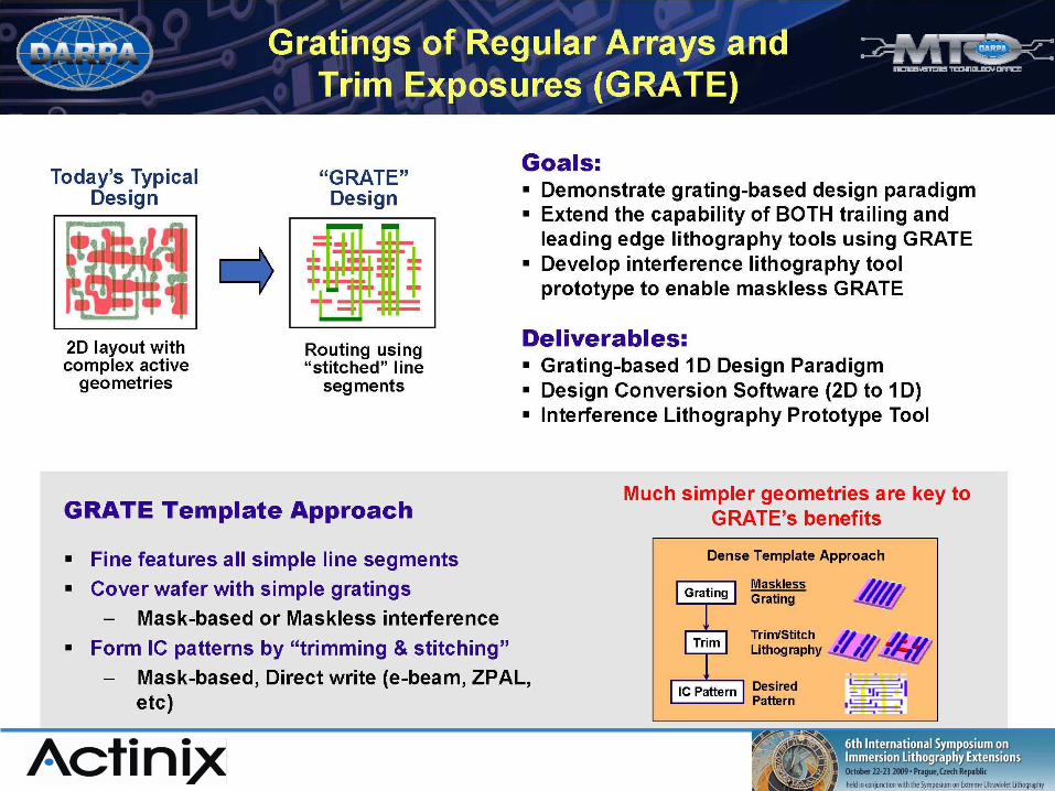
• Why LIIL? Potentially very low cost, maskless process for 35-25 nm hp using water and gen 2 and 3 fluids
• Main Issues: Full-field exposures and new circuit libraries (2D to 1D)
• Enabling technology: long coherence length, far-UV laser (=197 nm) being developed by Actinix/Sandia under a DARPA STTR for low volume nano-fab
• This laser development project is related to upcoming DARPA program, GRATE: Gratings of Regular Arrays and Trim Exposures
• Pending proposal on a full-field LIIL R&D tool for testing new nano-scale metrology methods and protocols essential for next generation semiconductor device production
• Tool will support investigations into fringe doubling and directed self-assembly (DSA) as viable next generation litho processes (< 16 nm hp).

Interference Lithography Tools - Some Examples
• 257 nm - IBM, UNM• 248 nm - RIT• 213 nm - UNM• 193 nm - RIT (Amphibian), IBM Nemo• 157 nm - MIT LL• EUV - Intel, Hanyang Univ., Paul Scherrer Inst., Univ. of Wisconsin
Micro-exposure Tools
• Meter scale gratings • 351 nm (Ar ion), Dry• High precision metrology• Transparent substrates• Scanned small field, 1 mm• Approx. 100 nm hp
MIT NanoRuler - Scanning beam interference litho (SBIL)
IBM Nemo
http://snl.mit.edu/

LIIL Tool: IBM Nemo
• Laser: 193 nm, 7 pm, 25 mW, 5 kHz• High spatial coherence, TEM00 • Liquid Immersion: H2O, Gen II• 35 - 30 nm hp• Millimeter field size• High contrast > 90%

197 nm vs 193 nm : High index fluids have less transmission loss
3X lower absorption in IF-132 @ 197 nm
Second Generation Fluids for 193 nm Immersion Lithography, R. French, et al. SPIE Microlithography 2007.
Lower Less heating Lower n Less Distortion
• Increase source by 2%
• Move away from band edge
• Higher index liquidsmore feasible
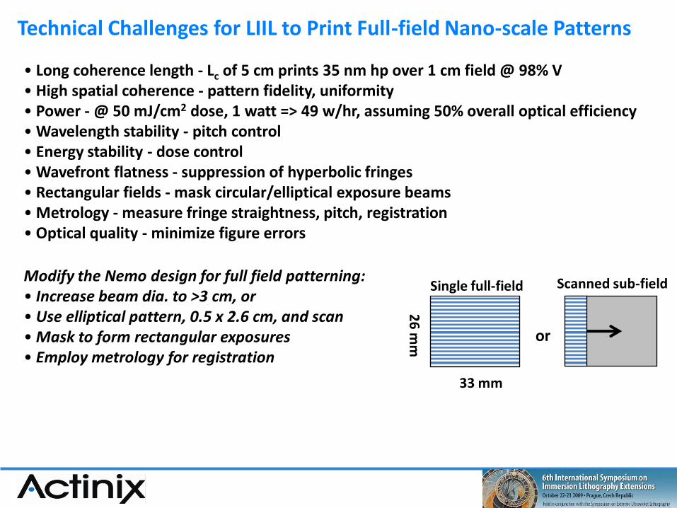
Technical Challenges for LIIL to Print Full-field Nano-scale Patterns
• Long coherence length - Lc of 5 cm prints 35 nm hp over 1 cm field @ 98% V• High spatial coherence - pattern fidelity, uniformity• Power - @ 50 mJ/cm2 dose, 1 watt => 49 w/hr, assuming 50% overall optical efficiency• Wavelength stability - pitch control• Energy stability - dose control• Wavefront flatness - suppression of hyperbolic fringes• Rectangular fields - mask circular/elliptical exposure beams• Metrology - measure fringe straightness, pitch, registration• Optical quality - minimize figure errors
Modify the Nemo design for full field patterning:• Increase beam dia. to >3 cm, or • Use elliptical pattern, 0.5 x 2.6 cm, and scan• Mask to form rectangular exposures• Employ metrology for registration
33 mm
26
mm or
Single full-field Scanned sub-field
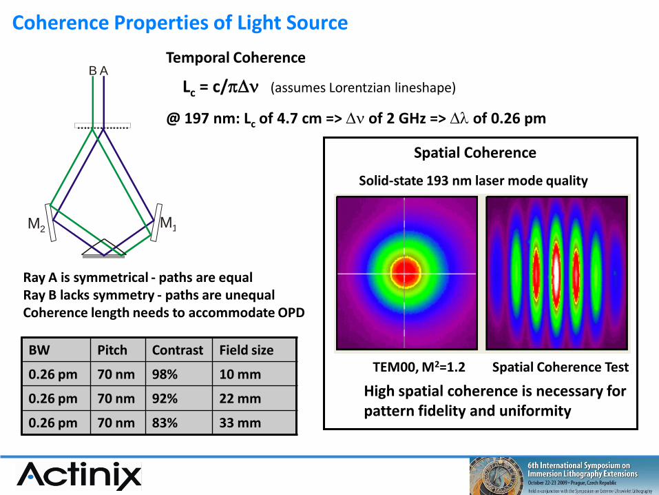
Coherence Properties of Light Source
Ray A is symmetrical - paths are equalRay B lacks symmetry - paths are unequalCoherence length needs to accommodate OPD
BW Pitch Contrast Field size
0.26 pm 70 nm 98% 10 mm
0.26 pm 70 nm 92% 22 mm
0.26 pm 70 nm 83% 33 mm
M2M1
AB
Solid-state 193 nm laser mode quality
TEM00, M2=1.2 Spatial Coherence Test
High spatial coherence is necessary for pattern fidelity and uniformity
Spatial Coherence
Temporal Coherence
Lc = c/
@ 197 nm: Lc of 4.7 cm => of 2 GHz => of 0.26 pm
(assumes Lorentzian lineshape)
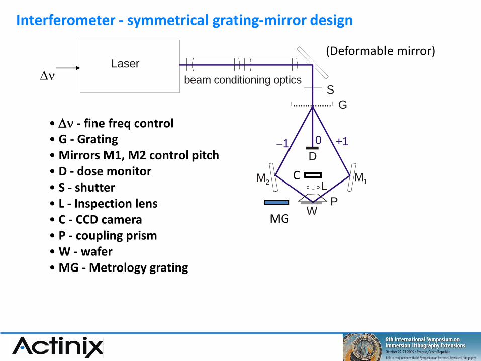
Interferometer - symmetrical grating-mirror design
• - fine freq control• G - Grating• Mirrors M1, M2 control pitch• D - dose monitor• S - shutter• L - Inspection lens • C - CCD camera• P - coupling prism• W - wafer• MG - Metrology grating
(Deformable mirror)
0 +11
M2M1
WP
L
G
S
D
Laser
beam conditioning optics
C
MG

Beam shapingSuper-gaussian profiles
Second lens corrects the wavefrontdistortion due to the first lens,
First lens redistributes rays to transform the intensity profile
Collimated beam with planar wavefront
Efficiency vs uniformity
Keplerian-type anamorphic telescope
p=16
p=8
p=4
p=2 (Gaussian)
p=2
p=4
p=8
p=12

Metrology – Pitch Control• Rectangular interference pattern illumination - full chip field (or scanned over field)
33 mm
L=N=26 mm
pitch ofinterference pattern
• Registration requirements (~10% of pitch) = 0.1 x 70 nm = 7 nm
distortion L 7 nm over field
tolerance on pitch
• Tolerance on: , n, T,
• Can use precise control of to help maintain registration across field
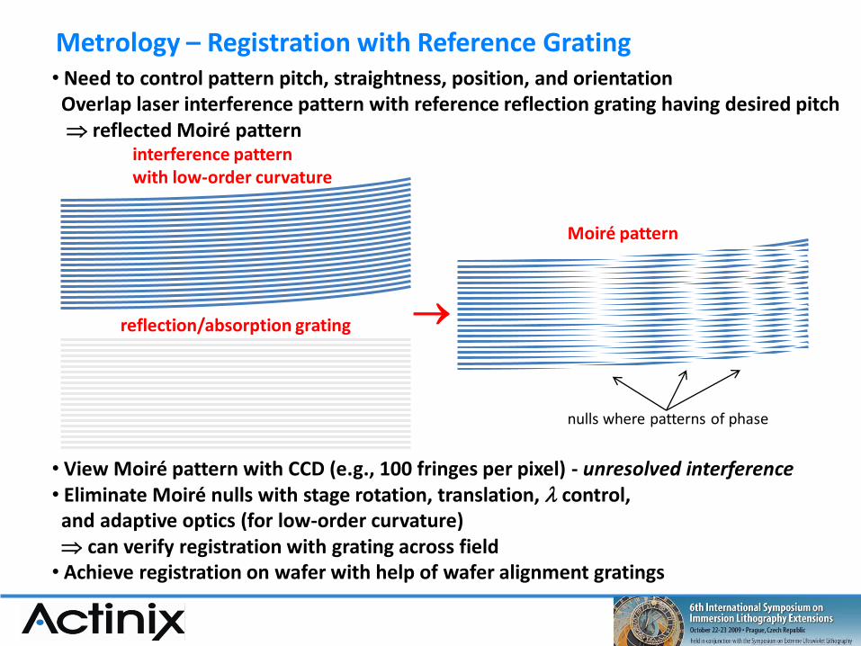
Metrology – Registration with Reference Grating• Need to control pattern pitch, straightness, position, and orientationOverlap laser interference pattern with reference reflection grating having desired pitch reflected Moiré pattern
interference patternwith low-order curvature
reflection/absorption grating
• View Moiré pattern with CCD (e.g., 100 fringes per pixel) - unresolved interference• Eliminate Moiré nulls with stage rotation, translation, control, and adaptive optics (for low-order curvature) can verify registration with grating across field
• Achieve registration on wafer with help of wafer alignment gratings
Moiré pattern
nulls where patterns of phase
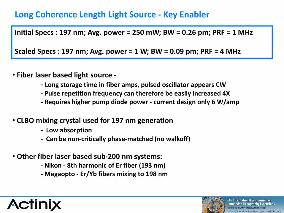
Long Coherence Length Light Source - Key Enabler
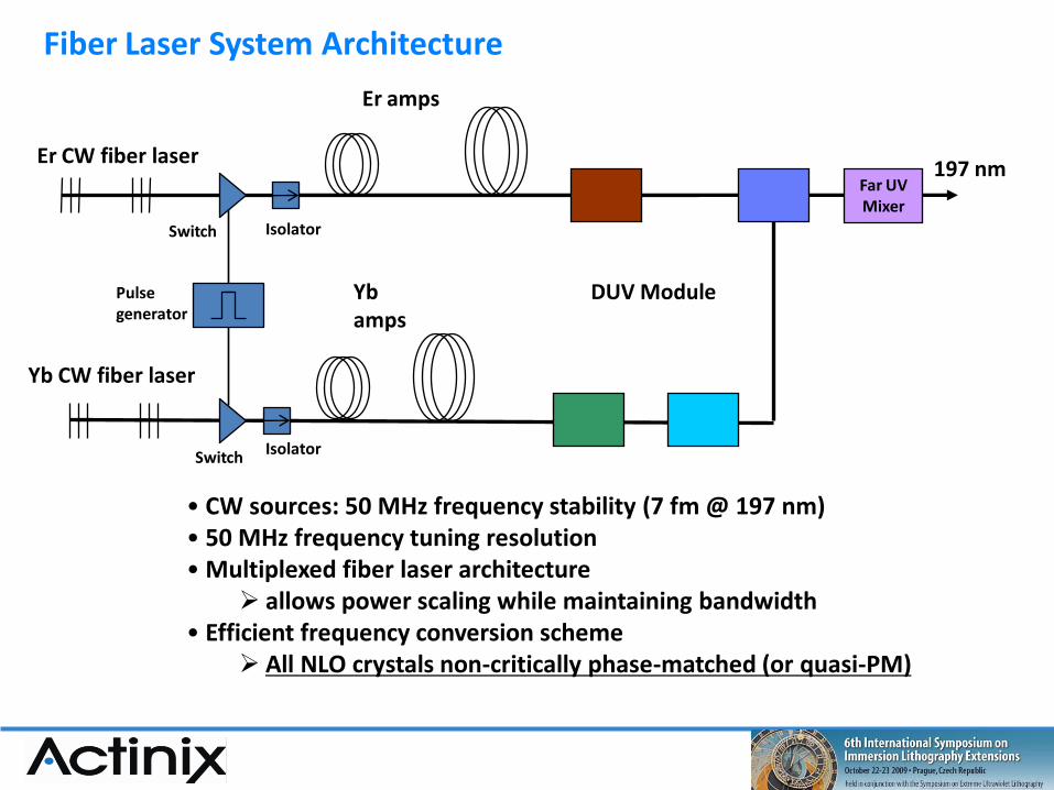
• Fiber laser based light source -- Long storage time in fiber amps, pulsed oscillator appears CW- Pulse repetition frequency can therefore be easily increased 4X- Requires higher pump diode power - current design only 6 W/amp
• CLBO mixing crystal used for 197 nm generation - Low absorption- Can be non-critically phase-matched (no walkoff)
• Other fiber laser based sub-200 nm systems:- Nikon - 8th harmonic of Er fiber (193 nm)- Megaopto - Er/Yb fibers mixing to 198 nm
Initial Specs : 197 nm; Avg. power = 250 mW; BW = 0.26 pm; PRF = 1 MHz
Scaled Specs : 197 nm; Avg. power = 1 W; BW = 0.09 pm; PRF = 4 MHz

Far-UV moduleDUV Module
Infra-red front end
Solid-state Far-UV Generation

Fiber Amplifiers: Design for Low Self Phase Modulation
x
Pulse duration = 2 ns; Energy = 2.6 J (P = 2.6 watts)Power scalable - increase PRF to 4 KHz, P = 10 watts
Modeled phase distortion for our design
0.75 rad
Modeled spectrum assuming 2.0 rad phase
Our operating point300 MHzFWHM
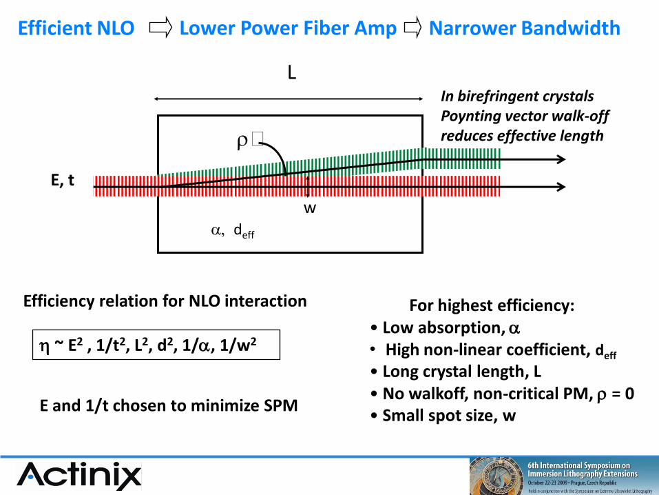
In birefringent crystalsPoynting vector walk-off reduces effective length
L
deff
• Low absorption, •High non-linear coefficient, deff
• Long crystal length, L• No walkoff, non-critical PM, = 0• Small spot size, w
Efficient NLO Lower Power Fiber Amp Narrower Bandwidth
~ E2 , 1/t2, L2, d2, 1/, 1/w2
E, t
w
Efficiency relation for NLO interaction For highest efficiency:
E and 1/t chosen to minimize SPM
Far UVMixer
Er amps
Yb amps
Switch
Switch
Er CW fiber laser197 nm
Isolator
Isolator
Yb CW fiber laser
Pulse generator
• CW sources: 50 MHz frequency stability (7 fm @ 197 nm)• 50 MHz frequency tuning resolution• Multiplexed fiber laser architecture
allows power scaling while maintaining bandwidth• Efficient frequency conversion scheme
All NLO crystals non-critically phase-matched (or quasi-PM)
Fiber Laser System Architecture
DUV Module

Summary
• Liquid immersion interference lithography is a tractable low cost solution for single exposure patterning offull field grating structures down to 25 nm hp
• 197 nm fiber-based laser will provide coherence length, beam quality and power suitable for printing high contrast gratings at reasonable throughput
• Interferometer design needs to incorporate metrology and possibly adaptive optical techniques to control fringes over full-field