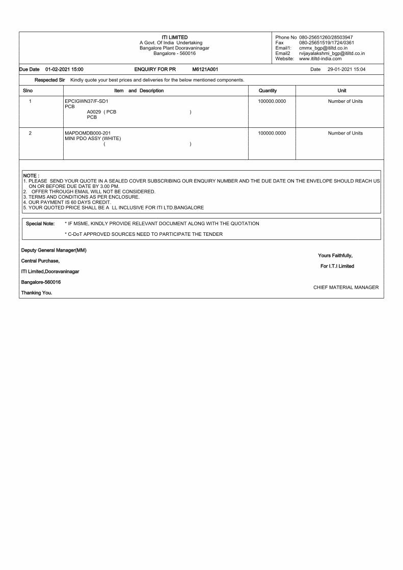
ITI LIMITED Phone No 080-25651519/1724/0361 Bangalore ...
8
( ( 2. and 1 2 Slno Item A0029 Date Unit Phone No Fax Email1: Email2 Website: Due Date 100000.0000 100000.0000 Special Note: Quantity Number of Units Number of Units Respected Sir ENQUIRY FOR PR ) ) 29-01-2021 15:04 01-02-2021 15:00 For I.T.I Limited Yours Faithfully, PCB CHIEF MATERIAL MANAGER 5. YOUR QUOTED PRICE SHALL BE A 080-25651260/28503947 080-25651519/1724/0361 [email protected] [email protected] www.itiltd-india.com Description ITI LIMITED Bangalore - 560016 M6121A001 A Govt. Of India Undertaking Bangalore Plant Dooravaninagar PCB 1. PLEASE SEND YOUR QUOTE IN A SEALED COVER SUBSCRIBING OUR ENQUI EPCIGWN37/F-SD1 PCB MAPDOMDB000-201 MINI PDO ASSY (WHITE) RY NUMBER AND THE DUE DATE ON THE ENVELOPE SHOULD REACH US LL INCLUSIVE FOR ITI LTD.BANGALORE Kindly quote your best prices and deliveries for the below mentioned components. * IF MSME, KINDLY PROVIDE RELEVANT DOCUMENT ALONG WITH THE QUOTATION * C-DoT APPROVED SOURCES NEED TO PARTICIPATE THE TENDER OFFER THROUGH EMAIL WILL NOT BE CONSIDERED. ON OR BEFORE DUE DATE BY 3.00 PM. NOTE : 3. TERMS AND CONDITIONS AS PER ENCLOSURE. 4. OUR PAYMENT IS 60 DAYS CREDIT. Deputy General Manager(MM) Central Purchase, ITI Limited,Dooravaninagar Bangalore-560016 Thanking You.
Transcript of ITI LIMITED Phone No 080-25651519/1724/0361 Bangalore ...
(
(
2.
and
1
2
Slno Item
A0029
Date
Unit
Phone NoFaxEmail1:Email2Website:
Due Date
100000.0000
100000.0000
Special Note:
Quantity
Number of Units
Number of Units
Respected Sir
ENQUIRY FOR PR
)
)
29-01-2021 15:0401-02-2021 15:00
For I.T.I Limited
Yours Faithfully,
PCB
CHIEF MATERIAL MANAGER
5. YOUR QUOTED PRICE SHALL BE A
080-25651260/28503947080-25651519/1724/[email protected][email protected]
Description
ITI LIMITED
Bangalore - 560016
M6121A001
A Govt. Of India UndertakingBangalore Plant Dooravaninagar
PCB
1. PLEASE SEND YOUR QUOTE IN A SEALED COVER SUBSCRIBING OUR ENQUI
EPCIGWN37/F-SD1PCB
MAPDOMDB000-201MINI PDO ASSY (WHITE)
RY NUMBER AND THE DUE DATE ON THE ENVELOPE SHOULD REACH US
LL INCLUSIVE FOR ITI LTD.BANGALORE
Kindly quote your best prices and deliveries for the below mentioned components.
* IF MSME, KINDLY PROVIDE RELEVANT DOCUMENT ALONG WITH THE QUOTATION
* C-DoT APPROVED SOURCES NEED TO PARTICIPATE THE TENDER
OFFER THROUGH EMAIL WILL NOT BE CONSIDERED.ON OR BEFORE DUE DATE BY 3.00 PM.
NOTE :
3. TERMS AND CONDITIONS AS PER ENCLOSURE.4. OUR PAYMENT IS 60 DAYS CREDIT.
Deputy General Manager(MM)
Central Purchase,
ITI Limited,Dooravaninagar
Bangalore-560016
Thanking You.

ANT
RST
OFF ETH5V ANT
lh&MkWVC-DOT
mini PDO
R
AutoCAD SHX Text
A
AutoCAD SHX Text
B
AutoCAD SHX Text
C
AutoCAD SHX Text
D
AutoCAD SHX Text
E
AutoCAD SHX Text
F
AutoCAD SHX Text
1
AutoCAD SHX Text
2
AutoCAD SHX Text
3
AutoCAD SHX Text
4
AutoCAD SHX Text
5
AutoCAD SHX Text
6
AutoCAD SHX Text
7
AutoCAD SHX Text
8
AutoCAD SHX Text
F
AutoCAD SHX Text
E
AutoCAD SHX Text
D
AutoCAD SHX Text
C
AutoCAD SHX Text
B
AutoCAD SHX Text
A
AutoCAD SHX Text
8
AutoCAD SHX Text
7
AutoCAD SHX Text
6
AutoCAD SHX Text
5
AutoCAD SHX Text
4
AutoCAD SHX Text
3
AutoCAD SHX Text
2
AutoCAD SHX Text
1
AutoCAD SHX Text
is not allowed without written consent of the proprietors.
AutoCAD SHX Text
Reproduction, utilisation or disclosure to third parties in any form whatsoever
AutoCAD SHX Text
This document is the property of CENTRE FOR DEVELOPMENT OF TELEMATICS.
AutoCAD SHX Text
NUMBER
AutoCAD SHX Text
C-DOT
AutoCAD SHX Text
TELEMATICS
AutoCAD SHX Text
CENTRE FOR DEVELOPMENT OF
AutoCAD SHX Text
SCALE
AutoCAD SHX Text
DIMNS
AutoCAD SHX Text
MM
AutoCAD SHX Text
IN
AutoCAD SHX Text
APPROVED
AutoCAD SHX Text
DATE
AutoCAD SHX Text
CHECKED
AutoCAD SHX Text
DRAWN
AutoCAD SHX Text
MATERIAL
AutoCAD SHX Text
DATE
AutoCAD SHX Text
DATE
AutoCAD SHX Text
DOC
AutoCAD SHX Text
CODE
AutoCAD SHX Text
NUMBER
AutoCAD SHX Text
ISS
AutoCAD SHX Text
ECO No
AutoCAD SHX Text
CHANGE
AutoCAD SHX Text
CHKD
AutoCAD SHX Text
APPD
AutoCAD SHX Text
PROJECTION
AutoCAD SHX Text
FINISH
AutoCAD SHX Text
TOLERANCES
AutoCAD SHX Text
INT. AXES
AutoCAD SHX Text
GENERAL
AutoCAD SHX Text
DIAGONAL
AutoCAD SHX Text
DIAMETER
AutoCAD SHX Text
BEND. ANG.
AutoCAD SHX Text
BEND. RAD.
AutoCAD SHX Text
FLATNESS
AutoCAD SHX Text
CONCENTRICITY
AutoCAD SHX Text
UNSPECIFIED TOLS. AS PER IS 2102-1980
AutoCAD SHX Text
NEXT ASSY
AutoCAD SHX Text
A2
AutoCAD SHX Text
SIZE
AutoCAD SHX Text
TITLE
AutoCAD SHX Text
OF
AutoCAD SHX Text
SHEET No
AutoCAD SHX Text
ISS
AutoCAD SHX Text
NUMBER
AutoCAD SHX Text
ITEM
AutoCAD SHX Text
QTY
AutoCAD SHX Text
DATE
AutoCAD SHX Text
BANGALORE
AutoCAD SHX Text
ORIGINAL
AutoCAD SHX Text
01
AutoCAD SHX Text
PROTO RELEASE
AutoCAD SHX Text
MAP-DOMDC000-201
AutoCAD SHX Text
MINI PDO ASSY-2
AutoCAD SHX Text
MAP-DOMDC000-201
AutoCAD SHX Text
1:1
AutoCAD SHX Text
GA
AutoCAD SHX Text
01
AutoCAD SHX Text
%%P0,1
AutoCAD SHX Text
%%P0,2
AutoCAD SHX Text
Ashish/Ramesh
AutoCAD SHX Text
Srinivas
AutoCAD SHX Text
Srin ivas
AutoCAD SHX Text
1 1
AutoCAD SHX Text
(WHITE)
AutoCAD SHX Text
(REF)
AutoCAD SHX Text
(REF)
AutoCAD SHX Text
DESCRIPTION
AutoCAD SHX Text
NO.
AutoCAD SHX Text
ITEM
AutoCAD SHX Text
QTY
AutoCAD SHX Text
1
AutoCAD SHX Text
PART NO.
AutoCAD SHX Text
1
AutoCAD SHX Text
TOP COVER
AutoCAD SHX Text
6
AutoCAD SHX Text
7
AutoCAD SHX Text
8
AutoCAD SHX Text
1
AutoCAD SHX Text
LIGHT PIPE
AutoCAD SHX Text
1
AutoCAD SHX Text
BOTTOM COVER
AutoCAD SHX Text
4
AutoCAD SHX Text
ANTI SKID PAD
AutoCAD SHX Text
2
AutoCAD SHX Text
4
AutoCAD SHX Text
(MINI PDO)
AutoCAD SHX Text
(TITLI)
AutoCAD SHX Text
(TITLI)
AutoCAD SHX Text
2
AutoCAD SHX Text
1
AutoCAD SHX Text
3
AutoCAD SHX Text
4
AutoCAD SHX Text
5
AutoCAD SHX Text
MCT-MPGEN127-401
AutoCAD SHX Text
SCR TAPPING XREC-3x8,0
AutoCAD SHX Text
4, 8
AutoCAD SHX Text
4
AutoCAD SHX Text
2, 7
AutoCAD SHX Text
6
AutoCAD SHX Text
4
AutoCAD SHX Text
2
AutoCAD SHX Text
5
AutoCAD SHX Text
MPP-DOMDC001-201
AutoCAD SHX Text
MPT-TLDKA003-401
AutoCAD SHX Text
MPT-TLDKA004-101
AutoCAD SHX Text
SCR TAPPING XREC-3x13,0
AutoCAD SHX Text
MCS-PHCRR007-401
AutoCAD SHX Text
MCS-PHCRR016-401
AutoCAD SHX Text
21/12/2020
AutoCAD SHX Text
epg_IGW_pdr.dwg
AutoCAD SHX Text
1
AutoCAD SHX Text
ANTENNA PLATE
AutoCAD SHX Text
(MINI PDO)
AutoCAD SHX Text
MPP-DOMDC002-401
AutoCAD SHX Text
1
AutoCAD SHX Text
TOP COVER STICKER
AutoCAD SHX Text
(MINI PDO)
AutoCAD SHX Text
MPP-DOMDC004-401
AutoCAD SHX Text
1
AutoCAD SHX Text
D:\Ramesh_epg\Ramesh_epg1\Ramesh_projects\SDCN\IGW
AutoCAD SHX Text
3
AutoCAD SHX Text
4
AutoCAD SHX Text
%%UVIEW-A
AutoCAD SHX Text
A
AutoCAD SHX Text
21.12.20
AutoCAD SHX Text
21.12.20
AutoCAD SHX Text
21.12.20


PCB FILM RELEASE CHECKLIST (To be sent to Vendor Along with Design Data)
IR No :8933 QCR Reference : Date:08-03-2019
PCB DESCRIPTION C-dot Part Number of PCB EPC-IGWN37/F-SD1 Name of the PCB IOT gateway card No of Layers : 4 Density Classification :
PCB Size: Length
Breadth Unit Thickness
100 X 70 mm 1.6 mm Panel Size: - Number of PCBs per Panel : 8
DESIGN & DRILL DATA Input type : Gerber Files Qty 11 Input Code : Others
Number Format :
Units : Inches
Zero Omit : None
Coordinates: Absolute
Scale : 1:1
DRC CHECKS FOR SIGNAL LAYERS
Minimum Track width : Inner Layer- na Outer Layer 5 mils
Minimum Spacing between Tracks : Inner Layer- na Outer Layer 8 mils
Minimum Spacing between Pad & Track: Inner Layer 8 mils Outer Layer 8 mils
Minimum PTH Size: 10 mils
Minimum Annular Ring: 4 mils
Minimum SMD Pitch: 19.7 mils
FILM & GERBER DETAILS Description Films File Name Description Films File Name
Drill DRL IGWN01 DRL.GBX Etch Layer 17
L17.GBX
Solder Paste Top SPT IGWN01 SPT.GBX Etch Layer 18
L18.GBX
Legend Top LGT IGWN01 LGT.GBX Etch Layer 19
L19.GBX
Solder Mask Top SMT IGWN01 SMT.GBX Etch Layer 20
L20.GBX
Etch Layer 1 L01 IGWN01 L01.GBX Etch Layer 21
L21.GBX
Etch Layer 2 L02 IGWN01 L02.GBX Etch Layer 22
L22.GBX
Etch Layer 3 L03 IGWN01 L03.GBX Etch Layer 23
L23.GBX
Etch Layer 4 L04 IGWN01 L04.GBX Etch Layer 24
L24.GBX
Etch Layer 5
L05.GBX Etch Layer 25
L25.GBX
Etch Layer 6
L06.GBX Etch Layer 26
L26.GBX
Etch Layer 7
L07.GBX Etch Layer 27
L27.GBX
Etch Layer 8
L08.GBX Etch Layer 28
L28.GBX
Etch Layer 9
L09.GBX Etch Layer 29
L29.GBX
Etch Layer 10
L10.GBX Etch Layer 30
L30.GBX
Etch Layer 11
L11.GBX Solder Mask Bottom SMB IGWN01 SMB.GBX
Etch Layer 12
L12.GBX Legend Bottom LGB IGWN01 LGB.GBX
Etch Layer 13
L13.GBX Solder Paste Bottom SPB IGWN01 SPB.GBX
Etch Layer 14
L14.GBX NC Drill NCD IGWN01 NCD.TXT

Etch Layer 15
L15.GBX NC Drill Tool Set NCT IGWN01 NCT.TXT
Etch Layer 16
L16.GBX Decode List DCL IGWN01 DCL.TXT
PCB FILM RELEASE CHECKLIST (To be sent to Vendor Along with Design Data)
MANUFACTURING DETAILS
Soder Mask Type : Photo Imageable
Minimum Solder Mask Clearance : 2 mils
Legend On (Side) : Both
Design Technology Mixed
Special Requirements :
Controlled Impedance : Yes No of Impedance layers : 2 Impedance Value : 50 E
Base Material NEMA FR4 (glass epoxy)-High Tg
If base material is other than FR4 please provide complete details of the material:
Surface Finish Electroless gold over nickel
Gold Plating required for Edge fingers No of Edge Fingers/Total Area (Specify , if the option is 'yes')
Nos/ Sq Inches
Automatic Copper Balancing Allowed Yes
Tear Drop Triangular
Constructional Details Drawing No igwSD1-PCB-SPEC.doc
MISCELLANEOUS DETAILS
APPROVALS
Designer Name Approved by
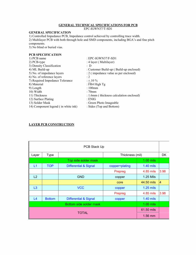
GENERAL TECHNICAL SPECIFICATIONS FOR PCB EPC-IGWN37/T-SD1
GENERAL SPECIFICATION 1) Controlled Impedance PCB, Impedance control achieved by controlling trace width. 2) Multilayer PCB with both through hole and SMD components, including BGA’s and fine pitch components. 3) No blind or buried vias. PCB SPECIFICATION 1) PCB name : EPC-IGWN37/F-SD1 2) PCB-type : 4 layer ( Multilayer) 3) Density Classification : D 4) ML Build-up : Customer Build-up ( Build-up enclosed) 5) No. of impedance layers : 2 ( impedance value as per enclosed) 6) No. of reference layers : 2 7) Required Impedance Tolerance : + 10 % 8) Material : FR4 High Tg 9) Length : 100mm 10) Width : 70mm 11) Thickness : 1.6mm ( thickness calculation enclosed) 12) Surface Plating : ENIG 13) Solder Mask : Green Photo Imageable 14) Component legend ( in white ink) : Sides (Top and Bottom)
LAYER PCB CONSTRUCTION
PCB Stack Up
Layer Type Thickness (mil) DK
Top side solder mask 1.00 mils
L1 TOP Differential & Signal copper+plating 1.40 mils
Prepreg 4.85 mils 3.98
L2 GND copper 1.25 Mils
core 44.50 mils 4
L3 VCC copper 1.25 mils
Prepreg 4.85 mils 3.98
L4 Bottom Differential & Signal copper 1.40 mils
Bottom side solder mask 1.00 mils
TOTAL 61.50 mils
1.56 mm

Total Thickness : 61.50 mils +/- 10%
Controlled impedance for single ended and diff signals as per below table:
Layer Cont. Imp. Ref. Layer Trace width
L1
S50 L2 8mil
S63 L2 5 mils
D100 L2 6.5/8.5/6.5mil
D90 L2 7.5/7.5/7.5mil
L4
S50 L3 8mil
S63 L3 5 mils
D100 L3 6.5/8.5/6.5mil
D90 L3 7.5/7.5/7.5mil