ISSUE 3 – June / July 2021 POWER ...
36
POWER SEMICONDUCTORS Benefits of CoolSiC MOSFETs in Bi-Directional Inverter Applications ISSUE 3 – June / July 2021 www.power-mag.com Also inside this issue Opinion | Market News Industry News | PCIM 2021 APEC 2021
Transcript of ISSUE 3 – June / July 2021 POWER ...

POWER SEMICONDUCTORS Benefits of CoolSiC MOSFETs in Bi-Directional Inverter Applications
ISSUE 3 – June / July 2021 www.power-mag.com
Also inside this issue Opinion | Market News Industry News | PCIM 2021 APEC 2021
01_pee_0321.qxp_p01 Cover 25/06/2021 06:52 Page 1

Hello PolarFire® FPGA: Innovation UnleashedReduce Your Design’s Total Power Up to 50%
Make low-power innovation possible with increased thermal headroom by leveraging our PolarFire FPGAs. Build your next product with increased compute capability, while solving key power design challenges.
Data processing is moving to the edge in industrial automation, communications, smart embedded vision and automotive electronics. PolarFire FPGA’s lower power enables more compute capability in these thermally constrained environments than competitive products.
Say Hello to PolarFire FPGAs and SoCs.
Key Features• Lowest-power, live at power up• Mid-range densities 50K–500K LEs• Smallest form factor 11 x 11 mm• 12.7 Gbps transceivers• 1.6 Gbps I/Os enable MIPI and DDR4• Best-in-class security and reliability
microchip.com/PolarFire
The Microchip name and logo, the Microchip logo and PolarFire are registered trademarks of Microchip
Technology Incorporated in the U.S.A. and other countries. All other trademarks are the property of their registered
owners. © 2021 Microchip Technology Inc. All rights reserved. DS00003918A. MEC2372-ENG-04-21
02_pee_0321.indd 1 25/06/2021 07:14
CONTENTS
www.power-mag.com Issue 3 2021 Power Electronics Europe
3
Editor Achim Scharf Tel: +49 (0)892865 9794 Fax: +49 (0)892800 132 Email: [email protected]
Production Editor Chris Davis Tel: +44 (0)1732 370340
Financial Manager Caren Brown Tel: +44 (0)1732 370340 Fax: +44 (0)1732 360034 Email: [email protected]
Reader/Circulation Enquiries Perception Tel: +44 (0) 1825 701520 Email: [email protected]
INTERNATIONAL SALES OFFICES Mainland Europe: Victoria Hufmann Norbert Hufmann Tel: +49 911 9397 643 Fax: +49 911 9397 6459 Email: [email protected]
Eastern US Ian Atkinson Tel: +44 (0)1732 370340 Fax: +44 (0)1732 360034 Email: [email protected] Western US and Canada Ian Atkinson Tel: +44 (0)1732 370340 Fax: +44 (0)1732 360034 Email: [email protected]
Japan: Yoshinori Ikeda, Pacific Business Inc Tel: 81-(0)3-3661-6138 Fax: 81-(0)3-3661-6139 Email: [email protected]
Taiwan Prisco Ind. Service Corp. Tel: 886 2 2322 5266 Fax: 886 2 2322 2205
Publisher & UK Sales Ian Atkinson Tel: +44 (0)1732 370340 Fax: +44 (0)1732 360034 Email: [email protected] www.power-mag.com
Circulation and subscription: Power Electronics Europe is available for the following subscription charges. Power Electronics Europe: annual charge UK/NI £95, overseas $160, EUR 150. Contact: DFA Media, 192 The High Street, Tonbridge, Kent TN9 1BE Great Britain. Tel: +44 (0)1732 370340. Fax: +44 (0)1732 360034. Refunds on cancelled subscriptions will only be provided at the Publisher’s discretion, unless specifically guaranteed within the terms of subscription offer.
Editorial information should be sent to The Editor, Power Electronics Europe, PO Box 340131, 80098 Munich, Germany.
The contents of Power Electronics Europe are subject to reproduction in information storage and retrieval systems. All rights reserved. No part of this publication may be reproduced in any form or by any means, electronic or mechanical including photocopying, recording or any information storage or retrieval system without the express prior written consent of the publisher.
Printed by: Warners.
ISSN 1748-3530
PAGE 6
Market News
PEE looks at the latest Market News and company developments
PAGE 10
Industry News
PAGE 12
PCIM 2021 PAGE 25
APEC 2021
Benefits of CoolSiC MOSFETs in Bi-Directional Inverter Applications With the move to renewable energy, there is an increased focus not only on generation but also storage, to make the most of the intermittent supply from wind and solar. Batteries are the common solution and costs are dropping, driven by the technology improvements stemming from the EV market. This opens up opportunities for energy storage at any scale, from domestic to utility. As the supply paradigm shifts towards renewables, traditional generation from carbon-based fuels reduces, but also interacts to its advantage by using distributed storage to feed AC back into the grid through inverters for ‘peak-shaving’, to make generation more cost effective and reliable. To achieve this, batteries need to be able to charge from a cheap or convenient energy source and then discharge to a local load or back into the utility grid as ‘feed in’. AC/DC chargers and DC/AC inverters are established products, but if they can be efficiently combined, then there are costs to be saved. As a result, there is intense interest in ‘bi-directional converters’, with the volume market set to be in households with a local renewable energy source and storage, which may be an EV battery. SiC MOSFETs are a natural evolution from Si superjunction MOSFETs for applications at medium to high power with high switching frequency. Here there are significant efficiency gains to be had, along with a reduction in size and cost of associated components, particularly magnetics. This can result in significant end-product savings in cost, size and weight, as well as lower energy bills. In bi-directional converters, SiC devices can perform all high voltage switching functions with higher efficiency than traditional solutions and with their superior body diode characteristics, can make hard switching topologies such as the totem-pole PFC viable and cost effective. As a demonstration of the advantages of SiC MOSFETs in a bi-directional converter, Infineon has showcased a 3.3 kW totem-pole PFC stage which achieves 4.7 W/cm? power density with a peak efficiency of 99.1 % at 230 VAC input and 400 VDC output. Efficiency also peaks at over 98.8 % when operating in inverter mode, generating 230 VAC at 50 Hz. More details on page. 22. Cover image supplied by Infineon Technologies
FEATURE STORY
To receive your
own copy of
Power Electronics Europe
subscribe today at:
www.power-mag.com
p03 Contents.qxp_p03 Contents 25/06/2021 07:06 Page 3

CALL FOR FUTURE PANELISTS for our online panel discussions Contact us at Drives & Controls for more information:Andy Wylie 01732 370341 [email protected] | Damien Oxlee 01732 370342 [email protected]
2021 Subjects and Broadcast Dates10am UK, Tue Mar 9 2021 Industrial Networks, IIOT and Communications* 10am UK, Tue Mar 9 2021 Plant Safety and Security* 10am UK, Tue May 11 2021 Robotics & Advanced Automation* 10am UK, Tue Jul 13 2021 Maintenance 4.0 10am UK, Tue Sep 14 2021 Digital Transformation in the UK 10am UK, Tue Nov 9 2021 3D printing/Additive Manufacturing
REGISTRATION NOW OPENhttps://tinyurl.com/yc3jo6db
* Recordings of pastpanel discussions can be view online at the link above
Talking Industry A4 house ad.qxp_Layout 1 12/05/2021 09:10 Page 1

OPINION 5
www.power-mag.com Issue 3 2021 Power Electronics Europe
According to Edoardo Merli’s APEC keynote physical limits prevent current Silicon technology from achieving the greater power density and miniaturization the market needs from power products to meet growing environmental concerns. As an alternative, wide-bandgap (WBG) power products are gaining traction in the market because of their energy efficiency and because they help address many of those environmental issues. For example, SiC and GaN WBG materials, which enable superior overall performance, are helping manufacturers attain remarkable gains in applications like traction inverter for SiC and adaptors/chargers for GaN. Still, Silicon products should co-exist with the WBG products owing to their cost-effectiveness in some low-power applications or whenever system performance is deemed adequate.
The GaN power market doubled in 2020 according to market researcher Yole, highlighting the growth of smartphone fast chargers and leading the way for telecom and automotive markets. In the consumer market, GaN enjoyed a successful year in 2020 thanks to several companies, such as Xiaomi, Lenovo, Samsung, Realme, Dell and LG, as well as other Chinese aftermarket companies that adopted GaN technology. Yole expects the GaN consumer power supply market to be the main driver, as this market is forecast to grow from almost $29 million in 2020 to around $670 million in 2026 with a CAGR of 70 %. The adoption of GaN in the smartphone market is fueled by system compactness, high efficiency, and adapter multifunctionalities. Fast charging is likely to be the killer application for the GaN power
device market. So far, at least 10 smartphones OEMs have launched more than 18 phones with an inbox GaN charger. This growth will continue in the aftermarket as well, with companies like Apple, Xiaomi, and Samsung opting for an out-of-the-box charger solution. Power Integrations recently launched the InnoSwitch4-CZ family of high frequency, zero voltage switching (ZVS) flyback switcher ICs. InnoSwitch4-CZ devices incorporate a robust 750 V GaN primary switch and a novel high frequency active clamp flyback controller to facilitate a new class of ultra-compact chargers suitable for phones, tablets, and laptops. The first consumer devices based on InnoSwitch4-CZ devices were introduced earlier by Anker. The InnoSwitch4-CZ and ClampZero combination provides up to 95 % efficiency and maintains very high efficiency across variations in line voltage, system load and output voltage. According to Anker’s CEO, these outstanding levels of integration and efficiency are key to the Nano II series’ extremely compact design.
In the telecom & datacom market, which requires more efficient, smaller power supply amidst tighter regulations for energy consumption, datacenter & telecom operators are already interested in GaN devices. Following the first small-volume adoption of GaN-based power supplies by Eltek, Delta, and BelPower in recent years, Yole expects a larger penetration of GaN, with a market valued at $9 million in 2020 and a CAGR 2020-2026 of 70 %, reaching more than $220 million in 2026.
The automotive & mobility market is also paying lots of attention to GaN, following big incentives for the electrification of cars and the interest in increasing driving range through system efficiency optimization. Players such as EPC, Transphorm, GaN Systems, Texas Instruments and Nexperia are AEC qualified. The major IDM STMicroelectronics, through partnership and acquisition, is also targeting GaN for EVs. Starting from 2022, GaN is expected to penetrate in small volumes in applications such as OBC and DC/DC converters.
Achieving operating voltages higher than 650 V has been challenged by the difficulty of growing thick-enough GaN buffer layers on 200 mm wafers. Therefore, SiC so far remains the semiconductor of choice for 650-1200 V applications – including electric cars and renewable energy. Now Belgium-based imec and Germany-based AIXTRON have demonstrated epitaxial growth of GaN buffer layers qualified for 1200 V applications on 200 mm substrates with a hard breakdown exceeding 1800 V. According to imec, GaN can now become the technology of choice for a whole range of operating voltages from 20 V to 1200 V. Being processable on larger wafers in high-throughput CMOS fabs, power technology based on GaN offers a significant cost advantage compared to the intrinsically expensive SiC-based technology.
Since PEE’s start in 1999 we have promoted new technologies such as WBGs and were convinced on their future. Thus examples of WBG achievements and applications can be found throughout this issue, particularly in the PCIM and APEC reports as well as in cover story.
Enjoy reading
Achim Scharf
PEE Editor
The WBG Train Accelerates
05_pee_0321.qxp_p05 Opinion 24/06/2021 14:07 Page 5

6 MARKET NEWS
Issue 3 2021 Power Electronics Europe www.power-mag.com
The GaN power market doubled in 2020 according to market researcher Yole, highlighting the impressive growth of smartphone fast chargers and leading the way for telecom and automotive markets.
“Following Oppo’s adoption of GaN in its 65 W inbox fast chargers for its Reno Ace model in late 2019, several phone OEMs and accessory charger providers released GaN-solution design wins for their fast chargers in 2020”, commented Ahmed Ben Slimane, Technology & Market Analyst at Yole Développement. “The GaN power market doubled in 2020 compared to 2019 and is poised to surpass the $1 billion mark in 2026. As further confirmation of this impressive GaN market growth, is that the markets for telecom & datacom and automotive & mobility will contribute in the mid- to long-term to overall growth, benefiting from GaN’s ascension in fast chargers.”
As analyzed by Yole’s team in the GaN Power 2021 Trends report, in the consumer market, GaN enjoyed a successful year in 2020 thanks to several companies, such as Xiaomi, Lenovo, Samsung, Realme, Dell and LG, as well as other Chinese aftermarket companies that adopted GaN technology. Yole expects the GaN consumer power supply market to be the main driver, as this market is forecast to grow from almost $29 million in 2020 to around $670 million in 2026 with a CAGR of 70 %. The adoption of GaN in the smartphone market is fueled by system compactness, high efficiency, and adapter multifunctionalities. Fast charging is likely to be the killer application for the GaN power device market. So far, at least 10 smartphones OEMs have launched more than 18 phones with an inbox GaN charger. This growth will continue in the aftermarket as well, with companies like Apple, Xiaomi, and Samsung opting for an out-of-the-box charger solution.
In the telecom & datacom market, which requires more efficient, smaller power supply amidst tighter regulations for energy consumption, datacenter & telecom operators are already interested in GaN devices. While GaN continues its ascension in the mass consumer market, the markets for telecom & datacom will benefit from the “economy of scale effect” and price erosion. Indeed, in these markets where reliability and cost are paramount, Yole expects that GaN penetration will see increasing volumes starting from 2023 – 2024. Following the first small-volume adoption of GaN-based power supplies by Eltek, Delta, and BelPower in recent years, Yole expects a larger penetration of GaN, with a market valued at $9 million in 2020 and a CAGR 2020-2026 of 70 %, reaching more than $220 million in 2026.
“The automotive & mobility market is also paying lots of attention to GaN, following big incentives for the electrification of cars and the interest in increasing driving range through system efficiency optimization. Players such as EPC, Transphorm, GaN Systems, Texas Instruments and Nexperia are AEC qualified. The major IDM STMicroelectronics, through partnership and acquisition, is also targeting GaN for EVs. Starting from 2022, GaN is expected to penetrate in small volumes in applications such as OBC and DC/DC converters, mainly related to sampling by OEM s and Tier-1s. Yole expects the automotive & mobility market to reach more than $155 million in 2026. In the long term, in cases where GaN has proven its reliability and high-current capabilities at a lower price, it can penetrate the more challenging EV/HEV inverter market and the conservative industrial market, which could create
remarkable high-volume opportunities for GaN. In fact, Nexperia and VisIC are working on GaN solutions for xEV inverters to compete with SiC and Si,” Ahmed Ben Slimane stated.
Regarding market players, Power Integrations and Navitas increased their market share within the power GaN market thanks to the fast-charging application for smartphones. STMicroelectronics has strengthened its position and product portfolio through its collaboration with TSMC, and the acquisition of majority stakes of Exagan. Texas Instruments and GaN systems have lately
qualified their GaN device for automotive applications. EPC, Transphorm, and Infineon pursue their penetration within several applications to name a few the datacenter and aerospace markets.
www.yole.fr
GaN Power Market Crosses $1 Billion in 2026
Belgium-based Imec and Germany-based AIXTRON have demonstrated epitaxial growth of GaN buffer layers qualified for 1200 V applications on 200 mm QST® substrates, with a hard breakdown exceeding 1800 V. The manufacturability of 1200 V-qualified buffer layers opens doors to highest voltage GaN-based power applications such as electric cars, previously only with SiC-based technology.
Wide-bandgap materials such as GaN and SiC have proved their value as next-generation semiconductors for power-demanding applications where Silicon falls short. SiC-based technology is the most mature, but it is also more expensive. Over the years tremendous progress has been made with GaN-based technology grown on for example 200 mm Si wafers. At imec, qualified
enhancement mode high-electron-mobility transistors (HEMTs) and Schottky diode power devices have been demonstrated for 100, 200 and 650 V operating voltage ranges, paving the way for high-volume manufacturing applications. However, achieving operating voltages higher than 650 V has been challenged by the difficulty of growing thick-enough GaN buffer layers on 200 mm wafers. Therefore, SiC so far remains the semiconductor of choice for 650-1200 V applications – including electric cars and renewable energy.
For the first time, imec and AIXTRON have demonstrated epitaxial growth of GaN buffer layers qualified for 1200 V applications on 200mm QST® (in SEMI standard thickness) substrates at 25°C and 150°C, with a hard breakdown exceeding 1800 V. “GaN can now become the technology of
GaN on 200 mm Wafers for 1200 V Applications
Market news.qxp_Layout 1 25/06/2021 07:48 Page 6

MARKET NEWS 7
www.power-mag.com Issue 3 2021 Power Electronics Europe
choice for a whole range of operating voltages from 20 V to 1200 V. Being processable on larger wafers in high-throughput CMOS fabs, power technology based on GaN offers a significant cost advantage compared to the intrinsically expensive SiC-based technology,” commented Denis Marcon, Senior Business Development Manager at imec. Key to achieving the high breakdown voltage is the careful engineering of the complex epitaxial material stack in combination with the use of 200 mm QST® substrates, executed in scope of the IIAP program The CMOS-fab friendly substrates from Qromis have a thermal expansion that closely matches the thermal expansion of the GaN/AlGaN epitaxial layers, paving the way for thicker buffer layers – and hence higher voltage operation.
“The successful development of imec’s 1200V GaN-on-QST epi-technology into our MOCVD reactor is a next step in our collaboration with imec. Earlier,
after having installed AIXTRON G5+C, imec’s proprietary 200 mm GaN-on-Si materials technology was qualified on our high-volume manufacturing platform, targeting for example high-voltage power switching and RF applications and enabling a rapid production ramp-up by pre-validated available epi-recipes. With this new achievement, we will be able to jointly tap into new markets. Currently, lateral e-mode devices are being processed to prove device performance at 1200 V, and efforts are ongoing to extend the technology towards even higher voltage applications. Next to this, imec is also exploring 8-inch GaN-on-QST vertical GaN devices to further extend the voltage and current range of GaN-based technology,” added AIXTRON’s CEO Felix Grawert.
www.imec-int.com
Infineon Expands SiC Supplier Base
Nexperia Invests To Boost Production Capacity
Infineon Technologies AG has concluded a supply contract with the Japanese wafer manufacturer Showa Denko K.K. for an extensive range of SiC including epitaxy. The German semiconductor manufacturer has thus secured more base material for the growing demand for SiC-based products.
The contract between Infineon and Showa Denko K.K. has a two-year term with an extension option. Infineon has a large portfolio of SiC semiconductors (CoolSiC MOSFETs and diodes) for industrial applications. “Our broad and fast growing portfolio demonstrates our leading role in supporting and shaping the market for SiC-based semiconductors which is expected to grow 30 to 40 percent annually over the next five years”, says Peter Wawer, President of the Industrial Power Control Division at Infineon. “The expansion of our supplier base with Showa Denko for wafers in this growth market marks an important step in our multisourcing strategy. It will support us to reliably meet the growing demand mid to long-term. Furthermore, we plan to collaborate with Showa Denko on the strategic development of the material to improve the quality while cutting costs at the same time.”
Regarding the semiconductor market in general Reinhard Ploss, CEO of Infineon, commented: “Demand greatly exceeds supply for the majority of applications. Infineon’s manufacturing facilities are running at full speed and we continue to invest in additional capacity. We see bottlenecks in those segments where we depend on chips supplied by foundries, especially in the case of automotive microcontrollers and IoT products. We are doing everything we can to provide our customers with the best possible support in this situation.”
For the second quarter of the 2021 fiscal year, Infineon generated income from continuing operations totaling €209 million, down on €256 million reported for the first quarter. The Automotive segment revenue rose from €1,150 million in the first quarter to €1,219 million in the second quarter, with almost all lines of business contributing to the 6 percent growth. In particular, demand for components for electric vehicles continued to develop
very positively. The Industrial segment revenue totaled €361 million in the second quarter of the current fiscal year, compared to €362 million in the preceding three-month period. A significant decline in revenue recorded for transportation was offset by growth in other areas, particularly power infrastructure and home appliances, but also renewable energy and industrial drives.
The company expects to generate revenue of between €2.6 billion and €2.9 billion in the third quarter. Revenue growth will continue to be held down by supply constraints, including the temporary shutdown of manufacturing facilities in Austin, Texas, in February, as well as capacity limitations at foundries. Based on its good performance in the first two quarters, and continuously strong momentum of the semiconductor market, Infineon again slightly raises its guidance for revenue for the fiscal year as a whole, despite tight capacities at foundries. Revenue is now forecast at around
€11.0 billion (plus or minus 3 percent). All segments are expected to benefit from an improving supply situation and continued growth in demand during second half FY 2021.
www.infineon.com
“Demand greatly exceeds supply for the majority of applications. Our manufacturing facilities are running at full speed and we continue to invest in additional capacity”, commented Infineon’s CEO Reinhard Ploss the current chip shortage
Nexperia has announced the next stage of its global growth strategy, confirming a $700 million investment over the next 12-15 months at its European wafer fabs, assembly factories in Asia and global R&D sites.
This investment will boost manufacturing capacity at all sites while supporting research and development into areas such as GaN and power management ICs. It will also underpin recruitment activities, with Nexperia looking to attract new chip designers and engineers. As a result, the capacity of the Hamburg fab in Germany – which currently produces more than 35,000 wafers (8-inch-equivalent) per month (70 billion semiconductors per year) – will further increase by 20 percent from mid-2022. While in the UK, at Nexperia’s dedicated TrenchMOS fabrication facility in Manchester, the capacity will rise by 10 percent by mid-2022 from the current 24,000 wafers (8-inch-equivalent) per month. There will also be a significant expansion of research
and development activities, with new laboratories and other facilities across all sites. This includes Nexperia’s headquarters in Nijmegen, where the Analog & Logic business group is located. Recruitment activities will be stepped up, as
Nexperia looks to fill over 200 global vacancies primarily across various technical roles.
“This is an exciting time in the global semiconductor market, which has mounted a resurgence since the challenges of the first half of last year,” says Achim
Market news.qxp_Layout 1 25/06/2021 07:48 Page 7

Issue 3 2021 Power Electronics Europe www.power-mag.com
place,” says Toni Versluijs, general manager of Nexperia’s MOSFETs and GaN FETs business. “These efforts are now paying off. An example is the imminent release of our first power MOSFETs from the new 8-inch production line in Manchester. As the recovery continues, we are committed to ongoing investment in products, processes and people across our factories and R&D facilities. This sustained activity reflects our belief in the long-term prospects for the power semiconductor sector.”
www.nexperia.com/about
8 MARKET NEWS
Kempe, Nexperia’s Chief Operating Officer. “We reported robust product sales of $1.4 bilion in 2020, with demand accelerating rapidly in Q3 and Q4. That momentum has been maintained so far this year, and we expect it to continue over the long term. The $700 million investment will ensure that we continue to provide the technology and manufacturing capacity needed to deliver products in volumes that support increasing demand.”
The investments are in line with the company’s strategy to achieve growth across the globe, increase its industrial footprint and market share. “Even before the pandemic started, Nexperia had a strong global growth strategy in
Datacenters Require Better TIM The past year has seen many of us working from home and spending a lot more time using streaming services and staying indoors. This has caused a greater demand on data centers worldwide leading to increased sales of equipment. Additionally, demand will also be driven by 5G data, Internet of Things (IoT) applications, the evolution of edge computing, and local data centers which will all impact this market significantly in the coming years.
A key area for data centers is thermal management; most data centers rely on air-conditioned rooms and large heat sinks for the individual components. However, in the future, this may not be feasible for all cases, especially in smaller edge computing sites. Power consumption is always a big concern for data centers and hence we expect to see more passively cooled centers, leading to a more careful selection of thermal materials. Direct liquid cooling or even immersion cooling is seeing some greater interest in recent years but regardless of the overall thermal strategy adopted, the considerations around thermal interface materials (TIMs) are crucial. TIMs are required to transfer heat from the operating component to its heatsink. In a data center, TIMs can be found on processors and chipsets on sever boards, various switch and supervisor components and in the power supplies, to name a few locations. Many have used and continue to use typical thermal greases for their TIM in data centers, whilst these present good thermal conductivity and easy application, they are susceptible to pump-out and becoming brittle over time. This limits thermal performance in the long run and requires maintenance on the system. Alternative forms of TIMs such as pads and phase change materials are gaining traction, enabling even easier application and longer lifetimes.
Another key trend for data centers is the increasing power density. 1 kW per rack may have been considered a high power density in the past, but in 2018, the average was closer to 7 kW. However, for many large data centers, 15 kW per rack may be more typical, with some reaching 20 kW or more. A critical challenge with this increase is managing the heat generated. This is another key driver for higher performance and longer lifetime TIMs, a trend that
will only continue to grow in importance. The new report from IDTechEx, “Thermal Interface Materials 2021-
2031: Technologies, Markets and Opportunities” considers the forms and compositions of TIMs, benchmarks commercial products, and details new advanced materials. It also analyses current TIM applications in emerging markets as well as the key drivers and requirements in these areas such as electric vehicle batteries, data centers, LEDs, 4G & 5G infrastructure, smartphones, tablets, and laptops. In addition, 10-year granular market forecasts are given for each of these segments in terms of application area and tonnage.
www.IDTechEx.com/TIM
To receive your own copy of
Power Electronics Europe
subscribe today at:
www.power-mag.com
Market news.qxp_Layout 1 25/06/2021 07:48 Page 8

Contact: Damien Oxlee on +44 (0)1732 370342 [email protected] Ian Atkinson on +44 (0)1732 370340 [email protected]
Direct
� E-CAMPAIGN � LIST RENTAL � LEASE
TARGET YOUR BUYERS FROM OVER 60,000 QUALIFIED CONTACTS
DFA_Direct_NEW_DO.qxp_Layout 29/03/2021 09:32 Page 1

10 INDUSTRY NEWS
Issue 3 2021 Power Electronics Europe www.power-mag.com
The uP1966E is an 85 V dual-channel gate driver designed to drive both high-side and low-side eGaN FETS in half-bridge and full-bridge topologies including DC/DC buck and boost converters, LLC DC/DC converters, buck-boost, or bidirectional converters for battery charging and motor drives. Since it is rated at 85 V the device is therefore suitable for input voltages up to 60 V and ideal to pair with EPC 80 V and 100 V FETs and integrated half-bridges.
The uP1966E has split gate outputs that can operate to several MHz on both high and low side drive channels, providing the ability to adjust both turn-on and turn-off transition times independently. A clamping circuit is used on the high side drive to keep unwanted transients from damaging GaN device gates. The uP1966E has two PWM inputs that independently control high side and low side drive signals and is available in a 12-pin WLCSP package that minimizes package inductance for improved high-speed operation. Operating temperature range is -40°C to +125°C.
Under-voltage protection (UVLO) When the uP1966E detects a starting threshold voltage level of 4.0V (typical) on a rising edge, the device will go from its 120 µA quiescent current state to normal operation. The uP1966E will turn off after the input falls 0.35 V below the starting threshold. A POR signal is initiated from the UVLO circuit that is used internally to assure that the output(s) will only function if the drive voltage levels are valid (~5V).
PWM inputs There are two non-inverting inputs, HI and LI, that control the two output channels of the uP1966E. Provided that a POR is granted, the HI PWM input at a logic high turns on the high-side gate driver output, UGH, turns off UGL.
GaN Half-Bridge EPC and Taiwan-based uPI Semiconductor are partnering to offer the uP1966 GaN half-bridge. The driver integrates an internal bootstrap supply and UVLO in a small 1.6 mm x 1.6 mm WLCSP form factor.
When the HI PWM input goes low the high-side gate driver output, UGL, and turns on, UGH turns off.
The LI PWM input at a logic high turns on the low-side gate driver output, LGH, turns off LGL. When the LI PWM input goes low the low-side gate driver output, LGL, and turns on, LGH turns off. There is no lockout between HI and LI inputs: both GaN devices can be driven on at the same time.
If these inputs are not used they should be tied to ground. Although there is a 200 kΩ resistor to ground on each PWM input under no circumstances should either of these inputs be allowed to float. Figure 3 shows the typical
operation of the PWM input in a synchronous regulator application. LI turns off, add delay time (a “dead time”) determined by external control then HI turns on. In reverse, HI turns off, add a delay time, and then LI turns on. The minimum delay time of 30 ns is recommended for operation application.
High-side driver The high-side driver is designed to “float” meaning that its reference (ground) floats with the PHASE pin of the uP1966E which is normally tied to the source of an N-channel GaN FET. The bias voltage to the high-side driver is supplied to the BOOT pin through a bootstrap switch (diode) see Figure 4, so that a
ABOVE Figure 1: Functional block diagram of he uP1966E GaN driver
RIGHT Figure 2: Typical application circuit. It is important that the
decoupling capacitor, CVCC, be returned directly to the ground pin, A2. CVCC
should be a 1µF MLCCs. An X7R dielectric is recommended. The loop
comprised of CBOOT and RBOOT should be as short as possible
Figure 3: PWM input timing diagram
Figure 4: Bootstrap switch circuit
Industry.qxp_Layout 1 25/06/2021 07:11 Page 10

Figure 5: I/O delay time
INDUSTRY NEWS 11
www.power-mag.com Issue 3 2021 Power Electronics Europe
The high-side driver output is held low if the input to HI is high-impedance due to a 200 kΩ internal resistor to ground. When the boot voltage on CBOOT detects a starting threshold voltage level of 3.2 V (typical) on a rising edge, the output will become active. The output will become inactive after the input falls 0.2 V below the starting threshold.
Low-side driver The low-side driver is designed to drive a ground referenced GaN FET. The bias to the low-side driver is internally connected to VCC supply and GND.
Figure 5 shows the definitions of the turn-on and turn-off propagation delay times. The interval between input signal and output signal is defined as match delay time.
The uP1966E is available from Digi-Key and priced in high volume at $0.50.
www.epc-co.com, www.upi-semi.com
capacitor, CBOOT, can be charged up each time the low side GaN device is turned on. As the high-side GaN FETs turns on PHASE rises to VIN, forcing the BOOT pin voltage to VIN +VCC that provides a voltage to hold the high-side GaN FET on.
To receive your own copy of Power Electronics Europe subscribe today at:
www.power-mag.com
E P . M E R S E N . C O M
N E X T- GE N BAT TE RY CE LL S CONNECTION AND MONITORING
FOR E- MOBILIT Y•Re d uce footp r in t
o f th e bat te r y asse m b l ies
•M o du la r and f l ex ib le des ign fo r eve r y p la t fo rms
•D es ign e d fo r l a rge sc a le man ufac tu r ing
•Adaptat ive fo rm -fac to r
•S ing le - l aye r l a se r-we lde d in te r l eave d b usba r
We make cars go
We help power the EV and e-mobilityplatforms of today & the future
Insulated Litz for High-Frequency Applications
Triple Insulated Winding Wires for PowerElectronics
UL & VDE certifications for applications up to1,500 Vpk and thermal classes of 155°C and 180°C
Specialty Litz conductors for applications up to260°C
Rubadue.com +1 970.351.6100
Industry.qxp_Layout 1 25/06/2021 07:11 Page 11

12 PCIM EUROPE 2021 www.pcim.mesago.com
Issue 3 2021 Power Electronics Europe www.power-mag.com
The PCIM Europe digital days featured more than 2700 participants with around 24.000 live chats at 308 presentations of 313 speakers, according to official figures. More than half of the content was related to WBG technologies and it applications.
Addressing the wide range of power electronic applications - from “Mili Watt” power needed for the operation of mobile phones up to the “GigaWatt” power for high-speed trains - all looking into power electronic potential for energy efficiency and sustainable reduction of carbon dioxyde emission in future power conversion systems. “Besides the Silicon-based devices like IGBT, Super Junction MOSFET the new type of devices like SiC and GaN transistors are coming up. While SiC devices and GaN transistors are already qualified in many emerging applications, Silicon-based devices are still dominating in most applications. WBG devices are still at the beginning of their production cycle, the learning in material development and device design is ongoing, the benefits on the system level needs to be qualified, long-term reliability issues needs to be proven and cost down programs will come along with high volume production,” Prof. Leo Lorenz, PCIM General Conference Director, stated.
European green deal The EU is fighting climate change through ambitious policies at home and close cooperation with international partners. Alongside reducing greenhouse
gas emissions, the EU is also taking action to adapt to the impacts of climate change. By 2050, Europe aims to be a climate-resilient society. Fighting climate change and achieving the transition to a climate-neutral society will require significant investments, research and innovation, new ways of producing and consuming, and changes in the way we work, use transport and live together. “The European Green Deal mission is very simple: to make the EU climate neutral by 2050. And to put us firmly on track to achieve this objective, we have assessed that we need to cut our greenhouse gas emissions by 55 % by 2030. This requires a radical transformation of all the sectors of the economy and society. Some sectors, especially power generation and industry, have already reduced their emissions. But sectors like transport, buildings or agriculture and land use, will have to contribute more”, stated EU Commissioner Kadri Simson at the North Atlantic Council meeting on May 5.
This year, the EU are turning this strategic vision into concrete legislative proposals. “In June with the launch of our Fit For 55 package, we are bringing forward a whole host of revised legislation. That includes revising our legislation for energy efficiency and renewables in line with our new ambitions. The changes we are willing to make are some of the biggest in history. So we need some of the biggest investment in history to match. In the EU we assess that about €350 billion of investment per year are needed in this decade. EU leaders have agreed on the largest long-term budget in the
Highlights of PCIM Europe Digital Days 2021Power Devices are still the driving technology for energy saving, system miniaturization and contributing significantly to sustainable improvement of our environment. For ultra-high efficiency and ultra-high power density solutions Wide Bandgap-devices are gaining acceptance. WBG power semiconductors promise to handle high currents at high voltages at higher efficiency levels than Silicon, and thus saving energy. This is already a fact in renewable energies, electric vehicles or power supplies for mobile devices. The PCIM Europe digital days from May 3 – 7 underlined this trend
The PCIM Europe digital days featured more than 2700 participants with around 24.000 live chats
PCIM21.qxp_Layout 1 24/06/2021 13:47 Page 12

www.pcim.mesago.com PCIM EUROPE 2021 13
www.power-mag.com Issue 3 2021 Power Electronics Europe
Another presentation “Challenges of New Packaging Solutions for Power Modules” was given by Ronald Eisele from Kiel University of Applied Sciences in Germany (www.fh-kiel.de). “As many new materials solutions are developed for power electronics packaging, the material mix will continue to grow. Given the wide choice of materials, new packaging concepts can be realized to keep up with new requirements in power module packaging. Accordingly, standard applications as well as those having specific requirements can now be served by cost or performance driven demands. It is particularly important to consider the full stack of materials in the power modules to reach better thermal resistance, higher current-carrying capability, high operating temperature and improved reliability. Just a single weak material in the complete stack can deteriorate the performance of the whole module significantly. Both Si3N4-based substrates and sintering technology allow for high performance regarding reliability and heat dissipation. Thick copper-based die top connections and new inorganic encapsulation materials will complete the material stack to enable for even higher junction temperatures and power densities,” Eisele summarized.
One of the three keynotes entitled “Next Generation of Power Electronics Module Packaging” by Hannes Stahr from Austrian AT&S (www.ats.net) covered embedded packaging on the example of a SiC half-brigde. Also drive inverters can take advantage of WBG devices, as the keynote “Next-Generation SiC/GaN Three-Phase Variable-Speed Drive Inverter Concepts” by Johann W. Kolar from Power Electronic Systems Laboratory, ETH Zurich in Switzerland (www.ethz.ch) confirmed. We have summarized the major conclusions of these keynotes as well as the Best Paper – which has been traditionally supported by Power Electronics Europe – as well the Young Engineer Awards on the following pages. AS
history of our Union, €1.1 trillion. At least 30 % of this will be dedicated to climate mainstreaming. On top of that, as part of our Recovery Plan post-COVID, we have a total of €672.5 billion to inject into the economy over the next four years. And at least 37 % must be dedicated to the green recovery. That brings the total available financial firepower to €1.8 trillion,” added Simson. “The Green Deal has of course also a geopolitical dimension. When we presented the Green Deal Strategy, Europe was alone. The group of countries that have taken net zero commitments is now growing by the day. There is a growing momentum. And we are particularly happy that climate and energy are again a theme uniting both sides of the Atlantic. Now it is the time for a renewed EU-US ambition in energy. An energy system based on renewables will contribute to a greener, more prosperous but also more secure European and global order.”
“And here comes the PCIM 2021 in play”, Leo Lorenz underlined. “The slowdown in the economy over the last years shows a diverse picture. Transportation and automation suffered from a significant dropdown, whereas the IT and consumer markets are booming due to Covid regulations such as home office and digitalization. On the other hand stimulus is coming from programs to reduce the global warming such as the European Green Deal. Power Electronics are the driving forces to meet these goals. The main technology drivers in power electronics are material science to elevate temperature behavior in all systems along with increased power density and longer lifetime. Thus PCIM focuses on pioneering work and product innovations to meet the power electronic market trends and cover the main future directions.”
Material developments for power electronics A presentation, entitled “The Long Journey from Crystal Growth to Power Devices, the Role of Material Development for III-Nitride Semiconductors”, was given by Elke Meissner from Fraunhofer Institute for Integrated Systems and Device Technology (IISB) in Germany (www.iisb.fraunhofer.de). It discussed gallium nitride (GaN) as a semiconductor material for power electronics in terms of its current applicability, it’s potential and recent shortcomings. A review of the way from crystal growth to the wafer, ready for device fabrication, was given and the bow was spanned from materials properties to device performance. “The technology of native GaN-on-GaN devices may be costly but physically right and at the end the target to go for. Defect densities and overall complexity would be drastically reduced in this case. The alternative way of heteroepitaxial growth of GaN-on-Si and the realization of AlGaN/GaN HEMTs has its own issues and limitations. The high number of defects present in the material put fundamental constraints on the reliability and final performance borders. The technology however is paving the way for the implementation of GaN devices on the market due to the much better cost efficiency and compatibility of existing fabrication equipment. A fundamental understanding of material production is essential in order to better understand and define device sensitivity related to defects and to find ways to analyze and monitor such defects in early stages of fabrication. The only way to achieve that is through a stringent correlation of material defects and device performance to be able to optimize technological processes such that production yields can be improved,” Meissner concluded.
“The main technology drivers in power electronics are material science to elevate temperature behavior in all systems along with increased power density and longer lifetime. Power electronics are the driving forces to meet the goals of the European Green Deal,” stated Leo Lorenz, PCIM General Conference Director
Next Generation of Power Electronics Module Packaging To improve future power modules in terms of loss reduction wide bandgap (WBG) semiconductors are well configured, especially SiC devices. The existing packaging technology limits the potential performance of WBG semiconductors. One of the best performing technologies is Chip-Embedding in order to open the path to improved performance, lifetime, power efficiency, excellent reliability and longer lifetime. Hannes Stahr, AT&S, Austria ([email protected])
To improve the efficiency in modern cars on the way to electromobility the power density has to increase without limitations on performance and reliability. To realize these requirements many ingredients are necessary taken into account. New module concepts with WBG semiconductors are the best
candidates to face these challenges. First priority is on thermal management and handling of high currents. This requests reduction of inductance, switching losses, on-state losses of the power switches to drive the efficiency of the power modules in the upper 95 % range. The implementation of power semiconductors directly into the printed circuit board (PCB) is a very promising approach to fulfill these requirements.
AT&S successfully used the expertise with its ECP (Embedded Components Packaging) technology for the implementation of efficient power packages and modules. This made it possible to reduce the space required for power packages by up to 50 % with correspondingly higher power density. In addition, it showed that very good results are achievable in terms of switching behavior, heat removal and power cycling robustness. The maturity of the
PCIM21.qxp_Layout 1 24/06/2021 13:47 Page 13

14 PCIM EUROPE 2021 www.pcim.mesago.com
Issue 3 2021 Power Electronics Europe www.power-mag.com
Embedding Technology, means integration of WBG-devices into PCB material, is reflected in the working group of Automotive Qualification Guideline (AQG-324) by implementation of this technology.
Losses in half bridges The effect of stray inductances has been analyzed considering the MOSFET’s non-linear junction capacitance. The results show that the source capacitance LS affect the switching transient more than the others inductances - even small values produce significant negative effects. For this reason, during the design phase, the source connection is crucial to reduce the switching losses. On the other hand, the drain inductance LD affect less than the waveforms, but it is responsible for the overshoot on VDS. Therefore LS must be kept low to avoid that VDS let reach values higher than the breakdown voltage. As shown in Figure 1 the parasitic of a Si half-bridge are affecting the switching losses. Especially the source inductance LS, which is evident on High-side as well on Low-side MOSFT is critical for increasing electrical losses.
The embedding technology is well known as an enabler to reduce electrical losses and improve performance of modules with embedded Si devices. One reason for this is the direct interconnection realized by galvanic copper deposition. As shown in Figure 2 the RDSon values can be reduced with an embedded concept by using the same Si MOSFET in a SMT package and an embedded in PCB as bare die. With the capability of miniaturization using
embedding technology the dimensions of the packages and modules are shrinking. Because embedded constructions are much thinner than conventional multilayer and SMT packaged components, the loop inductance is reduced drastically.
For the characterization of the switching behavior of the demonstrator, the double-pulse-measurement is an established method. Figure 3 shows the switching-off behavior of the SMT benchmark module, Figure 4 of the embedded module. In general, the embedded module shows good switching behavior, especially in comparison to the SMT benchmark module. This is realized by low inductive layouts for embedded circuits (short paths). The over-voltage and the swinging of the Drain-Source-voltage can be reduced which results in less switching losses. By reducing the switching losses the switching on and off time can also be improved and a faster switching is possible.
Embedded SiC half-bridge A major benefit of WBG devices is their ability to switch faster, thereby increasing switching frequency and reducing passive component size. Embedding of IGBTs and Diodes up to 1,2 kV has been shown on demonstration level with the potential of loop inductance reduction.
Furthermore, SiC-modules with embedded MOSFETs show even lower loop inductance values. Embedding die allows a design for short power and gate loops, if the circuitry is integrated into the same PCB, but only a few modules have explored this advantage.
An embedded half bridge module with integrated SiC-MOSFETs has ben designed by Virginia Tech. This module operates at 1,2 kV and offers excellent cooling capabilities. On the topside of the module DC-link capacitors are mounted to reduce the loop inductance below 3 nH which is about 5 times
LEFT Figure 1: Test circuit used to estimate the power losses in a half-bridge
Figure 2: SMT RDSon (left) vs. AT&S embedded concept
Figure 3: Switch-off behavior of SMT module
Figure 4: Switch-off behavior of embedded module
PCIM21.qxp_Layout 1 24/06/2021 13:47 Page 14

PCIM EUROPE 2021 15
www.power-mag.com Issue 3 2021 Power Electronics Europe
lower in comparison with existing conventional SiC-modules. The build-up of this interconnection technology concept is shown in Figure
5. The construction of the module consists of three cores, which are mounted
with sinter technology together. The outer two cores act as “power supplies” for the centered core with embedded devices. In addition, the thermal management is supported by their cooling capability. This module concept offers single or double side cooling. In case of single sided cooling components can be mounted on topside to shorten the distance to the semiconductor switches.
The requirement for lifetime is increasing up to 18.000 hours and maybe more in future. Therefore, the existing solder technology will pass its lifetime already after about 50.000 power cycles. In the project EmPower 300.000 cycles power cycles were achieved with this power module design.
Literature Next Generation of Power Electronics Module Packaging, Proceedings PCIM Europe digital days 2021, pages 6-9
Next-Generation SiC/GaN Variable-Speed Drive Inverter Concepts
Next-Generation SiC/GaN Variable-Speed Drive Inverter Concepts Industry is at the beginning of a fascinating new chapter of power electronics research, comprising the characterization of novel monolithic bidirectional switches (M-BDSs), the identification and evaluation of optimum three-phase current DC-link converter modulation schemes with respect to switching losses and EMI, and the multi-objective optimization and the realization of industry-like demonstrator systems. Furthermore, a comprehensive comparison with voltage DC-link converter systems is mandatory, which also should consider overload requirements as well as protection aspects. Such analyses will close the gaps in the current knowledge base and prepare the future industrial application of the impressively low-complexity current DC-link converter systems. Johann W. Kolar, Power Electronic Systems Laboratory, ETH Zürich, Switzerland ([email protected])
Variable-speed drives (VSDs) are widely used in material processing and for driving pumps, fans and compressors. Typically, a three-phase IGBT-based PWM inverter stage with voltage DC-link is employed for supplying the
electrical machine. The switching losses of the IGBTs and anti-parallel freewheeling diodes are limiting the switching frequency around 16 kHz, which is still within the audible range. Furthermore, a relatively large total chip area / power module footprint is required and the constant on-state voltages of the bipolar power semiconductors result in relatively low part-load efficiency.
Novel SiC or GaN power MOSFETs feature small chip areas, internal freewheeling diodes and enable synchronous rectification with ohmic conduction characteristics and hence high part-load efficiency. The significantly higher switching speed enable switching frequencies above 100 kHz, facilitating integration of a LC output filter into the inverter system housing leading to continuous (sinusoidal) output voltages. Smooth output voltages prevent harmonic losses in the motor known from IGBT-based drive systems without output filters, and prevent transient over-voltages caused by
Figure 1: Four-quadrant switch realized by common-drain connection of power transistors with uni-directional voltage blocking capability. In order to compensate the increase of the on-resistance resulting from the (anti-)series connection, 4 devices are required (a). Accordingly, a monolithic bidirectional switch (M-BDS) facilitates a substantial reduction of the total chip area (b). Simplified internal structure of the novel 600 V GaN M-BDS (c)
Figure 2: Power circuit of a three-phase buck-boost current DC-link DC/AC converter (a) and of a buck-boost current DC-link AC/AC converter (b). Both converter circuits employ monolithic bidirectional switches (M-BDSs). The DC-link filter inductors could be replaced by a series connection of a differential-mode and a common-mode filter inductor with potentially lower overall volume. Integrating normally-on devices into the converter structure ensures a freewheeling current path and/or prevents over-voltages in case of gate drive power supply failures
PCIM21.qxp_Layout 1 24/06/2021 13:47 Page 15

16 PCIM EUROPE 2021
Issue 3 2021 Power Electronics Europe www.power-mag.com
impedance mismatches in case of long motor cables, as well as common-mode ground currents that would reduce the bearings’ lifetime.
Furthermore, there are no conducted or radiated high-frequency electromagnetic emissions, i.e., it is not necessary to employ shielded motor cables. Compared to direct connection of inverter and motor, i.e., without an output filter, lower requirements with respect to motor winding insulation and high-frequency losses facilitate a notable cost reduction. In addition, the audible noise typical for IGBT PWM inverters operating with relatively low switching frequencies can be avoided, and an improvement of the part-load efficiency of the overall system by several percentage points can be achieved.
Buck-boost DC/AC converters In case of battery or fuel cell supply of a VSD, the DC input voltage widely fluctuates, depending on the load state and the battery’s state of charge. In the simplest case, a DC/DC boost converter stage placed at the drive system’s input can compensate these input voltage variations. However, all bridge-legs then operate with high DC voltage (defined by the maximum input voltage), and the topology requires a total of four inductive components. Furthermore, the continuous operation of the DC/DC stage, i.e., the two-stage energy conversion, degrades the converter’s efficiency.
If, in contrast, a boost-type bridge-leg is inserted between the output filter inductor and the filter capacitor of each phase, the switching operation can be limited to either this bridge-leg or the corresponding buck-type bridge-leg of the main inverter stage at any given time. Like any conventional inverter, in the simplest case the system then generates output phase voltages (with respect to the negative DC rail) that consist of a sinusoidal component and a DC offset. In order to realize the low conduction losses of a single transistor, a total
of four individual switches must be employed (see Figure 1a). Novel monolithic AC power semiconductor switches (monolithic
bidirectional switches, M-BDSs, (see Figure 1b) with bipolar voltage blocking capability and bidirectional current controllability require only a slightly larger chip area compared to a single (unidirectional) switch; consider, e.g., 600 V GaN drain-drain M-BDSs (see Figure 1c) or SiC M-BDSs for higher blocking voltages that are currently under development. The DC/AC stage can then again be realized with only six switching devices and the overhead remains limited to a doubling of the number of gate drives and the implementation of a four-step commutation scheme.
Monolithic bidirectional converters GaN M-BDSs, which in addition to a normally-off variant also exist in a normally-on variant that is advantageous regarding the realization of protection concepts, form the general basis for the future use of three-phase DC/AC or AC/AC current DC-link converters.
As shown in Figure 2b, an AC/AC converter then requires only twelve M-BDS elements and a single magnetic component, whereas three-phase AC/AC voltage DC-link converters employ the same number of switches, but require a total of six magnetic components in case a PFC rectifier front-end is employed. It is important to highlight that the AC/AC converter topology also is of clear advantage compared to direct or indirect AC/AC matrix converters, because the latter are inherently limited to buck operation and require three filter inductors to form a continuous output voltage.
Literature Next-Generation SiC/GaN Three-Phase Variable-Speed Drive Inverter Concepts, Proceedings PCIM Europe digital days 2021, pages 1-5
300 kW Isolated DC/DC SiC Converter With solid state transformers efficiency is an essential criterion underlines the Best Paper.. A sufficiently high switching frequency in order to reduce filter elements, noise pollution, volume and mass of the transformer is useful. Therefore, the concept of soft switching is indispensable for reasonably meet these constraints. Additionally, it is not possible to extrapolate the switching energy curves for zero current switching (ZCS) or zero voltage switching (ZVS) using the device’s datasheet. Therefore, an experimental test bench is fundamental to achieve results far beyond those that theoretical calculations and simulations could provide. Finally, aiming to obtain further efficiency improvement, this awarded paper presents an experimental comparison regarding two different current ratings of 3.3 kV SiC-MOSFETs focusing on the influence caused by the output capacitance of the devices. Gustavo Fortes, Laplace; Université de Toulouse ([email protected])
The manufacturing processes for SiC devices are complex, but considerable advances were made in the last years. New packages for low and high voltages modules (LVM and HVM) have been proposed by several manufacturers. Nevertheless, the low availability and the high cost of these new power modules means that the number of publications is quite small concerning their use in power converters. Moreover, in the datasheets no information concerning the energy losses in soft-switching is available which does not facilitate the converter design.
R-SAB prototype The first 3.3 kV SiC-MOSFET power modules samples became available in 2019. This made it possible to evaluate two current ratings (375 A and 750 A), focusing on the influence of the output capacitance and on-state resistance, eg. Mitsubishi’s HBM (H-Bridge Module) which are considered. The same SiC-MOSFET power modules have been used both on the inverter and the rectifier. Accordingly, the encapsulated Schottky SiC-diodes are used as rectifier-bridge, meanwhile the transistors are kept in the off state.
A water cooled 300 kW prototype rated to 1.8 kV and 170 A has been
developed (Figure 1) based on ABB ‘s water cooled medium frequency oil immersed transformer; Mersen’s water cooled heatsinks; HC5 series resonant capacitors from Illinois; LH3 series DC link capacitors from Electronic Concept; LEM ‘s series LV and DV sensors; Imperix’s BoomBox control with optical interfaces; customized gate-drivers; and Mitsubishi HBM 3.3 kV SiC-MOSFETs. These semiconductor devices are housed in a low inductance package with insulated base plate.
Accordingly, there is no need to install a water deionization system that would comply with voltage insulation issues between the different parts of the converter.
In order to characterize the R-SAB converter, an opposition method has been used as shown in Figure 2. The voltage source (VDC) imposes the voltage
Figure 1: Resonant Single Active Bridge test bench
PCIM21.qxp_Layout 1 24/06/2021 13:47 Page 16
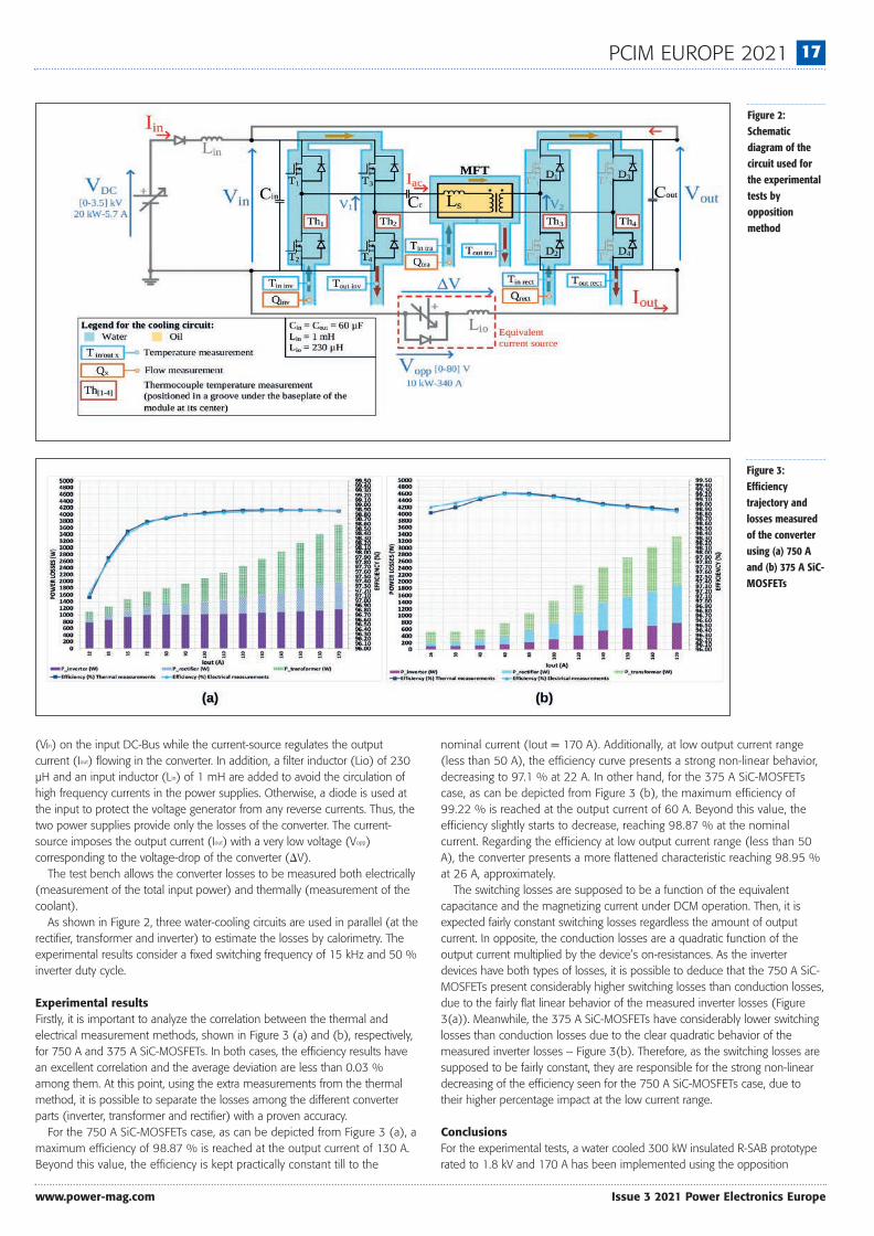
PCIM EUROPE 2021 17
www.power-mag.com Issue 3 2021 Power Electronics Europe
(Vin) on the input DC-Bus while the current-source regulates the output current (Iout) flowing in the converter. In addition, a filter inductor (Lio) of 230 µH and an input inductor (Lin) of 1 mH are added to avoid the circulation of high frequency currents in the power supplies. Otherwise, a diode is used at the input to protect the voltage generator from any reverse currents. Thus, the two power supplies provide only the losses of the converter. The current-source imposes the output current (Iout) with a very low voltage (Vopp) corresponding to the voltage-drop of the converter (�V).
The test bench allows the converter losses to be measured both electrically (measurement of the total input power) and thermally (measurement of the coolant).
As shown in Figure 2, three water-cooling circuits are used in parallel (at the rectifier, transformer and inverter) to estimate the losses by calorimetry. The experimental results consider a fixed switching frequency of 15 kHz and 50 % inverter duty cycle.
Experimental results Firstly, it is important to analyze the correlation between the thermal and electrical measurement methods, shown in Figure 3 (a) and (b), respectively, for 750 A and 375 A SiC-MOSFETs. In both cases, the efficiency results have an excellent correlation and the average deviation are less than 0.03 % among them. At this point, using the extra measurements from the thermal method, it is possible to separate the losses among the different converter parts (inverter, transformer and rectifier) with a proven accuracy.
For the 750 A SiC-MOSFETs case, as can be depicted from Figure 3 (a), a maximum efficiency of 98.87 % is reached at the output current of 130 A. Beyond this value, the efficiency is kept practically constant till to the
nominal current (Iout = 170 A). Additionally, at low output current range (less than 50 A), the efficiency curve presents a strong non-linear behavior, decreasing to 97.1 % at 22 A. In other hand, for the 375 A SiC-MOSFETs case, as can be depicted from Figure 3 (b), the maximum efficiency of 99.22 % is reached at the output current of 60 A. Beyond this value, the efficiency slightly starts to decrease, reaching 98.87 % at the nominal current. Regarding the efficiency at low output current range (less than 50 A), the converter presents a more flattened characteristic reaching 98.95 % at 26 A, approximately.
The switching losses are supposed to be a function of the equivalent capacitance and the magnetizing current under DCM operation. Then, it is expected fairly constant switching losses regardless the amount of output current. In opposite, the conduction losses are a quadratic function of the output current multiplied by the device’s on-resistances. As the inverter devices have both types of losses, it is possible to deduce that the 750 A SiC-MOSFETs present considerably higher switching losses than conduction losses, due to the fairly flat linear behavior of the measured inverter losses (Figure 3(a)). Meanwhile, the 375 A SiC-MOSFETs have considerably lower switching losses than conduction losses due to the clear quadratic behavior of the measured inverter losses – Figure 3(b). Therefore, as the switching losses are supposed to be fairly constant, they are responsible for the strong non-linear decreasing of the efficiency seen for the 750 A SiC-MOSFETs case, due to their higher percentage impact at the low current range.
Conclusions For the experimental tests, a water cooled 300 kW insulated R-SAB prototype rated to 1.8 kV and 170 A has been implemented using the opposition
Figure 2: Schematic diagram of the circuit used for the experimental tests by opposition method
Figure 3: Efficiency trajectory and losses measured of the converter using (a) 750 A and (b) 375 A SiC-MOSFETs
PCIM21.qxp_Layout 1 24/06/2021 13:47 Page 17

18 PCIM EUROPE 2021
Issue 3 2021 Power Electronics Europe www.power-mag.com
method and two different ways for computing the losses: electrical and calorimetric methods. The efficiency was measured for a switching frequency of 15 kHz and considering three different SiC power modules. Regarding the use of 750 A SiC-MOSFET devices, maximum and nominal efficiency of 98.87 % have been achieved. By replacing them with 375 A SiC-MOSFET devices, the converter reached a maximum efficiency of 99.22 % and a nominal efficiency of 98.87 %. On the one hand, the low voltage switching has been improved, while on the other hand, the conduction losses have increased, thus counteracting the effect of output capacitance reduction.
Nevertheless, by using full SiC-Diode modules in the output rectifier, this issue has been diminished, resulting in a maximum efficiency of 99.33 % and
a nominal efficiency of 99.02%. Overall, these results show that an experimental test bench, rated for full
power, is essential, mainly, considering the power, voltage and switching frequency levels required by this project. Finally, the proper understanding of switching waveforms and choice of semiconductors devices regarding the output capacitance are inevitably necessary to achieve such outstanding converter efficiency.
Literature Characterization of a 300 kW Isolated DC-DC Converter using 3.3 kV SiC-MOSFETs, Proceedings PCIM Europe digital days 2021, pages 745-750
Adaptive Current Source Gate Driver for SiC MOSFETs This awarded paper (Young Engineer Award) presents the design and operating principles of a novel current-source gate driver for SiC MOSFETs with adaptive functionalities that aims to improve controllability of di/dt and dv/dt compared to conventional totem-pole voltage source gate drivers. The proposed gate driver is capable of providing a double injection of the gate current. Gard Lyng Rødal, Norwegian University of Science and Technology (NTNU), Norway ([email protected]) The manufacturers of SiC MOSFETs usually recommend a negative drive voltage for turn-off (e.g., -5 to -8 V), and hence a larger voltage difference must be overcome to reach the threshold voltage of the switch, which increases turn-on delay times. However, the existing CSGD (current-source gate drivers) designs lacks the ability of providing further current pulses to further adjust the switching waveforms. For instance, when the MOSFETs reach the Miller plateau, the gate current is generally clamped at some value, with little ability to further alter the switching behavior of the device.
A current source driver that aims to increase the switching speed and enhance dv/dt and di/dt controllability of SiC MOSFET by injecting two pulses of gate current at specified time intervals during turn-on and turn-off switching transients has been designed. The first current injection
aims at reducing the turn-on delay time and provide current until the gate-source voltage reaches a specific value (e.g. the Miller plateau voltage). The second current injection aims to adjust the time the gate-source voltage is clamped at the Miller plateau, by either sourcing or sinking additional gate current at this stage. Thus, the proposed driver takes advantage of the voltage dependent capacitances governing the switching transients of SiC MOSFETS, to adjust and shape the turn-on/off delay times, di/dt and dv/dt of the switched device.
Driver concept The schematic (Figure 1) of the proposed adaptive CSGD comprises a full-bridge circuit (T1 � T4) with three charging inductors LM, LH and LL. One additional auxiliary switch (Taux) is connected in parallel to the driving voltage source. The driving voltage sources are VH for the on-state gate voltage and VL
for off-state voltage. Two bias capacitors CbH and CbL are paralleled to the voltage sources to provide gate charge at the switching transients.
The turn-on process is initiated by pre-charging the inductor LM to the defined current value. This is done by keeping the switches T1 and T4 in the on-state, which cause the charging of the inductor. After pre-charging LM, the MOSFET is turned on by injecting im into the gate. By turning T4 off while keeping T1 on, im is commutated into the gate path. After turn-on, the second
Figure 1: Schematic diagram of the proposed adaptive CSGD (ACSGD) and the SiC MOSFET under test (DUT)
PCIM21.qxp_Layout 1 24/06/2021 13:47 Page 18

www.pcim.mesago.com PCIM EUROPE 2021 19
www.power-mag.com Issue 3 2021 Power Electronics Europe
current injection is prepared by turning Taux on. Both the value of iaux and the timing of when to push the current to the gate
is decided by the on duration of Taux together with the turn-on/off instants of
the switches T1, T3 and Taux. Thus, by adjusting the value of taux, the magnitude of iaux and the current injection instant are configurable. This auxiliary current injection allows for a second adjustment of the gate voltage; hence a finer control of the drain-source voltage rise and fall times of the DUT and a faster/slower transition through the Miller plateau is achievable. The auxiliary turn-on completes the turn-on process with the gate voltage to be kept constant at VH by keeping T3 on. The complete waveform of the turn-on process is shown in Figure 2.
The gate-source manipulation achieved by the proposed ACSGD allows for separate control of turn-on/off delay times, di/dt and dv/dt, as well as for reduced switching loss of the device under test. The working principle is verified experimentally using a passive capacitive load imitating the input-capacitance Ciss of the DUT. It has been shown experimentally that Vgs can be accurately manipulated by varying the timing parameters of the drive switches. A reduction of the ?????? rise time can be reduced by 40 % and manipulated with a second current injection.
Literature An Adaptive Current Source Gate Driver for SiC MOSFETs with Double Gate Current Injection, Proceedings PCIM Europe digital days 2021, pages 1271-1277
LEFT Figure 2: Waveforms of the complete turn-on sequence
This awarded paper (Young Engineer Award) focuses on the high cycle fatigue zone with low temperature swings for power modules, which is a new field in experimental testing. An advanced power cycling test concept, which can provide switching and conduction losses, was used. This combination allows accelerated testing with a load frequency of 50 Hz while avoiding to over-stress devices with a current beyond specification. A design of experiments was developed and carried out with several million power cycling swings. Unexpectedly, the results can be fitted with standard models up to temperature swings 25 K. A wide range of simulations has been performed to further investigate the temperature distribution and the mechanical background. The mechanical simulation underlined the failure analysis which exposes solder layer degradation as a main failure mode for low temperature swings. Christian Schwabe, Technische Universität Chemnitz, Germany ([email protected])
For standard packaging technology, bond wires and solder layers are the main weak points. For these kinds of failure positions empirical lifetime models,
based on a high number of samples, have been introduced. For small temperature swings, experimental data is very rare. Lifetime statistics in this range are hard to obtain, because for these test conditions a long runtime up to several years is expected. To reduce testing time, the on-time is reduced in the millisecond range. This leads to new challenges, because to generate enough losses for a suitable accelerated test, higher currents than the rated current have to be used. To circumvent this disadvantage, a new test concept was developed.
Power cycling with switching losses A new test strategy based on standard power cycling topology but with a special pulse pattern was developed. It can combine the advantage of an adjustable portion of switching losses and high measurement accuracy (Figure 1).
A total of three devices can be tested per phase: two devices with switching losses (DUT 1, 2) and one device with only conduction losses as reference device. The reference device is subjected to a standard power cycling test (DC-test). The load current is toggled with high frequency between the switched devices. This leads to inductive switching where the voltage is limited by a boosted active clamping circuit (BAC). A single turn-off event is shown in
Power Cycling Lifetime Investigation
Figure 1: Schematic circuit of power cycling switching losses with detailed phase 1 Figure 2: Single turn-off event for load current of 150 A and 250 V collector-emitter voltage
PCIM21.qxp_Layout 1 24/06/2021 13:47 Page 19

20 PCIM EUROPE 2021 www.pcim.mesago.com
Issue 3 2021 Power Electronics Europe www.power-mag.com
Figure 2. With this test concept it is possible to generate additional switching losses depending on the switching frequency and switching inductance Lx.
In the experimental section, a total of six tests have been performed with the same Econo-style package module type. The design of experiment was carried out in a way that the first results in test 1-3 can be compared directly with standard power cycling methods due to the temperature swing up to 50 K. Nevertheless, an extreme low on-time of 10 - 20 ms is used. These test conditions were chosen because of the periodic heating, e.g. in an inverter or rectifier, which correlates with the grid frequency. For 50 Hz in a one-phase system, approx. 10 ms heating time occurs, for three phase motor drive systems this can be higher or lower. The time 10 - 20 ms was selected as compromise. The power loss density is still significantly above application level to ensure accelerated testing.
For the 50 Hz half-sine application with an expected Zth,j-c (0,01s) = 0.05 K/W the worst-case temperature ripple is in the range of 13 K which leads to a
PV/A of 2.5 W/mm2. The test results and the failure analysis showed that the failure mode for
test 1 (DC-test) is bond wire lift-off (+5% Vce). This was expected due to the high load current which was approx. 1.8 times the rated current. Test 2 and 3 show a mix between +5% Vce and +20 % Rth increase. While test 2 shows a tendency to bond wire lift off, test 3 tends more towards solder layer degradation (+20% Rth). Test 4 and 5 clearly fail by solder layer degradation with a still good bond wire health state.
The finished experimental results after a total of more than 250 million power cycling swings for tests 1-5 are shown in Figures 3 and 4.
Literature Power Cycling Lifetime Investigation under Low Temperature Swings and 50 Hz Load with Experiment and Simulation, Proceedings PCIM Europe digital days 2021, pages 1377-1384
Figure 3: Experimental results for test 1 and 3 with CIPS reference expectation in black and modified CIPS in red for ton = 20 ms
Figure 4: Experimental results for test 2, 4 and 5 with CIPS reference expectation in black and modified CIPS in red for ton = 10 ms
This awarded paper (Young Engineer Award) proposes power cycling tests of engineering samples with highly reliable chip-near interconnects and commercial modules with standard interconnects for reference. The results reveal a high power cycling capability of the engineering samples - roughly ten times higher than the power cycling capability of the reference modules - which motivates to identify approaches to accelerate the EOL tests. Such an approach has been investigated by power cycling under thermal over-load conditions in combination with short load pulses, permitting to reduce the test time of chip-near interconnects from several months to one day without changing the underlying failure mechanism. Thus, the proposed approach is suitable to reduce qualification costs and time-to-market of new products and innovations drastically. Carsten Kempiak, Otto-von-Guericke-University Magdeburg, Germany ([email protected])
Recent highly reliable interconnect technologies like silver sintering, diffusion soldering and copper bond wires are increasingly used in power semiconductor devices. They permit to achieve a higher reliability or to operate the devices at elevated junction temperature, either resulting in a higher power density or permitting operation in harsh environments with elevated temperature. Therefore, advancing the established package qualification tests like power cycling to speed up the qualification process is highly desirable.
Power cycling under thermal overload Lifetime models reveal that the lifetime of power electronic packages depends on many parameters, where the junction temperature swing has by far the
biggest impact. Therefore, performing power cycling tests under thermal overload conditions to further increase the temperature swing is a promising approach to shorten the test time.
For this investigation, special engineering samples with a 650 V/200 A Si IGBT in a standard housing have been built (Figure 1). The bottom side of the IGBT is sintered onto a DCB while a copper bondbuffer is sintered on its top-side, carrying eight thick copper bond wires for the emitter connection. The IGBT is rated for a maximum junction temperature of 175°C. For reference purposes, commercial modules with a similar rating (FS200R07N3E4R) and standard interconnects (thick aluminum bond wires and soldered chips) were additionally tested.
Exemplary power cycling results under thermal overload condition with ∅Tvj = 170 K and with a common test acceleration ∅Tvj = 90 K are shown in Figure 2a for the engineering samples and in 2b for the reference modules, respectively. All of these power cycling tests were carried out at a medium junction temperature of Tvj,m = 120°C and with short load pulses of ton = 0.5 s and toff = 1.5 s. In order to observe whether the underlying degradation process has changed due to the thermal overload condition, the normalized power cycling data of each DUT is plotted together.
For the engineering samples, the +5% VCE,sat failure criterion is always met first due to a continuous increase, indicating continuously growing cracks in the top-side Al-metallisation, as intended to trigger in all test runs. Also the Rthj,c data look quite similar even considering the large difference in the number of cycles to failure Nf : Rthj,c stays roughly constant until the failure threshold is met and starts to increase afterwards, indicating additional
Accelerated Qualification of Highly Reliable Chip Interconnections
PCIM21.qxp_Layout 1 24/06/2021 13:47 Page 20

www.pcim.mesago.com PCIM EUROPE 2021 21
www.power-mag.com Issue 3 2021 Power Electronics Europe
degradations in the thermal path, which are more pronounced at higher ∅Tvj.
The reference modules reveal a different behavior: At common test accelerations, overlapping degradation mechanisms on the chip’s top- and bottom-side occur, yielding an increase of Rthj,c and VCE,sat as well as of ∅Tvj, where the failure threshold of +5% VCE,sat is met due to a typical jump in VCE,sat, indicating a bond wire lift-off.
Obviously, the fast power cycling tests under thermal over-load conditions reduce the test time drastically. In case of the engineering samples, the measured power cycling data derived for different temperature swings look qualitatively similar to Figure 2a for all test runs. Therefore, the same dominating failure mechanism can be expected. Micrographic analyses confirm that the intended failure mechanism has been triggered during power cycling.
In Figure 3 the micrographic analysis of the engineering sample tested under thermal overload of Figure 2a is shown: At the chip edge (Figure 3a), the top-side Al-metallisation is clearly degraded, which was intended to trigger, while the sinter layer underneath the IGBT is not damaged. At the chip centre (Figure 3b), the Al-metallisation as well as the sinter layer is degraded. The latter, however, was triggered after the EOL criterion of +5% VCE,sat was reached (Figure 2a). The dominant failure mechanism is therefore clearly the degradation of the top-side Al-metallisation, which is more pronounced at the chip edge.
Outlook
Packaging technology becomes an even more important topic regarding wide bandgap semiconductors. To benefit from their potential, e.g. the higher switching speeds and higher possible operating temperatures on system level, low-inductive and highly reliable packages are needed. Regarding SiC MOSFETs, the much higher stiffness further challenges the chip-near interconnects, as more plastic strain is generated compared to Si during power cycling. The development of further improvements and new interconnects will obviously be accelerated with the possibility to apply rapid test- and qualification approaches. Consequently, it is aimed to extend the proposed approach for the application to SiC MOSFETs.
Literature Accelerated Qualification of Highly Reliable Chip Interconnect Technology by Power Cycling Under Thermal Overload, Proceedings PCIM Europe digital days 2021, pages 1385-1392
Figure 1: Device under test: 650 V/200 A IGBT in a standard housing with copper baseplate; the highly reliable chip-near interconnect technology is highlighted
Figure 3: Micrographic analysis of an engineering sample after power cycling under thermal overload; ∅Tvj = 170 K; Tvj,m = 120°C
Figure 2: Comparison of the derived normalized power cycling data obtained under thermal overload at ∅Tvj = 170 K and a common test acceleration at ∅Tvj = 90 K for the engineering samples and the reference modules with standard
PCIM21.qxp_Layout 1 24/06/2021 13:47 Page 21

22 POWER SEMICONDUCTORS www.infineon.com/coolsic-mosfet-discretes
Issue 3 2021 Power Electronics Europe www.power-mag.com
As the supply paradigm shifts towards renewables, traditional generation from carbon-based fuels reduces, but also interacts to its advantage by using distributed storage to feed AC back into the grid through inverters for ‘peak-shaving’, to make generation more cost effective and reliable.
To achieve this, batteries need to be able to charge from a cheap or convenient energy source and then discharge to a local load or back into the utility grid as ‘feed in’. AC/DC chargers and DC/AC inverters are established products, but if they can be efficiently combined, then there are costs to be saved. As a result, there is intense interest in ‘bi-directional converters’, with the volume market set to be in households with a local renewable energy source and storage, which may be an EV battery.
Bi-directional converter requirements A major concern is to maximize the energy from solar or wind sources, therefore any losses in electronic power conversion stages must be kept to a minimum, not
least to shorten payback time for the capital costs involved. This has always been true for power processing in any application, so over the years, conversion topologies have evolved towards better efficiency, with 99 % or more now realistic for single stages. For bi-directional converters however, high efficiency has to be maintained with forward and reverse energy flow, which is an added complication. Fortunately, one of the enablers for better efficiency also facilitates bi-directional flow - the use of MOSFETs as synchronous rectifiers in ‘third quadrant’ operation. A typical bi-directional converter outline that might be used as a battery charger and feed-in inverter is shown in outline in Figure 1. The symmetry of the circuit is evident with bridges of MOSFETs able to act as rectifiers, an inverter or DC/DC converter dependent on drive arrangements.
AC/DC stages must also feature power factor correction (PFC) and this is best achieved at medium power levels by the bi-directional ‘totem-pole PFC’ topology where MOSFETs double as line AC
rectifiers and boost switches in AC/DC mode and inverter switches in DC/AC mode. This characteristic of a MOSFET to change function hinges on its ability to not only conduct through its channel in the ‘normal’ direction from drain to source but also in reverse from source to drain with low loss, all under the control of the gate drive. MOSFETs also however feature a parasitic body diode from drain to source which can be an advantage; some circuits that require reverse conduction naturally ‘commutate’ to forward bias this diode to pass energy to the output at the appropriate stage of the switching cycle. The diode is not ideal however and, when conducting, stores significant charge in its junction which is released when reverse biased during each cycle. This results in ‘recovery current’ which causes losses, reducing efficiency, and increased EMI. The diode also has a high forward voltage drop compared with a Silicon rectifier which causes extra dissipation. Turning on the MOSFET channel bypasses the diode so if this is done with little delay, after the complementary MOSFET in the leg of a
Benefits of CoolSiC MOSFETs in Bi-Directional Inverter Applications With the move to renewable energy, there is an increased focus not only on generation but also storage, to make the most of the intermittent supply from wind and solar. Batteries are the common solution and costs are dropping, driven by the technology improvements stemming from the EV market. This opens up opportunities for energy storage at any scale, from domestic to utility. David Meneses Herrera, Senior Staff Application Engineer; and Nico Fontana, Senior Staff Product Definition Engineer, Infineon Technologies
Figure 1: MOSFETs in bridge arrangements suit bi-directional power converters
Infineon_coverqxp.qxp_Layout 1 24/06/2021 14:16 Page 22

www.infineon.com/coolsic-mosfet-discretes POWER SEMICONDUCTORS 23
www.power-mag.com Issue 3 2021 Power Electronics Europe
bridge is turned off, the additional dissipation from the forward conduction of the diode can be minimized.
Bi-directional converters such as the PSFB or versions of the ‘LLC’ arrangement operate with zero voltage switching (ZVS) for highest efficiency, in which mode the reverse recovery of the body diodes is not critical, as the applied reverse voltage rises resonantly. However, there are situations where the converter may transiently enter a ‘hard’ switching mode such as on start-up, shut-down or with load steps, during which periods high voltage is present during recovery, leading to possibly damaging stress. Device failure can also result if recovery is not complete during the on-period of the associated MOSFET channel.
Problems can also occur if the MOSFET switch in a bi-directional converter has too high output charge, QOSS. In a hard-switched converter, the current resulting during switching transitions circulates within the primary circuit of a converter causing losses. The output capacitance Coss also varies strongly with drain-source voltage resulting in high Qoss. If it is the dominant charge to be removed in a soft-switched resonant converter, then it can be difficult to maintain ZVS and high efficiency under worst case conditions. Minimum dead time between high- and low-side switches must also be increased as a function of Qoss, resulting in a significant duty cycle loss at high switching frequencies. With lower Qoss, the circuit can be ‘tuned’ for better efficiency.
For all these reasons therefore, stable and low output capacitance, low QOSS and minimum body diode reverse recovery energy and time are vital for high efficiency and reliability. In some topologies such as
the totem-pole PFC, which is hard-switching, current Silicon superjunction MOSFET technology yields body diodes which are simply not good enough for a viable circuit.
SiC MOSFETs are a better solution Wide bandgap silicon carbide (SiC) MOSFETs are now mainstream and are used for their better figures-of-merit (FOMs) for efficiency at high frequency, compared with Silicon. They have a range of additional advantages as well, such as inherent high temperature operation, low gate charge, lower increase of on-resistance with temperature, or robustness. Importantly for this discussion, their body diodes have much lower recovery charge, along with output capacitance that varies much less than that of Silicon MOSFETs with drain-source voltage. Additionally, for the same RDSON, a SiC MOSFET has
around one sixth of the QOSS of a Silicon superjunction MOSFET.
As a comparison, we can take a Si-based 600 V CoolMOS™ CFD7 superjunction MOSFET (IPW60R070CFD7) and a CoolSiC™ SiC MOSFET 650 V (IMZA65R048M1H) from Infineon. These are both TO-247 packaged devices with similar voltage and on-resistance ratings at 25°C. The general body diode reverse recovery waveform for both is shown in Figure 2, with total reverse recovery charge noted as QRR. For the CoolMOS™ device, the figure is typically 570 nC and for the CoolSiC™ MOSFET just 125 nC at twice the forward current and 10x the rate of change of current dIF/dt.
Figure 3 shows the variation in output capacitance of the two MOSFET technologies, with a range of CoolSiC devices shown compared with the CoolMOS CFD7 superjunction MOSFET. SiC devices show lower Coss at low voltages, with both types low at high voltages. Note however that the IMZA65R048M1H CoolSiC MOSFET changes by a factor of around ten between saturation and full blocking voltage whereas the superjunction MOSFET changes by a factor of about 8000. Although low Coss is good for low loss from charge and discharge currents, a non-zero value for Coss at high voltages with SiC is helpful – it reduces the need to slow switching speed with a gate resistor, to keep drain-source voltage within recommended derating from its maximum value. Otherwise with Si devices, a higher value resistor is needed to limit peak drain voltage, resulting in less controllability.
Reference design shows high efficiency As a demonstration of the advantages of SiC MOSFETs in a bi-directional converter,
Figure 2: MOSFET body diode reverse recovery waveform. SiC exhibits QRR of about 20 % the value of Si MOSFETs
Figure 3: SiC devices show far less variation in output capacitance with drain voltage
Infineon_coverqxp.qxp_Layout 1 24/06/2021 14:16 Page 23

24 POWER SEMICONDUCTORS www.infineon.com/coolsic-mosfet-discretes
Issue 3 2021 Power Electronics Europe www.power-mag.com
switching frequency. Here there are significant efficiency gains to be had, along with a reduction in size and cost of associated components, particularly magnetics. This can result in significant end-product savings in cost, size and weight, as well as lower energy bills. In bi-directional converters, SiC devices can perform all high voltage switching functions with higher efficiency than traditional solutions and with their superior body diode characteristics, can make hard switching topologies such as the totem-pole PFC viable and cost effective.
Infineon offers a range of CoolSiC™ MOSFETs in discrete and module formats
in ratings from 650 V to 1700 V and with on-resistance down to 2 milliohms. The devices are further complemented by a range of EiceDRIVERTM gate drivers in non-isolated and isolated variants for low- and high-side drives, using Infineon’s coreless transformer technology. For a complete solution, current sensing ICs and microcontrollers for digital control are also available.
Literature
[1] 3300 W CCM bi-directional totem pole with 650 V CoolSiC™ and XMC™ Infineon application note AN_1911_PL52_1912_141352
Infineon has showcased a 3.3 kW totem-pole PFC stage (EVAL_3K3W_TP_PFC_SIC) [1] which achieves 73 W/in3 (4.7 W/cm3) power density with a peak efficiency of 99.1 % at 230 VAC input and 400 VDC output (Figure 4). Efficiency also peaks at over 98.8 % when operating in inverter mode, generating 230 VAC at 50 Hz. The evaluation board features full digital control, implemented with the Infineon XMCTM series microcontroller.
Conclusion SiC MOSFETs are a natural evolution from Si superjunction MOSFETs for applications at medium to high power with high
Figure 4: A high-efficiency bi-directional AC/DC-DC/AC converter using CoolSiC MOSFET technology
Infineon_coverqxp.qxp_Layout 1 24/06/2021 14:16 Page 24
www.apec-conf.org APEC 2021 25
www.power-mag.com Issue 3 2021 Power Electronics Europe
The virtual APEC delivers the same exhibitors in a new format that allows visitors to explore exhibit booths – or microsites – based on own schedule. With the added flexibility, one can explore around hundred microsites at the time that works best, while also communicating with representatives using easy chat tools during live staffed hours throughout the conference week. Since all exhibitors (see listing on APEC’s website) have besides these microsides their own website they are available after APEC 2021 offering their products.
That’s why in this APEC review we do not publish products – these can be found on our website power-mag.com. Instead this review focuses on the conference highlights.
Access to select recorded content, including Technical Sessions, Industry Sessions, and Professional Education Seminars, will be available until July 2021. The technical program includes papers of broad appeal scheduled for oral presentation. The various technical venues cover all areas of technical interest for the practicing power electronics professional. Industry Sessions presents information on current topics in power electronics from sources that would not otherwise present at APEC. The target audience for these sessions is also extended to include system engineers/architects and business-oriented people such as purchasing agents, regulatory agencies, along with other people who support the power electronics industry. The Plenary Session continues the long-standing tradition of addressing issues of immediate and long-term interest to the practicing power electronic engineer. The APEC plenary presentations typically have been from invited distinguished professionals.
Plenary sessions This year’s lineup includes distinguished invited professionals who will share their thoughts on six topics, ranging from automotive and wide bandgap technologies to energy storage and the future of power passives. Content will be presented live and will be recorded.
The presentations started with Auxiliary Automotive Drives Revolutionized by Power Electronics given by Annette Muetze, Univ.-Prof. Dr.-Ing from Graz University of Technology in Austria.
While the impact of power electronics on transportation electrification has risen to the foreground on many fronts, the millions of auxiliary drives used in automotive application have continued to remain one of the industry’s best kept secrets hidden under the hood. With more than 100 of such auxiliary drives in typical mid-size and large executive cars, their role in enabling today’s modern car’s performances is of exceptional importance. Given the additional design freedom and performance spaces opened up by the use of power electronics, the number of such small electric drives in automotive applications has at least doubled over the course of the past two
decades. Performance, safety, and comfort related drives become distinguished, and interest has spiked in terms of energy conversion efficiency, size, and cost, as well as when it comes to electromagnetic emission, noise, and fault tolerance. In this talk, it was discussed how these seemingly unnoticed small drives have been completely revolutionized by power electronics, where the beauty and power often emerge in rediscovering simplicity itself. Some examples explored in this talk include meeting the required EMI standards at reduced component counts, a simple drive re-design that can be considered during manufacturing that reduces the generated noise, as well as increasing drive efficiency by reducing the control to its essence. One of her remarks regarding “Switched Reluctance Motors” in these applications: not of interest.
Edoardo Merli, Power Transistor Macro-Division General Manager and Group Vice President at STMicroelectronics talked about Wide Bandgap Technologies: Enabling a Broader Power Application Domain.
Physical limits prevent current Silicon technology from achieving the greater power density and miniaturization the market needs from power products to meet growing environmental concerns. As an alternative, wide-bandgap (WBG) power products are gaining traction in the market because of their energy efficiency and because they help address many of those environmental issues. For example, SiC and GaN WBG materials, which enable superior overall performance, are helping manufacturers attain remarkable gains in applications like traction inverter for SiC and adaptors/chargers for GaN. Still, Si products should co-exist with the WBG products owing to their cost-effectiveness in some low-power applications or whenever system performance is deemed adequate.
Stephanie Watts Butler, Texas Instruments; JC-70 Chair; and Peter Friedrichs, Infineon; JC-70.2 Co-Chair; discussed Maturing Wide Bandgap Semiconductors Fosters Standardization (JEDEC JC-70 addresses unique characteristics and behaviors of WBG).
Wide bandgap semiconductors (SiC and GaN) are recognized for their unique ability to improve performance, efficiency, and power density. Their unique traits are also recognized as driving the need for standardization of reliability, characterization, and datasheet specification. The JEDEC JC-70 Committee for Wide Bandgap Power Electronic Conversion Semiconductors is addressing this need. As wide bandgap products ramp in the market place, standards are also being published by JC-70. This keynote explored the wide bandgap specific properties being tackled by JC-70. A deeper analysis into GaN device on-resistance and transient behaviors and SiC device threshold voltage and reverse recovery traits will demonstrate how standards for reliability, characterization, and datasheet parameters should be considered together. Progress in key areas will be scrutinized for their ability to address the most critical needs. The keynote concluded by examining how standards
APEC 2021 Confirms – WBG Moves Towards BreakthroughThe Applied Power Electronics Conference (APEC) is one of the leading conferences for power electronics professionals and focuses on the practical and applied aspects of the power electronics industry. It is not just a designer’s conference, APEC has something of interest for anyone involved in power electronics, according to the organizer. Due to concerns about the well-being of participants and continued global travel restrictions, APEC 2021 has been presented virtually from June 14 – 17 attracting thousands attendees worldwide.
APEC.qxp_Layout 1 24/06/2021 13:33 Page 25

26 APEC 2021 www.apec-conf.org
Issue 3 2021 Power Electronics Europe www.power-mag.com
discussed, including advanced magnetics design and alternatives to the use of conventional magnetic components. One approach is to use high-Q resonators, mechanical or electromagnetic, that have better performance than resonators built from discrete inductors and capacitors, and can be used in both power conversion and wireless power transfer. The future potential and progress to date on these technologies will be reviewed.
Awarded and interesting conference papers On the following pages we have selected and summarized the most interesting papers for our readers. Contact details are provided for convenience.
are being treated internationally and across the entire application ecosystem. The Present and Future of Magnetics and Other Power Passives has
been discussed by Charles R. Sullivan, Professor of Engineering Thayer School of Engineering at Dartmouth.
High switching frequencies in power electronics are motivated by reducing the size, cost and loss of magnetic components. With advances in semiconductor switch technology, higher frequencies are becoming practical, but the typical result is not the ultra-small ultra-efficient magnetics one might hope for: rather, magnetics have become the critical factor limiting power electronics performance. Ways to overcome these limitations will be
High-Density Integrated Power Electronics SiC Building Block Modular, medium-voltage (MV) converters have grown in popularity due to their ability to be scaled to higher voltage and current ratings and reduce production and maintenance costs. The power electronics building block (PEBB) concept was proposed by the Office of Naval Research (ONR) in 1997 as a universal power converter for power systems on ships. Since then, many modular MV converters have been developed using silicon IGBTs and various topologies including as a 3-level NPC and single phase 5-level H-bridge. A half-bridge SiC module prototype is fabricated and tested to provideinsight into the substrate functionality and to aid in the refinement of the iPEBB concept. Narayanan Rajagopal, Virginia Polytechnic Institute & State University ([email protected])
With the advancement of WBG devices like SiC-MOSFETs, a new frontier of
higher density MV power converters have emerged. Some recent demonstrations of such PEBBs include a 100 kW, 28 kHz, hybrid Si-IGBT/SiC-MOSFET three-level T-type PEBB with a power density of 27.7 kW/l; and a 100 kW, 100 kHz SiC H-bridge PEBB with a power density of 5 kW/l (PEBB 1000). It used two commercial 1.7 kV SiC half-bridge modules to form an H-bridge converter. The PEBB 1000 is comprised of many discrete components – SiC half-bridge modules, gate drivers, magnetics, and capacitors. These components are connected using additional mechanical parts, such as screws, busbars, and baseplates. The connection of multiple discrete components limits the volumetric power density, performance, and manufacturability of the PEBB.
The presented design feature a 250 kW, 500 kHz integrated power electronics building block (iPEBB) for high-density applications. Simulation work was performed to design a common substrate that will serve as the electrical, thermal, and mechanical foundation of the iPEBB. SiC MOSFET bare dies and passive components that form the iPEBB topology will be directly placed on the common substrate to provide electrical interconnects and a unified platform for cooling.
Substrate survey To form the common substrate, various ceramic and organic materials were explored such as organic DBC (ODBC). The ODBC in this work uses a thin polyimide film for the dielectric. The ductility of the film enables thick metal layers (>1 mm), compatibility with a variety of conductors (e.g., Cu, Al, TPG), and large footprints (>300 mm by 600 mm), enabling, in theory, the entire iPEBB to be on a single ODBC sheet. This would eliminate the need for a baseplate, especially since the ODBC can achieve thick metallization, which can provide the mechanical support for the iPEBB. Eliminating the baseplate removes a thermal interface, and can simplify manufacturing, reduce weight, and improve reliability.
The ODBC is a promising technology that is compatible with a variety of conductors and comes in thick metallization and large footprints. The thick metallization offers heat spreading and mechanical support for the converter. The ODBC’s large footprint offers the ability to eliminate the need for a baseplate thereby reducing the number of thermal interfaces, reducing the weight below 16 kg, and simplifying the manufacturing process. The common substrate uses a multi-layer ODBC design to provide a common-mode (CM) screen and a low power loop inductance for fast switching application (Figure 1). But the implementation of the common substrate will require trade-offs including increased thermal resistance associated with a multi-layer design.
Switching tests were performed at 1 kV, revealing a dv/dt of 27 V/ns and a voltage overshoot of approximately 96 V. The thermal resistance measurements and simulations confirmed that thicker top-side metallization will be needed for improved heat spreading. These insights will go into a multi-physics redesign of the iPEBB and will advance high density medium-voltage converters for future electric systems.
Literature Design of a High-Density Integrated Power Electronics Building Block (iPEBB) Based on 1.7 kV SiC MOSFETs on a Common Substrate, APEC 2021 Procedings, pages 1-8
Figure 1: (a) Common substrate with the integrated SiC bridges, (b) top view of the integrated SiC bridges, (c) half-bridge schematic, (d) switching cell, (e) cross section of multi-layer OBDC common subtrate
APEC.qxp_Layout 1 24/06/2021 13:33 Page 26
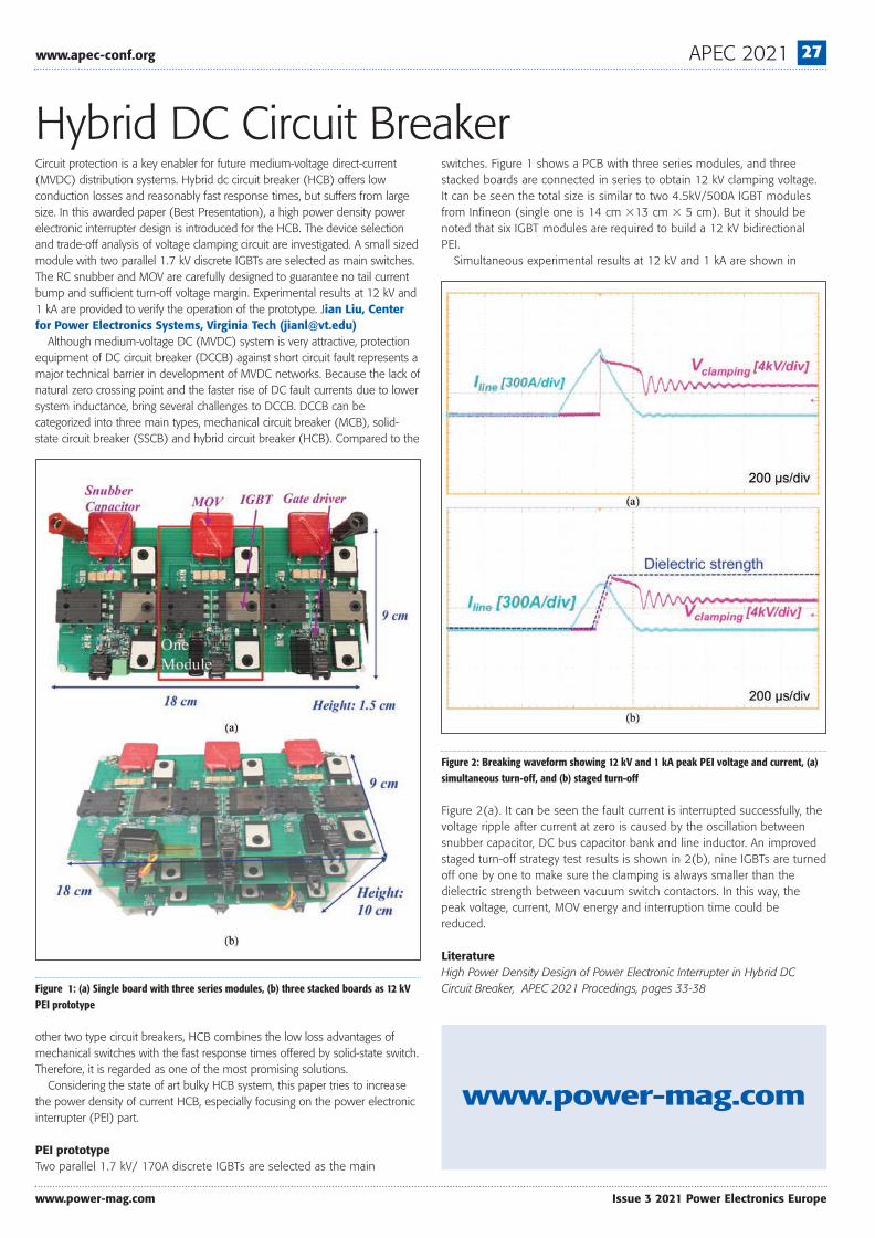
www.apec-conf.org APEC 2021 27
www.power-mag.com Issue 3 2021 Power Electronics Europe
Circuit protection is a key enabler for future medium-voltage direct-current (MVDC) distribution systems. Hybrid dc circuit breaker (HCB) offers low conduction losses and reasonably fast response times, but suffers from large size. In this awarded paper (Best Presentation), a high power density power electronic interrupter design is introduced for the HCB. The device selection and trade-off analysis of voltage clamping circuit are investigated. A small sized module with two parallel 1.7 kV discrete IGBTs are selected as main switches. The RC snubber and MOV are carefully designed to guarantee no tail current bump and sufficient turn-off voltage margin. Experimental results at 12 kV and 1 kA are provided to verify the operation of the prototype. Jian Liu, Center for Power Electronics Systems, Virginia Tech ([email protected])
Although medium-voltage DC (MVDC) system is very attractive, protection equipment of DC circuit breaker (DCCB) against short circuit fault represents a major technical barrier in development of MVDC networks. Because the lack of natural zero crossing point and the faster rise of DC fault currents due to lower system inductance, bring several challenges to DCCB. DCCB can be categorized into three main types, mechanical circuit breaker (MCB), solid-state circuit breaker (SSCB) and hybrid circuit breaker (HCB). Compared to the
switches. Figure 1 shows a PCB with three series modules, and three stacked boards are connected in series to obtain 12 kV clamping voltage. It can be seen the total size is similar to two 4.5kV/500A IGBT modules from Infineon (single one is 14 cm �13 cm � 5 cm). But it should be noted that six IGBT modules are required to build a 12 kV bidirectional PEI.
Simultaneous experimental results at 12 kV and 1 kA are shown in
Hybrid DC Circuit Breaker
Figure 1: (a) Single board with three series modules, (b) three stacked boards as 12 kV PEI prototype
Figure 2: Breaking waveform showing 12 kV and 1 kA peak PEI voltage and current, (a) simultaneous turn-off, and (b) staged turn-off
other two type circuit breakers, HCB combines the low loss advantages of mechanical switches with the fast response times offered by solid-state switch. Therefore, it is regarded as one of the most promising solutions.
Considering the state of art bulky HCB system, this paper tries to increase the power density of current HCB, especially focusing on the power electronic interrupter (PEI) part.
PEI prototype Two parallel 1.7 kV/ 170A discrete IGBTs are selected as the main
Figure 2(a). It can be seen the fault current is interrupted successfully, the voltage ripple after current at zero is caused by the oscillation between snubber capacitor, DC bus capacitor bank and line inductor. An improved staged turn-off strategy test results is shown in 2(b), nine IGBTs are turned off one by one to make sure the clamping is always smaller than the dielectric strength between vacuum switch contactors. In this way, the peak voltage, current, MOV energy and interruption time could be reduced.
Literature High Power Density Design of Power Electronic Interrupter in Hybrid DC Circuit Breaker, APEC 2021 Procedings, pages 33-38
www.power-mag.com
APEC.qxp_Layout 1 24/06/2021 13:33 Page 27

28 APEC 2021 www.apec-conf.org
Issue 3 2021 Power Electronics Europe www.power-mag.com
control of the saturation current while maintaining a competitively low on-resistance.
Experimental results To demonstrate the benefits of the SCCL, a standard GaN device with a GaN device with SCCL has been compared. Both devices have the same chip-area, have the same 650-V rating, and have been packaged in 8x8 mm PQFN. Figure 3 shows the room-temperature output characteristics: when the gate is fully on (Vgs = +12 V), the standard device has an average static Ron of 53 mΩ and a saturation current (Id,sat) that exceeds 120 A, whereas the device with the SCCL has an average static Ron of 71 mΩ and a significantly lower Id,sat of 42 A.
With the SCCL technology, a 3x reduction in Id,sat can be achieved with only a 0.35x increase in static on-resistance. This is possible because the Ron is mostly determined by the GaN-HEMT drain-access region (the equivalent of the “drift region” in a conventional power device), which is not affected by the SCCL blocking area. In fact, to control Id,sat, it is sufficient to deploy the current block only in a small length along the entire source-drain spacing. Although the SCCL device has significantly lower Id,sat than the standard device, the SCCL Id,sat is still
Short-Circuit Capability for GaN Power SwitchesShort-circuit capability is essential for the adoption of GaN power devices. An innovative solution for GaN power switches to achieve short-circuit withstanding time (SCWT) equal to or greater than 3 microseconds with limited increase in on-resistance, has been introduced by Transphorm. Thanks to extended SCWT, the Short-Circuit Current Limiter SCCL technology allows the industry to adopt conventional short-circuit protection schemes, with sufficient immunity to noise and switching transients. Davide Bisi, Transphorm Inc. ([email protected])
In conventional Silicon-based power-devices, the SCWT can be greater than 10 µs. On the other hand, ensuring a high SCWT in WBG devices is more challenging. Due to their own nature and virtue, WBG devices can deliver much higher power density in smaller areas than Silicon devices. Consequently, when subjected to short-circuit conditions, they may experience a steeper rise in temperature resulting in shorter SCWT than Silicon-based counterparts.
Short-circuit current limiter The solution presented is based on the Transphorm normally-off two-chip core technology. A low-voltage normally-off silicon FET is connected in cascode configuration with a high-voltage normally-on GaN HEMT. The Si-FET offers high threshold (+4 V) and highest gate reliability thanks to the robust SiO2/Si MOS technology. The GaN HEMT is fabricated on Silicon substrates for cost-effective manufacturing, and employs a field-plate structure to improve electric-field management and overall reliability. The field-plate is isolated with a dielectric layer to suppress leakage current and off-state losses.
SCCL has been patented for GaN devices (Figure 1). In a two-chip normally-
off solution, lower short-circuit current and higher SCWT can be achieved by controlling either the saturation-current (Id,sat) of the Si-FET or the saturation-current of the GaN-HEMT.
The SCCL was implemented on Transphorm’s core technology by removing segments of the 2DEG channel along the width of the GaN-HEMT by using a proprietary process. The top-view of a standard GaN-HEMT and a GaN-HEMT with SCCL are shown in Figures 2a and b. Longitudinal cross-sections of the SCCL device are shown in Figures 2c and d. The section AA’ is taken along current aperture path, where the 2DEG is uninterrupted from source to drain and electrons can flow in the on-state. In the aperture, the 2DEG properties (charge density & mobility) and the pinch-off voltage of the field-plate structure are the same as the standard device. The section BB’ is taken along current-blocking path, showing the lack of 2DEG under a limited portion of the field-plate structure. The proper design of the current-blocking segmentation (length, width and periodicity of the current block areas) ensures a good
Figure 1: The Short-Circuit Current Limiter (SCCL) acts to reduce the drain-source saturation-current (Id,sat) to increase the SCWT of the device while preserving low on-state resistance
Figure 2: Top-view of two-chip normally-off GaN switch (a) without and (b) with the patented Short-Circuit Current Limiter (SCCL). The SCCL is implemented by removing segments of the 2DEG channel along the width of the GaN HEMT. Longitudinal cross-sections taken along paths featuring (c) the current aperture, and (d) the current block
Figure 3: Room-temperature output curves of (a) standard 650-V GaN device and (b) 650-V GaN device with SCCL. When the gate is fully on (Vgs = +12 V), the standard device has a saturation current (Id,sat) that exceeds 120 A, whereas the device with the SCCL has a significantly lower Id,sat of 42 A. A 3x reduction in Id,sat is achieved. with only a 0.35x increase in on-resistance
APEC.qxp_Layout 1 24/06/2021 13:34 Page 28

www.apec-conf.org APEC 2021 29
www.power-mag.com Issue 3 2021 Power Electronics Europe
more than 2x higher than the maximum rated DC-current (20 A at room temperature). This is important to ensure not only good on-state operations, but also fast switching and fast discharge of the output capacitance (Coss) during turn-on transients. Finally, the SCCL technology does not degrade the quality of the field-plate dielectric isolation, as no increase in 650-V off-state leakage current has been observed with respect to the standard device.
In order to assess the dynamic performance of the SCCL device, dynamic Ron tests and inductive switching tests were carried out with a resistive load of 80 Ω at a DC-bus of 480 V. On-state pulse-width and duty-cycle are 2 µs and 0.01 % respectively. The device remains in the off-state for most of the
Automotive GaN DC/DC Converter To achieve a fast load transient response time in a switching power converter, constant on-time (COT) hysteretic mode control has been reported recently. However, due to the limitations on fixed on-time and mandatory minimum off-time, sluggish response and large voltage over-/undershoot are severe during extreme load transient scenarios. This paper presents a load transient enhance scheme which achieves adaptive on-time (AOT) transient response promptly and within one switching cycle, through instantaneous load change sensing technique. Xugang Ke, Analog Devices Power Products Group ([email protected])
Modern automotive-use application processors (APs) tend to operate with low voltage but high current. With a battery input voltage (VIN) ranging from 3 to 40 V, nominal supply voltage of an AP is only around 1.2V. Wide-input DC/DC conversion is thus essential. For high efficiency and low cost, single-stage implementation is highly preferred. On the other hand, GaN FETs prove to work as better power switches over Silicon MOSFETs, owing to high channel conductivity, low parasitic capacitance and high breakdown voltage.
Single-stage GaN based DC/DC converter Based on the AOT control, a single-stage GaN based DC/DC converter is designed. Because a GaN switch inherently has no body diode and thus shows a high reverse conduction voltage, the efficiency is degraded with excessively long dead time (tdead). Accordingly, a sample-and-hold (S/H) based closed-loop dead time control is proposed to regulate tdead adaptively according to instantaneous input voltage (VIN) and IO (Figure 1). It primarily consists of GaN power switches (MH &ML) and a transient enhanced AOT hysteretic controller. The controller includes a main comparator (CMP) with adaptive slope generator (VSLP), logic control with a load adaptive
transient enhanced TON timer and a sample-and-hold (S/H) based t dead controller.
The converter is implemented using a 0.35-µm high voltage (HV) BCD process, accomplishing the DC/DC voltage conversion from 40 to 1.2V at 5 MHz. In response to load steps between 0.5 A and 10 A, it achieves a 49 mV/29 mV VO undershoot/overshoot within one switching cycle. Thanks to the adaptive dead time control, the efficiency is improved by 4.8 % at light load and 1.5 % at heavy load, respectively, with a peak value of 89.5 %. Figure 2 shows the chip layout. The die size is 1.65 mm? which includes an on-chip bootstrap capacitor (CBST).
Literature An Automotive-Use 5MHz, 40V to 1.2V, Single-Stage AOT GaN DC-DC Converter with One-Cycle Transient Response and Load-Adaptive Dead Time Control, APEC 2021 Procedings, pages 513-516
test time. The dynamic Ron value was recorded after 60 s of operation to ensure the filling of the traps (if any). Results show that the relative increase between dynamic and static Ron is approximately +18 %. This is similar to the relative increase between dynamic and static Ron in standard devices and indicates that the SCCL blocking region does not exacerbate charge-trapping.
Literature Short-Circuit Capability Demonstrated for GaN Power Switches, APEC 2021 Procedings, pages 370-375
Figure 1: Block diagram of the proposed transient enhanced AOT hysteretic converter Figure 2: Chip implementation of the AOT DC/DC converter
APEC.qxp_Layout 1 24/06/2021 13:34 Page 29

30 APEC 2021 www.apec-conf.org
Issue 3 2021 Power Electronics Europe www.power-mag.com
Power consumption of data centers is increasing rapidly over recent years. Recently, 48 V power architecture has attracted more interest in data centers as it offers more efficient architecture. This awarded paper (Best Presentation) focuses on the implementation of the DC/DC stage of the 3 kW power supply unit. Full-bridge regulated LLC converter is designed with a matrix of two transformers. Ahmed Nabih, Center for Power Electronics Systems at Virginia Tech ([email protected]) Resonant converters present an excellent choice for efficient DC/DC converters as they offer soft-switching for both primary and secondary devices.
both primary, secondary, shielding, and inductor winding. The transformer of the 48 V resonant converter is excited with four times higher volt.sec compared to a 12 V converter. This makes the core cross-section area (Ae) is almost 4x higher as well. With increased core size at high frequency, the transformer core exhibits dimensional effects, namely dimensional resonance and skin effect. Moreover, the core eddy loss component tends to increase with increased core size.
Dimensional resonance Any ferrite material has finite permittivity. This means there’s an induced electric field inside the ferrite material. The interaction between electric and magnetic fields tends to redistribute the magnetic field inside the ferrite core following a decaying sinusoidal distribution. If the core thickness is higher than half the wavelength, the magnetic field starts to flow out-of-phase from the excitation current causing drop in core permeability and increased core loss.
Skin effect and eddy loss Any ferrite material has finite conductivity. The source flux induces ac currents flows inside the core. these ac currents are responsible for the eddy loss. These AC currents will also induce eddy fluxes causing the resultant flux to crowd on the surface of the core. The core thickness needs to be smaller than the ferrite skin depth to avoid skin effect. Figure 2 shows a case study on 3 different sample sizes from the same material showing increased core loss density with core size.
The ferrite core material ML91 (from Hitachi) was selected for two reasons: ML91 has the least core loss or least hysteresis loss when measured on a small toroid sample and the least AC conductivity value at 1MHz when measured and compared to other materials.
Experimental results The converter is implemented on 6-layer PCB, 2 oz. Copper, 35 mΩ/600V GaN devices are used for the primary full-bridge, and 4 mΩ/80 V GaN devices are used for the secondary full-bridge rectifiers. Figure 3 shows the implemented PCB including primary and secondary devices and gate drivers and magnetics.
The resonant inductor is designed on UI core with side legs as well and the same thickness as the transformer. The inductor and transformer cores are
High Power Density 1 MHz 3 kW 400 V-48 V LLC Converter
The LLC Resonant converter, along with GaN devices, breaks new grounds to push the switching frequency to much higher frequencies (>1MHz) than those of the traditional pulse width modulation (PWM) converters. This opens opportunities to reduce the converter size and push for higher power density. When the magnetic size is reduced, planar magnetics (PCB winding) become more relevant.
The design of a high-efficiency high power density 1 MHz 3kW full-bridge LLC converter for 48 V front-end power supply a shown in Figure 1 is described in this paper. The converter is designed on 6-layer PCB that includes
Figure 1: Full-bridge LLC resonant converter
Figure 2: Evaluation of core loss density for different core sizes of the same material (DMR51w)
Figure 3: Implemented 1 MHz 3 kW LLC converter
APEC.qxp_Layout 1 24/06/2021 13:34 Page 30

Figure 4: Tested efficiency at 50 V output voltage
www.apec-conf.org APEC 2021 31
www.power-mag.com Issue 3 2021 Power Electronics Europe
integrated into one core. The converter has variable output voltage from 40 V : 60 V to charge the bus battery. Figure 4 shows the converter tested efficiency compared to the first design with four transformers and a round core shape. The proposed core design offers higher light-load efficiency thanks to the reduced core loss at 48 V output.
Literature High Power Density 1 MHz 3 kW 400 V-48 V LLC Converter for Datacenters with improved Core Loss and Termination Loss, APEC 2021 Procedings, pages 304-309
Monolithic Integration of a 5 MHz GaN Half-Bridge in a 200 V GaN-on-SOI ProcessThis awarded paper (Best Presentation) presented key building blocks of a monolithic GaN half-bridge solution - a binary-weighted digitally-controlled segmented gate-driver, offering slew-rate control; a high-voltage floating level-shifter with glitch prevention; and a monolithic half-bridge with integrated fixed-strength gate-drivers. Together, they facilitate on-chip active gate-driving, improving the reliability of GaN power ICs. Wan Lin Jiang, University of Toronto; Herbert De Vleeschouwer, ON Semiconductor, Belgium
GaN’s high dv/dt can be controlled with active gate-drive methods, which has been demonstrated with Si-GaN copackaged designs. However, the limited range of allowable gate-to-source voltage in GaN HEMTs leads to a higher risk of false turn-on and device over-stress, which can be mitigated with integrated gate-drivers.
The lack of p-type HEMTs in most GaN processes prevents direct migration of Si-based gate-driver designs to GaN. Moreover, the level of integration complexity is limited by the process design kits’ lower maturity level and the
limited range of available passive devices and HEMT voltage ratings. On the other hand, gate-drivers with dynamically-programmable strength can limit EMI and operate reliably under different load conditions. Existing solutions for drive-strength control of monolithic GaN drivers have either used off-chip resistors, which are not dynamically controllable, or a dual-current-supply scheme, which is more amenable to analog control. Digital dv/dt control schemes, thus far unexplored in GaN ICs, provide more design flexibility and are less sensitive to process and temperature variations.
GaN-on-SOI process The circuits are functionally demonstrated using three separate ICs fabricated in imec’s 200 V GaN-on-SOI process, shown in Figure 1. A deep trench isolation is used to isolate voltage domains. This process has a design kit for simulation and layout verification. A 200-V, 80-mΩ power e-HEMT with the segmented gate-driver was fabricated in the imec 200 V GaN-on-SOI process.
With 200 V drain-source and 0 V gate-source voltage, the drain leakage current is 59.6 �A, and drops to 1.5 �A for VGS = -1 V. The GaN circuits were simulated using the MVSG-HV model for the HEMTs, producing a maximum dvDS/dt of 112 V/ns at room temperature. A single-die GaN half-bridge IC with an integrated fixed-strength gate-drive scheme is used to achieve fast and oscillation-free VDS switching performance, highlighting the benefits of monolithic integration. Finally, the potential for fast on-chip voltagelevel translation of high-frequency signals
Literature Monolithic Integration of a 5-MHz GaN Half-Bridge in a 200-V GaN-on-SOI Process: Programmable dv/dt Control and Floating High-Voltage Level-Shifter, APEC 2021 Procedings, pages 728-734 Figure 1: Cross-section of imec’s 200 V GaN-on-SOI process
Efficient Single-Phase Nine-Level InverterThe flying capacitor multilevel inverter is achieving highest power densities in recent power electronic devices. These positive results are based on minimal filter volumes due to effective output switching frequencies around hundreds of kilohertz up to several MHz. To achieve these high output frequencies the flying capacitor multilevel topology is crucial in addition with GaN switches. In theoretical calculations efficiencies around 99.4 % should be possible for the overall inverter at these operation conditions. These target efficiencies could not be reached yet in practical prototypes due to high commutation loop
inductances and parasitic capacitances to the midpoint. This paper investigates the theoretical background of these parasitics, their effect on the inverter and presents an improved hardware implementation to verify the theoretical results. Carina Primas, Digital Industries at Siemens AG, Erlangen/Germany ([email protected])
A layout of a three-phase prototype is designed according to the single-phase prototype with 800 kHz switching frequency with no copper surface underneath the switching voltage potentials of the flying capacitors and even
APEC.qxp_Layout 1 24/06/2021 13:34 Page 31
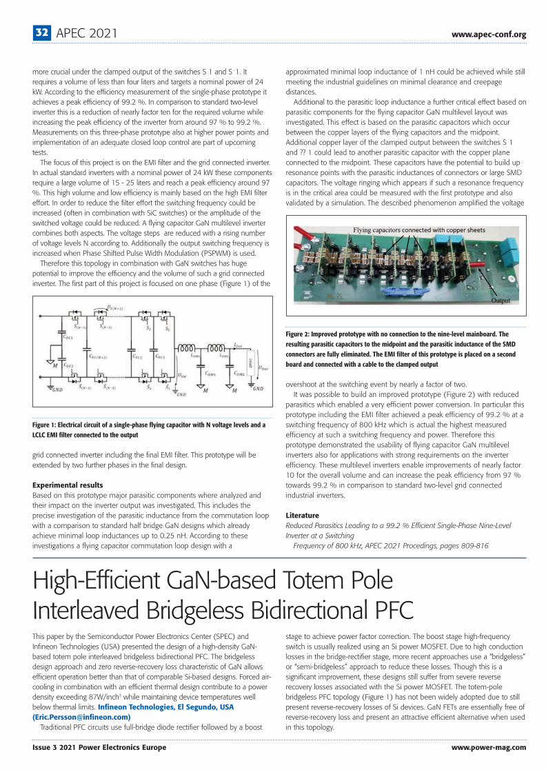
32 APEC 2021 www.apec-conf.org
Issue 3 2021 Power Electronics Europe www.power-mag.com
High-Efficient GaN-based Totem Pole Interleaved Bridgeless Bidirectional PFC
more crucial under the clamped output of the switches S 1 and S�1. It requires a volume of less than four liters and targets a nominal power of 24 kW. According to the efficiency measurement of the single-phase prototype it achieves a peak efficiency of 99.2 %. In comparison to standard two-level inverter this is a reduction of nearly factor ten for the required volume while increasing the peak efficiency of the inverter from around 97 % to 99.2 %. Measurements on this three-phase prototype also at higher power points and implementation of an adequate closed loop control are part of upcoming tests.
The focus of this project is on the EMI filter and the grid connected inverter. In actual standard inverters with a nominal power of 24 kW these components require a large volume of 15 - 25 liters and reach a peak efficiency around 97 %. This high volume and low efficiency is mainly based on the high EMI filter effort. In order to reduce the filter effort the switching frequency could be increased (often in combination with SiC switches) or the amplitude of the switched voltage could be reduced. A flying capacitor GaN multilevel inverter combines both aspects. The voltage steps are reduced with a rising number of voltage levels N according to. Additionally the output switching frequency is increased when Phase Shifted Pulse Width Modulation (PSPWM) is used.
Therefore this topology in combination with GaN switches has huge potential to improve the efficiency and the volume of such a grid connected inverter. The first part of this project is focused on one phase (Figure 1) of the
approximated minimal loop inductance of 1 nH could be achieved while still meeting the industrial guidelines on minimal clearance and creepage distances.
Additional to the parasitic loop inductance a further critical effect based on parasitic components for the flying capacitor GaN multilevel layout was investigated. This effect is based on the parasitic capacitors which occur between the copper layers of the flying capacitors and the midpoint. Additional copper layer of the clamped output between the switches S 1 and ?? 1 could lead to another parasitic capacitor with the copper plane connected to the midpoint. These capacitors have the potential to build up resonance points with the parasitic inductances of connectors or large SMD capacitors. The voltage ringing which appears if such a resonance frequency is in the critical area could be measured with the first prototype and also validated by a simulation. The described phenomenon amplified the voltage
Figure 1: Electrical circuit of a single-phase flying capacitor with N voltage levels and a LCLC EMI filter connected to the output
grid connected inverter including the final EMI filter. This prototype will be extended by two further phases in the final design.
Experimental results Based on this prototype major parasitic components where analyzed and their impact on the inverter output was investigated. This includes the precise investigation of the parasitic inductance from the commutation loop with a comparison to standard half bridge GaN designs which already achieve minimal loop inductances up to 0.25 nH. According to these investigations a flying capacitor commutation loop design with a
overshoot at the switching event by nearly a factor of two. It was possible to build an improved prototype (Figure 2) with reduced
parasitics which enabled a very efficient power conversion. In particular this prototype including the EMI filter achieved a peak efficiency of 99.2 % at a switching frequency of 800 kHz which is actual the highest measured efficiency at such a switching frequency and power. Therefore this prototype demonstrated the usability of flying capacitor GaN multilevel inverters also for applications with strong requirements on the inverter efficiency. These multilevel inverters enable improvements of nearly factor 10 for the overall volume and can increase the peak efficiency from 97 % towards 99.2 % in comparison to standard two-level grid connected industrial inverters.
Literature Reduced Parasitics Leading to a 99.2 % Efficient Single-Phase Nine-Level Inverter at a Switching
Frequency of 800 kHz, APEC 2021 Procedings, pages 809-816
Figure 2: Improved prototype with no connection to the nine-level mainboard. The resulting parasitic capacitors to the midpoint and the parasitic inductance of the SMD connectors are fully eliminated. The EMI filter of this prototype is placed on a second board and connected with a cable to the clamped output
This paper by the Semiconductor Power Electronics Center (SPEC) and Infineon Technologies (USA) presented the design of a high-density GaN-based totem pole interleaved bridgeless bidirectional PFC. The bridgeless design approach and zero reverse-recovery loss characteristic of GaN allows efficient operation better than that of comparable Si-based designs. Forced air-cooling in combination with an efficient thermal design contribute to a power density exceeding 87W/inch3 while maintaining device temperatures well below thermal limits. Infineon Technologies, El Segundo, USA ([email protected])
Traditional PFC circuits use full-bridge diode rectifier followed by a boost
stage to achieve power factor correction. The boost stage high-frequency switch is usually realized using an Si power MOSFET. Due to high conduction losses in the bridge-rectifier stage, more recent approaches use a “bridgeless” or “semi-bridgeless” approach to reduce these losses. Though this is a significant improvement, these designs still suffer from severe reverse recovery losses associated with the Si power MOSFET. The totem-pole bridgeless PFC topology (Figure 1) has not been widely adopted due to still present reverse-recovery losses of Si devices. GaN FETs are essentially free of reverse-recovery loss and present an attractive efficient alternative when used in this topology.
APEC.qxp_Layout 1 24/06/2021 13:34 Page 32

www.apec-conf.org APEC 2021 33
www.power-mag.com Issue 3 2021 Power Electronics Europe
32-phase 1200 A DC/DC Converter for Data Centers
Both high-frequency half-bridges are realized using e-mode GaN HEMTs, specifically 600 V CoolGaN IGO60R070D1.
Converter operation During the positive half-cycle of the AC voltage, S6 is turned on and S5 is turned off. At this time, the half-bridge of phase 1 switches as a boost
active switch and S2 is the synchronous-rectifier switch. The operation of phase 2 is the exact same as that of phase 1, except that
the PWM is shifted 180 degrees with respect to the at of phase 1. This has the effect of reducing the ripple current in both in input and output circuits. Higher efficiency is realized since the output current is split across two paths and can substantially lower I2R losses.
GaN devices are certainly capable of high switching frequencies. However, switching losses in hard-switched continuous conduction mode (CCM) applications such as PFC cannot be neglected. As a compromise between inductor sizing and target efficiency, a switching frequency of 65 kHz is chosen. Almost half the losses of the converter occur in GaN half-bridges (Figure 2).
An efficient thermal design is proposed wherein the top-cooled GaN devices are soldered on PCB cards as half-bridge modules and flank the heatsink on two sides. A third side of the heatsink (the bottom) is used to evacuate heat from Si MOSFETs. Two low power 12V fans are used to remove this heat from the heatsink and provide cooling to the power stage inductors. The complete assembled prototype is shown in Figure 3.
A steady-state thermal model is utilized to predict GaN device junction temperature and provide high overcurrent capability. Experimental results verified a peak efficiency of 99.2 % during DC/DC operation at 2.5 kW and a full-load efficiency of 99.1 % at 5.4 kW.
Literature Design and Implementation of A 5kW 99.2% Efficient High-Density GaN-based Totem Pole
Interleaved Bridgeless Bidirectional PFC, APEC 2021 Procedings, pages 1843-1847
Figure 1: Totem-pole PFC circuit with two high-frequency half-bridges (S1/S2 is the first half-bridge, and S3/S4 is the second)
converter with S2 as the active switch and S1 as the synchronous-rectifier switch. This operation is exactly flipped during the negative half-cycle where S6 is turned on and S5 is turned on. During the negative half-cycle, S1 is the
Figure 2: Loss breakdown at rated power
Figure 3: Assembled 5kW prototype
The paper from presents a multiphase converter solution that provides 1200 A to server and artificial intelligence systems. Computing power in these systems keeps increasing, since CPUs, GPUs, FPGAs and ASICs demand higher and higher current from multiphase interleaved synchronous converters. More than twenty phases of power stage are required, but it is extremely difficult to design a digital PWM controller with more than twenty phases due to limitations in package size and control complexity. Phase paralleling is proposed in this paper to double phase number of a 16-phase digital controller to 32 phases. Wenkang Huang, Infineon Technologies/USA ([email protected]) Computing power of CPUs and GPUs have been increasing steadily to meet demands of data centers, cloud computing, and artificial intelligence systems. Most recently, FPGAs and ASICs have joined forces in artificial intelligence applications and have dramatically boosted computing power. Although output voltage of multiphase synchronous buck converters that power these CPUs, GPUs, FPGAs, and ASICs keeps coming down to as low as 0.6 V to reduce power consumption, the ºrequired converter current has exceeded 1200 A.
Since average current of each phase is usually limited at 40 to 60 A due to restrictions in MOSFET technology and package size, power dissipation, cooling method, and inductor size, more than twenty phases of power stages with current sharing are required to meet this higher current requirement.
Experimental results A 32-phase synchronous buck converter board (Figure 1) was built to demonstrate the 1200 A power solution and accurate current balance during steady-state and dynamic load transient conditions that emulate load current in real data center and artificial intelligence systems.
The board consists of a 16-phase digital controller, 32-phase power stages including inductors, input connectors for input voltage, and on-board electronic loads and output connectors for the 1200 A output current . The board is used to verify the design and evaluate load transient response and current sharing among all the phases.
Current sharing between the sixteen combined phases is realized by the 16-phase PWM controller through average current sharing and dynamic cycle-by-
APEC.qxp_Layout 1 24/06/2021 13:34 Page 33

34 APEC 2021 www.apec-conf.org
Issue 3 2021 Power Electronics Europe www.power-mag.com
cycle current sharing. The average current sharing ensures even thermal distribution, while the fast current sharing in each switching cycle prevents inductor saturation due to high peak current during load transients. The current in each power stage and inductor is not only balanced evenly in steady state but also in dynamic load transient conditions at different load frequencies.
Figure 2(a) and (b) show IMON current waveforms of the three phases with 300 A load step at load frequencies of 10 kHz and 200 kHz respectively. This wide load-frequency range emulates fast and constant load variations in the CPUs, GPUs, FPGAs, and ASICs. Current waveforms of the three phases demonstrate less than 3 A current mismatch between the two paralleled phases during dynamic load changes in wide frequency range.
Literature A 32-phase 1200-Ampere DC/DC Converter for Data Center and Artificial Intelligence Systems, APEC 2021 Procedings, pages 2017-2023
Figure 1: Evaluation board of 32-phase synchronous buck converter
Figure 2: IMON, load current, and PWM waveform of 32-phase converter with 300 A load steps at different load frequencies (a) 10 kHz and (b) 200 kHz
Name:
Company Name:
Address:
Post Code:
Tel: Total Number of Copies @ £ p+p Total £
Drives S & S Hyd H/B Pne H/B Ind Mot CompH/B H/B Air
DFA MEDIA LTD,
QUANTITY QUANTITY
Hydraulics&Pneumatics There are now 6 of these handy
reference books from the publishers ofthe Drives & Controls and
Hydraulics & Pneumatics magazines.
Published in an easily readable styleand designed to help answer basicquestions and everyday problems
without the need to refer to weightytextbooks.
We believe you’ll find them invaluableitems to have within arms reach.
From the publishers of
QUANTITY QUANTITY QUANTITY
If you would like to obtain additional copies of the handbooks, please completethe form below and either fax it on 01732 360034 or post your order to:
Cheques should be made payable to DFA MEDIA LTD and crossed A/C Payee.Copies of the handbooks are available at £4.99 per copy.Discounts are available for multiple copies. 2-5 copies £4.30, 6-20 copies £4.10, 20+ copies £3.75.
QUANTITY
PRACTICAL ENGINEER’S HANDBOOKSPRACTICAL ENGINEER’S HANDBOOKS
HYDRAULICS
INDUSTRIALMOTORS
SERVOSAND STEPPERS
PNEUMATICS
COMPRESSED AIRINDUSTRIAL
ELECTRIC DRIVES
PLEASE ALLOW UPTO 28 DAYS FOR DELIVERY
192 The High Street, Tonbridge, Kent TN9 1BE
Engineers Handbook, DFA MEDIA LTD,192 The High Street, Tonbridge, Kent TN9 1BE
Postage and Packaging:1-3 copies: £2.99 4-6 copies: £4.99 7 or more copies: £6.99
APEC.qxp_Layout 1 24/06/2021 13:34 Page 34

5-7 APRIL 2022 HALLS 9 & 10
NEC BIRMINGHAM
5-7 APRIL 2022HALLS 9 & 10
NEC BIRMINGHAM
BOOK NOW! Contact the team to secure your stand Damien Oxlee +44 (0) 1732 370342 [email protected] Andy Wylie +44 (0) 1732 370341 [email protected]
THE HOME OF AUTOMATION The UK’s leading exhibition for Drives, Automation, Power Transmission and Motion Control Equipment
www.drives-expo.com
IN ASSOCIATION WITH:
CO-LOCATED WITH:
SPONSORS
8 0 % A L R E A D Y S O L D
D&C 2022 A4 Book Now with sponsors.qxp_Layout 1 10/12/2020 14:02 Page 1

You can do more with THA Thinpack on board.
Using the most advanced aluminum electrolytic capacitor technology, type THA and THAS offer the highest energy density in a low profile. Design-in one component versus banks of alternative SMT capacitors for incredible size and cost savings. Improve reliability with one component versus many.
THA: 3,000 hr. life @ 85 ºCTHAS: 3,000 hr. life @ 105 ºC
Replaces banks ofSMT capacitors
Highest energy density inlow-profile: 1.1 J/CC
Uses about 70% less boardspace than alternatives!
For technical information and samples visit cde.com/THA
One Capacitor does the job of many in a fraction of the space.
36_pee_0321.indd 1 25/06/2021 07:16