ISSCC 2015 / SESSION 19 / ADVANCED WIRELESS TECHNIQUES / …
3
342 • 2015 IEEE International Solid-State Circuits Conference ISSCC 2015 / SESSION 19 / ADVANCED WIRELESS TECHNIQUES / 19.1 19.1 Reconfigurable Receiver with >20MHz Bandwidth Self-Interference Cancellation Suitable for FDD, Co-Existence and Full-Duplex Applications Jin Zhou, Tsung-Hao Chuang, Tolga Dinc, Harish Krishnaswamy Columbia University, New York, NY Multiband FDD operation requires numerous off-chip duplexers, which limit form factor. Widely-tunable low-noise RF active self-interference cancellation (SIC) (e.g. [1]) is a step towards enabling duplexers with reduced TX/RX isolation as well as adjacent-channel full duplex. However, SIC bandwidth (BW) is limited to a few MHz due to the selectivity of the high-Q duplexer isolation. Recent works suggest that same-channel full duplex (SC-FD) can greatly improve network performance [2-4]. SIC must be pursued in RF, analog/mixed- signal and digital for SC-FD to achieve the >100dB of SIC required, as filtering the SI is not an option. However, SC-FD self-interference channels can be frequency-selective due to ambient reflections [3], requiring silicon-averse bulky delay lines to replicate the delays in the RF SIC path [2]. In this paper, a 0.8-to-1.4GHz receiver with a tunable, reconfigurable RF SI canceller at the RX input is presented that supports >20MHz cancellation BW across a variety of antenna interfaces (nearly 10× improvement over a conventional canceller). This is accomplished by (i) a bank of tunable, reconfigurable 2 nd -order high-Q RF bandpass filters in the canceller to emulate the antenna interface isolation (essentially RF frequency-domain equalization), and (ii) a linear N-path G m -C filter implementation [5] with embedded variable attenuation and phase shifting. For FDD, SIC enhances effective OOB IIP3 and IIP2 to +25-27dBm and +90dBm respectively. For SC-FD, SIC eliminates RX gain compression for as high as -8dBm of peak in-band SI, and enhances effective in-band IIP3 and IIP2 by 22dB and 58dB. Frequency-domain equalization may be performed by decomposing a signal into sub-bands (analysis) and reconstruction after independent sub-band processing (synthesis). While a conventional flat (broadband relative to the antenna interface) amplitude- and phase-based canceller can only perfectly replicate the isolation at a single frequency point, a 2 nd -order bandpass filter combined with amplitude and phase scaling features four degrees of freedom, namely center-frequency, Q, absolute amplitude and absolute phase. This enables the replication of not just the amplitude and phase of the isolation at a frequency point, but also the slope of the amplitude and the slope of the phase (i.e. group delay), enhancing cancellation bandwidth (Fig. 19.1.1). The group delay of a 2 nd -order bandpass filter is proportional to the Q, and upward/downward shifts of center frequency enable replication of positive/ negative amplitude slopes. The use of a filter bank with independent filter parameters enables such replication at multiple points in different sub-bands, further enhancing cancellation bandwidth (Fig. 19.1.1). Recently, N-path filters have emerged as a promising solution for the implementation of highly-linear high-Q on-chip RF filters [5]. The Q of an N-path filter may be reconfigured via the baseband capacitor (C B ) and the center-frequency may be shifted using clockwise/counter-clockwise-connected baseband G m cells [5]. Interestingly, phase shifting can be embedded in a two-port (input/output) 2 nd -order bandpass N-path filter by phase shifting the LOs driving the switches on the output side (Fig. 19.1.1) – LPTV analysis reveals that this introduces constant phase shifts with no other impact on frequency response. Variable attenuation (amplitude scaling) can be introduced by reconfiguring R RX and R TX relative to each other (Fig. 19.1.1). A second benefit of a frequency-selective canceller is noise-filtering. For FDD, the filter banks are tuned to the TX band. Consequently, the RX band noise of R TX , G m cells and even R RX will be filtered by the low RX-band impedance of the N-path filter. Therefore, RX NF degradation will be lower for FDD than for SC-FD (seen in Figs. 19.1.3 and 19.1.4), although in both cases, degradation is low due to weak RX coupling. Figure 19.1.2 shows the detailed schematic of the receiver. A canceller bank of two 2 nd -order bandpass N-path G m -C filters is implemented, and the filters have separate LO and TX replica signal inputs, lending flexibility in their use (for cancellation of two separate TX signals for MIMO SC-FD applications or for cancellation of TX noise in the RX band). The canceller filters are weakly capacitively coupled to the RX input, with the programmable C C bank chosen to enable -10dB coupling across the operating frequency range. Weak coupling is important in SIC to not degrade RX input matching and NF, and also prevents the interaction of the N-path filters with each other and with the RX. The LO path of each canceller filter includes two vector-interpolation phase shifters with input LO slew-rate-control filters to generate phase-shifted 25% duty-cycle clocks for the output-side switches. Each canceller filter is designed to achieve an attenuation range of 20 to 40dB including the RX-side coupling (enabling support for antenna interface isolations of 30 to 50dB assuming a 10dB coupler on the TX side), full phase-shift range, peak group-delay range of 1 to 28ns for the minimum attenuation setting and peak center-frequency shift of +/-10MHz at the peak group-delay setting. The RX uses a noise-canceling current-mode architecture as in [1]. The input capacitance is resonated using a combination of wirebond and off-chip inductance in the CG-stage to ground and supply. Programmable capacitor banks (Cm) are included to tune the input match to the desired frequency. The prototype 65nm CMOS receiver (Fig. 19.1.7) operates over 0.8 to 1.4GHz, with measured NF of 4.8dB, out-of-band (OOB) IIP3 of +17dBm, OOB IIP2 of +61dBm and OOB blocker P 1dB of +4dBm. For FDD (Fig. 19.1.3), the SI canceller enables the usage of a relaxed, custom-designed LTE-like 0.8GHz/0.9GHz duplexer employing surface-mount-device (SMD)-based 2 nd -order LC filters with 3.2dB/2.7dB TX/RX insertion loss, 115MHz TX/RX separation and only 30dB peak isolation. Despite the duplexer isolation’s peak group delay of 11ns and 7dB amplitude variation across the TX band, the SI canceller achieves a 20dB cancellation BW of 17/24MHz for one/two filters enabled (an increase of 6×/8× over a conventional canceller). The associated NF increase is only 0.5dB/0.6dB due to noise filtering. SIC of up to -4dBm of peak OOB TX leakage at the RX input is demonstrated, and enhances the receiver effective OOB IIP3 from +17dBm to +25 to +27dBm from cross-modulation (triple-beat) measurements and effective OOB IIP2 from +61dBm to +90dBm. To be fair, we ensure that the two-tone TX signal undergoes a cancellation of not more than 25dB (the average cancellation over the 24MHz 20dB SIC BW). In conjunction with advances in SMD inductors and variable capacitors, the proposed wideband SI canceller can enable tunable/low-cost/small-form-factor SMD-based duplexers for FDD. For SC-FD (Fig. 19.1.4), the SI canceller achieves a 20dB cancellation BW of 15/25MHz (one/two filters) across a 1.4GHz narrowband antenna-pair interface with peak isolation group delay of 8ns and peak isolation magnitude of 34dB (an increase of 5×/8× over a conventional canceller). Antenna isolation >30dB is achieved through physical separation here, but can also be obtained through antenna cancellation in practice [3]. The associated NF increase is (0.9 to 1.2)dB/(1.1 to 1.5)dB. SIC of up to -8dBm of peak in-band TX leakage at the RX input results in negligible gain compression of a desired signal (as opposed to nearly 22dB of compression in the absence of SIC). SIC also improves the impact of receiver nonlinearity on the TX leakage itself, improving effective in-band IIP3 from -20dBm to +2dBm and effective in-band IIP2 from +10dBm to +68dBm. Note that additional cancellation to achieve >100dB SIC as well as cancellation of intermodulation products generated by the RX or canceller on the SI can be achieved in digital, but distortion of the unknown desired signal (e.g. gain compression and associated NF increase) cannot be cancelled. Figure 19.1.5 depicts the SC-FD SIC of a 1.37GHz 27MHz-BW RRC-filtered 64-QAM signal across the antenna pair, and 20dB cancellation is observed. TX LO feedthrough to the RX input is ~-55dBm, low enough to not affect FDD/SC-FD operation. Calibration/cancellation techniques can further suppress the TX LO. When compared with prior art (Fig. 19.1.6), this work achieves superior SIC BW, while achieving comparable SI power handling, NF degradation and linearity enhancement under FDD SIC to [1] and supporting SC-FD. Canceller DC power depends on antenna interface selectivity and desired SIC BW, and must be compared with the TX power consumption, as it can be powered down when the TX is inactive, or in the absence of a CW jammer for FDD. References: [1] J. Zhou et al, “A Blocker-Resilient Wideband Receiver with Low-Noise Active Two-Point Cancellation of >0dBm TX Leakage and TX Noise in RX Band for FDD/Co-Existence,” ISSCC Dig. Tech. Papers, pp. 352-353, Feb. 2014. [2] D. Bharadia et al, “Full Duplex Radios,” ACM SIGCOMM, pp.375-386, 2013. [3] B. Debaillie et al, “Analog/RF Solutions Enabling Compact Full-duplex Radios,” IEEE JSAC (Early Access Article) DOI: 10.1109/JSAC.2014.2330171. [4] D. Yang et al, “A Widely Tunable Active Duplexing Transceiver with Same- channel Concurrent RX/TX and 30dB RX/TX Isolation,” in IEEE Radio Frequency Integrated Circuits Symp., pp. 321-324, June 2014. [5] M. Darvishi et al, “Widely Tunable 4th Order Switched G m -C Band-Pass Filter Based on N-Path Filters,” IEEE J. Solid-State Circuits, vol. 47, no.12, pp. 3105- 3119, Dec. 2012. [6] T. Zhang et al, “An integrated CMOS passive transmitter leakage suppression technique for FDD Radios,” IEEE Radio Frequency Integrated Circuits Symp., pp. 43-46, June 2014. [7] V. Aparin et al, “An integrated LMS adaptive filter of TX leakage for CDMA receiver front ends,” IEEE J. Solid-State Circuits, vol. 41, no. 5, pp. 1171-1182, May 2006. 978-1-4799-6224-2/15/$31.00 ©2015 IEEE
Transcript of ISSCC 2015 / SESSION 19 / ADVANCED WIRELESS TECHNIQUES / …

342 • 2015 IEEE International Solid-State Circuits Conference
ISSCC 2015 / SESSION 19 / ADVANCED WIRELESS TECHNIQUES / 19.1
19.1 Reconfigurable Receiver with >20MHz Bandwidth Self-Interference Cancellation Suitable for FDD, Co-Existence and Full-Duplex Applications
Jin Zhou, Tsung-Hao Chuang, Tolga Dinc, Harish Krishnaswamy
Columbia University, New York, NY
Multiband FDD operation requires numerous off-chip duplexers, which limitform factor. Widely-tunable low-noise RF active self-interference cancellation(SIC) (e.g. [1]) is a step towards enabling duplexers with reduced TX/RX isolation as well as adjacent-channel full duplex. However, SIC bandwidth (BW)is limited to a few MHz due to the selectivity of the high-Q duplexer isolation.Recent works suggest that same-channel full duplex (SC-FD) can greatlyimprove network performance [2-4]. SIC must be pursued in RF, analog/mixed-signal and digital for SC-FD to achieve the >100dB of SIC required, as filteringthe SI is not an option. However, SC-FD self-interference channels can be frequency-selective due to ambient reflections [3], requiring silicon-averse bulkydelay lines to replicate the delays in the RF SIC path [2].
In this paper, a 0.8-to-1.4GHz receiver with a tunable, reconfigurable RF SI canceller at the RX input is presented that supports >20MHz cancellation BWacross a variety of antenna interfaces (nearly 10× improvement over a conventional canceller). This is accomplished by (i) a bank of tunable, reconfigurable 2nd-order high-Q RF bandpass filters in the canceller to emulatethe antenna interface isolation (essentially RF frequency-domain equalization),and (ii) a linear N-path Gm-C filter implementation [5] with embedded variableattenuation and phase shifting. For FDD, SIC enhances effective OOB IIP3 andIIP2 to +25-27dBm and +90dBm respectively. For SC-FD, SIC eliminates RX gaincompression for as high as -8dBm of peak in-band SI, and enhances effectivein-band IIP3 and IIP2 by 22dB and 58dB.
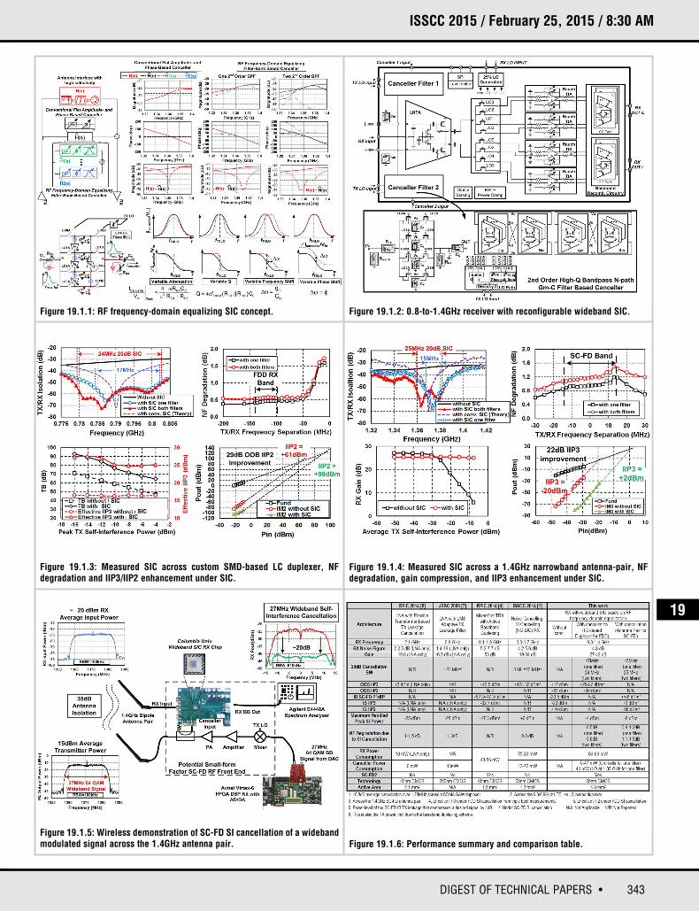
Frequency-domain equalization may be performed by decomposing a signal intosub-bands (analysis) and reconstruction after independent sub-band processing(synthesis). While a conventional flat (broadband relative to the antenna interface) amplitude- and phase-based canceller can only perfectly replicate theisolation at a single frequency point, a 2nd-order bandpass filter combined withamplitude and phase scaling features four degrees of freedom, namely center-frequency, Q, absolute amplitude and absolute phase. This enables thereplication of not just the amplitude and phase of the isolation at a frequencypoint, but also the slope of the amplitude and the slope of the phase (i.e. groupdelay), enhancing cancellation bandwidth (Fig. 19.1.1). The group delay of a 2nd-order bandpass filter is proportional to the Q, and upward/downward shiftsof center frequency enable replication of positive/ negative amplitude slopes. Theuse of a filter bank with independent filter parameters enables such replicationat multiple points in different sub-bands, further enhancing cancellation bandwidth (Fig. 19.1.1). Recently, N-path filters have emerged as a promisingsolution for the implementation of highly-linear high-Q on-chip RF filters [5]. TheQ of an N-path filter may be reconfigured via the baseband capacitor (CB) and thecenter-frequency may be shifted using clockwise/counter-clockwise-connectedbaseband Gm cells [5]. Interestingly, phase shifting can be embedded in a two-port (input/output) 2nd-order bandpass N-path filter by phase shifting theLOs driving the switches on the output side (Fig. 19.1.1) – LPTV analysis revealsthat this introduces constant phase shifts with no other impact on frequencyresponse. Variable attenuation (amplitude scaling) can be introduced by reconfiguring RRX and RTX relative to each other (Fig. 19.1.1). A second benefitof a frequency-selective canceller is noise-filtering. For FDD, the filter banks aretuned to the TX band. Consequently, the RX band noise of RTX, Gm cells and evenRRX will be filtered by the low RX-band impedance of the N-path filter. Therefore,RX NF degradation will be lower for FDD than for SC-FD (seen in Figs. 19.1.3 and19.1.4), although in both cases, degradation is low due to weak RX coupling.
Figure 19.1.2 shows the detailed schematic of the receiver. A canceller bank oftwo 2nd-order bandpass N-path Gm-C filters is implemented, and the filters haveseparate LO and TX replica signal inputs, lending flexibility in their use (for cancellation of two separate TX signals for MIMO SC-FD applications or for cancellation of TX noise in the RX band). The canceller filters are weakly capacitively coupled to the RX input, with the programmable CC bank chosen toenable -10dB coupling across the operating frequency range. Weak coupling isimportant in SIC to not degrade RX input matching and NF, and also preventsthe interaction of the N-path filters with each other and with the RX. The LO pathof each canceller filter includes two vector-interpolation phase shifters with inputLO slew-rate-control filters to generate phase-shifted 25% duty-cycle clocks forthe output-side switches. Each canceller filter is designed to achieve an attenuation range of 20 to 40dB including the RX-side coupling (enabling
support for antenna interface isolations of 30 to 50dB assuming a 10dB coupleron the TX side), full phase-shift range, peak group-delay range of 1 to 28ns forthe minimum attenuation setting and peak center-frequency shift of +/-10MHz atthe peak group-delay setting. The RX uses a noise-canceling current-modearchitecture as in [1]. The input capacitance is resonated using a combination ofwirebond and off-chip inductance in the CG-stage to ground and supply.Programmable capacitor banks (Cm) are included to tune the input match to thedesired frequency.
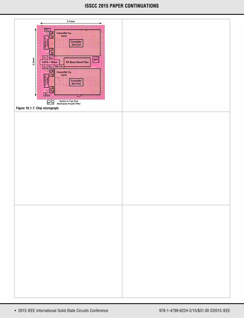
The prototype 65nm CMOS receiver (Fig. 19.1.7) operates over 0.8 to 1.4GHz,with measured NF of 4.8dB, out-of-band (OOB) IIP3 of +17dBm, OOB IIP2 of+61dBm and OOB blocker P1dB of +4dBm. For FDD (Fig. 19.1.3), the SI cancellerenables the usage of a relaxed, custom-designed LTE-like 0.8GHz/0.9GHzduplexer employing surface-mount-device (SMD)-based 2nd-order LC filters with3.2dB/2.7dB TX/RX insertion loss, 115MHz TX/RX separation and only 30dBpeak isolation. Despite the duplexer isolation’s peak group delay of 11ns and7dB amplitude variation across the TX band, the SI canceller achieves a 20dBcancellation BW of 17/24MHz for one/two filters enabled (an increase of 6×/8×over a conventional canceller). The associated NF increase is only 0.5dB/0.6dBdue to noise filtering. SIC of up to -4dBm of peak OOB TX leakage at the RX inputis demonstrated, and enhances the receiver effective OOB IIP3 from +17dBm to+25 to +27dBm from cross-modulation (triple-beat) measurements and effectiveOOB IIP2 from +61dBm to +90dBm. To be fair, we ensure that the two-tone TXsignal undergoes a cancellation of not more than 25dB (the average cancellationover the 24MHz 20dB SIC BW). In conjunction with advances in SMD inductorsand variable capacitors, the proposed wideband SI canceller can enabletunable/low-cost/small-form-factor SMD-based duplexers for FDD.
For SC-FD (Fig. 19.1.4), the SI canceller achieves a 20dB cancellation BW of15/25MHz (one/two filters) across a 1.4GHz narrowband antenna-pair interfacewith peak isolation group delay of 8ns and peak isolation magnitude of 34dB (anincrease of 5×/8× over a conventional canceller). Antenna isolation >30dB isachieved through physical separation here, but can also be obtained throughantenna cancellation in practice [3]. The associated NF increase is (0.9 to1.2)dB/(1.1 to 1.5)dB. SIC of up to -8dBm of peak in-band TX leakage at the RXinput results in negligible gain compression of a desired signal (as opposed tonearly 22dB of compression in the absence of SIC). SIC also improves theimpact of receiver nonlinearity on the TX leakage itself, improving effective in-band IIP3 from -20dBm to +2dBm and effective in-band IIP2 from +10dBm to+68dBm. Note that additional cancellation to achieve >100dB SIC as well as cancellation of intermodulation products generated by the RX or canceller on theSI can be achieved in digital, but distortion of the unknown desired signal (e.g.gain compression and associated NF increase) cannot be cancelled. Figure19.1.5 depicts the SC-FD SIC of a 1.37GHz 27MHz-BW RRC-filtered 64-QAMsignal across the antenna pair, and 20dB cancellation is observed.
TX LO feedthrough to the RX input is ~-55dBm, low enough to not affectFDD/SC-FD operation. Calibration/cancellation techniques can further suppressthe TX LO. When compared with prior art (Fig. 19.1.6), this work achieves superior SIC BW, while achieving comparable SI power handling, NF degradation and linearity enhancement under FDD SIC to [1] and supporting SC-FD. Canceller DC power depends on antenna interface selectivity and desiredSIC BW, and must be compared with the TX power consumption, as it can bepowered down when the TX is inactive, or in the absence of a CW jammer forFDD.
References:[1] J. Zhou et al, “A Blocker-Resilient Wideband Receiver with Low-Noise ActiveTwo-Point Cancellation of >0dBm TX Leakage and TX Noise in RX Band forFDD/Co-Existence,” ISSCC Dig. Tech. Papers, pp. 352-353, Feb. 2014.[2] D. Bharadia et al, “Full Duplex Radios,” ACM SIGCOMM, pp.375-386, 2013.[3] B. Debaillie et al, “Analog/RF Solutions Enabling Compact Full-duplexRadios,” IEEE JSAC (Early Access Article) DOI: 10.1109/JSAC.2014.2330171.[4] D. Yang et al, “A Widely Tunable Active Duplexing Transceiver with Same-channel Concurrent RX/TX and 30dB RX/TX Isolation,” in IEEE Radio FrequencyIntegrated Circuits Symp., pp. 321-324, June 2014.[5] M. Darvishi et al, “Widely Tunable 4th Order Switched Gm-C Band-Pass FilterBased on N-Path Filters,” IEEE J. Solid-State Circuits, vol. 47, no.12, pp. 3105-3119, Dec. 2012.[6] T. Zhang et al, “An integrated CMOS passive transmitter leakage suppressiontechnique for FDD Radios,” IEEE Radio Frequency Integrated Circuits Symp., pp.43-46, June 2014.[7] V. Aparin et al, “An integrated LMS adaptive filter of TX leakage for CDMAreceiver front ends,” IEEE J. Solid-State Circuits, vol. 41, no. 5, pp. 1171-1182,May 2006.
978-1-4799-6224-2/15/$31.00 ©2015 IEEE
343DIGEST OF TECHNICAL PAPERS •
ISSCC 2015 / February 25, 2015 / 8:30 AM
Figure 19.1.1: RF frequency-domain equalizing SIC concept. Figure 19.1.2: 0.8-to-1.4GHz receiver with reconfigurable wideband SIC.
Figure 19.1.3: Measured SIC across custom SMD-based LC duplexer, NFdegradation and IIP3/IIP2 enhancement under SIC.
Figure 19.1.5: Wireless demonstration of SC-FD SI cancellation of a widebandmodulated signal across the 1.4GHz antenna pair. Figure 19.1.6: Performance summary and comparison table.
Figure 19.1.4: Measured SIC across a 1.4GHz narrowband antenna-pair, NFdegradation, gain compression, and IIP3 enhancement under SIC.
19
• 2015 IEEE International Solid-State Circuits Conference 978-1-4799-6224-2/15/$31.00 ©2015 IEEE
ISSCC 2015 PAPER CONTINUATIONS
Figure 19.1.7: Chip micrograph.