ISSCC 2011 / SESSION 16 / mm-WAVE DESIGN TECHNIQUES /...
3
284 • 2011 IEEE International Solid-State Circuits Conference ISSCC 2011 / SESSION 16 / mm-WAVE DESIGN TECHNIQUES / 16.4 16.4 A 60GHz Antenna-Referenced Frequency-Locked Loop in 0.13μm CMOS for Wireless Sensor Networks Kuo-Ken Huang, David D. Wentzloff University of Michigan, Ann Arbor, MI Some applications of wireless sensor networks (WSN) require long-term deployments and vanishingly-small unit volumes to make them cost effective and unobtrusive. Energy- and area-efficient circuits, as well as eliminating off- chip components, are critical to meeting these objectives. A conventional WSN node can be fully integrated in CMOS except for the battery, crystal reference, and antenna. Typically, a PLL and a crystal reference are used for RF synchro- nization and to position the wireless signal in a desired band for FCC compliance. Crystals, however, require custom packaging that currently prohibits scaling to mm 3 sizes. Moreover, an off-chip antenna increases the size of the node and rais- es the cost. In this paper, a fully integrated 60GHz frequency-locked loop (FLL) in 0.13μm CMOS is presented using an on-chip patch antenna as both the radi- ator and reference for frequency generation. The proposed technique efficiently integrates the antenna, eliminates the need for a crystal reference, is FCC com- pliant, and ensures the node transmits at the antenna’s peak efficiency. The sub- strate beneath the antenna is shielded by an intermediate metal layer ground plane, freeing up space for active circuits and routing beneath the patch. By inte- grating circuits in CMOS underneath the patch, and stacking the die on e.g. a thin-film battery, a fully integrated WSN node in mm 3 scale is feasible. Figure 16.4.1 shows a block diagram of the proposed FLL and the concept of a fully integrated WSN node. An OOK signal may be modulated through the bias circuit of the VCO, amplified by the PA, and radiated through the antenna. The frequency of the VCO is regulated by measuring amplitudes of the standing wave at two points on the antenna. There are two taps located on the edge of the antenna feeding back signals to envelope detectors (EDs). The magnitude differ- ence of the two EDs serves as a measure of the error between the VCO frequen- cy and the peak-efficiency frequency of the antenna. After envelope detection, an error amplifier and integrator provide gain as the controller in the feedback loop, and ensure zero steady-state error of the tracking frequency. The LPF stabilizes the FLL, and is designed with a cutoff frequency of 100MHz. All blocks are inte- grated on chip, and the baseband circuits indicated in Fig. 16.4.1 are located beneath the patch antenna M4 ground plane for area efficiency. There remains 1.08mm 2 of area beneath the antenna available for additional circuits. Figure 16.4.2 illustrates how the patch antenna is used to detect its own frequen- cy of maximum radiation efficiency by utilizing the standing-wave pattern on it. A transmission line model is commonly used in patch antenna design and char- acterization, where the open load end and source end of a transmission line with large width represent the two radiation edges of the patch antenna. When a fre- quency tone is applied from the source, it will generate a standing wave pattern along the length of the antenna. The standing wave magnitude is always fixed at the open end due to the boundary condition there. Under this condition, the loca- tion of the first electric field null differs along the length dimension according to the input frequency. If the half-wavelength of the applied tone equals the length of the antenna, the electric field null will be located in the middle of the length. Higher frequency moves the null closer to the open end, and lower frequency moves it away. Taking the magnitude difference of two tap points that are equal- ly spaced from the center of the antenna results in a monotonic curve versus fre- quency as plotted in Fig. 16.4.2. The theory line is derived by the standing wave equation of the transmission line model, and the simulation line takes matching between the PA output and antenna input into account. The measured data is acquired from the output of the EDs as frequency is swept across the range of the VCO. The zero-crossing point represents the target center frequency, and the frequency at which the antenna radiation efficiency peaks. Therefore, a feedback loop is applied to regulate the EDs output difference to zero and thus the VCO frequency to the antenna center frequency. The center frequency of an integrated patch antenna varies with process varia- tion. Figure 16.4.3 highlights the accuracy of using an on-chip patch antenna as a frequency reference. The physical dimensions of the antenna determine the target locking frequency, and the frequency variation mainly comes from varia- tion on width, length and the metal thickness. These variations are relatively small compared with the dimensions of the antenna, which occupies an area of 1220 x 1580μm 2 . The measured S11 plot shows that the center frequency is 59.8GHz and the bandwidth is 1.2GHz. 20 replica antennas with the same dimen- sions and process were measured, and the mean and standard deviation of the center frequency are 59.7GHz and 65.1MHz, respectively. The mean and stan- dard deviation of the bandwidth are 1.03GHz and 67.9MHz, respectively. This results in a 3σ variation in center frequency of 3270ppm, ensuring it is FCC com- pliant in the 60GHz unlicensed band. In order for the transmitter to reliably com- municate with e.g. an energy-detection receiver with an identical patch antenna (not included in this work), process variation should not cause the center fre- quency to fall outside the bandwidth of the receive antenna. Assuming worst- case 3σ variation on all parameters from process variation, two patch antennas would always overlap. Based on the measured S 11 of 20 dies from a single wafer, no missed alignment was observed. Practically, the properties of the antenna are affected by application-specific sce- narios in which objects may be placed near the radiating element. In this case, the transmission line theory still applies, but the center frequency and the band- width will change. Full EM simulations show that when metal is placed directly in front of the antenna at a distance of 500μm, the center frequency shifts by 67.6MHz (0.1%). This value is equivalent to the 1σ variance on center frequen- cy due to process variation alone, and is not enough to compromise FCC com- pliance in the 60GHz ISM band. The bandwidth is also impacted by metal in front of the antenna, and it reduces by 17%. The frequency shifts caused by nearby metal and by process variation are uncorrelated, so the center frequency of a blocked antenna has the same distribution as the unblocked one, but with a shifted mean. Therefore, including worst-case 3σ process variation and the effects of interfering metal 500μm away, two patch antennas can still communi- cate. The schematic of the FLL is shown in Fig. 16.4.4. A differential VCO is designed so that one of the VCO outputs feeds the antenna and forms the feedback loop, while the other output is used for testing. The core resonator of the VCO is com- posed of a half-wavelength transmission line and varactors. The patch antenna is drawn in M8 with a global M4 ground plane for the antenna allowing room for circuits beneath. The inputs of the two EDs are high impedance loads so that the two taps on the edge of the antenna do not significantly affect the standing wave pattern. Envelope detection down-converts the signal from 60GHz to DC. The error amplifier and the integrator provide 20dB and 27dB DC gain, respectively. The LPF is realized using a distributed transmission line and metal comb capac- itors designed with a self-resonance frequency above 60GHz. The FLL is fabricated in 0.13μm CMOS and the power consumption (excluding the dummy PA to test pads) is 29.6mW. Figure 16.4.5 shows the output spec- trum of the VCO under locked condition at 1GHz and 10MHz spans. The locked frequency is at 59.27GHz, which is within the variation of the replica antenna. Because no crystal reference is multiplied by a PLL, there are no reference spurs on the spectrum. 15 FLLs from a single wafer were tested, and Fig. 16.4.6 com- pares the frequency distribution of the free-running VCO when the feedback loop is off, and when operating in locked mode. The mean center frequency is 59.34GHz, with a standard deviation of 195MHz. Compared with the 503MHz standard deviation of the free-running VCO, the FLL provides an improvement in frequency variation, while eliminating the need for an external reference and tracking the peak-efficiency frequency of the integrated antenna. The measured results of the FLL are summarized in Fig. 16.4.6. A die micrograph is shown in Fig. 16.4.7. The FLL occupies 1.60x1.78mm 2 without pads. Acknowledgements: The authors would like to thank MOSIS for IC fabrication, and Mona Jarrahi, Anthony Grbic, and Jack East for measurement support. The work was partially supported by NSF under grant No. 9986866. References: [1] Jri Lee, “A 75-GHz PLL in 90-nm CMOS Technology,” ISSCC Dig. Tech. Papers, pp. 432-433, Feb. 2007. [2] Chihun Lee, and Shen-Iuan Liu, “A 58-to-60.4GHz Frequency Synthesizer in 90nm CMOS,” ISSCC Dig. Tech. Papers, pp. 195-197, Feb. 2007. [3] Jri Lee, Yenlin Huang, Yentso Chen, Hsinchia Lu, and Chiajung Chang, “A Low-Power Fully Integrated 60GHz Transceiver System with OOK Modulation and On-Board Antenna Assembly,” ISSCC Dig. Tech. Papers, pp. 315-316, Feb. 2009. 978-1-61284-302-5/11/$26.00 ©2011 IEEE
Transcript of ISSCC 2011 / SESSION 16 / mm-WAVE DESIGN TECHNIQUES /...
284 • 2011 IEEE International Solid-State Circuits Conference
ISSCC 2011 / SESSION 16 / mm-WAVE DESIGN TECHNIQUES / 16.4
16.4 A 60GHz Antenna-Referenced Frequency-Locked Loop in 0.13µm CMOS for Wireless Sensor Networks
Kuo-Ken Huang, David D. Wentzloff
University of Michigan, Ann Arbor, MI
Some applications of wireless sensor networks (WSN) require long-termdeployments and vanishingly-small unit volumes to make them cost effectiveand unobtrusive. Energy- and area-efficient circuits, as well as eliminating off-chip components, are critical to meeting these objectives. A conventional WSNnode can be fully integrated in CMOS except for the battery, crystal reference,and antenna. Typically, a PLL and a crystal reference are used for RF synchro-nization and to position the wireless signal in a desired band for FCC compliance.Crystals, however, require custom packaging that currently prohibits scaling tomm3 sizes. Moreover, an off-chip antenna increases the size of the node and rais-es the cost. In this paper, a fully integrated 60GHz frequency-locked loop (FLL)in 0.13µm CMOS is presented using an on-chip patch antenna as both the radi-ator and reference for frequency generation. The proposed technique efficientlyintegrates the antenna, eliminates the need for a crystal reference, is FCC com-pliant, and ensures the node transmits at the antenna’s peak efficiency. The sub-strate beneath the antenna is shielded by an intermediate metal layer groundplane, freeing up space for active circuits and routing beneath the patch. By inte-grating circuits in CMOS underneath the patch, and stacking the die on e.g. athin-film battery, a fully integrated WSN node in mm3 scale is feasible.
Figure 16.4.1 shows a block diagram of the proposed FLL and the concept of afully integrated WSN node. An OOK signal may be modulated through the biascircuit of the VCO, amplified by the PA, and radiated through the antenna. Thefrequency of the VCO is regulated by measuring amplitudes of the standing waveat two points on the antenna. There are two taps located on the edge of theantenna feeding back signals to envelope detectors (EDs). The magnitude differ-ence of the two EDs serves as a measure of the error between the VCO frequen-cy and the peak-efficiency frequency of the antenna. After envelope detection, anerror amplifier and integrator provide gain as the controller in the feedback loop,and ensure zero steady-state error of the tracking frequency. The LPF stabilizesthe FLL, and is designed with a cutoff frequency of 100MHz. All blocks are inte-grated on chip, and the baseband circuits indicated in Fig. 16.4.1 are locatedbeneath the patch antenna M4 ground plane for area efficiency. There remains1.08mm2 of area beneath the antenna available for additional circuits.
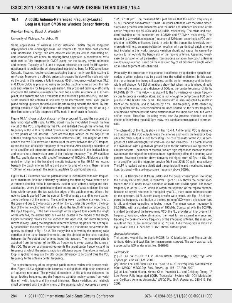
Figure 16.4.2 illustrates how the patch antenna is used to detect its own frequen-cy of maximum radiation efficiency by utilizing the standing-wave pattern on it.A transmission line model is commonly used in patch antenna design and char-acterization, where the open load end and source end of a transmission line withlarge width represent the two radiation edges of the patch antenna. When a fre-quency tone is applied from the source, it will generate a standing wave patternalong the length of the antenna. The standing wave magnitude is always fixed atthe open end due to the boundary condition there. Under this condition, the loca-tion of the first electric field null differs along the length dimension according tothe input frequency. If the half-wavelength of the applied tone equals the lengthof the antenna, the electric field null will be located in the middle of the length.Higher frequency moves the null closer to the open end, and lower frequencymoves it away. Taking the magnitude difference of two tap points that are equal-ly spaced from the center of the antenna results in a monotonic curve versus fre-quency as plotted in Fig. 16.4.2. The theory line is derived by the standing waveequation of the transmission line model, and the simulation line takes matchingbetween the PA output and antenna input into account. The measured data isacquired from the output of the EDs as frequency is swept across the range ofthe VCO. The zero-crossing point represents the target center frequency, and thefrequency at which the antenna radiation efficiency peaks. Therefore, a feedbackloop is applied to regulate the EDs output difference to zero and thus the VCOfrequency to the antenna center frequency.
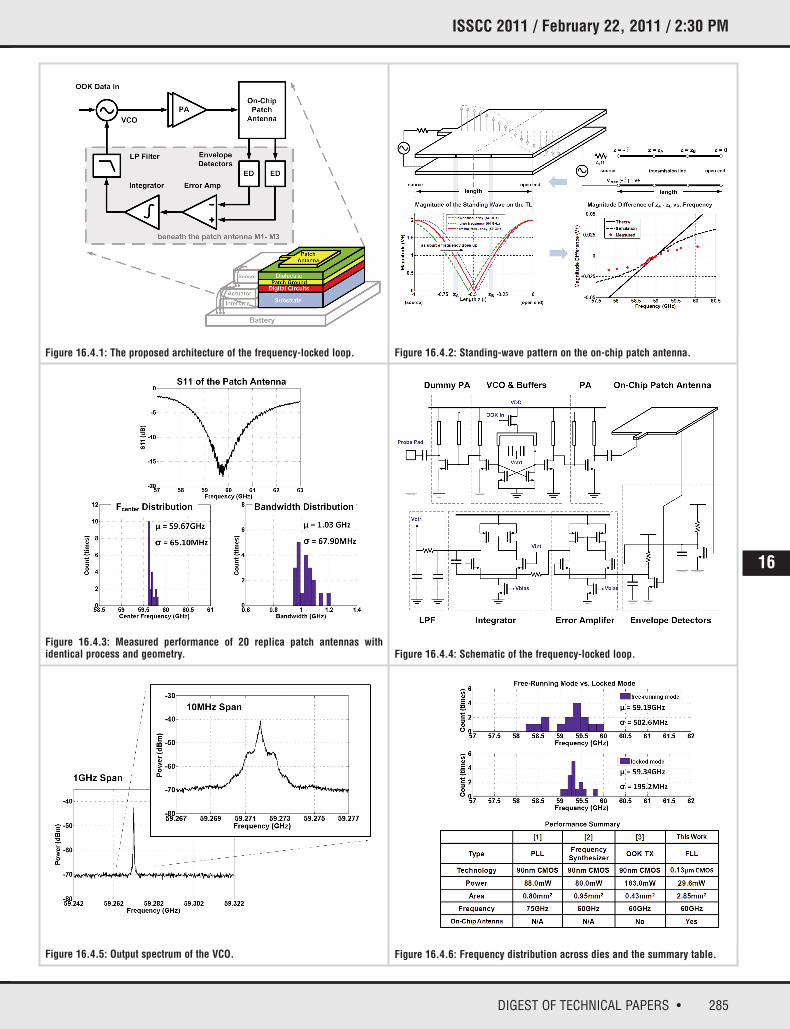
The center frequency of an integrated patch antenna varies with process varia-tion. Figure 16.4.3 highlights the accuracy of using an on-chip patch antenna asa frequency reference. The physical dimensions of the antenna determine thetarget locking frequency, and the frequency variation mainly comes from varia-tion on width, length and the metal thickness. These variations are relativelysmall compared with the dimensions of the antenna, which occupies an area of
1220 x 1580µm2. The measured S11 plot shows that the center frequency is59.8GHz and the bandwidth is 1.2GHz. 20 replica antennas with the same dimen-sions and process were measured, and the mean and standard deviation of thecenter frequency are 59.7GHz and 65.1MHz, respectively. The mean and stan-dard deviation of the bandwidth are 1.03GHz and 67.9MHz, respectively. Thisresults in a 3σ variation in center frequency of 3270ppm, ensuring it is FCC com-pliant in the 60GHz unlicensed band. In order for the transmitter to reliably com-municate with e.g. an energy-detection receiver with an identical patch antenna(not included in this work), process variation should not cause the center fre-quency to fall outside the bandwidth of the receive antenna. Assuming worst-case 3σ variation on all parameters from process variation, two patch antennaswould always overlap. Based on the measured S11 of 20 dies from a single wafer,no missed alignment was observed.
Practically, the properties of the antenna are affected by application-specific sce-narios in which objects may be placed near the radiating element. In this case,the transmission line theory still applies, but the center frequency and the band-width will change. Full EM simulations show that when metal is placed directlyin front of the antenna at a distance of 500µm, the center frequency shifts by67.6MHz (0.1%). This value is equivalent to the 1σ variance on center frequen-cy due to process variation alone, and is not enough to compromise FCC com-pliance in the 60GHz ISM band. The bandwidth is also impacted by metal infront of the antenna, and it reduces by 17%. The frequency shifts caused bynearby metal and by process variation are uncorrelated, so the center frequencyof a blocked antenna has the same distribution as the unblocked one, but with ashifted mean. Therefore, including worst-case 3σ process variation and theeffects of interfering metal 500µm away, two patch antennas can still communi-cate.
The schematic of the FLL is shown in Fig. 16.4.4. A differential VCO is designedso that one of the VCO outputs feeds the antenna and forms the feedback loop,while the other output is used for testing. The core resonator of the VCO is com-posed of a half-wavelength transmission line and varactors. The patch antennais drawn in M8 with a global M4 ground plane for the antenna allowing room forcircuits beneath. The inputs of the two EDs are high impedance loads so that thetwo taps on the edge of the antenna do not significantly affect the standing wavepattern. Envelope detection down-converts the signal from 60GHz to DC. Theerror amplifier and the integrator provide 20dB and 27dB DC gain, respectively.The LPF is realized using a distributed transmission line and metal comb capac-itors designed with a self-resonance frequency above 60GHz.
The FLL is fabricated in 0.13µm CMOS and the power consumption (excludingthe dummy PA to test pads) is 29.6mW. Figure 16.4.5 shows the output spec-trum of the VCO under locked condition at 1GHz and 10MHz spans. The lockedfrequency is at 59.27GHz, which is within the variation of the replica antenna.Because no crystal reference is multiplied by a PLL, there are no reference spurson the spectrum. 15 FLLs from a single wafer were tested, and Fig. 16.4.6 com-pares the frequency distribution of the free-running VCO when the feedback loopis off, and when operating in locked mode. The mean center frequency is59.34GHz, with a standard deviation of 195MHz. Compared with the 503MHzstandard deviation of the free-running VCO, the FLL provides an improvement infrequency variation, while eliminating the need for an external reference andtracking the peak-efficiency frequency of the integrated antenna. The measuredresults of the FLL are summarized in Fig. 16.4.6. A die micrograph is shown inFig. 16.4.7. The FLL occupies 1.60x1.78mm2 without pads.
Acknowledgements:The authors would like to thank MOSIS for IC fabrication, and Mona Jarrahi,Anthony Grbic, and Jack East for measurement support. The work was partiallysupported by NSF under grant No. 9986866.
References:[1] Jri Lee, “A 75-GHz PLL in 90-nm CMOS Technology,” ISSCC Dig. Tech.Papers, pp. 432-433, Feb. 2007.[2] Chihun Lee, and Shen-Iuan Liu, “A 58-to-60.4GHz Frequency Synthesizer in90nm CMOS,” ISSCC Dig. Tech. Papers, pp. 195-197, Feb. 2007. [3] Jri Lee, Yenlin Huang, Yentso Chen, Hsinchia Lu, and Chiajung Chang, “ALow-Power Fully Integrated 60GHz Transceiver System with OOK Modulationand On-Board Antenna Assembly,” ISSCC Dig. Tech. Papers, pp. 315-316, Feb.2009.
978-1-61284-302-5/11/$26.00 ©2011 IEEE
285DIGEST OF TECHNICAL PAPERS •
ISSCC 2011 / February 22, 2011 / 2:30 PM
Figure 16.4.1: The proposed architecture of the frequency-locked loop. Figure 16.4.2: Standing-wave pattern on the on-chip patch antenna.
Figure 16.4.3: Measured performance of 20 replica patch antennas with identical process and geometry.
Figure 16.4.5: Output spectrum of the VCO. Figure 16.4.6: Frequency distribution across dies and the summary table.
Figure 16.4.4: Schematic of the frequency-locked loop.
16
• 2011 IEEE International Solid-State Circuits Conference 978-1-61284-302-5/11/$26.00 ©2011 IEEE
ISSCC 2011 PAPER CONTINUATIONS
Figure 16.4.7: Die Micrograph.