ISOFACE™ ISO1H812G protection † Very low standby current † Reverse battery protection †...
23
Power Management & Multimarket Datasheet Revision 2.5, 2013-05-16 ISO1H812G Galvanic Isolated 8 Channel High-Side Switch ISOFACE™
Transcript of ISOFACE™ ISO1H812G protection † Very low standby current † Reverse battery protection †...

Power Management & Mult imarket
Datasheet Revision 2.5, 2013-05-16
ISO1H812GGalvanic Isolated 8 Channel High-Side Switch
ISOFACE™
Edition 2013-05-16Published byInfineon Technologies AG81726 Munich, Germany© 2013 Infineon Technologies AGAll Rights Reserved.
Legal DisclaimerThe information given in this document shall in no event be regarded as a guarantee of conditions or characteristics. With respect to any examples or hints given herein, any typical values stated herein and/or any information regarding the application of the device, Infineon Technologies hereby disclaims any and all warranties and liabilities of any kind, including without limitation, warranties of non-infringement of intellectual property rights of any third party.
InformationFor further information on technology, delivery terms and conditions and prices, please contact the nearest Infineon Technologies Office (www.infineon.com).
WarningsDue to technical requirements, components may contain dangerous substances. For information on the types in question, please contact the nearest Infineon Technologies Office.Infineon Technologies components may be used in life-support devices or systems only with the express written approval of Infineon Technologies, if a failure of such components can reasonably be expected to cause the failure of that life-support device or system or to affect the safety or effectiveness of that device or system. Life support devices or systems are intended to be implanted in the human body or to support and/or maintain and sustain and/or protect human life. If they fail, it is reasonable to assume that the health of the user or other persons may be endangered.
ISOFACE™ISO1H812G
Datasheet 3 Revision 2.5, 2013-05-16
Trademarks of Infineon Technologies AGAURIX™, C166™, CanPAK™, CIPOS™, CIPURSE™, EconoPACK™, CoolMOS™, CoolSET™,CORECONTROL™, CROSSAVE™, DAVE™, DI-POL™, EasyPIM™, EconoBRIDGE™, EconoDUAL™,EconoPIM™, EconoPACK™, EiceDRIVER™, eupec™, FCOS™, HITFET™, HybridPACK™, I²RF™,ISOFACE™, IsoPACK™, MIPAQ™, ModSTACK™, my-d™, NovalithIC™, OptiMOS™, ORIGA™,POWERCODE™; PRIMARION™, PrimePACK™, PrimeSTACK™, PRO-SIL™, PROFET™, RASIC™,ReverSave™, SatRIC™, SIEGET™, SINDRION™, SIPMOS™, SmartLEWIS™, SOLID FLASH™, TEMPFET™,thinQ!™, TRENCHSTOP™, TriCore™.
Other TrademarksAdvance Design System™ (ADS) of Agilent Technologies, AMBA™, ARM™, MULTI-ICE™, KEIL™,PRIMECELL™, REALVIEW™, THUMB™, µVision™ of ARM Limited, UK. AUTOSAR™ is licensed by AUTOSARdevelopment partnership. Bluetooth™ of Bluetooth SIG Inc. CAT-iq™ of DECT Forum. COLOSSUS™,FirstGPS™ of Trimble Navigation Ltd. EMV™ of EMVCo, LLC (Visa Holdings Inc.). EPCOS™ of Epcos AG.FLEXGO™ of Microsoft Corporation. FlexRay™ is licensed by FlexRay Consortium. HYPERTERMINAL™ ofHilgraeve Incorporated. IEC™ of Commission Electrotechnique Internationale. IrDA™ of Infrared DataAssociation Corporation. ISO™ of INTERNATIONAL ORGANIZATION FOR STANDARDIZATION. MATLAB™ ofMathWorks, Inc. MAXIM™ of Maxim Integrated Products, Inc. MICROTEC™, NUCLEUS™ of Mentor GraphicsCorporation. MIPI™ of MIPI Alliance, Inc. MIPS™ of MIPS Technologies, Inc., USA. muRata™ of MURATAMANUFACTURING CO., MICROWAVE OFFICE™ (MWO) of Applied Wave Research Inc., OmniVision™ ofOmniVision Technologies, Inc. Openwave™ Openwave Systems Inc. RED HAT™ Red Hat, Inc. RFMD™ RFMicro Devices, Inc. SIRIUS™ of Sirius Satellite Radio Inc. SOLARIS™ of Sun Microsystems, Inc. SPANSION™of Spansion LLC Ltd. Symbian™ of Symbian Software Limited. TAIYO YUDEN™ of Taiyo Yuden Co.TEAKLITE™ of CEVA, Inc. TEKTRONIX™ of Tektronix Inc. TOKO™ of TOKO KABUSHIKI KAISHA TA. UNIX™of X/Open Company Limited. VERILOG™, PALLADIUM™ of Cadence Design Systems, Inc. VLYNQ™ of TexasInstruments Incorporated. VXWORKS™, WIND RIVER™ of WIND RIVER SYSTEMS, INC. ZETEX™ of DiodesZetex Limited.Last Trademarks Update 2011-11-11
Revision HistoryPage or Item Subjects (major changes since previous revision)Revision 2.5, 2013-05-16Page 13 Page 13, Table 4.1 Extended operating temperature footnote removedRevision 2.4Page 13 Page 13, Table 4.1 Extended operating temperature addedRevision 2.3Page 14 Page 14, Table 4.3 updated
Page 18 Page 18 Table 4.8 updated
Revision 2.2Page 5 Page 5, Figure 1 updatedRevision 2.1all Data for parallel channels and UL approval addedRevision 2.0all Final Datasheet
Type On-state Resistance Package
ISO1H812G 200mΩ PG-DSO36
Datasheet 4 Revision 2.5, 2013-05-16
ISOFACE™ISO1H812G
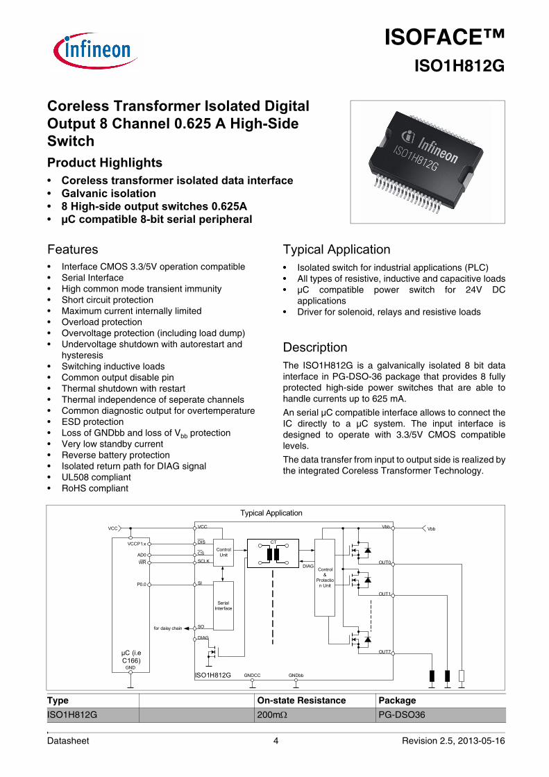
Coreless Transformer Isolated Digital Output 8 Channel 0.625 A High-Side SwitchProduct Highlights• Coreless transformer isolated data interface• Galvanic isolation• 8 High-side output switches 0.625A• µC compatible 8-bit serial peripheral
ISO1H812G
µC (i.e C166)
AD0WR
P0.0
P1.xVCC
VCC
Serial Interface
Control Unit
CT
Control &
Protection Unit
CS
SCLK
SI
DIS
VCC
GNDCC GNDbb
GND
OUT7
VbbVbb
OUT1
OUT0
Typical Application
DIAG
DIAG
SOfor daisy chain
Features• Interface CMOS 3.3/5V operation compatible• Serial Interface• High common mode transient immunity• Short circuit protection• Maximum current internally limited• Overload protection• Overvoltage protection (including load dump)• Undervoltage shutdown with autorestart and
hysteresis• Switching inductive loads• Common output disable pin• Thermal shutdown with restart• Thermal independence of seperate channels• Common diagnostic output for overtemperature• ESD protection• Loss of GNDbb and loss of Vbb protection• Very low standby current• Reverse battery protection• Isolated return path for DIAG signal• UL508 compliant• RoHS compliant
Typical Application• Isolated switch for industrial applications (PLC)• All types of resistive, inductive and capacitive loads• µC compatible power switch for 24V DC
applications• Driver for solenoid, relays and resistive loads
DescriptionThe ISO1H812G is a galvanically isolated 8 bit datainterface in PG-DSO-36 package that provides 8 fullyprotected high-side power switches that are able tohandle currents up to 625 mA.
An serial µC compatible interface allows to connect theIC directly to a µC system. The input interface isdesigned to operate with 3.3/5V CMOS compatiblelevels.
The data transfer from input to output side is realized bythe integrated Coreless Transformer Technology.

ISOFACE™ISO1H812G
Pin Configuration and Functionality
Datasheet 5 Revision 2.5, 2013-05-16
1 Pin Configuration and Functionality
1.1 Pin Configuration
Figure 1 Power SO-36 (430mil)
.
Pin Symbol Function1 N.C. Not connected2 VCC Positive 3.3/5V logic supply3 DIS Output disable4 CS Chip select5 SCLK Serial Clock6 SI Serial Data input7 N.C. Not connected8 N.C. Not connected9 N.C. Not connected
10 N.C. Not connected11 N.C. Not connected12 N.C. Not connected13 SO Serial Data Output14 DIAG Common diagnostic output for
overtemperature15 GNDCC Input logic ground16 N.C. Not connected17 N.C. Not connected18 N.C. Not connected19 GNDbb Output driver ground20 N.C Not connected21 OUT7 High-side output of channel 722 OUT7 High-side output of channel 723 OUT6 High-side output of channel 624 OUT6 High-side output of channel 625 OUT5 High-side output of channel 526 OUT5 High-side output of channel 527 OUT4 High-side output of channel 428 OUT4 High-side output of channel 429 OUT3 High-side output of channel 330 OUT3 High-side output of channel 331 OUT2 High-side output of channel 232 OUT2 High-side output of channel 233 OUT1 High-side output of channel 134 OUT1 High-side output of channel 135 OUT0 High-side output of channel 036 OUT0 High-side output of channel 0
TAB Vbb Positive driver power supply voltage
VCC
N.C.
1
DISCS
SCLK 54
23
N.C.
N.C.
N.C.
N.C.
SI 678910
N.C.11
SO12
DIAG13
GNDCC1415
N.C. 161718
36
3233
3534
31302928272625242322212019
OUT0
OUT2
OUT0OUT1OUT1
OUT3
OUT4
OUT3
OUT4
OUT2
OUT5OUT5OUT6OUT6
GNDbb
OUT7OUT7N.C.
N.C.N.C.
N.C.Vbb
Vbb
TAB
TAB

Datasheet 6 Revision 2.5, 2013-05-16
ISOFACE™ISO1H812G
Pin Configuration and Functionality
1.2 Pin FunctionalityVCC (Positive 3.3/5V logic supply)The VCC supplies the input interface that isgalvanically isolated from the output driver stage. Theinput interface can be supplied with 5V.
DIS (Output disable)The high-side outputs OUT0...OUT7 can beimmediately switched off by means of the low active pinDIS that is an asynchronous signal. The input registersare also reset by the DIS signal. The output remainsswitched off after low-high transient of DIS, till new datais written into the input interface. Current Sink toGNDCC
CS (Chip select)The system microcontroller selects the ISO1H812G bymeans of the low active pin CS to activate the interface.Current Source to VCC
SCLK (Serial shift clock)SCLK (serial clock) is used to synchronize the datatransfer between the master and the ISO1H802G. Datapresent at the SI pin are latched on the rising edge ofthe serial clock input, while data at the SO pin isupdated after the falling edge of SCLK in serial mode.Current Source to VCC
SI (Serial data input)This pin is used to transfer data into the device. Data islatched on the rising edge of the serial clock. CurrentSink to GNDCC
SO (Serial data output) This pin is used when the serial interface is activated.SO can be connected to a serial input of a further IC tobuilt a daisy-chain configuration. It is only actvated if CSis in low state, otherwise this output is in highimpedance state.
DIAG (Common diagnostic output for overtemperature)The low active DIAG signal contains the OR-wiredinformation of the separated overtemperature detectionunits for each channel.The output pin DIAG provides anopen drain functionality that. A current source is alsoconnected to the pin DIAG. In normal operation thesignal DIAG is high. When overtemperature or Vbbbelow ON-Limit is detected the signal DIAG changes tolow.
GNDCC (Ground for VCC domain)This pin acts as the ground reference for the inputinterface that is supplied by VCC.
GNDbb (Output driver ground domain)This pin acts as the ground reference for the outputdriver that is supplied by Vbb.
OUT0 ... OUT7 (High side output channel 0 ... 7)The output high side channels are internally connectedto Vbb and controlled by the corresponding data input.
TAB (Vbb, Positive supply for output driver)The heatslug is connected to the positive supply port ofthe output interface.

Datasheet 7 Revision 2.5, 2013-05-16
ISOFACE™ISO1H812G
Blockdiagram
2 Blockdiagram
Figure 2 Blockdiagram
Seria
l In
put I
nter
face
SO
SCLKCS
Ove
rvol
tage
Pr
otec
tion
Und
ervo
ltage
Sh
utdo
wn
with
R
esta
rt
Volta
ge
Sour
ce
Com
mon
D
iagn
ostic
Out
put
CT
Seria
l to
Pa
ralle
l
to L
ogic
Cha
nnel
1 -
6
Tem
pera
ture
Sen
sor
OU
T0
Ove
rload
Pro
tect
ion
Cur
rent
Lim
itatio
n
Lim
itatio
n of
Unc
lam
ped
Indu
ctive
Loa
dLo
gic
Cha
rge
Pum
pLe
vel s
hifte
rR
ectif
ier
Hig
h-sid
e C
hann
el
0
Tem
pera
ture
Sen
sor
OU
T7
Ove
rload
Pro
tect
ion
Cur
rent
Lim
itatio
n
Lim
itatio
n of
Unc
lam
ped
Indu
ctive
Loa
dLo
gic
Cha
rge
Pum
pLe
vel S
hifte
rR
ectif
ier
Hig
h-sid
e C
hann
el
7
Cha
nnel
1 ..
. 6
from
Te
mpe
ratu
re
Sens
orC
hann
el 1
-6
to L
ogic
Cha
nnel
1 -
6
Vbb
Logi
cU
nder
volta
ge
Shut
dow
n w
ith
Res
tart
Vbb
GN
Dbb
VCC
GN
DC
C
Galvanic Isolation
DIS
OU
T1
OU
T2
OU
T3
OU
T4
OU
T5
OU
T6
Gat
e Pr
otec
tion
Gat
e Pr
otec
tion
ISO
1H81
2G
100µ
A
DIA
G
VCC
SI

ISOFACE™ISO1H812G
Functional Description
Datasheet 8 Revision 2.5, 2013-05-16
3 Functional Description
3.1 IntroductionThe ISOface ISO1H812G includes 8 high-side powerswitches that are controlled by means of the integratedµC compatible SPI interface. The outputsOUT0...OUT7 are controlled by the data of the serialinput SI. The IC can replace 8 optocouplers and the 8high-side switches in conventional I/O-Applications asa galvanic isolation is implemented by means of theintegrated coreless transformer technology. The µCcompatible interfaces allow a direct connection to theports of a microcontroller without the need for othercomponents. Each of the 8 high-side power switches isprotected against short to Vbb, overload,overtemperature and against overvoltage by an activezener clamp.The diagnostic logic on the power chip recognizes theovertemperature information of each power transistorThe information is send via the internal corelesstransformer to the pin DIAG at the input interface.
3.2 Power SupplyThe IC contains 2 galvanic isolated voltage domainsthat are independent from each other. The inputinterface is supplied at VCC and the output stage issupplied at Vbb. The different voltage domains can beswitched on at different time. The output stage is onlyenabled once the input stage enters a stable state.
3.3 Output StageEach channel contains a high-side vertical power FETthat is protected by embedded protection functions.The continuous current for each channel is 625mA (allchannels ON).
3.3.1 Output Stage ControlEach output is independently controlled by an outputlatch and a common reset line via the pin DIS thatdisables all eight outputs and reset the latches. Serialdata input (SI) is read on the rising edge of the serialclock SCLK. A logic high input data bit turns therespective output channel ON, a logic low data bit turnsit OFF. CS must be low whilst shifting all the serial datainto the device. A low-to-high transition of CS transfersthe serial data input bits to the output buffer.
3.3.2 Power Transistor Overvoltage Protection
Each of the eight output stages has its own zener clampthat causes a voltage limitation at the power transistorwhen solenoid loads are switched off. VON is thenclamped to 47V (min.).
Figure 3 Inductive and overvoltage output clamp (each channel)
Energy is stored in the load inductance during aninductive load switch-off.
Figure 4 Inductive load switch-off energy dissipation (each channel)
While demagnetizing the load inductance, the energydissipation in the DMOS is
with an approximate solution for RL > 0Ω:
Vz
Vbb
GNDbbOUTx
VON
Vbb
EL 1 2⁄ L IL2××=
ELGNDbbVbb
OUTx
ER
L
RL
ELoad
ZL
Vbb
EbbEAS
Dx
EAS Ebb EL ER– VON CL( ) iL t( )dt×=+=
EASIL L×2 RL×---------------- Vbb VON CL( )+( ) 1
IL RL×VON CL( )-------------------------+⎝ ⎠
⎛ ⎞ln××=

Datasheet 9 Revision 2.5, 2013-05-16
ISOFACE™ISO1H812G
Functional Description
3.3.3 Power Transistor Overcurrent Protection
The outputs are provided with a current limitation thatenters a repetitive switched mode after an initial peakcurrent has been exceeded. The initial peak shortcircuit current limit is set to IL(SCp) at Tj = 125°C. Duringthe repetitive mode short circuit current limit is set toIL(SCr). If this operation leads to an overtemperaturecondition, a second protection level (Tj > 135°C) willchange the output into a low duty cycle PWM (selectivethermal shutdown with restart) to prevent critical chiptemperatures.
Figure 5 Overtemperature detection
The following figures show the timing for a turn on intoshort circuit and a short circuit in on-state. Heating upof the chip may require several milliseconds,depending on external conditions.
Figure 6 Turn on into short circuit, shut down by overtemperature, restart by cooling
Figure 7 Short circuit in on-state, shut downdown by overtemperature, restart bycooling
3.4 Common Diagnostic OutputThe overtemperature detection information are OR-wired in the common diagnostic output block. Theinformation is send via the integrated corelesstransformer to the input interface. The output stage atpin DIAG has an open drain functionality combined witha current source.
Figure 8 Common diagnostic output
IN
VOUT
TJ
t
t
t
t
DIAG
IN
VOUT
IL
t
t
t
t
DIAG
Output short to GND
IL(SCp) IL(SCr)
IN
VOUT
IL
t
t
t
t
DIAG
Output short to GND
IL(SCp) IL(SCr)
Normaloperation
CommonDiagnostic
OutputCT100µA
VCC
DIAG
Datasheet 10 Revision 2.5, 2013-05-16
ISOFACE™ISO1H812G
Functional Description
3.5 Serial InterfaceThe ISO1H812G contains a serial interface that can bedirectly controlled by the microcontroller output ports.
3.5.1 SPI Signal DescriptionCS - Chip select. The system microcontroller selectsthe ISO1H812G by means of the CS pin. Whenever thepin is in a logic low state, data can be transferred fromthe µC. CS High to low transition:
•Serial input data can be clocked in from then on •SO changes from high impendance state to logic highor low state corresponding to the SO bit-state CS Low to high transition:
•Transfer of SI bits from shift register into outputbuffers, if number of clock signals was an integermultiple of 8 •SO changes from the SO bit-state to high impendancestate
To avoid any false clocking the serial input pin SCLKshould be logic high state during high-to-low transitionof CS. When CS is in a logic high state, any signals atthe SCLK and SI pins are ignored and SO is forced intoa high impedance state. The integrated modulo counterthat counts the number of clocks avoids the take overof invalid commands caused by a spike on the clockline or wrong number of clock cycles. A command isonly taken over if after the low-to-high transition of theCS signal the number of counted clock cycles is aninteger multiple of 8. SCLK - Serial clock. The system clock pin clocks theinternal shift register of the ISO1H812G. The serialinput (SI) accepts data into the input shift register on therising edge of SCLK while the serial output (SO) shiftsthe output information out of the shift register on thefalling edge of the serial clock. It is essential that theSCLK pin is in a logic high state whenever chip selectCS makes any transition. The number of clock pulseswill be counted during a chip select cycle. The receiveddata will only be accepted, if exactly an integer multipleof 8 clock pulses were counted during CS is active.
SI - Serial input. Serial data bits are shifted in at this pin,the most significant bit first. SI information is read in onthe rising edge of the SCLK. Input data is latched in theshift register and then transferred to the control bufferof the output stages. SO - Serial output. SO is in a high impedance state untilthe CS pin goes to a logic low state. The data of theinternal shift register are shifted out serially at this pin.The most significant bit will appear at first. The furtherbits will appear following the falling edge of SCLK.
3.5.2 SPI Bus Concepts
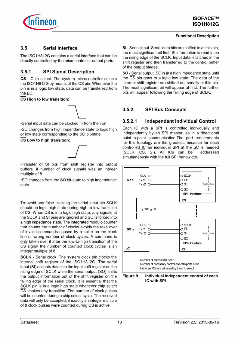
3.5.2.1 Independent Individual ControlEach IC with a SPI is controlled individually andindependently by an SPI master, as in a directionalpoint-to-point communication.The port requirementsfor this topology are the greatest, because for eachcontrolled IC an individual SPI at the µC is needed(SCLK, CS, SI). All ICs can be addressedsimultaneously with the full SPI bandwidth.
Figure 9 Individual independent control of each IC with SPI
SPI - Interface
IC1
Output lines
SPI - Interface
ICn
Output lines
µC
SPI 1
SPI n
SCLKCSSI
SCLKCSSI
CLKTx a1Tx a2
CLKTx n1Tx n2
Number of adressed ICs = nNumber of necessary control and data ports = 3 nIndividual ICs are adressed by the chip select
SO
SO
Datasheet 11 Revision 2.5, 2013-05-16
ISOFACE™ISO1H812G
Functional Description
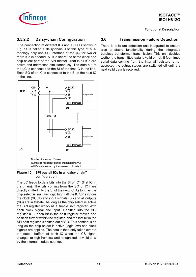
3.5.2.2 Daisy-chain Configuration The connection of different ICs and a µC as shown inFig. 11 is called a daisy-chain. For this type of bus-topology only one SPI interface of the µC for two ormore ICs is needed. All ICs share the same clock andchip select port of the SPI master. That is all ICs areactive and addressed simultaneously. The data out ofthe µC is connected to the SI of the first IC in the line.Each SO of an IC is connected to the SI of the next ICin the line.
Figure 10 SPI bus all ICs in a “daisy chain” configuration
The µC feeds to data bits into the SI of IC1 (first IC inthe chain). The bits coming from the SO of IC1 aredirectly shifted into the SI of the next IC. As long as thechip select is inactive (logic high) all the IC SPIs ignorethe clock (SCLK) and input signals (SI) and all outputs(SO) are in tristate. As long as the chip select is activethe SPI register works as a simple shift register. Witheach clock signal one input is shifted into the SPIregister (SI), each bit in the shift register moves oneposition further within the register, and the last bit in theSPI shift register is shifted out of SO. This continous aslong as the chip select is active (logic low) and clocksignals are applied. The data is then only taken over tothe output buffers of each IC when the CS signalchanges to high from low and recognized as valid databy the internal modulo counter.
3.6 Transmission Failure DetectionThere is a failure detection unit integrated to ensurealso a stable functionality during the integratedcoreless transformer transmission. This unit decideswether the transmitted data is valid or not. If four timesserial data coming from the internal registers is notaccepted the output stages are switched off until thenext valid data is received.
SPI - Interface
Output lines
SPI - Interface
Output lines
µC
SPI 1CLK
Tx a1Tx a2
Number of adressed ICs = nNumber of necessary control and data ports = 3All ICs are adressed by the common chip select
ICn
IC1
SCLKCSSI
SCLKCS
SO
SI
ISOFACE™ISO1H812G
Functional Description
Datasheet 12 Revision 2.5, 2013-05-16
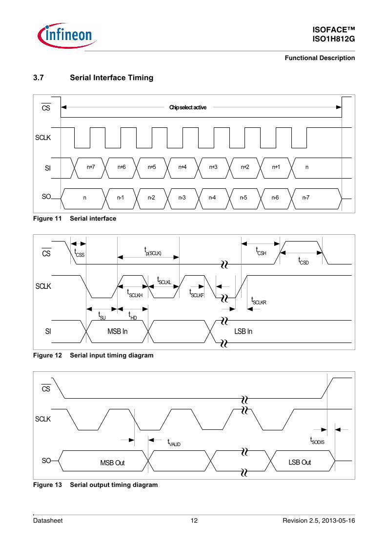
3.7 Serial Interface Timing
Figure 11 Serial interface
Figure 12 Serial input timing diagram
Figure 13 Serial output timing diagram
CS
SCLK
SI n+7 n+6 n+5 n+4 n+3 n+2 n+1 n
n-1 n-2 n-3 n-4 n-5 n-6 n-7SO n
Chip select active
CS
SCLK
SI
tCSStCSH
tSCLKH
tSCLKL
tCSD
tSU tHD
≈≈
≈≈
tp(SCLK)
tSCLKF tSCLKR
MSB In LSB In
CS
SCLK
SO
≈≈
tVALID
MSB Out LSB Out
≈≈
tSODIS

Datasheet 13 Revision 2.5, 2013-05-16
ISOFACE™ISO1H812G
Electrical Characteristics
4 Electrical CharacteristicsNote: All voltages at pins 2to 14 are measured with respect to ground GNDCC (pin 15). All voltages at pin 20 to
pin 36 and TAB are measured with respect to ground GNDbb (pin 19). The voltage levels are valid if otherratings are not violated. The two voltage domains VCC ,GNDCC and Vbb ,GNDbb are internally galvanicisolated.
4.1 Absolute Maximum RatingsNote: Absolute maximum ratings are defined as ratings, which when being exceeded may lead to destruction of
the integrated circuit. For the same reason make sure, that any capacitor that will be connected to pin 2(VCC) and TAB (Vbb) is discharged before assembling the application circuit. Supply voltages higher thanVbb(AZ) require an external current limit for the GNDbb pin, e.g. with a 15Ω resistor in GNDbb connection.Operating at absolute maximum ratings can lead to a reduced lifetime.
Parameterat Tj = -40 ... 135°C, unless otherwise specified
Symbol Limit Values Unitmin. max.
Supply voltage input interface (VCC) VCC -0.5 6.5 V
Supply voltage output interface (Vbb) Vbb -11)
1) defined by Ptot
45Continuos voltage at pin SI VDx -0.5 6.5Continuos voltage at pin CS VCS -0.5 6.5Continuos voltage at pin SCLK VWR -0.5 6.5Continuos voltage at pin DIS VDIS -0.5 6.5Continuos voltage at pin SO VDx -0.5 6.5Continuos voltage at pin DIAG VDIAG -0.5 6.5Load current (short-circuit current) IL --- self limited A
Reverse current through GNDbb1) IGNDbb -1.6 ---Operating Temperature Tj -25 internal limited °C
Extended Operation Temperature Tj -40 internal limited
Storage Temperature Tstg -50 150Power Dissipation2)
2) Device on 50mm*50mm*1.5mm epoxy PCB FR4 with 6cm² (one layer, 70µm thick) copper area for drain connection. PCBis vertical without blown air.
Ptot --- 3.3 W
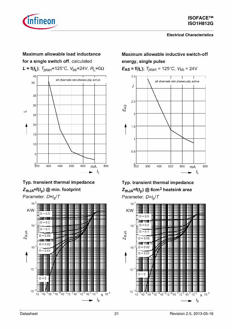
Inductive load switch-off energy dissipation3) single pulse, Tj = 125°C, IL = 0.625Aone channel activeall channel simultaneously active (each channel)
3) not subject to production test, specified by design
EAS
--- 101
J
Load dump protection3) VloadDump4)=VA + VS
VIN = low or hightd = 400ms, RI = 2W, RL = 27W, VA = 13.5Vtd = 350ms, RI = 2W, RL = 57W, VA = 27V
VLoaddump
------
90117
V
Electrostatic discharge voltage (Human Body Model)according to JESD22-A114-B
VESD2
kV
Electrostatic discharge voltage (Charge Device Model)according to ESD STM5.3.1 - 1999
VESD1
kV
Continuos reverse drain current1)3), each channel IS --- 4 A

ISOFACE™ISO1H812G
Electrical Characteristics
Datasheet 14 Revision 2.5, 2013-05-16
4.2 Thermal Characteristics
4.3 Load Switching Capabilities and Characteristics
4) VLoaddump is setup without the DUT connected to the generator per ISO7637-1 and DIN40839
Parameterat Tj = -25 ... 125°C, Vbb=15...30V, VCC= 3.0...5.5V, unless otherwise specified
Symbol Limit Values Unit Test Conditionmin. typ. max.
Thermal resistance junction - case RthJC --- --- 1.5 K/W
Thermal resistance @ min. footprint Rth(JA) --- --- 50
Thermal resistance @ 6cm² cooling area1)
1) Device on 50mm*50mm*1.5mm epoxy PCB FR4 with 6cm² (one layer, 70µm thick) copper area for drain connection. PCBis vertical without blown air.
Rth(JA) --- --- 38
Parameterat Tj = -25 ... 125°C, Vbb=15...30V, VCC= 3.0...5.5V, unless otherwise specified
Symbol Limit Values Unit Test Conditionmin. typ. max.
On-state resistance, IL = 0.5A, each channelTj = 25°CTj = 125°C
two parallel channels, Tj = 25°C:1)
four parallel channels, Tj = 25°C:1)
RON
------
1502707538
20032010050
mΩ
Nominal load currentDevice on PCB 38K/W, Ta = 85°C, Tj < 125°C
one channel:1)
two parallel channels:1)
four parallel channels:1)
1) not subject to production test, specified by design
IL(NOM) 0.71.12.2
A
Turn-on time to 90% VOUT2)
RL = 47Ω, VDx = 0 to 5V
2) The turn-on and turn-off time includes the switching time of the high-side switch and the transmission time via the corelesstransformer in normal operating mode. During a failure on the coreless transformer transmission turn-on or turn-off timecan increase by up to 50µs.
ton --- 64 120 µs
Turn-off time to 10% VOUT1)
RL = 47Ω, VDx = 5 to 0Vtoff --- 89 170
Slew rate on 10 to 30% VOUTRL = 47Ω, Vbb = 15V
dV/dton --- 1 2 V/µs
Slew rate off 70 to 40% VOUTRL = 47Ω, Vbb = 15V
-dV/dtoff --- 1 2
Internal data transmission period tidt 17,8 µs 1)
Failure shutdown time tfs 64 µs 1)
Datasheet 15 Revision 2.5, 2013-05-16
ISOFACE™ISO1H812G
Electrical Characteristics
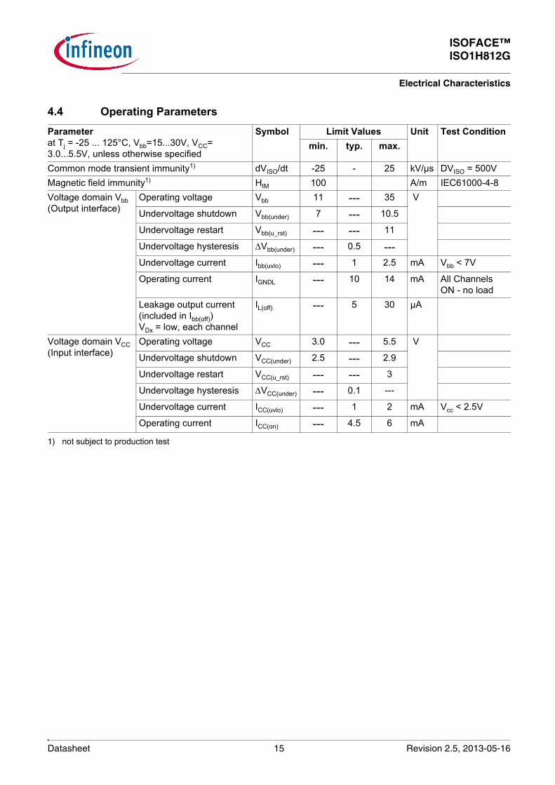
4.4 Operating ParametersParameterat Tj = -25 ... 125°C, Vbb=15...30V, VCC= 3.0...5.5V, unless otherwise specified
Symbol Limit Values Unit Test Conditionmin. typ. max.
Common mode transient immunity1)
1) not subject to production test
dVISO/dt -25 - 25 kV/µs DVISO = 500VMagnetic field immunity1) HIM 100 A/m IEC61000-4-8Voltage domain Vbb (Output interface)
Operating voltage Vbb 11 --- 35 V
Undervoltage shutdown Vbb(under) 7 --- 10.5
Undervoltage restart Vbb(u_rst) --- --- 11
Undervoltage hysteresis ΔVbb(under) --- 0.5 ---Undervoltage current Ibb(uvlo) --- 1 2.5 mA Vbb < 7V
Operating current IGNDL --- 10 14 mA All Channels ON - no load
Leakage output current (included in Ibb(off))VDx = low, each channel
IL(off) --- 5 30 µA
Voltage domain VCC (Input interface)
Operating voltage VCC 3.0 --- 5.5 V
Undervoltage shutdown VCC(under) 2.5 --- 2.9
Undervoltage restart VCC(u_rst) --- --- 3
Undervoltage hysteresis ΔVCC(under) --- 0.1 ---
Undervoltage current ICC(uvlo) --- 1 2 mA Vcc < 2.5V
Operating current ICC(on) --- 4.5 6 mA

ISOFACE™ISO1H812G
Electrical Characteristics
Datasheet 16 Revision 2.5, 2013-05-16
4.5 Output Protection Functions
4.6 Diagnostic Characteristics at pin DIAG
Parameter1)
at Tj = -25 ... 125°C, Vbb=15...30V, VCC=3.0...5.5V, unless otherwise specified
1) Integrated protection functions are designed to prevent IC destruction under fault conditions described in the data sheet.Fault conditions are considered as “outside” normal operating range. Protection functions are not designed for continuosrepetitive operation.
Symbol Limit Values Unit Test Conditionmin. typ. max.
Initial peak short circuit current limit, each channel:Tj = -25°C, Vbb = 30V, tm = 700µsTj = 25°CTj = 125°C
two parallel channels:3)
four parallel channels:3)
IL(SCp)------0.7
---1.4---
1.9------
A
twice the current of one channelfour times the current of one channel
Repetitive short circuit current limitTj = Tjt (see timing diagrams)
each channel:two parallel channels:3)
four parallel channels:3)
IL(SCr)
---
1.11.11.1
---
Repetitive short circuit current limit3)
Tj = Tjt (see timing diagrams)IL(SCr) --- 1.1 ---
Output clamp (inductive load switch off)at VOUT = Vbb - VON(CL)
VON(CL) 47 53 60 V
Overvoltage protection Vbb(AZ) 47 --- ---Thermal overload trip temperature2) 3)
2) Higher operating temperature at normal function for each channel available3) not subject to production test, specified by design
Tjt 135 --- --- °C
Thermal hysteresis3) ΔTjt --- 10 --- K
Parameterat Tj = -25 ... 125°C, Vbb=15...30V, VCC=3.0...5.5V, unless otherwise specified
Symbol Limit Values Unit Test Conditionmin. typ. max.
Common diagnostic sink current (overtemperature of any channel) Tj = 135°C
Idiagsink 5 mA VDIAGON < 0.25 x VCC
Common diagnostic source current Idiagsource 100 µA

Datasheet 17 Revision 2.5, 2013-05-16
ISOFACE™ISO1H812G
Electrical Characteristics
4.7 Input Interface
Parameterat Tj = -25 ... 125°C, Vbb=15...30V, VCC= 3.0...5.5V, unless otherwise specified
Symbol Limit Values Unit Test Conditionmin. typ. max.
Input low state voltage (SI, DIS, CS, SCLK)
VIL -0.3 --- 0.3 x VCC
V
Input high state voltage (SI, DIS, CS, SCLK)
VIH 0.7 x VCC
--- VCC+ 0.3
Input voltage hysteresis (SI, DIS, CS, SCLK)
VIHys 100 mV
Output low state voltage (SO)
VOL -0.3 --- 0.25 x VCC
V CL < 50pF,RL > 10kΩ
Output high state voltage (SO)
VOH 0.75 x VCC
--- VCC+ 0.3
Input pull down current(SI , DIS)
IIdown 100 µA
Input pull up current(CS, SCLK)
-IIup 100
Output disable time (transition DIS to logic low)1)2)
Normal operationTurn-off time to 10% VOUTRL = 47Ω
1) The time includes the turn-on/off time of the high-side switch and the transmission time via the coreless transformer.2) If Pin DIS is set to low the outputs are set to low; after DIS set to high a new write cycle is necessary to set the output again.
tDIS --- 85 170 µs
Output disable time (transition DIS to logic low)1)2)3)
Disturbed operationTurn-off time to 10% VOUTRL = 47Ω
3) The parameter is not subject to production test - verified by design/characterization
tDIS --- --- 230

ISOFACE™ISO1H812G
Electrical Characteristics
Datasheet 18 Revision 2.5, 2013-05-16
4.8 SPI Timing
4.9 Reverse Voltage
Parameterat Tj = -25 ... 125°C, Vbb=15...30V, VCC= 3.0...5.5V, unless otherwise specified
Symbol Limit Values Unit Test Conditionmin. typ. max.
Serial clock frequency fSCLK DC --- 20 MHz
Serial clock period (1/fclk) tp(SLCK) 50 --- --- ns
CS Setup time (falling edge of CS to falling edge of SCLK)
tCSS 5 --- ---
CS Hold time (rising edge of SCLK to rising edge of CS)
tCSH 10 --- ---
Data setup time (required time SI to rising edge of SCLK)
tSU 6 --- ---
Data hold time (falling edge of SCLK to SI) tHD 6 --- ---SO Output valid timeCL = 50pF
tVALID--- --- 20
SO Output disable time tSODIS 20 ns
Delay to next CS cycle tCSD 17,8 µs 1)
1) not subject to production test, specified by design
Input to output data transmission jitter tIOJ 8 17,8 1)
Parameterat Tj = -25 ... 125°C, Vbb=15...30V, VCC= 3.0...5.5V, unless otherwise specified
Symbol Limit Values Unit Test Conditionmin. typ. max.
Reverse voltage1)2)
RGND = 0 ΩRGND = 150 Ω
1) defined by Ptot
2) not subject to production test, specified by design
-Vbb------
------
145
V
Diode forward on voltageIF = 1.25A, VDx = low, each channel
-VON--- --- 1.2

Datasheet 19 Revision 2.5, 2013-05-16
ISOFACE™ISO1H812G
Electrical Characteristics
4.10 Isolation and Safety-Related Specification
Approvals:UL508, CSA C22.2 NO.14Certificate Number: 20090514-E329661
4.11 Reliability
For Qualification Report please contact your local Infineon Technologies office!
Parameter Value Unit ConditionsRated dielectric isolation voltage VISO 500 VAC 1 - minute duration1)
1) not subject to production test, verified by characterization; Production Test with 1100V, 100ms duration
Short term temporary overvoltage 1250 V 5s acc. DIN EN60664-1Minimum external air gap (clearance) 2.6 mm shortest distance through air.Minimum external tracking (creepage) 2.6 mm shortest distance path along body.Minimum Internal Gap 0.01 mm Insulation distance through
insulation
Datasheet 20 Revision 2.5, 2013-05-16
ISOFACE™ISO1H812G
Electrical Characteristics
Datasheet 21 Revision 2.5, 2013-05-16
ISOFACE™ISO1H812G
Electrical Characteristics
ISOFACE™ISO1H812G
Package Outlines
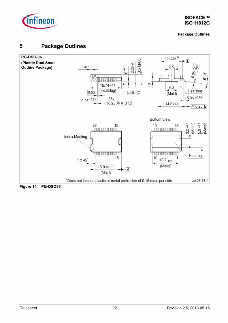
Datasheet 22 Revision 2.5, 2013-05-16
5 Package Outlines
Figure 14 PG-DSO36
Bottom View
Does not include plastic or metal protrusion of 0.15 max. per side
1 18
0.25
±0.11.1
36
+0.130.2536x
19
M
(Heatslug)15.74
0.65
±0.1
CA B
19
C
3.25
3.5
MA
X.
+0.1
0
0.1
±0.1
36
2.8B
11±0.15 1)
1.3
5˚0.25 ±3
˚
-0.0
2+0
.07
6.3
14.2
(Mold)
±0.3B
±0.15
0.25
Heatslug
0.95
Heatslug
±0.1
5.9
3.2
(Met
al)
±0.1
(Met
al)
13.7
(Metal)
10 1-0.2
Index Marking
(Mold)15.9 1)±0.1
A
1 x 45˚
1) gps09181_1
PG-DSO-36(Plastic Dual Small Outline Package)