
ISL99227, ISL99227B Datasheet - Renesas Electronics
17
FN8684 Rev.3.00 Oct 2, 2017 ISL99227, ISL99227B Smart Power Stage (SPS) Module with Integrated High Accuracy Current and Temperature Monitors DATASHEET FN8684 Rev.3.00 Page 1 of 17 Oct 2, 2017 The ISL99227 and ISL99227B are Smart Power Stage (SPS) compatible with Intersil’s ISL68xxx/69xxx Digital Multiphase (DMP) controllers and phase doubler (ISL6617A), respectively. The ISL99227 and ISL99227B have integrated high accuracy current and temperature monitors that can be fed back to the controller and doubler to complete a multiphase DC/DC system. They simplify design and increase performance by eliminating the DCR sensing network and associated thermal compensation. Light-load efficiency is supported through a dedicated LFET control pin. An industry leading thermally enhanced 5x5 PQFN package allows minimal overall PCB real estate. The ISL99227 and ISL99227B feature a 3.3V compatible, 5.0V compatible tri-state PWM input that, working together with Intersil’s multiphase PWM controllers, provide a robust solution in the event of abnormal operating conditions. The ISL99227 and ISL99227B also improve system performance and reliability with integrated fault protection of UVLO, over-temperature, and overcurrent. An open-drain fault reporting pin simplifies the handshake between SPS and Intersil controllers and can be used to disable the controller during start-up and fault conditions. Related Literature • For a full list of related documents, visit our website - ISL99227 , ISL99227B product pages Features • Input range: +4.5V to +18V • Supports 60A DC current • ISL99227 with 3.3V compatible tri-state PWM input • ISL99227B with 5.0V compatible tri-state PWM input • Downslope current sensing • ±3% accuracy current monitor (IMON) with REFIN input • 8mV/°C temperature monitor with OT flag • Dedicated low-side FET control input • Comprehensive fault protection for high system reliability - High-side FET short and overcurrent protection - Over-temperature protection - V CC and V IN Undervoltage Lockout (UVLO) • Open-drain fault reporting output • Up to 2MHz switching frequency • Pb-free (RoHS compliant), 32 Ld 5x5 PQFN Applications • High frequency and high efficiency VRM and VRD • Core, graphic, and memory regulators for microprocessors • High density VR for server, networking, and cloud computing • POL DC/DC converters and video gaming consoles FIGURE 1. ISL99227 SIMPLIFIED APPLICATION BLOCK DIAGRAM ISL68xxx/ ISL69xxx CONTROLLER PWM PHASE BOOT +5V EN TMON SHOOT- THROUGH PROTECTION SMART CONTROL VCC PVCC PVCC GND GND VIN +12V GND L OUT IMON REFIN CS#n CSRTN#n PWM TEMP FAULT# LGCTRL C OUT V OUT SW ISL99227
Transcript of ISL99227, ISL99227B Datasheet - Renesas Electronics

FN8684Rev.3.00
Oct 2, 2017
ISL99227, ISL99227BSmart Power Stage (SPS) Module with Integrated High Accuracy Current andTemperature Monitors
DATASHEET
The ISL99227 and ISL99227B are Smart Power Stage (SPS) compatible with Intersil’s ISL68xxx/69xxx Digital Multiphase (DMP) controllers and phase doubler (ISL6617A), respectively. The ISL99227 and ISL99227B have integrated high accuracy current and temperature monitors that can be fed back to the controller and doubler to complete a multiphase DC/DC system. They simplify design and increase performance by eliminating the DCR sensing network and associated thermal compensation. Light-load efficiency is supported through a dedicated LFET control pin. An industry leading thermally enhanced 5x5 PQFN package allows minimal overall PCB real estate.
The ISL99227 and ISL99227B feature a 3.3V compatible, 5.0V compatible tri-state PWM input that, working together with Intersil’s multiphase PWM controllers, provide a robust solution in the event of abnormal operating conditions. The ISL99227 and ISL99227B also improve system performance and reliability with integrated fault protection of UVLO, over-temperature, and overcurrent. An open-drain fault reporting pin simplifies the handshake between SPS and Intersil controllers and can be used to disable the controller during start-up and fault conditions.
Related Literature• For a full list of related documents, visit our website
- ISL99227, ISL99227B product pages
Features• Input range: +4.5V to +18V
• Supports 60A DC current
• ISL99227 with 3.3V compatible tri-state PWM input
• ISL99227B with 5.0V compatible tri-state PWM input
• Downslope current sensing
• ±3% accuracy current monitor (IMON) with REFIN input
• 8mV/°C temperature monitor with OT flag
• Dedicated low-side FET control input
• Comprehensive fault protection for high system reliability
- High-side FET short and overcurrent protection
- Over-temperature protection
- VCC and VIN Undervoltage Lockout (UVLO)
• Open-drain fault reporting output
• Up to 2MHz switching frequency
• Pb-free (RoHS compliant), 32 Ld 5x5 PQFN
Applications• High frequency and high efficiency VRM and VRD
• Core, graphic, and memory regulators for microprocessors
• High density VR for server, networking, and cloud computing
• POL DC/DC converters and video gaming consoles
FIGURE 1. ISL99227 SIMPLIFIED APPLICATION BLOCK DIAGRAM
ISL68xxx/ISL69xxx
CONTROLLER
PWM
PHASEBOOT
+5V
EN
TMON
SHOOT-THROUGH
PROTECTION
SMART CONTROL
VCC PVCC
PVCC
GND GND
VIN
+12V
GND
LOUTIMON
REFINCS#n
CSRTN#n
PWM
TEMPFAULT#
LGCTRL
COUT
VOUTSW
ISL99227
FN8684 Rev.3.00 Page 1 of 17Oct 2, 2017

ISL99227, ISL99227B
Typical Application Circuit with ISL99227
FIGURE 2. TYPICAL APPLICATION CIRCUIT WITH ISL99227 (ISL99227B 5V PWM IS NOT COMPATIBLE WITH ISL69127)
VCC
VSENVCORE
RGNDVCORE
VSA
ENVCORE
ISL69127
+3.3V
GND ADDRESS
VCCS
ENVSA
CONFIG
VCCS
VCORE
PGVCORE
VSENVSA
RGNDVSA
VCCS
CSRTNVSA
CSVSA
PWMVSA
TEMPVSA
ISL99227
PWM
IMON
REFIN
TMON
LGCTRL
SW
VIN VIN
VCC
BOOTFAULT#
5VPVCC
GND
5V
PHASE
CSRTN1
CS1
PWM1
TEMPVCORE
ISL99227
PWM
IMON
REFIN
TMON
LGCTRL
SW
VIN VIN
VCC
BOOTFAULT#
5VPVCC
GND
5V
PHASE
CSRTN2
CS2
PWM2
CS3-5
CSRTN3-5
PWM3-5
CSRTN6
CS6
PWM6
ISL99227
PWM
IMON
REFIN
TMON
LGCTRL
PHASE
VIN VIN
VCC
BOOTFAULT#
5VPVCC
GND
5V
SW
PMSDA
nPMALERT
PMSCL
SVDATA
SVCLK
nSVALERT
PGVSA
nVRHOT
nPINALERT
CFP
VINSEN
VIN
N PHASES
ISL99227
PWM
IMON
REFIN
TMON
LGCTRL
SW
VIN VIN
VCC
BOOTFAULT#
5VPVCC
GND
5V
PHASE
5V
5V
5V
5V
470pF
470pF
470pF
470pF
100
100
100
100
FN8684 Rev.3.00 Page 2 of 17Oct 2, 2017

ISL99227, ISL99227B
Typical Application Circuit with ISL99227B and ISL6617A
FIGURE 3. TYPICAL APPLICATION CIRCUIT WITH ISL99227B (COMPATIBLE WITH ISL6617A 5V PWM OUTPUT)
VCC
VSENVCORE
RGNDVCORE
ENVCORE
ISL69158
+3.3V
VCCS
VCCS
LOAD
CSRTN1
CS1
PWM1
TEMPVCORE
CS2-5
CSRTN2-5
PWM2-5
CSRTN6
CS6
PWM6
N Phases
ISL6617A
PWM
PWMB
CSENB
CSENA
CSRTNA
PWMA
CSRTNB
5V
ISL99227B
REFIN
TMON
FAULT#
IMON
LGCTRL
SW
VIN VIN
VCC
BOOTPWM
5VPVCC
GND
5V
PHASE
5V
ISL99227B
REFIN
TMON
FAULT#
IMON
LGCTRL
SW
VIN VIN
VCC
BOOTPWM
5VPVCC
GND
5V
PHASE
ISL6617A
PWM
PWMB
CSENB
CSENA
CSRTNA
PWMA
CSRTNB
5V
ISL99227B
REFIN
TMON
FAULT#
IMON
LGCTRL
SW
VIN VIN
VCC
BOOTPWM
5VPVCC
GND
5V
PHASE
ISL99227B
REFIN
TMON
FAULT#
IMON
LGCTRL
SW
VIN VIN
VCC
BOOTPWM
5VPVCC
GND
5V
PHASE
5V
VCCS
IOUT
IOUT
EN_SYNC
SYNC
5V
SYNC
SYNC
EN_SYNC
FN8684 Rev.3.00 Page 3 of 17Oct 2, 2017

ISL99227, ISL99227B
Functional Block Diagram
FIGURE 4. FUNCTIONAL BLOCK DIAGRAM
BOOT
VCC
PVCC
PVCC
VIN
20k
PWM
SW
GNDNC
PHASE
LGCTRL
FAULT#
GL
GH
OT
VCCPOR
16.5k
33.5k (for 3.3V)
2.5VLDO
HFET
LFET
VCC UVLO
+- PHASE
-+
100mV
GL
ORFUNCTION
VINPOR
V(TJ)
VIN UVLO
+-
90A
+-
OCH
+-
PWMH
PWML
VUGH
VLGH
OCH
VCCPOR
VINPOR
HS DRIVER
LS DRIVERAGND-PGND
LEVEL SHIFTER
TMON
OT
+-
V(TJ) V(TMAX) TEMP SENSE TJ
V (TJ) = 0.6V + 8mV * TJ 2.5V
2.5VCSH
GH_BLANK CONTROL
DEAD TIME AND SHOOT-THROUGH
LOGIC
VCC-BOOT LEVEL SHIFTER
GL_BLANK CONTROL
CSL REFIN
IMON
REFIN + 1.2V
OCH1µs PULSE
HFET SHORT
CAL
AND
LEVSHFT
PWM LOGIC
BOOT SWITCH
CONTROL
16.5k (for 5.0V)
+-
Ordering InformationPART NUMBER(Notes 1, 2, 3)
PARTMARKING
TEMP RANGE(°C)
CURRENTRATING
PWM INPUT(V)
TAPE AND REEL(UNITS)
PACKAGE(RoHS COMPLIANT)
PKG. DWG. #
ISL99227IRZ-T 27I -40 to +85 60A 3.3 3k 32 Ld 5x5 PQFN Double Cooling L32.5x5V
ISL99227HRZ-T 27H -10 to +100 60A 3.3 3k 32 Ld 5x5 PQFN Double Cooling L32.5x5V
ISL99227FRZ-T 27F -40 to +125 60A 3.3 3k 32 Ld 5x5 PQFN Double Cooling L32.5x5V
ISL99227BFRZ-T 27B -40 to +125 60A 5.0 3k 32 Ld 5x5 PQFN Double Cooling L32.5x5V
NOTES:
1. Refer to TB347 for details on reel specifications.
2. These Intersil plastic packaged products are RoHS compliant by EU exemption 7A and employ special Pb-free material sets, molding compounds/die attach materials, and 100% matte tin plate plus anneal (e3) termination finish which is compatible with both SnPb and Pb-free soldering operations. Intersil RoHS compliant products are MSL classified at Pb-free peak reflow temperatures that meet or exceed the Pb-free requirements of IPC/JEDEC J STD-020.
3. For Moisture Sensitivity Level (MSL), see the product information pages for ISL99227, ISL99227B. For more information on MSL, see Tech Brief TB363.
FN8684 Rev.3.00 Page 4 of 17Oct 2, 2017

ISL99227, ISL99227B
TABLE 1. KEY DIFFERENCES BETWEEN FAMILY OF PARTS
PART #
CURRENTRATING
(A)PWM
(V)THERMAL
FLAGOCPFLAG IMON TMON PACKAGE
P2PCOMPATIBLE USED WITH
5.0V PWM POWER STAGE FAMILY
ISL99125B 25 5.0 No No No No 24 Ld 3.5x5 QFN ISL99135B Analog Controllers: ISL633x, ISL636x, ISL637x, ISL95829, ISL9585xDigital Hybrid Controllers: ISL68201, ISL6388/98Full Digital Controller: ZL8802Phase Doublers: ISL6617, ISL6617A (see Figure 3 on page 3)
ISL99135B 35 5.0 No No No No 24 Ld 3.5x5 QFN ISL99125B
ISL99227B 60 5.0 Yes Yes Yes Yes 32 Ld 5x5 PQFN N/A
3.3V PWM POWER STAGE FAMILY
ISL99140 40 3.3 Yes No No No 40 Ld 6x6 QFN N/A Full Digital Controllers: ISL68/69xxx (see Figure 2 on page 2), ZL8802Digital Hybrid Controllers: ISL68201, ISL6388/98 (3.3V PWM Setting)
ISL99227 60 3.3 Yes Yes Yes Yes 32 Ld 5x5 PQFN N/A
Pin ConfigurationISL99227, ISL99227B
(32 LD PQFN)TOP VIEW
1
4
2
3
5
8
6
7
9 1110 12 13 14 15 16
17
18
19
20
21
22
23
32 3031 29 28 27 26 25 24
LGCTRL
VCC
PVCC
GND
NC
GND
GND
GND
GND
GND
GND
GND
VIN
VIN
VIN
SW SW SW SW SW SW SW SW
IMO
N
REF
IN
GN
D
PWM
VIN
FAUL
T#
BO
OT
PHA
SE
TMO
N
VIN34
GND35
GND33
FN8684 Rev.3.00 Page 5 of 17Oct 2, 2017

ISL99227, ISL99227B
Pin DescriptionsPIN # PIN NAME DESCRIPTION
1 LGCTRL Lower gate control signal input. LO = GL low (LFET off). HI = Normal operation (GL and GH strictly obey PWM). This pin should be driven with a logic signal, or externally tied high if not required; it should NOT be left floating.
2 VCC +5V logic bias supply. Place a high quality low ESR ceramic capacitor (~1µF/X7R) in close proximity from this pin to GND.
3 PVCC +5V gate drive bias supply. Place a high quality low ESR ceramic capacitor (~1µF/X7R) in close proximity from this pin to GND.
4, 6, 7, 8, 17, 18, 19, 20, 29
PAD 33, PAD 35
GND All GND pins are internally connected. Pins 4 and 29 should be connected directly to the nearby GND paddles on the package bottom. Figure 15 on page 14 shows GND paddles should be connected to the system GND plane with as many vias as possible to maximize thermal and electrical performance.
5 NC No connect (this is a low-side gate driver output (GL), optional to monitor for system debugging).
9, 10, 11, 12, 13, 14, 15, 16
SW Switching junction node between HFET source and LFET drain. Connect directly to output inductor.
21, 22, 23, 27, PAD 34
VIN Input of power stage (to drain of HFET). Place at least 2 ceramic capacitors (10µF or higher, X5R or X7R) in close proximity across VIN and GND. Pin 27 should NOT be used for decoupling. For optimal performance, place as many vias as possible in the bottom side VIN paddle.
24 PHASE Return of boot capacitor. Internally connected to SW node so no external routing required for SW connection.
25 BOOT Floating bootstrap supply pin for the upper gate drive. Place a high quality low ESR ceramic capacitor (0.1µF~0.22µF/X7R) in close proximity across BOOT and PHASE pins.
26 FAULT# Open-drain output pin. Any fault (overcurrent, over-temperature, shorted HFET, or POR/UVLO) will pull this pin to ground. This pin can be connected to the controller Enable pin or used to signal a fault at the system level.
28 PWM ISL99227: PWM input of gate driver, compatible with 3.3V tri-state PWM signal. ISL99227B for 5V PWM.
30 REFIN Input for external reference voltage for IMON signal. This voltage should be between 0.8V and 1.6V. Connect REFIN to the appropriate current sense input of the controller. Place a high quality low ESR ceramic capacitor (~ 0.1µF) in close proximity from this pin to GND.
31 IMON Current monitor output, referenced to REFIN. IMON will be pulled high (to REFIN + 1.2V) to indicate an HFET shorted or overcurrent fault. Connect the IMON output to the appropriate current sense input of the controller. No more than 56pF capacitance can be directly connected across IMON and REFIN pins. Typically, a 100Ω series resistor and 470pF is recommended.
32 TMON Temperature monitor output. For multiphase, the TMON pins can be connected together as a common bus; the highest voltage (representing the highest temperature) will be sent to the PWM controller. TMON will be pulled high (to 2.5V) to indicate an over-temperature fault. No more than 470pF total capacitance can be directly connected across the TMON and GND pins; with a series resistor, a higher capacitance load is allowed, such as 1kΩ for 100nF load.
FN8684 Rev.3.00 Page 6 of 17Oct 2, 2017

ISL99227, ISL99227B
Absolute Maximum Ratings Thermal InformationSupply Voltage (VCC, PVCC). . . . . . . . . . . . . . . . . . . . . . . . . . . . . . -0.3V to 6VInput Supply Voltage (VIN) . . . . . . . . . . . . . . . . . . . . . . . . . . . . . -0.3V to 25VPHASE, SW Voltage (VPH-GND, VSW-GND). . . . . . . . . . . . . . . . . . -0.3V to 25V
GND - 10V (<20ns Pulse Width, 10µJ)BOOT Voltage (VBOOT-GND) . . . . . . . . . . . . . . . . . . . . . . . . . . . . . -0.3V to 36VOther I/O Pin Voltage . . . . . . . . . . . . . . . . . . . . . . . . . . . -0.3V to VCC + 0.3VESD Ratings
Human Body Model (Tested per JEDEC-JS-001-2014) . . . . . . . . . . .2.5kVCharged Device Model (Tested per JS-002-2014) . . . . . . . . . . . . . . . 1kVMachine Model (Tested per JESD22-A115C) . . . . . . . . . . . . . . . . . 250V
Latch-Up (Tested per JESD-78E; Class 2, Level A). . . . . . . . . . . . . . . 100mA
Thermal Resistance JA (°C/W) JC (°C/W)32 Ld 5x5 PQFNDouble Cooling Package (Notes 4, 5, 7). . . . 10.7 4
Maximum Junction Temperature (Plastic Package) . . . . . . . . . . . .+150°CMaximum Storage Temperature Range . . . . . . . . . . . . . .-65°C to +150°CPb-Free Reflow Profile . . . . . . . . . . . . . . . . . . . . . . . . . . . . . . . . . . see TB493
Recommended Operating ConditionsOperating Junction Temperature Range
IRZ . . . . . . . . . . . . . . . . . . . . . . . . . . . . . . . . . . . . . . . . . . . . -40°C to +85°CHRZ. . . . . . . . . . . . . . . . . . . . . . . . . . . . . . . . . . . . . . . . . . .-10°C to +100°CFRZ . . . . . . . . . . . . . . . . . . . . . . . . . . . . . . . . . . . . . . . . . . .-40°C to +125°C
Supply Voltage, VCC, PVCC. . . . . . . . . . . . . . . . . . . . . . . . . . . . . . . . . . 5V ±5%Input Supply Voltage, VIN. . . . . . . . . . . . . . . . . . . . . . . . . . . . . . . 4.5V to 18V
CAUTION: Do not operate at or near the maximum ratings listed for extended periods of time. Exposure to such conditions may adversely impact productreliability and result in failures not covered by warranty.
NOTES:
4. JA is measured in free air with the component mounted on an Intersil SPS evaluation board. Refer to Tech Brief TB379 for general thermal metric info.
5. For JC, the “case temp” location is the center of the package underside.
Electrical Specifications Recommended operating conditions, unless otherwise noted. Boldface limits apply across the operating temperature range, TJ = -40°C to +125°C.
PARAMETER SYMBOL TEST CONDITIONSMIN
(Note 6) TYPMAX
(Note 6) UNIT
POWER RATING
Maximum Instant Power Dissipation TA = +25°C, 150A, (Note 7) 100 W
Maximum Continuous Power Dissipation TA = +25°C, JA= 10°C/W, TJ = +150°C, (Note 7) 12.5 W
THERMAL RESISTANCE
Thermal Resistance Junction to PCB JB Intersil SPS evaluation board, (Note 7) 5.2 °C/W
Thermal Resistance Junction to Ambient JA Intersil SPS evaluation board, (Note 7), 0 LFM 10.7 °C/W
Thermal Resistance Junction to Ambient JA Intersil SPS evaluation board, (Note 7), 400 LFM 9.3 °C/W
VCC SUPPLY CURRENT
Logic Standby Current IVCC PWM = Open 4.75 mA
Gate Drive Standby Current IPVCC PWM = Open 100 µA
Logic Operational Current IVCC PWM = 300kHz 4.75 mA
Gate Drive Operational Current IPVCC PWM = 300kHz 15 mA
POWER-ON RESET AND ENABLE
VCC Rising POR Threshold 3.86 4.20 V
VCC Falling POR Threshold 3.20 3.58 V
VCC POR Hysteresis 280 mV
VCC POR Delay to Operation 125 197 µs
VIN Rising POR Threshold 4.0 4.2 V
VIN Falling POR Threshold 3.4 3.5 V
VIN POR Hysteresis 445 mV
FN8684 Rev.3.00 Page 7 of 17Oct 2, 2017

ISL99227, ISL99227B
3.3V PWM INPUT FOR ISL99227 (See “TIMING DIAGRAM” Figure 5 on page 9)
Sink Impedance 33.5 kΩ
Source Impedance 16.5 kΩ
Tri-State Lower Gate Falling Threshold VCC = 5V 1.11 V
Tri-State Lower Gate Rising Threshold VCC = 5V 0.87 V
Tri-State Upper Gate Rising Threshold VCC = 5V 2.13 V
Tri-State Upper Gate Falling Threshold VCC = 5V 1.95 V
Tri-State Shutdown Window VCC = 5V 1.3 1.8 V
5V PWM INPUT FOR ISL99227B (See “TIMING DIAGRAM” on Figure 5 on page 9)
Sink Impedance 16.5 kΩ
Source Impedance 16.5 kΩ
Tri-State Lower Gate Falling Threshold VCC = 5V 1.51 V
Tri-State Lower Gate Rising Threshold VCC = 5V 1.14 V
Tri-State Upper Gate Rising Threshold VCC = 5V 3.24 V
Tri-State Upper Gate Falling Threshold VCC = 5V 3.02 V
Tri-State Shutdown Window VCC = 5V 1.6 2.8 V
SWITCHING TIME
GH Turn-On Propagation Delay tPDHU See Figure 5 (GL Low to GH High) 8 ns
GH Turn-Off Propagation Delay tPDLU See Figure 5 (PWM Low to GH Low) 40 ns
GL Turn-On Propagation Delay tPDHL See Figure 5 (GH Low to GL High) 8 ns
GL Turn-Off Propagation Delay tPDLL See Figure 5 (PWM High to GL Low) 23 ns
GL Exit Tri-State Propagation Delay tPDTSL See Figure 5 (Tri-state to GL High) 25 ns
GH Exit Tri-State Propagation Delay tPDTSU See Figure 5 (Tri-state to GH High) 35 ns
PWML to Tri-State Shutdown Hold-Off Time tTSSHDL See Figure 5 (PWM Low to GL Low) 40 ns
PWMH to Tri-State Shutdown Hold-Off Time tTSSHDU See Figure 5 (PWM High to GH Low) 50 ns
CURRENT MONITOR
REFIN Voltage Range 0.8 1.2 1.6 V
IMON Current Gain Accuracy(Intersil SPS Validation Board, VCC = 5V)
10A, TJ = +90°C ±2 %
≥10A, TJ = +40°C to +125°C ±3 %
≥10A, TJ = +20°C to +125°C ±4 %
Downslope Blanking Time 160 ns
HFET Overcurrent Trip VCC = 5V 90 A
IMON-REFIN at OCP 1.1 1.2 1.3 V
TEMPERATURE MONITOR
Over-Temperature Rising Threshold 140 °C
Over-Temperature Falling Threshold 125 °C
Over-Temperature Hysteresis 15 °C
Temperature Coefficient 8 mV/K
Electrical Specifications Recommended operating conditions, unless otherwise noted. Boldface limits apply across the operating temperature range, TJ = -40°C to +125°C. (Continued)
PARAMETER SYMBOL TEST CONDITIONSMIN
(Note 6) TYPMAX
(Note 6) UNIT
FN8684 Rev.3.00 Page 8 of 17Oct 2, 2017

ISL99227, ISL99227B
TMON Voltage at +25°C Temperature V (TJ) = 0.6V + (8mV*TJ) 0.80 V
TMON High at Over-Temperature 2.3 2.5 2.7 V
FAULT PIN
Output Low Voltage 5mA 0.18 0.26 V
Leakage Current 16 nA
BOOTSTRAP DIODE
Forward Voltage Drop 5mA 0.09 V
ON-Resistance RF 16 Ω
LGCTRL PIN
Rising Threshold Logic high; (Normal: obeys PWM) 1.29 1.60 V
Falling Threshold Logic low; (Forces GL low; LFET off) 0.70 1.01 V
MOSFETs
High-Side MOSFET (HFET) rDS(ON) 3.84 mΩ
Low-Side MOSFET (LFET) rDS(ON) 0.76 mΩ
NOTES:
6. Compliance to datasheet limits is assured by one or more methods: production test, characterization, and/or design.
7. These ratings vary with PCB layout and operating condition, and limited by SPS temperature and thermal shutdown trip point.
Electrical Specifications Recommended operating conditions, unless otherwise noted. Boldface limits apply across the operating temperature range, TJ = -40°C to +125°C. (Continued)
PARAMETER SYMBOL TEST CONDITIONSMIN
(Note 6) TYPMAX
(Note 6) UNIT
FIGURE 5. TIMING DIAGRAM (INTERNAL SIGNALS)
PWM
GH
GL
tFL
tPDHU
tPDLL
tRL
tTSSHDL
tPDTSL
tPDTSU
tFUtRU
tPDLU
tPDHL
tTSSHDU
tPDLFUR tPDUFLR
FN8684 Rev.3.00 Page 9 of 17Oct 2, 2017
ISL99227, ISL99227B
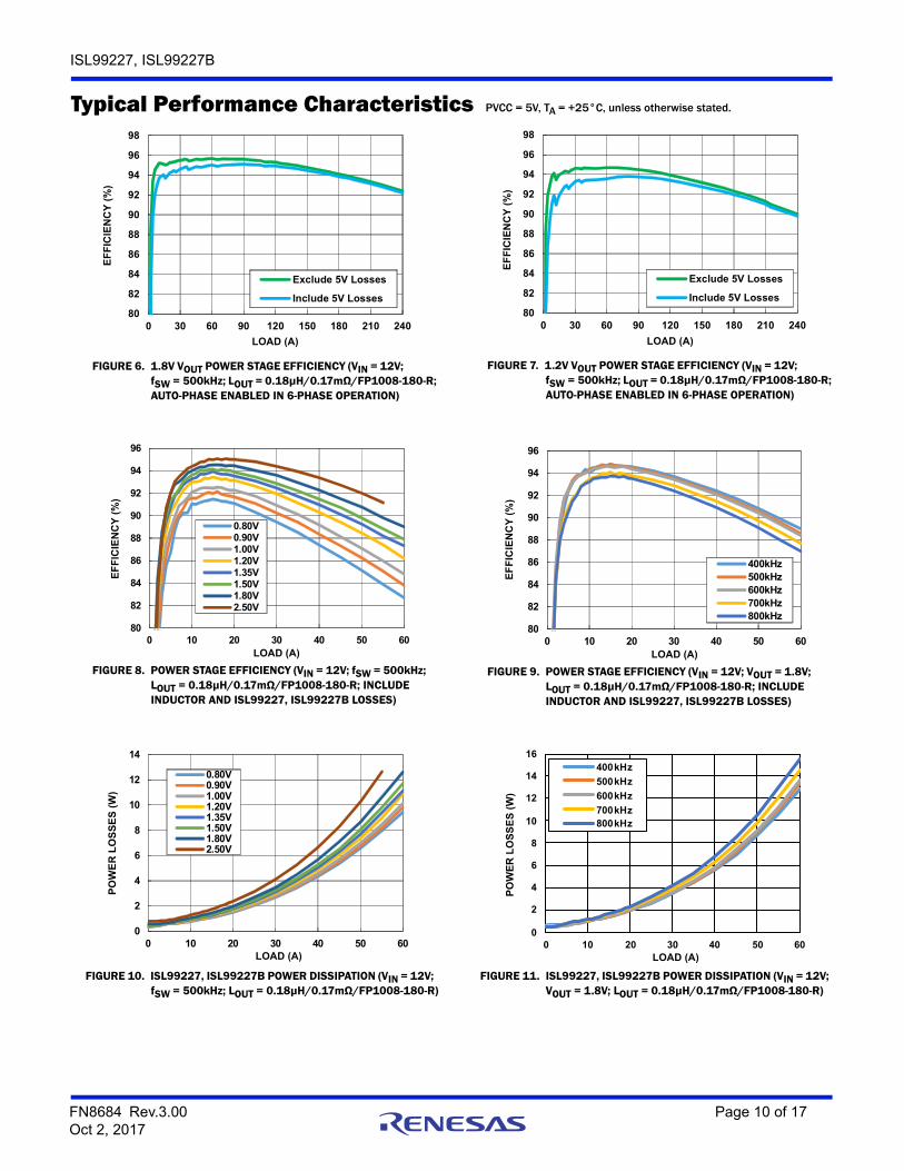
Typical Performance Characteristics PVCC = 5V, TA = +25°C, unless otherwise stated.
FIGURE 6. 1.8V VOUT POWER STAGE EFFICIENCY (VIN = 12V; fSW = 500kHz; LOUT = 0.18µH/0.17mΩ/FP1008-180-R; AUTO-PHASE ENABLED IN 6-PHASE OPERATION)
FIGURE 7. 1.2V VOUT POWER STAGE EFFICIENCY (VIN = 12V; fSW = 500kHz; LOUT = 0.18µH/0.17mΩ/FP1008-180-R; AUTO-PHASE ENABLED IN 6-PHASE OPERATION)
FIGURE 8. POWER STAGE EFFICIENCY (VIN = 12V; fSW = 500kHz; LOUT = 0.18µH/0.17mΩ/FP1008-180-R; INCLUDE INDUCTOR AND ISL99227, ISL99227B LOSSES)
FIGURE 9. POWER STAGE EFFICIENCY (VIN = 12V; VOUT = 1.8V; LOUT = 0.18µH/0.17mΩ/FP1008-180-R; INCLUDE INDUCTOR AND ISL99227, ISL99227B LOSSES)
FIGURE 10. ISL99227, ISL99227B POWER DISSIPATION (VIN = 12V; fSW = 500kHz; LOUT = 0.18µH/0.17mΩ/FP1008-180-R)
FIGURE 11. ISL99227, ISL99227B POWER DISSIPATION (VIN = 12V; VOUT = 1.8V; LOUT = 0.18µH/0.17mΩ/FP1008-180-R)
80
82
84
86
88
90
92
94
96
98
0 30 60 90 120 150 180 210 240
Exclude 5V Losses
Include 5V Losses
EF
FIC
IEN
CY
(%
)
LOAD (A)
80
82
84
86
88
90
92
94
96
98
0 30 60 90 120 150 180 210 240
Exclude 5V Losses
Include 5V Losses
EF
FIC
IEN
CY
(%
)
LOAD (A)
80
82
84
86
88
90
92
94
96
0 10 20 30 40 50 60
0.80V0.90V1.00V1.20V1.35V1.50V1.80V2.50V
EF
FIC
IEN
CY
(%
)
LOAD (A)
80
82
84
86
88
90
92
94
96
0 10 20 30 40 50 60
400kHz500kHz600kHz700kHz800kHz
LOAD (A)
EF
FIC
IEN
CY
(%
)
0
2
4
6
8
10
12
14
0 10 20 30 40 50 60
0.80V0.90V1.00V1.20V1.35V1.50V1.80V2.50V
PO
WE
R L
OS
SE
S (
W)
LOAD (A)
0
2
4
6
8
10
12
14
16
0 10 20 30 40 50 60
400kHz
500kHz
600kHz
700kHz800kHz
PO
WE
R L
OS
SE
S (
W)
LOAD (A)
FN8684 Rev.3.00 Page 10 of 17Oct 2, 2017

ISL99227, ISL99227B
Operation The ISL99227 and ISL99227B are optimized drivers and power stage solutions for high density synchronous DC/DC power conversion. They include high performance GH and GL drivers, an NFET controlled to function as a bootstrap diode, and a MOSFET pair optimized for high switching frequency buck voltage regulators. They also include advanced power management features listed as follows:
• Accurate current and thermal reporting outputs.
• Fault protections of HFET overcurrent, HFET short, over-temperature, VCC UVLO and VIN UVLO.
Power-On Reset (POR)During initial start-up, the VCC voltage rise is monitored. If the rising VCC voltage exceeds 3.86V (typical) for 125µs, then normal operation of the driver is enabled. The PWM signals are passed through to the gate drivers, the TMON output is valid and the IMON-REFIN output starts at zero, and becomes valid on the first GL signal. If VCC drops below the falling threshold of 3.58V (typical), operation of the driver is disabled. The PVCC voltage is not monitored because it should to be from the same supply as VCC.
VIN POR is also monitored. When both VCC and VIN reach above their POR trip points, it enables HFET overcurrent protection.
Both VCC and VIN POR are gated to the FAULT# pin, which goes high once both VCC and VIN are above their POR levels after 125µs and no other faults occur.
Shoot-Through ProtectionBefore POR, the undervoltage protection function is activated and both GH and GL are held active low (HFET and LFET off). After POR (the Rising Thresholds; see “Electrical Specifications” on page 8) and a 125µs delay, the PWM and LGCTRL signals are used to control both high-side and low-side MOSFETs, as shown in Table 2.
The ISL99227 and ISL99227B dead time control is optimized for high efficiency and guarantees that simultaneous conduction of both FETs cannot occur.
If the driver has no bias voltage applied (either VCC or PVCC missing) and is unable to actively hold the MOSFETs off, an integrated 20kΩ resistor from the upper MOSFET gate-to-source will aid in keeping the HFET device in its off state. This can be especially critical in applications where the input voltage rises before the ISL99227 and ISL99227B VCC and PVCC supplies.
Tri-State PWM InputThe ISL99227 supports a 3.3V PWM tri-level input and is compatible with Intersil’s digital multiphase controllers as well as other control ICs using 3.3V PWM logic. Use the ISL99227B for 5V PWM logic, like ISL6617A doubler with 5V PWM logic output (see Table 1 on page 5). If the pin is pulled into and remains in the tri-state window for a set hold-off time, the driver will force both MOSFETs to their off states. When the PWM signal moves outside the shutdown window, the driver immediately resumes driving the MOSFETs according to the PWM commands.
This feature is used by Intersil’s PWM controllers as a method of forcing both MOSFETs off. If the PWM input is left floating, the pin will be pulled into the tri-state window internally and thus force both MOSFETs to a safe off state.
Although the PWM input can sustain a voltage as high as VCC, the ISL99227 is not compatible with a controller (such as the ISL63xx family) that actively drives its mid-level in tri-state higher than 1.7V.
Bootstrap FunctionThe ISL99227 and ISL99227B feature an internal NFET that is controlled to function as a bootstrap diode. A high quality ceramic capacitor should be placed in close proximity across the BOOT and PHASE pins. The bootstrap capacitor can range between 0.1µF~0.22µF (0402~0603 and X5R~X7R) for normal buck switching applications.
Current MonitoringLFET current is monitored and a signal proportional to that current is the output on the IMON pin (relative to the REFIN pin). The IMON and REFIN pins should be connected to the appropriate current sense input pin of the controller. This method does not require external RSENSE or DCR sensing of the inductor current.
Figure 12 depicts the low-side current sense concept. After the falling edge of the PWM, there are two delays; one that represents the expected propagation delay from PWM to GH/SW and a second blanking delay to allow time for the transition to settle; typical total time is ~350ns. The IMON output approximates the actual IL waveform.
TABLE 2. GH AND GL OPERATION TRUTH TABLE
PWM LGCTRL GH GL HFET, LFET COMMENT
3-state X 0 0 Both off
0 1 0 1 LFET on Normal
1 1 1 0 HFET on Normal
0 0 0 0 LFET off GL low
1 0 1 0 HFET on Normal
FIGURE 12. LFET CURRENT SAMPLE DIAGRAM
ONdlyOFFdly
SW
GLGH
PWM
IL x IMONGAIN
IMON
FN8684 Rev.3.00 Page 11 of 17Oct 2, 2017

ISL99227, ISL99227B
The HFET current is NOT monitored in the same way, so no valid measured current is available while PWM is high (including the short delays before and after). During this time, the IMON will output the last valid LFET current before the sampling stopped. On start-up after POR, the IMON will output zero (relative to REFIN, which represents zero current) until the switching begins and then the current can be properly measured.
The high-side FET current is separately monitored for OC conditions; see the following “Overcurrent Protection” section.
Overcurrent ProtectionFigure 13 shows the timing diagram of an overcurrent fault. There is a comparator monitoring the HFET current while it is on (GH high; also requires VIN POR above its trip point). If the current is higher than 90A (typical; not user-programmable), then an OC fault is detected. The GH will be forced low, even if PWM is still high; this effectively shortens the PWM (and GH) pulse width, to limit the current. The IMON pin is pulled up to REFIN + 1.2V, which will be detected by the controller as an overcurrent fault. The controller is then expected to force PWM to tri-state (gates off both FETs), which signals the SPS that the fault has been acknowledged. The fault clears ~1µs after PWM enters tri-state. The IMON flag is released after the delay. The driver will then normally respond to the PWM inputs. If the PWM tri-state signal is not received after the fault, then the fault stays asserted and the IMON pin remains high.
Note that if the controller does NOT acknowledge, the IMON flag will stay high indefinitely, which will also hold GH low.
If OC is detected, the FAULT# pin is also pulled low; the timing on the FAULT# pin will follow that of the IMON pin.
Shorted HFET ProtectionIn case of a shorted HFET, the SW node will have excessive positive voltage present even when the LFET is turned on. The ISL99227 and ISL99227B monitor the SW node during periods when the LFET is on (GL is high) and should that voltage exceed 100mV (typical), the HFET short fault is declared. The ISL99227 and ISL99227B will pull the IMON pin high and the FAULT# will be pulled low. However, the fault will be latched; VCC POR is needed to reset it. GH will be gated low (ignore PWM = high), thus the ISL99227 and ISL99227B will still respond to PWM tri-state and logic low.
Thermal MonitoringThe ISL99227 and ISL99227B monitor their internal temperature and provides a signal proportional to that temperature on the TMON pin. TMON has a voltage of 600mV at 0°C and reflects temperature at 8mV/°C. The TMON output is valid 125µs after VCC POR.
Figure 14 shows a simplified functional representation. The top section includes the sensor and the output buffer. The bottom section includes the protection sensing that will pull the output high. The TMON pin is configured internally such that a user can tie multiple pins together externally and the resulting TMON bus will assume the voltage of the highest contributor (representing the highest temperature).
Thermal ProtectionIf the internal temperature exceeds the over-temperature trip point (+140°C typical), the TMON pin will be pulled high (to ~2.5V), and the FAULT# pin will be pulled low. No other action is taken on-chip. Both the TMON and FAULT# pins will remain in the fault mode until the junction temperature drops below +125°C (typical); at that point, the TMON and FAULT# pins resume normal operation.
FIGURE 13. OVERCURRENT FAULT TIMING DIAGRAM
ILIM
0
HFET
CURRENT
PWM
GH
GL
FAULT CLEAR DELAY 1µs
IMON - REFIN1.2V
RESUME NORMAL OP (IF RECOVERS)
FOLLOW PWM LOW TO SUPPORT OV FOLLOWING OC
NO GH ALLOWED
FAULT#
DMP ENTERS PWMMID-STATE TO ACKNOWLEDGE FAULT
FIGURE 14. OVER-TEMPERATURE FAULT
600mV+ 8mV/C* TEMP
TMON PIN
FAULT REPORTING
CONFIGURATION
OVER-TEMP
FN8684 Rev.3.00 Page 12 of 17Oct 2, 2017

ISL99227, ISL99227B
FAULT ReportingOvercurrent and shorted HFET detections will pull the IMON pin to a high (fault) level, so that the PWM controller should quickly recognize it as out of the normal range. Over-temperature detection will pull the TMON pin to a high (fault) level, so that the PWM controller should quickly recognize it as out of the normal range.
All of the above faults, plus the VCC and VIN POR (UVLO) conditions, will also pull down the FAULT# pin. This can be used by the controller (or system) as a fault detection and can also be used to disable the controller through its Enable pin.
The fault reporting and respective SPS response are summarized in Table 3.
PCB Layout ConsiderationsProper PCB layout will reduce noise coupling to other circuits, improve thermal performance and maximize the efficiency. The following is meant to lead to an optimized layout:
• Place multiple 10µF or greater ceramic capacitors directly on the device between VIN and GND as indicated in Figure 15 on page 14. This is the most critical decoupling and will reduce parasitic inductance in the power switching loop. This will reduce overall electrical stress on the device as well as reduce coupling to other circuits. Best practice is to place the decoupling capacitors on the same PCB side as the device. For a design with tight space requirements, these decoupling capacitors can be placed under the device, that is, bottom layer, as shown in Figure 17 on page 15.
• Connect GND to the system GND plane with a large via array as close to the GND pins as design rules allow. This improves thermal and electrical performance.
• Place PVCC, VCC, and BOOT-PHASE decoupling capacitors at the IC pins as shown in Figure 15 on page 14.
• Note that the SW plane connecting the ISL99227 and ISL99227B and inductor must carry full load current and will create resistive loss if not sized properly. However, it is also a very noisy node that should not be oversized or routed close to any sensitive signals. Best practice is to place the inductor as close to the device as possible and thus minimize the required area for the SW connection. If one must choose a long route of either the VOUT side of the inductor or the SW side, choose the quiet VOUT side. Best practice is to locate ISL99227 and ISL99227B as close to the final load as possible and thus avoid noisy or lossy routes to the load.
• The IMON and IREF network and their vias should not sit on the top of the VIN plane. A keep out area is recommended, as shown in Figure 17 on page 15.
• The PCB is a better thermal heatsink material than any top side cooling materials. The PCB always has enough vias to connect VIN and GND planes. Insufficient vias will yield lower efficiency and very poor thermal performance.
Figures 16 and 17 show a multiphase PCB layout example for dual footprint, a device compatible with ISL99227. For a reference design file, please contact Intersil’s Application support at www.intersil.com/en/support.html.
TABLE 3. FAULT REPORTING SUMMARY
FAULTEVENT IMON TMON FAULT# RESPONSE
OC HIGH N/A LOW GH gated off. The controller should acknowledge and force its PWM to tri-state to keep both HFET and LFET off. The fault is cleared ~1µs after PWM enters tri-state, otherwise, it stays asserted. (If system OVP occurs, the controller may send PWM low to turn on LFET).
ShortedHFET
IMON Latched
HIGH
N/A FAULT# Latched
LOW
GH gated off, until fault latch is cleared by VCC POR. GL follows PWM.
OT N/A HIGH LOW GH and GL follow PWM.
VCCUVLO
IMON-REFIN =
0V
TMONNot
Valid
LOW Switching stops while in UVLO. Once above VCC POR, after 125µs: GH and GL follow PWM; the FAULT# pin is released; TMON is valid; IMON-REFIN is valid after GL first goes low.
VINUVLO
OC not valid
N/A LOW GH and GL follow PWM.
FN8684 Rev.3.00 Page 13 of 17Oct 2, 2017

ISL99227, ISL99227B
TABLE 4. AVAILABLE EVALUATION BOARDS
EVALUATION BOARDSPEAK EFFICIENCY
(%)SMBus/
PMBus/I2C DESCRIPTION
ISL69127-61P-EV1Z 95.7% at 60A Yes 6+1 Dual Output VR13 Evaluation Board for VCORE and VSA Applications
ISL69125-31P-EV2Z 94.5% at 30A Yes 3+1 Dual Outputs DDR4 Evaluation Board for VR13 Memory Applications
FIGURE 15. SINGLE-PHASE PCB LAYOUT FOR MINIMIZING CURRENT LOOPS
FN8684 Rev.3.00 Page 14 of 17Oct 2, 2017

ISL99227, ISL99227B
FIGURE 16. MULTIPHASE PCB LAYOUT EXAMPLE TOP LAYER FOR DUAL FOOTPRINT, A DEVICE COMPATIBLE WITH ISL99227
FIGURE 17. MULTIPHASE PCB LAYOUT EXAMPLE BOTTOM LAYER
VIN DECOUPLING CAPACITORS
FN8684 Rev.3.00 Page 15 of 17Oct 2, 2017

ISL99227, ISL99227B
Intersil products are manufactured, assembled and tested utilizing ISO9001 quality systems as notedin the quality certifications found at www.intersil.com/en/support/qualandreliability.html
Intersil products are sold by description only. Intersil may modify the circuit design and/or specifications of products at any time without notice, provided that such modification does not, in Intersil's sole judgment, affect the form, fit or function of the product. Accordingly, the reader is cautioned to verify that datasheets are current before placing orders. Information furnished by Intersil is believed to be accurate and reliable. However, no responsibility is assumed by Intersil or its subsidiaries for its use; nor for any infringements of patents or other rights of third parties which may result from its use. No license is granted by implication or otherwise under any patent or patent rights of Intersil or its subsidiaries.
For information regarding Intersil Corporation and its products, see www.intersil.com
For additional products, see www.intersil.com/en/products.html
© Copyright Intersil Americas LLC 2016-2017. All Rights Reserved.All trademarks and registered trademarks are the property of their respective owners.
About IntersilIntersil Corporation is a leading provider of innovative power management and precision analog solutions. The company's products address some of the largest markets within the industrial and infrastructure, mobile computing and high-end consumer markets.
For the most updated datasheet, application notes, related documentation and related parts, please see the respective product information page found at www.intersil.com.
For a listing of definitions and abbreviations of common terms used in our documents, visit www.intersil.com/glossary.
You can report errors or suggestions for improving this datasheet by visiting www.intersil.com/ask.
Reliability reports are also available from our website at www.intersil.com/support.
Revision History The revision history provided is for informational purposes only and is believed to be accurate, but not warranted. Please go to the web to make sure that you have the latest revision.
DATE REVISION CHANGE
Oct 2, 2017 FN8684.3 Updated Related Literature section.Updated IMON pin description (last sentence).Updated Figure 2.Updated Figure 3.Added “Pad” to 33, 34, and 35 in the pin descriptions numbering.Updated About Intersil verbiage.Updated POD to the latest revision. Changes are as follows:
-Added dimensions to Bottom View (0.20, 0.20, 1.15, 0.95)
Oct 27, 2016 FN8684.2 Updated Ordering Information table on page 5 to show all Released parts.Added “for dual footprint, a device compatible with ISL99227” on page 13.Updated Figures 16 and 17 for dual footprint on page 15.
Sept 28, 2016 FN8684.1 Updated POD to revision 2 which added additional dimensions to the typical recommended land pattern and bottom views, and eliminated Note 6 which repeated the sentiments in the first line of Note 5.
Aug 30, 2016 FN8684.0 Initial Release
© Copyright Intersil Americas LLC 2016-2017. All Rights Reserved.All trademarks and registered trademarks are the property of their respective owners.
FN8684 Rev.3.00 Page 16 of 17Oct 2, 2017

ISL99227, ISL99227B
FN8684 Rev.3.00 Page 17 of 17Oct 2, 2017
Package Outline DrawingL32.5x5V32 LEAD DOUBLE COOLING QUAD FLAT NO-LEAD PLASTIC PACKAGE Rev 3 9/17
For the most recent package outline drawing, see L32.5x5V.