ISD2532 Datasheet Rev 1.2 - Digi-Key Sheets/Nuvoton PDFs/ISD2532,40... · v pd ovf p/r ce eom cca...
41
Publication Release Date: April 24, 2006 - 1 - Revision 1.2 ISD2532/40/48/64 SINGLE-CHIP, MULTIPLE-MESSAGES, VOICE RECORD/PLAYBACK DEVICE 32-, 40-, 48-, AND 64-SECOND DURATION
Transcript of ISD2532 Datasheet Rev 1.2 - Digi-Key Sheets/Nuvoton PDFs/ISD2532,40... · v pd ovf p/r ce eom cca...

Publication Release Date: April 24, 2006 - 1 - Revision 1.2
ISD2532/40/48/64
SINGLE-CHIP, MULTIPLE-MESSAGES,
VOICE RECORD/PLAYBACK DEVICE
32-, 40-, 48-, AND 64-SECOND DURATION
ISD2532/40/48/64
- 2 -
1. GENERAL DESCRIPTION Winbond’s ISD2500 ChipCorder® Series provide high-quality, single-chip, Record/Playback solutions for 32- to 64-second messaging applications. The CMOS devices include an on-chip oscillator, microphone preamplifier, automatic gain control, antialiasing filter, smoothing filter, speaker amplifier, and high density multi-level storage array. In addition, the ISD2500 is microcontroller compatible, allowing complex messaging and addressing to be achieved. Recordings are stored into on-chip nonvolatile memory cells, providing zero-power message storage. This unique, single-chip solution is made possible through Winbond’s patented multilevel storage technology. Voice and audio signals are stored directly into memory in their natural form, providing high-quality, solid-state voice reproduction.
2. FEATURES • Single 5 volt power supply • Single-chip with duration of 32, 40, 48, or 64 seconds. • Easy-to-use single-chip, voice record/playback solution • High-quality, natural voice/audio reproduction • Manual switch or microcontroller compatible • Playback can be edge- or level-activated • Directly cascadable for longer durations • Automatic power-down (push-button mode) - Standby current 1 µA (typical) • Zero-power message storage - Eliminates battery backup circuits • Fully addressable to handle multiple messages • 100-year message retention (typical) • 100,000 record cycles (typical) • On-chip clock source • Programmer support for play-only applications • Available in die form, PDIP and SOIC packaged units • Packaged type: leaded and lead-free
• Temperature options: die (0°C to +50°C) and package (0°C to +70°C)
ISD2532/40/48/64
Publication Release Date: April 24, 2006 - 3 - Revision 1.2
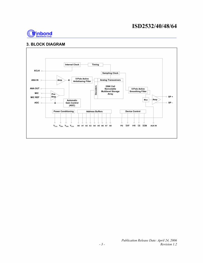
3. BLOCK DIAGRAM
Internal Clock Timing
Sampling Clock
256K CellNonvolatile
Multilevel StorageArray
Analog Transceivers
Dec
oder
s
Device ControlPower Conditioning
AutomaticGain Control
(AGC)
5-Pole ActiveAntialiasing Filter
5-Pole ActiveSmoothing Filter
Amp
Pre-Amp SP +
SP -
EOMCEP/ROVFPDVCCA VSSA VSSD VCCD
AGC
MIC REF
MIC
XCLK
AmpANA IN
ANA OUT
Mux
AUX IN
Address Buffers
A0 A1 A2 A3 A4 A5 A6 A7 A8

ISD2532/40/48/64
- 4 -
4. TABLE OF CONTENTS
1. GENERAL DESCRIPTION.................................................................................................................. 2
2. FEATURES ......................................................................................................................................... 2
3. BLOCK DIAGRAM .............................................................................................................................. 3
4. TABLE OF CONTENTS ...................................................................................................................... 4
5. PIN CONFIGURATION ....................................................................................................................... 5
6. PIN DESCRIPTION............................................................................................................................. 6
7. FUNCTIONAL DESCRIPTION.......................................................................................................... 10
7.1. Detailed Description.................................................................................................................... 10 7.2. Operational Modes ..................................................................................................................... 11
7.2.1. Operational Modes Description............................................................................................ 12
8. TIMING DIAGRAMS.......................................................................................................................... 16
9. ABSOLUTE MAXIMUM RATINGS.................................................................................................... 19
9.1 Operating Conditions ................................................................................................................... 20
10. ELECTRICAL CHARACTERISTICS ............................................................................................... 21
10.1. Parameters For Packaged Parts .............................................................................................. 21 10.1.1. Typical Parameter Variation with Voltage and Temperature - Packaged Parts ................ 24
10.2. Parameters For Die .................................................................................................................. 25 10.2.1. Typical Parameter Variation with Voltage and Temperature - Die .................................... 28
10.3. Parameters For Push-Button Mode.......................................................................................... 29
11. TYPICAL APPLICATION CIRCUIT................................................................................................. 30
12. PACKAGE DRAWING AND DIMENSIONS.................................................................................... 35
12.1. 28-Lead 300-Mil Plastic Small Outline IC (SOIC)..................................................................... 35 12.2. 28-Lead 600-Mil Plastic Dual Inline Package (PDIP) ............................................................... 36 12.3. Die Bonding Physical Layout [1] ................................................................................................ 37
13. ORDERING INFORMATION........................................................................................................... 39
14. VERSION HISTORY ....................................................................................................................... 40

ISD2532/40/48/64
Publication Release Date: April 24, 2006 - 5 - Revision 1.2
5. PIN CONFIGURATION
SOIC/PDIP
A0/M0
A1/M1
A2/M2
A3/M3
A4/M4
A5/M5
A6/M6
NC
A7
A8
AUX IN
VSSD
VSSA
SP +
P/R
XCLK
EOM
PD
CE
OVF
ANA OUT
ANA IN
AGC
MIC REF
MIC
VCCA
SP-
VCCD28
27
26
25
24
23
22
21
20
19
18
17
16
15
1
2
3
4
5
6
7
8
9
10
11
12
13
14
ISD2532ISD2540ISD2548ISD2564
ISD2532/40/48/64
- 6 -
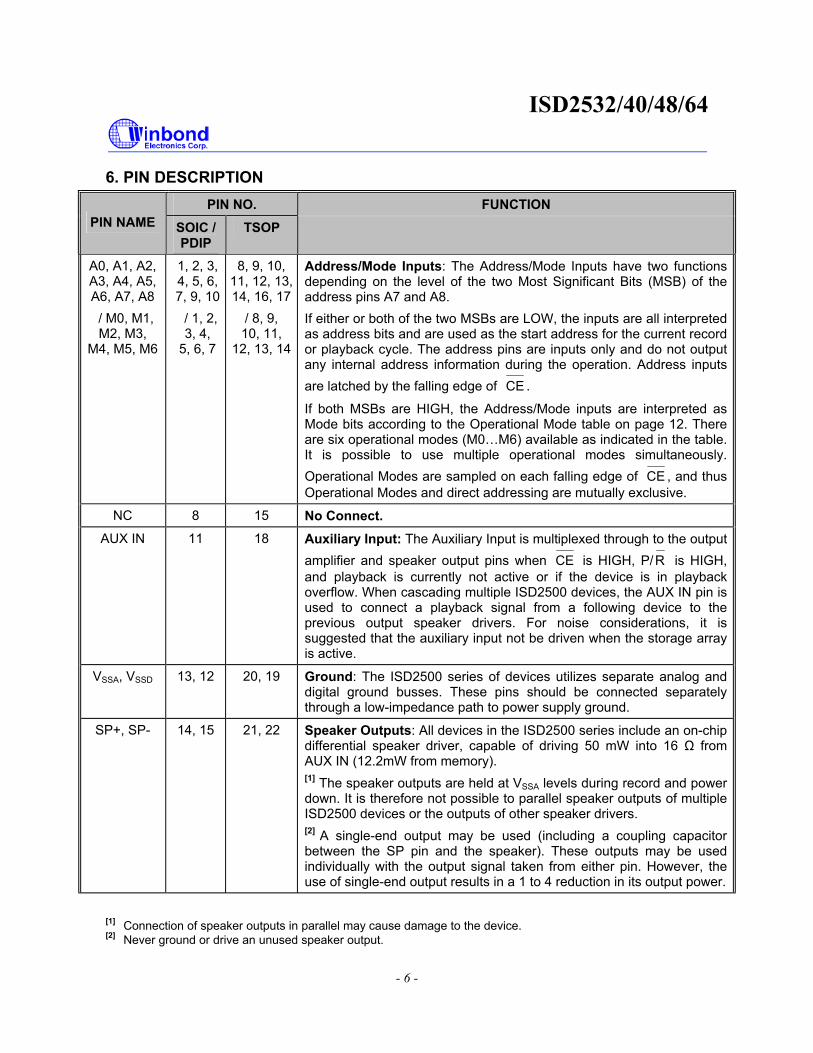
6. PIN DESCRIPTION PIN NO. FUNCTION
PIN NAME SOIC / PDIP
TSOP
A0, A1, A2, A3, A4, A5, A6, A7, A8 / M0, M1, M2, M3,
M4, M5, M6
1, 2, 3, 4, 5, 6, 7, 9, 10 / 1, 2, 3, 4,
5, 6, 7
8, 9, 10, 11, 12, 13, 14, 16, 17
/ 8, 9, 10, 11,
12, 13, 14
Address/Mode Inputs: The Address/Mode Inputs have two functions depending on the level of the two Most Significant Bits (MSB) of the address pins A7 and A8. If either or both of the two MSBs are LOW, the inputs are all interpreted as address bits and are used as the start address for the current record or playback cycle. The address pins are inputs only and do not output any internal address information during the operation. Address inputs are latched by the falling edge of CE .
If both MSBs are HIGH, the Address/Mode inputs are interpreted as Mode bits according to the Operational Mode table on page 12. There are six operational modes (M0…M6) available as indicated in the table. It is possible to use multiple operational modes simultaneously. Operational Modes are sampled on each falling edge of CE , and thus Operational Modes and direct addressing are mutually exclusive.
NC 8 15 No Connect. AUX IN 11 18 Auxiliary Input: The Auxiliary Input is multiplexed through to the output
amplifier and speaker output pins when CE is HIGH, P/R is HIGH, and playback is currently not active or if the device is in playback overflow. When cascading multiple ISD2500 devices, the AUX IN pin is used to connect a playback signal from a following device to the previous output speaker drivers. For noise considerations, it is suggested that the auxiliary input not be driven when the storage array is active.
VSSA, VSSD 13, 12 20, 19 Ground: The ISD2500 series of devices utilizes separate analog and digital ground busses. These pins should be connected separately through a low-impedance path to power supply ground.
SP+, SP- 14, 15 21, 22 Speaker Outputs: All devices in the ISD2500 series include an on-chip differential speaker driver, capable of driving 50 mW into 16 Ω from AUX IN (12.2mW from memory). [1] The speaker outputs are held at VSSA levels during record and power down. It is therefore not possible to parallel speaker outputs of multiple ISD2500 devices or the outputs of other speaker drivers. [2] A single-end output may be used (including a coupling capacitor between the SP pin and the speaker). These outputs may be used individually with the output signal taken from either pin. However, the use of single-end output results in a 1 to 4 reduction in its output power.
[1] Connection of speaker outputs in parallel may cause damage to the device. [2] Never ground or drive an unused speaker output.

ISD2532/40/48/64
Publication Release Date: April 24, 2006 - 7 - Revision 1.2
PIN NO.
PIN NAME SOIC/PDIP
TSOP FUNCTION
VCCA, VCCD 16, 28 23, 7 Supply Voltage: To minimize noise, the analog and digital circuits in the ISD2500 series devices use separate power busses. These voltage busses are brought out to separate pins and should be tied together as close to the supply as possible. In addition, these supplies should be decoupled as close to the package as possible.
MIC 17 24 Microphone: The microphone pin transfers input signal to the on-chip preamplifier. A built-in Automatic Gain Control (AGC) circuit controls the gain of this preamplifier from –15 to 24dB. An external microphone should be AC coupled to this pin via a series capacitor. The capacitor value, together with the internal 10 KΩ resistance on this pin, determines the low-frequency cutoff for the ISD2500 series passband. See Winbond’s Application Information for additional information on low-frequency cutoff calculation.
MIC REF 18 25 Microphone Reference: The MIC REF input is the inverting input to the microphone preamplifier. This provides a noise-canceling or common-mode rejection input to the device when connected to a differential microphone.
AGC 19 26 Automatic Gain Control: The AGC dynamically adjusts the gain of the preamplifier to compensate for the wide range of microphone input levels. The AGC allows the full range of whispers to loud sounds to be recorded with minimal distortion. The “attack” time is determined by the time constant of a 5 KΩ internal resistance and an external capacitor (C2 on the schematic of Figure 5 in section 11) connected from the AGC pin to VSSA analog ground. The “release” time is determined by the time constant of an external resistor (R2) and an external capacitor (C2) connected in parallel between the AGC pin and VSSA analog ground. Nominal values of 470 KΩ and 4.7 µF give satisfactory results in most cases.
ANA IN 20 27 Analog Input: The analog input transfers analog signal to the chip for recording. For microphone inputs, the ANA OUT pin should be connected via an external capacitor to the ANA IN pin. This capacitor value, together with the 3.0 KΩ input impedance of ANA IN, is selected to give additional cutoff at the low-frequency end of the voice passband. If the desired input is derived from a source other than a microphone, the signal can be fed, capacitively coupled, into the ANA IN pin directly.
ISD2532/40/48/64
- 8 -
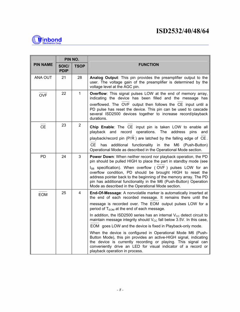
PIN NO. PIN NAME SOIC/
PDIP TSOP FUNCTION
ANA OUT 21 28 Analog Output: This pin provides the preamplifier output to the user. The voltage gain of the preamplifier is determined by the voltage level at the AGC pin.
OVF 22 1 Overflow: This signal pulses LOW at the end of memory array, indicating the device has been filled and the message has overflowed. The OVF output then follows the CE input until a PD pulse has reset the device. This pin can be used to cascade several ISD2500 devices together to increase record/playback durations.
CE 23 2 Chip Enable: The CE input pin is taken LOW to enable all playback and record operations. The address pins and playback/record pin (P/R ) are latched by the falling edge of CE .
CE has additional functionality in the M6 (Push-Button) Operational Mode as described in the Operational Mode section.
PD 24 3 Power Down: When neither record nor playback operation, the PD pin should be pulled HIGH to place the part in standby mode (see ISB specification). When overflow ( OVF ) pulses LOW for an overflow condition, PD should be brought HIGH to reset the address pointer back to the beginning of the memory array. The PD pin has additional functionality in the M6 (Push-Button) Operation Mode as described in the Operational Mode section.
EOM 25 4 End-Of-Message: A nonvolatile marker is automatically inserted at the end of each recorded message. It remains there until the message is recorded over. The EOM output pulses LOW for a period of TEOM at the end of each message. In addition, the ISD2500 series has an internal VCC detect circuit to maintain message integrity should VCC fall below 3.5V. In this case, EOM goes LOW and the device is fixed in Playback-only mode.
When the device is configured in Operational Mode M6 (Push-Button Mode), this pin provides an active-HIGH signal, indicating the device is currently recording or playing. This signal can conveniently drive an LED for visual indicator of a record or playback operation in process.

ISD2532/40/48/64
Publication Release Date: April 24, 2006 - 9 - Revision 1.2
PIN NO. PIN NAME SOIC/
PDIP TSOP FUNCTION
XCLK 26 5 External Clock: The external clock input has an internal pull-down device. The device is configured at the factory with an internal sampling clock frequency centered to ±1 percent of specification. The frequency is then maintained to a variation of ±2.25 percent over the entire commercial temperature and operating voltage ranges. If greater precision is required, the device can be clocked through the XCLK pin as follows:
Part Number Sample Rate Required Clock
ISD2532 8.0 kHz 1024 kHz
ISD2540 6.4 kHz 819.2 kHz
ISD2548 5.3 kHz 682.7 kHz
ISD2564 4.0 kHz 512 kHz
These recommended clock rates should not be varied because the antialiasing and smoothing filters are fixed, and aliasing problems can occur if the sample rate differs from the one recommended. The duty cycle on the input clock is not critical, as the clock is immediately divided by two. If the XCLK is not used, this input must be connected to ground.
P/R 27 6 Playback/Record: The P/R input pin is latched by the falling edge of the CE pin. A HIGH level selects a playback cycle while a LOW level selects a record cycle. For a record cycle, the address pins provide the starting address and recording continues until PD or CE is pulled HIGH or an overflow is detected (i.e. the chip is full).
When a record cycle is terminated by pulling PD or CE HIGH,
then End-Of-Message ( EOM ) marker is stored at the current address in memory. For a playback cycle, the address inputs provide the starting address and the device will play until an EOM
marker is encountered. The device can continue to pass an EOM
marker if CE is held LOW in address mode, or in an Operational Mode. (See Operational Modes section)
ISD2532/40/48/64
- 10 -
7. FUNCTIONAL DESCRIPTION
7.1. DETAILED DESCRIPTION
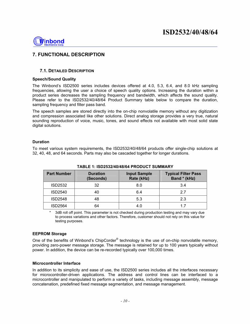
Speech/Sound Quality The Winbond’s ISD2500 series includes devices offered at 4.0, 5.3, 6.4, and 8.0 kHz sampling frequencies, allowing the user a choice of speech quality options. Increasing the duration within a product series decreases the sampling frequency and bandwidth, which affects the sound quality. Please refer to the ISD2532/40/48/64 Product Summary table below to compare the duration, sampling frequency and filter pass band. The speech samples are stored directly into the on-chip nonvolatile memory without any digitization and compression associated like other solutions. Direct analog storage provides a very true, natural sounding reproduction of voice, music, tones, and sound effects not available with most solid state digital solutions.
Duration To meet various system requirements, the ISD2532/40/48/64 products offer single-chip solutions at 32, 40, 48, and 64 seconds. Parts may also be cascaded together for longer durations.
TABLE 1: ISD2532/40/48/64 PRODUCT SUMMARY Part Number Duration
(Seconds) Input Sample
Rate (kHz) Typical Filter Pass
Band * (kHz) ISD2532 32 8.0 3.4
ISD2540 40 6.4 2.7
ISD2548 48 5.3 2.3
ISD2564 64 4.0 1.7 * 3dB roll off point. This parameter is not checked during production testing and may vary due
to process variations and other factors. Therefore, customer should not rely on this value for testing purposes.
EEPROM Storage One of the benefits of Winbond’s ChipCorder® technology is the use of on-chip nonvolatile memory, providing zero-power message storage. The message is retained for up to 100 years typically without power. In addition, the device can be re-recorded typically over 100,000 times. Microcontroller Interface In addition to its simplicity and ease of use, the ISD2500 series includes all the interfaces necessary for microcontroller-driven applications. The address and control lines can be interfaced to a microcontroller and manipulated to perform a variety of tasks, including message assembly, message concatenation, predefined fixed message segmentation, and message management.

ISD2532/40/48/64
Publication Release Date: April 24, 2006 - 11 - Revision 1.2
Programming The ISD2500 series is also ideal for playback-only applications, where single or multiple messages are referenced through buttons, switches, or a microcontroller. Once the desired message configuration is created, duplicates can easily be generated via a gang programmer.
7.2. OPERATIONAL MODES
The ISD2500 series is designed with several built-in Operational Modes that provide maximum functionality with minimum external components. These modes are described in details as below. The Operational Modes are accessed via the address pins and mapped beyond the normal message address range. When the two Most Significant Bits (MSB), A7 and A8, are HIGH, the remaining address signals are interpreted as mode bits and not as address bits. Therefore, Operational Modes and direct addressing are not compatible and cannot be used simultaneously. There are two important considerations for using Operational Modes. First, all operations begin initially at address 0 of its memory. Later operations can begin at other address locations, depending on the Operational Mode(s) chosen. In addition, the address pointer is reset to 0 when the device is changed from record to playback, playback to record (except M6 mode), or when a Power-Down cycle is executed.
Second, Operational Modes are executed when CE goes LOW. This Operational Mode remains in
effect until the next LOW-going CE signal, at which point the current mode(s) are sampled and executed.
TABLE 2: OPERATIONAL MODES Mode [1] Function Typical Use Jointly Compatible [2]
M0 Message cueing Fast-forward through messages M4, M5, M6
M1 Delete EOM markers Position EOM marker at the end of the last message
M3, M4, M5, M6
M2 Not applicable Reserved N/A
M3 Looping Continuous playback from Address 0 M1, M5, M6
M4 Consecutive addressing
Record/playback multiple consecutive messages
M0, M1, M5
M5 CE level-activated Allows message pausing M0, M1, M3, M4
M6 Push-button control Simplified device interface M0, M1, M3
[1] Besides mode pin needed to be “1”, A7 and A8 pin are also required to be “1” in order to enter into the related operational mode.
[2] Indicates additional Operational Modes which can be used simultaneously with the given mode.

ISD2532/40/48/64
- 12 -
7.2.1. Operational Modes Description The Operational Modes can be used in conjunction with a microcontroller, or they can be hardwired to provide the desired system operation.
M0 – Message Cueing Message Cueing allows the user to skip through messages, without knowing the actual physical addresses of each message. Each CE LOW pulse causes the internal address pointer to skip to the next message. This mode is used for playback only, and is typically used with the M4 Operational Mode.
M1 – Delete EOM Markers The M1 Operational Mode allows sequentially recorded messages to be combined into a single message with only one EOM marker set at the end of the final message. When this Operational Mode is configured, messages recorded sequentially are played back as one continuous message. M2 – Unused When Operational Modes are selected, the M2 pin should be LOW. M3 – Message Looping The M3 Operational Mode allows for the automatic, continuously repeated playback of the message located at the beginning of the address space. A message can completely fill the ISD2500 device and will loop from beginning to end without OVF going LOW.
M4 – Consecutive Addressing
During normal operation, the address pointer will reset when a message is played through an EOM
marker. The M4 Operational Mode inhibits the address pointer reset on EOM , allowing messages to be played back consecutively.
M5 - CE -Level Activated
The default mode for ISD2500 devices is for CE to be edge-activated on playback and level-
activated on record. The M5 Operational Mode causes the CE pin to be interpreted as level-activated as opposed to edge-activated during playback. This is especially useful for terminating playback operations using the CE signal. In this mode, CE LOW begins a playback cycle, at the
beginning of the device memory. The playback cycle continues as long as CE is held LOW. When
CE goes HIGH, playback will immediately end. A new CE LOW will restart the message from the beginning unless M4 is also HIGH.

ISD2532/40/48/64
Publication Release Date: April 24, 2006 - 13 - Revision 1.2
M6 – Push-Button Mode The ISD2500 series contain a Push-Button Operational Mode. The Push-Button Mode is used primarily in very low-cost applications and is designed to minimize external circuitry and components, thereby reducing system cost. In order to configure the device in Push-Button Operational Mode, the two most significant address bits must be HIGH, and the M6 mode pin must also be HIGH. A device in this mode always powers down at the end of each playback or record cycle after CE goes HIGH.
When this operational mode is implemented, three of the pins on the device have alternate functionality as described in the table below.
TABLE 3: ALTERNATE FUNCTIONALITY IN PINS Pin Name Alternate Functionality in Push-Button Mode
CE Start/Pause Push-Button (LOW pulse-activated)
PD Stop/Reset Push-Button (HIGH pulse-activated)
EOM Active-HIGH Run Indicator
CE (START/PAUSE)
In Push-Button Operational Mode, CE acts as a LOW-going pulse-activated START/PAUSE signal. If no operation is currently in progress, a LOW-going pulse on this signal will initiate a playback or record cycle according to the level on the P/R pin. A subsequent pulse on the CE pin, before an
EOM is reached in playback or an overflow condition occurs, will pause the current operation, and
the address counter is not reset. Another CE pulse will cause the device to continue the operation from the place where it is paused. PD (STOP/RESET)
In Push-Button Operational Mode, PD acts as a HIGH-going pulse-activated STOP/RESET signal. When a playback or record cycle is in progress and a HIGH-going pulse is observed on PD, the current cycle is terminated and the address pointer is reset to address 0, the beginning of the message space.
EOM (RUN)
In Push-Button Operational Mode, EOM becomes an active-HIGH RUN signal which can be used to drive an LED or other external device. It is HIGH whenever a record or playback operation is in progress. Recording in Push-Button Mode
1. The PD pin should be LOW, usually using a pull-down resistor.
ISD2532/40/48/64
- 14 -
2. The P/R pin is taken LOW.
3. The CE pin is pulsed LOW. Recording starts, EOM goes HIGH to indicate an operation in progress.
4. When the CE pin is pulsed LOW. Recording pauses, EOM goes back LOW. The
internal address pointers are not cleared, but the EOM marker is stored in memory to
indicate as the message end. The P/ R pin may be taken HIGH at this time. Any subsequent CE would start a playback at address 0.
5. The CE pin is pulsed LOW. Recording starts at the next address after the previous set
EOM marker. EOM goes back HIGH.[3]
6. When the recording sequences are finished, the final CE pulse LOW will end the last
record cycle, leaving a set EOM marker at the message end. Recording may also be
terminated by a HIGH level on PD, which will leave a set EOM marker.
Playback in Push-Button Mode
1. The PD pin should be LOW.
2. The P/R pin is taken HIGH.
3. The CE pin is pulsed LOW. Playback starts, EOM goes HIGH to indicate an operation in progress.
4. If the CE pin is pulsed LOW or an EOM marker is encountered during an operation,
the part will pause. The internal address pointers are not cleared, and EOM goes back
LOW. The P/R pin may be changed at this time. A subsequent record operation would not reset the address pointers and the recording would begin where playback ended.
5. CE is again pulsed LOW. Playback starts where it left off, with EOM going HIGH to indicate an operation in progress.
6. Playback continues as in steps 4 and 5 until PD is pulsed HIGH or overflow occurs.
7. If in overflow, pulling CE LOW will reset the address pointer and start playback from the beginning. After a PD pulse, the part is reset to address 0.
Note: Push-Button Mode can be used in conjunction with modes M0, M1, and M3.
[3] If the M1 Operational Mode pin is also HIGH, the just previously written EOM bit is erased, and recording starts at that
address.

ISD2532/40/48/64
Publication Release Date: April 24, 2006 - 15 - Revision 1.2
Good Audio Design Practices
Winbond ChipCorder products are very high-quality single-chip voice recording and playback devices. To ensure the highest quality voice reproduction, it is important that good audio design practices on layout and power supply decoupling are followed. Please refer to Application Information Section of ChipCorder products in Winbond website (www.winbond-usa.com) for details.
Good Audio Design Practices (apin11.pdf)
Single-Chip Board Layout Diagrams (apin12.pdf)
ISD2532/40/48/64
- 16 -
8. TIMING DIAGRAMS
Don't Care
Don't Care
CE
P/R
PD
A0-A8
MICANA IN
OVF
TCE
TSET
THOLD TPDH
TSET
TPUD
TPDS TPDR
TOVF
Don't Care
Don't Care
FIGURE 1: RECORD
Don't Care
CE
P/R
PD
A0-A8
SP+/-
OVF
TCE
TSET
THOLD TPDH
TSET
TPDS TPDP
TOVF
TEOMTPUD
EOM
Don't Care
Don't Care
Don't Care
FIGURE 2: PLAYBACK

ISD2532/40/48/64
Publication Release Date: April 24, 2006 - 17 - Revision 1.2
TCECE
P/R
PD
A0-A8
MIC ANA IN
OVF
EOM
(Start/Pause)
(Stop/Reset)
(Run)
Notes (1) (2) (3) (4, 5) (6, 7) (8)
TCE TCE
TSETTSET TSET
TSETTSET
TSET
TPD
TPAUSETRUN
TDBTDB
TDB
TPUDTPUD
Start StartPause Stop
FIGURE 3: PUSH-BUTTON MODE RECORD
CE
P/R
PD
A0-A8
SP+/-
OVF
EOM
(Start/Pause)
(Stop/Reset)
(Run)
Notes (1) (2) (3) (4, 5) (6, 7) (8)
TCE TCE
TSETTSET TSET
TSETTSET
TSET
TPD
TPAUSETRUN
TDBTDB
TDB
TPUDTPUD
Start StartPause Stop
FIGURE 4: PUSH-BUTTON MODE PLAYBACK

ISD2532/40/48/64
- 18 -
Notes for Push-Button modes:
1. A8, A7, and A6 = 1 for push-button operation.
2. The first CE LOW pulse performs a start function. 3. The part will begin to play or record after a power-up delay TPUD.
4. The part must have CE HIGH for a debounce period TDB before it will recognize another falling edge of
CE and pause.
5. The second CE LOW pulse, and every even pulse thereafter, performs a Pause function.
6. Again, the part must have CE HIGH for a debounce period TDB before it will recognize another falling
edge of CE , which would restart an operation. In addition, the part will not do an internal power down
until CE is HIGH for the TDB time.
7. The third CE LOW pulse, and every odd pulse thereafter, performs a Resume function. 8. At any time, a HIGH level on PD will stop the current function, reset the address counter, and power
down the device.
ISD2532/40/48/64
Publication Release Date: April 24, 2006 - 19 - Revision 1.2
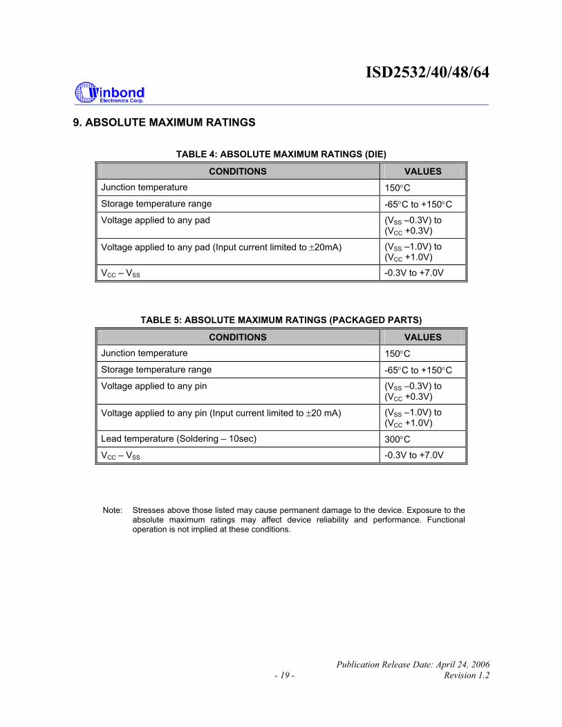
9. ABSOLUTE MAXIMUM RATINGS
TABLE 4: ABSOLUTE MAXIMUM RATINGS (DIE)
CONDITIONS VALUES Junction temperature 150°C
Storage temperature range -65°C to +150°C
Voltage applied to any pad (VSS –0.3V) to (VCC +0.3V)
Voltage applied to any pad (Input current limited to ±20mA) (VSS –1.0V) to (VCC +1.0V)
VCC – VSS -0.3V to +7.0V
TABLE 5: ABSOLUTE MAXIMUM RATINGS (PACKAGED PARTS)
CONDITIONS VALUES Junction temperature 150°C
Storage temperature range -65°C to +150°C
Voltage applied to any pin (VSS –0.3V) to (VCC +0.3V)
Voltage applied to any pin (Input current limited to ±20 mA) (VSS –1.0V) to (VCC +1.0V)
Lead temperature (Soldering – 10sec) 300°C
VCC – VSS -0.3V to +7.0V
Note: Stresses above those listed may cause permanent damage to the device. Exposure to the absolute maximum ratings may affect device reliability and performance. Functional operation is not implied at these conditions.
ISD2532/40/48/64
- 20 -
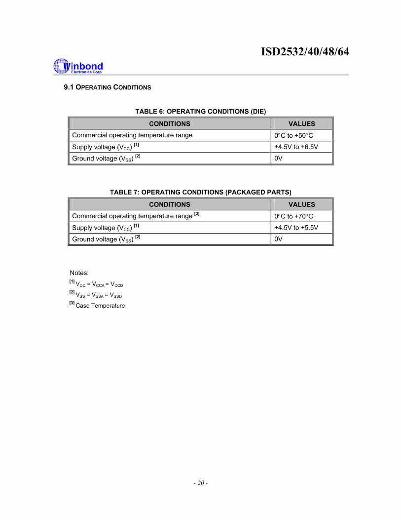
9.1 OPERATING CONDITIONS
TABLE 6: OPERATING CONDITIONS (DIE)
CONDITIONS VALUES Commercial operating temperature range 0°C to +50°C
Supply voltage (VCC) [1] +4.5V to +6.5V
Ground voltage (VSS) [2] 0V
TABLE 7: OPERATING CONDITIONS (PACKAGED PARTS)
CONDITIONS VALUES Commercial operating temperature range [3] 0°C to +70°C
Supply voltage (VCC) [1] +4.5V to +5.5V
Ground voltage (VSS) [2] 0V
Notes: [1] VCC = VCCA = VCCD [2] VSS = VSSA = VSSD
[3] Case Temperature
ISD2532/40/48/64
Publication Release Date: April 24, 2006 - 21 - Revision 1.2
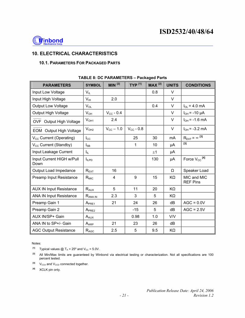
10. ELECTRICAL CHARACTERISTICS
10.1. PARAMETERS FOR PACKAGED PARTS
TABLE 8: DC PARAMETERS – Packaged Parts
PARAMETERS SYMBOL MIN [2] TYP [1] MAX [2] UNITS CONDITIONS Input Low Voltage VIL 0.8 V
Input High Voltage VIH 2.0 V
Output Low Voltage VOL 0.4 V IOL = 4.0 mA
Output High Voltage VOH VCC - 0.4 V IOH = -10 µA
OVF Output High Voltage VOH1 2.4 V IOH = -1.6 mA
EOM Output High Voltage VOH2 VCC – 1.0 VCC - 0.8 V IOH = -3.2 mA
VCC Current (Operating) ICC 25 30 mA REXT = ∞ [3]
VCC Current (Standby) ISB 1 10 µA [3] Input Leakage Current IIL ±1 µA
Input Current HIGH w/Pull Down
IILPD 130 µA Force VCC [4]
Output Load Impedance REXT 16 Ω Speaker Load
Preamp Input Resistance RMIC 4 9 15 KΩ MIC and MIC REF Pins
AUX IN Input Resistance RAUX 5 11 20 KΩ
ANA IN Input Resistance RANA IN 2.3 3 5 KΩ
Preamp Gain 1 APRE1 21 24 26 dB AGC = 0.0V
Preamp Gain 2 APRE2 -15 5 dB AGC = 2.5V
AUX IN/SP+ Gain AAUX 0.98 1.0 V/V
ANA IN to SP+/- Gain AARP 21 23 26 dB
AGC Output Resistance RAGC 2.5 5 9.5 KΩ
Notes: [1] Typical values @ TA = 25º and VCC = 5.0V. [2] All Min/Max limits are guaranteed by Winbond via electrical testing or characterization. Not all specifications are 100
percent tested. [3] VCCA and VCCD connected together. [4] XCLK pin only.

ISD2532/40/48/64
- 22 -
TABLE 9: AC PARAMETERS – Packaged Parts
CHARACTERISTIC SYMBOL MIN[2] TYP[1] MAX[2] UNITS CONDITIONS Sampling Frequency ISD2532 ISD2540 ISD2548 ISD2564
FS 8.0 6.4 5.3 4.0
kHz kHz kHz kHz
[7]
[7]
[7]
[7]
Filter Pass Band ISD2532 ISD2540 ISD2548 ISD2564
FCF 3.4 2.7 2.3 1.7
kHz kHz kHz kHz
3 dB Roll-Off Point [3][8]
3 dB Roll-Off Point [3][8]
3 dB Roll-Off Point [3][8]
3 dB Roll-Off Point [3][8]
Record Duration ISD2532 ISD2540 ISD2548 ISD2564
TREC
32 40 48 64
sec sec sec sec
[7]
[7]
[7]
[7]
Playback Duration ISD2532 ISD2540 ISD2548 ISD2564
TPLAY 32 40 48 64
sec sec sec sec
[7]
[7]
[7]
[7]
CE Pulse Width TCE 100 nsec
Control/Address Setup Time TSET 300 nsec
Control/Address Hold Time THOLD 0 nsec
Power-Up Delay ISD2532 ISD2540 ISD2548 ISD2564
TPUD
25.0 31.0 37.0 50.0
msec msec msec msec
ISD2532/40/48/64
Publication Release Date: April 24, 2006 - 23 - Revision 1.2
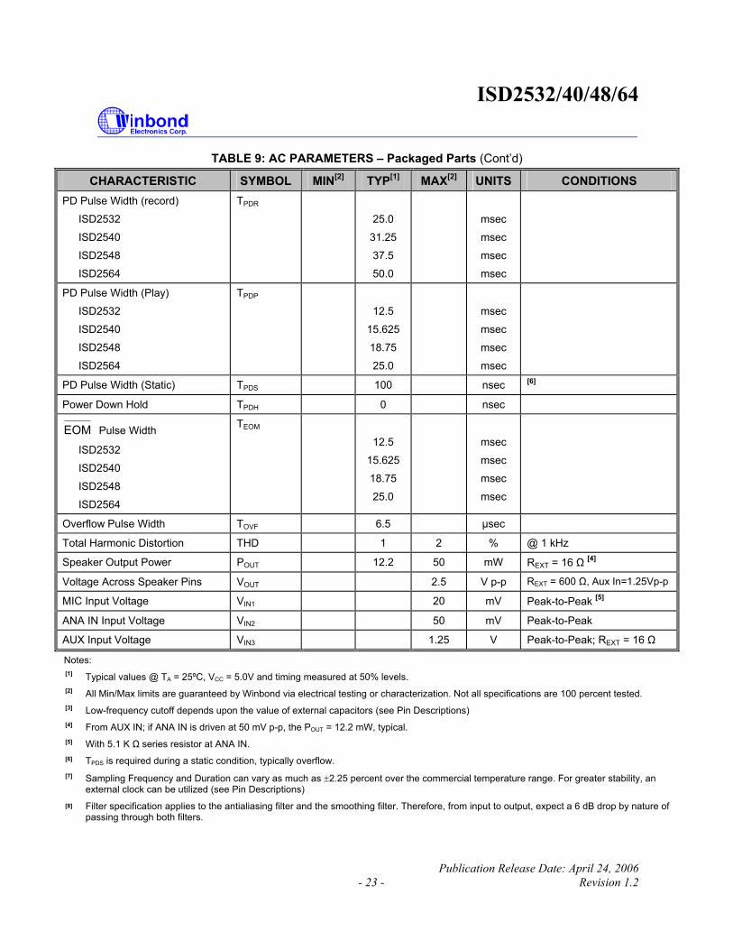
TABLE 9: AC PARAMETERS – Packaged Parts (Cont’d)
CHARACTERISTIC SYMBOL MIN[2] TYP[1] MAX[2] UNITS CONDITIONS PD Pulse Width (record)
ISD2532
ISD2540
ISD2548
ISD2564
TPDR
25.0
31.25
37.5
50.0
msec
msec
msec
msec
PD Pulse Width (Play)
ISD2532
ISD2540
ISD2548
ISD2564
TPDP
12.5
15.625
18.75
25.0
msec
msec
msec
msec
PD Pulse Width (Static) TPDS 100 nsec [6]
Power Down Hold TPDH 0 nsec
EOM Pulse Width
ISD2532
ISD2540
ISD2548
ISD2564
TEOM
12.5
15.625
18.75
25.0
msec
msec
msec
msec
Overflow Pulse Width TOVF 6.5 µsec
Total Harmonic Distortion THD 1 2 % @ 1 kHz
Speaker Output Power POUT 12.2 50 mW REXT = 16 Ω [4]
Voltage Across Speaker Pins VOUT 2.5 V p-p REXT = 600 Ω, Aux In=1.25Vp-p
MIC Input Voltage VIN1 20 mV Peak-to-Peak [5]
ANA IN Input Voltage VIN2 50 mV Peak-to-Peak
AUX Input Voltage VIN3 1.25 V Peak-to-Peak; REXT = 16 Ω
Notes: [1]
[2]
[3]
[4]
[5]
[6]
[7]
[8]
Typical values @ TA = 25ºC, VCC = 5.0V and timing measured at 50% levels.
All Min/Max limits are guaranteed by Winbond via electrical testing or characterization. Not all specifications are 100 percent tested.
Low-frequency cutoff depends upon the value of external capacitors (see Pin Descriptions)
From AUX IN; if ANA IN is driven at 50 mV p-p, the POUT = 12.2 mW, typical.
With 5.1 K Ω series resistor at ANA IN.
TPDS is required during a static condition, typically overflow.
Sampling Frequency and Duration can vary as much as ±2.25 percent over the commercial temperature range. For greater stability, an external clock can be utilized (see Pin Descriptions)
Filter specification applies to the antialiasing filter and the smoothing filter. Therefore, from input to output, expect a 6 dB drop by nature of passing through both filters.

ISD2532/40/48/64
- 24 -
10.1.1. Typical Parameter Variation with Voltage and Temperature - Packaged Parts
-40 25 70 85Temperature (C)
5.5 Volts 4.5 Volts
Perc
ent C
hang
e (%
)
-1.0
-0.8
-0.6
-0.4
-0.2
0
0.2
0.4
Chart 4: Oscillator Stability
-40 25 70 85Temperature (C)
5.5 Volts 4.5 Volts
0
5
10
15
20
25
Ope
ratin
g C
urre
nt (m
A)
Chart 1: Record Mode OperatingCurrent (ICC)
-40 25 70 85Temperature (C)
5.5 Volts 4.5 Volts
Perc
ent D
isto
rtio
n (%
)
0.1
0.2
0.3
0.4
0.5
0.6
0.7
0
Chart 2: Total Harmonic Distortion
-40 25 70 85Temperature (C)
5.5 Volts 4.5 Volts
Stan
dby
Cur
rent
(mA
)0
0.2
0.4
0.6
0.8
1.0
1.2
Chart 3: Standby Current (ISB)

ISD2532/40/48/64
Publication Release Date: April 24, 2006 - 25 - Revision 1.2
10.2. PARAMETERS FOR DIE
TABLE 10: DC PARAMETERS – Die
PARAMETERS SYMBOL MIN[2] TYP[1] MAX[2] UNITS CONDITIONS Input Low Voltage VIL 0.8 V
Input High Voltage VIH 2.0 V
Output Low Voltage VOL 0.4 V IOL = 4.0 mA
Output High Voltage VOH VCC - 0.4 V IOH = -10 µA
OVF Output High Voltage VOH1 2.4 V IOH = -1.6 mA
EOM Output High Voltage VOH2 VCC – 1.0 VCC - 0.8
V IOH = -3.2 mA
VCC Current (Operating) ICC 25 30 mA REXT = ∞ [3]
VCC Current (Standby) ISB 1 10 µA [2] Input Leakage Current IIL ±1 µA
Input Current HIGH w/Pull Down
IILPD 130 µA Force VCC [4]
Output Load Impedance REXT 16 Ω Speaker Load
Preamp IN Input Resistance
RMIC 4 9 15 KΩ MIC and MIC REF Pads
AUX IN Input Resistance RAUX 5 11 20 KΩ
ANA IN Input Resistance RANA IN 2.3 3 5 KΩ
Preamp Gain 1 APRE1 21 24 26 dB AGC = 0.0V
Preamp Gain 2 APRE2 -15 5 dB AGC = 2.5V
AUX IN/SP+ Gain AAUX 0.98 1.0 V/V
ANA IN to SP+/- Gain AARP 21 23 26 dB
AGC Output Resistance RAGC 2.5 5 9.5 KΩ
Notes: [1] Typical values @ TA = 25°C and VCC = 5.0V. [2] All Min/Max limits are guaranteed by Winbond via electrical testing or characterization. Not all specifications are 100
percent tested. [3] VCCA and VCCD connected together. [4] XCLK pad only.

ISD2532/40/48/64
- 26 -
TABLE 11: AC PARAMETERS – Die
CHARACTERISTIC SYMBOL MIN[2] TYP[1] MAX[2] UNITS CONDITIONS Sampling Frequency ISD2532 ISD2540 ISD2548 ISD2564
FS 8.0 6.4 5.3 4.0
kHz kHz kHz kHz
[7]
[7]
[7]
[7]
Filter Pass Band ISD2532 ISD2540 ISD2548 ISD2564
FCF 3.4 2.7 2.3 1.7
kHz kHz kHz kHz
3 dB Roll-Off Point [3][8]
3 dB Roll-Off Point [3][8]
3 dB Roll-Off Point [3][8]
3 dB Roll-Off Point [3][8]
Record Duration ISD2532 ISD2540 ISD2548 ISD2564
TREC
32 40 48 64
sec sec sec sec
[7]
[7]
[7]
[7]
Playback Duration
ISD2532 ISD2540 ISD2548 ISD2564
TPLAY
32 40 48 64
sec sec sec sec
[7]
[7]
[7]
[7]
CE Pulse Width TCE 100 nsec
Control/Address Setup Time TSET 300 nsec
Control/Address Hold Time THOLD 0 nsec
Power-Up Delay ISD2532 ISD2540 ISD2548 ISD2564
TPUD
25.0 31.3 37.5 50.0
msec msec msec msec

ISD2532/40/48/64
Publication Release Date: April 24, 2006 - 27 - Revision 1.2
TABLE 11: AC PARAMETERS – Die (Cont’d)
CHARACTERISTIC SYMBOL MIN[2] TYP[1] MAX[2] UNITS CONDITIONS PD Pulse Width (Record)
ISD2532
ISD2540
ISD2548
ISD2564
TPDR
25.0
31.25
37.5
50.0
msec
msec
msec
msec
PD Pulse Width (Play)
ISD2532
ISD2540
ISD2548
ISD2564
TPDP
12.5
15.625
18.75
25.0
msec
msec
msec
msec
PD Pulse Width (Static) TPDS 100 nsec [6]
Power Down Hold TPDH 0 nsec
EOM Pulse Width
ISD2532
ISD2540
ISD2548
ISD2564
TEOM
12.5
15.625
18.75
25.0
msec
msec
msec
msec
Overflow Pulse Width TOVF 6.5 µsec
Total Harmonic Distortion THD 1 2 % @ 1 kHz
Speaker Output Power POUT 12.2 50 mW REXT = 16 Ω [4]
Voltage Across Speaker Pins VOUT 2.5 V p-p REXT=600 Ω, Aux In=1.25Vp-p
MIC Input Voltage VIN1 20 mV Peak-to-Peak [5]
ANA IN Input Voltage VIN2 50 mV Peak-to-Peak
AUX Input Voltage VIN3 1.25 V Peak-to-Peak; REXT = 16 Ω
Notes: [1] Typical values @ TA = 25°C, VCC = 5.0V and timing measured at 50% levels. [2] All Min/Max limits are guaranteed by Winbond via electrical testing or characterization. Not all specifications are 100 percent tested. [3] Low-frequency cutoff depends upon the value of external capacitors (see Pin Descriptions) [4] From AUX IN; if ANA IN is driven at 50 mV p-p, the POUT = 12.2 mW, typical. [5] With 5.1 K Ω series resistor at ANA IN. [6] TPDS is required during a static condition, typically overflow. [7] Sampling Frequency and playback Duration can vary as much as ±2.25 percent over the commercial temperature range. For greater stability,
an external clock can be utilized (see Pin Descriptions) [8] Filter specification applies to the antialiasing filter and the smoothing filter. Therefore, from input to output, expect a 6 dB drop by nature of
passing through both filters.
ISD2532/40/48/64
- 28 -
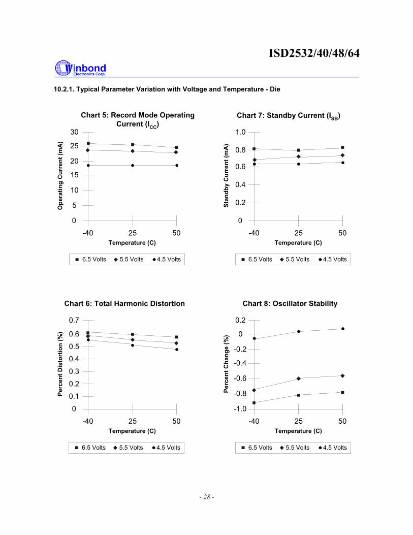
10.2.1. Typical Parameter Variation with Voltage and Temperature - Die
-40 25 50Temperature (C)
Perc
ent C
hang
e (%
)
-1.0
-0.8
-0.6
-0.4
-0.2
0
0.2
Chart 8: Oscillator Stability
6.5 Volts 5.5 Volts 4.5 Volts
-40 25 50Temperature (C)
Perc
ent D
isto
rtio
n (%
)
0.1
0.2
0.3
0.4
0.5
0.6
0.7
0
Chart 6: Total Harmonic Distortion
6.5 Volts 5.5 Volts 4.5 Volts
5
10
15
20
25
30
-40 25 50Temperature (C)
0
Ope
ratin
g C
urre
nt (m
A)
Chart 5: Record Mode OperatingCurrent (ICC)
6.5 Volts 5.5 Volts 4.5 Volts
-40 25 50Temperature (C)
Stan
dby
Cur
rent
(mA
)0
Chart 7: Standby Current (ISB)
0.2
0.4
0.6
0.8
1.0
6.5 Volts 5.5 Volts 4.5 Volts

ISD2532/40/48/64
Publication Release Date: April 24, 2006 - 29 - Revision 1.2
10.3. PARAMETERS FOR PUSH-BUTTON MODE
TABLE 12: PARAMETERS FOR PUSH-BUTTON MODE
PARAMETERS SYMBOL MIN[2] TYP[1] MAX[2] UNITS CONDITIONS
CE Pulse Width (Start/Pause)
TCE 300 nsec
Control/Address Setup Time TSET 300 nsec
Power-Up Delay ISD2532 ISD2540 ISD2548 ISD2564
TPUD 25.0 31.25 37.25 50.0
msec msec msec msec
PD Pulse Width (Stop/Restart) TPD 300 nsec
CE to EOM HIGH TRUN 25 400 nsec
CE to EOM LOW TPAUSE 50 400 nsec
CE HIGH Debounce
ISD2532 ISD2540 ISD2548 ISD2564
TDB 70 85 105 135
105 135 160 215
msec msec msec msec
Notes:
[1] Typical values @ TA = 25°C, VCC = 5.0V and timing measured at 50% levels. [2] All Min/Max limits are guaranteed by Winbond via electrical testing or characterization. Not all specifications are 100
percent tested.

ISD2532/40/48/64
- 30 -
11. TYPICAL APPLICATION CIRCUIT
VCC
VCCD
VCCA
VSSD
VSSA
SP+SP-
MIC REFMIC
AGC
AUX INANA IN
ANA OUT
A0A1A2A3A4A5A6
A7A8
CEPDP/ROEMOVFXCLK
100 KΩR4
VSS
CHIP ENABLE
POWER DOWN
PLAYBACK/RECORD
C30.1 Fµ5.1 KΩ
R6
C24.7 Fµ470 KΩ
R2
C50.1 Fµ
10 KΩR5
ELECTRETMICROPHONE
SPEAKER16Ω
VCC
C60.1 Fµ
C70.1 Fµ C8
22 Fµ
VCCC1
0.1 Fµ
C4220 Fµ
1 KΩR1
10 KΩR3
ISD2532/40/48/64
1234567
910
232427252226 19
1718
21
20111514
13
12
1628
(Note)
FIGURE 5: DESIGN SCHEMATIC Note: If desired, pin 18 (PDIP package) may be left unconnected (microphone preamplifier noise will be higher). In this case, pin 18 must not be tied to any other signal or voltage. Additional design example schematics are provided below.
ISD2532/40/48/64
Publication Release Date: April 24, 2006 - 31 - Revision 1.2
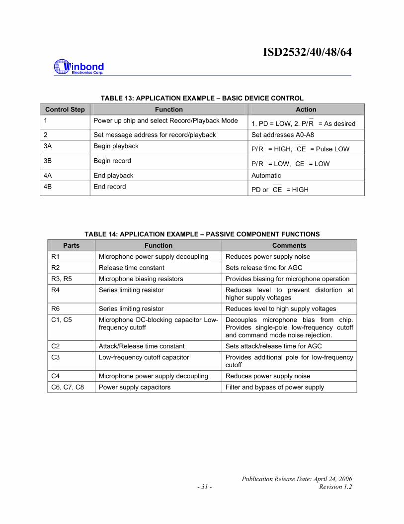
TABLE 13: APPLICATION EXAMPLE – BASIC DEVICE CONTROL
Control Step Function Action 1 Power up chip and select Record/Playback Mode 1. PD = LOW, 2. P/R = As desired
2 Set message address for record/playback Set addresses A0-A8
3A Begin playback P/R = HIGH, CE = Pulse LOW
3B Begin record P/R = LOW, CE = LOW
4A End playback Automatic
4B End record PD or CE = HIGH
TABLE 14: APPLICATION EXAMPLE – PASSIVE COMPONENT FUNCTIONS Parts Function Comments
R1 Microphone power supply decoupling Reduces power supply noise
R2 Release time constant Sets release time for AGC
R3, R5 Microphone biasing resistors Provides biasing for microphone operation
R4 Series limiting resistor Reduces level to prevent distortion at higher supply voltages
R6 Series limiting resistor Reduces level to high supply voltages
C1, C5 Microphone DC-blocking capacitor Low-frequency cutoff
Decouples microphone bias from chip. Provides single-pole low-frequency cutoff and command mode noise rejection.
C2 Attack/Release time constant Sets attack/release time for AGC
C3 Low-frequency cutoff capacitor Provides additional pole for low-frequency cutoff
C4 Microphone power supply decoupling Reduces power supply noise
C6, C7, C8 Power supply capacitors Filter and bypass of power supply

ISD2532/40/48/64
- 32 -
S2
VCC
U1
PB0PB1
PA0PA1
OSC1OSC2
RESETIRQ PA2
PA3PA4PA5PA6PA7
VDD
VSS
S1
26
U2
VCCD
VCCA
VSSD
VSSA
SP+SP-
MIC REFMIC
AGC
AUX INANA IN
ANA OUT
A0A1A2A3A4A5A6
A7A8
CEPDP/ROEMOVFXCLK
ISD2532/40/48/64
1234567
910
2324272522
19
1718
21
20111514
13
12
1628
S3
RECORD PLAY MSG#MC68HC705K1A
RUND1
R1TBD
FIGURE 6: ISD2532/40/48/64 APPLICATION EXAMPLE – MICROCONTROLLER/ISD2500
INTERFACE
In this simplified block diagram of a microcontroller application, the Push-Button Mode and message cueing are used. The microcontroller is a 16-pin version with enough port pins for buttons, an LED, and the ISD2500 series device. The software can be written to use three buttons: one each for play and record, and one for message selection. Because the microcontroller is interpreting the buttons and commanding the ISD2500 device, software can be written for any function desired in a particular application. Note: Winbond does not recommend connecting address lines directly to a microprocessor bus. Address lines should be externally latched.
ISD2532/40/48/64
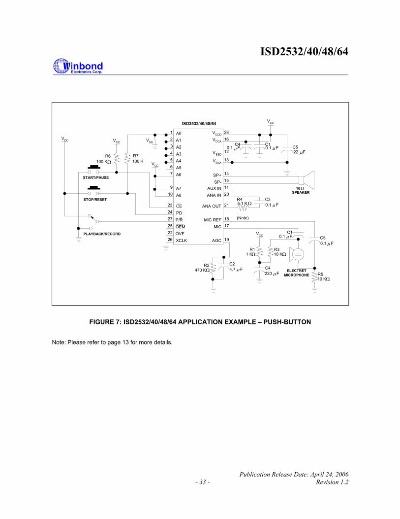
Publication Release Date: April 24, 2006 - 33 - Revision 1.2
ISD2532/40/48/64
VCCD
VCCA
VSSD
VSSA
SP+SP-
MIC REFMIC
AGC
AUX INANA IN
ANA OUT
A0A1A2A3A4A5A6
A7A8
CEPDP/ROEMOVFXCLK
C24.7 Fµ470 KΩ
R2
C50.1 Fµ
10 KΩR5
ELECTRETMICROPHONE
SPEAKER16Ω
VCCC1
0.1 Fµ
C4220 Fµ
1 KΩR1
10 KΩR3
C30.1 Fµ5.1 KΩ
R4
VCC
C40.1 Fµ
C10.1 Fµ C5
22 Fµ
19
1718
21
20111514
13
12
1628
100 KR7
VSS
START/PAUSE
STOP/RESET
PLAYBACK/RECORD
1234567
910
232427252226
VCC
VCCVCC
(Note)
R6100 KΩ
FIGURE 7: ISD2532/40/48/64 APPLICATION EXAMPLE – PUSH-BUTTON
Note: Please refer to page 13 for more details.
ISD2532/40/48/64
- 34 -
TABLE 15: APPLICATION EXAMPLE – PUSH-BUTTON CONTROL Control Step Function Action 1 Select Record/Playback Mode P/R = As desired
2A Begin playback P/R = HIGH, CE = Pulse LOW
2B Begin record P/R = LOW, CE = Pulse LOW
3 Pause record or playback CE = Pulsed LOW
4A End playback Automatic at EOM marker or PD = Pulsed HIGH
4B End record PD = Pulsed HIGH
TABLE 16: APPLICATION EXAMPLE – PASSIVE COMPONENT FUNCTIONS Parts Function Comments
R2 Release time constant Sets release time for AGC
R4 Series limiting resistor Reduces level to prevent distortion at higher supply voltages
R6, R7 Pull-up and pull-down resistors Defines static state of inputs
C1, C4, C5 Power supply capacitors Filters and bypass of power supply
C2 Attack/Release time constant Sets attack/release time for AGC
C3 Low-frequency cutoff capacitor Provides additional pole for low-frequency cutoff
ISD2532/40/48/64
Publication Release Date: April 24, 2006 - 35 - Revision 1.2
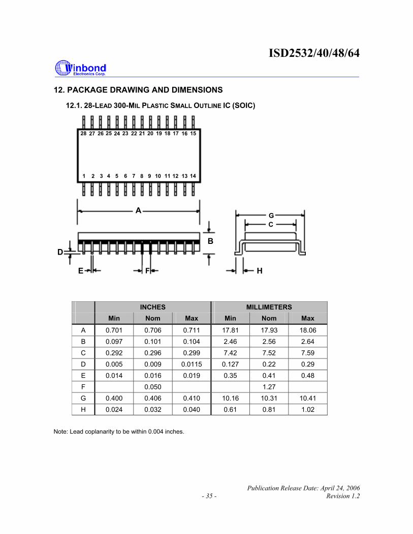
12. PACKAGE DRAWING AND DIMENSIONS
12.1. 28-LEAD 300-MIL PLASTIC SMALL OUTLINE IC (SOIC)
28 27 26 25 24 23 22 21 20 19 18 17 16 15
1 2 3 4 5 6 7 8 9 10 11 12 13 14
A
D
E F
B
GC
H
INCHES MILLIMETERS Min Nom Max Min Nom Max
A 0.701 0.706 0.711 17.81 17.93 18.06
B 0.097 0.101 0.104 2.46 2.56 2.64
C 0.292 0.296 0.299 7.42 7.52 7.59
D 0.005 0.009 0.0115 0.127 0.22 0.29
E 0.014 0.016 0.019 0.35 0.41 0.48
F 0.050 1.27
G 0.400 0.406 0.410 10.16 10.31 10.41
H 0.024 0.032 0.040 0.61 0.81 1.02
Note: Lead coplanarity to be within 0.004 inches.
ISD2532/40/48/64
- 36 -
12.2. 28-LEAD 600-MIL PLASTIC DUAL INLINE PACKAGE (PDIP)
INCHES MILLIMETERS Min Nom Max Min Nom Max
A 1.445 1.450 1.455 36.70 36.83 36.96
B1 0.150 3.81
B2 0.065 0.070 0.075 1.65 1.78 1.91
C1 0.600 0.625 15.24 15.88
C2 0.530 0.540 0.550 13.46 13.72 13.97
D 0.19 4.83
D1 0.015 0.38
E 0.125 0.135 3.18 3.43
F 0.015 0.018 0.022 0.38 0.46 0.56
G 0.055 0.060 0.065 1.40 1.52 1.62
H 0.100 2.54
J 0.008 0.010 0.012 0.20 0.25 0.30
S 0.070 0.075 0.080 1.78 1.91 2.03
q 0° 15° 0° 15°

ISD2532/40/48/64
Publication Release Date: April 24, 2006 - 37 - Revision 1.2
12.3. DIE BONDING PHYSICAL LAYOUT [1]
ISD2532/40/48/64 o Die Dimensions
X: 149.6 + 1 mils Y: 206.3 + 1 mils
o Die Thickness [2]
11.5 + .4 mils
o Pad Opening 111 x 111 microns
(4.4 x 4.4 mils)
Notes:
[1] The backside of die is internally connected to VSS. It MUST NOT be connected to any other potential or damage may occur.
[2] Die thickness is subject to change, please contact Winbond factory for status and availability.
≈≈
ISD2532/40/48/64
A3A2
A1A0
VCCD
P/RXCLK
EOM PD
CE
OVF
A4
A5
A6
ANA OUT
ANA IN
AGC
MIC REF
MICSP-
SP+VSSD
AUX IN
A8
A7
NC
VSSA
VCCA

ISD2532/40/48/64
- 38 -
ISD2532/40/48/64 PRODUCT PAD DESIGNATIONS (with respect to die center)
Pad Pad Name X Axis (µm) Y Axis (µm)
OVF Overflow Output 1675.95 1779.38
CE Chip Enable Input 1728.08 2114.25
PD Power Down Input 1731.83 2383.88
EOM End of Message 1342.20 2411.63
XCLK No Connect (optional) 987.83 2450.63
P/R Playback/Record 808.58 2453.25
VCCD VCC Digital Power Supply 546.08 2449.13
A0 Address 0 -896.55 2425.13
A1 Address 1 -1114.05 2425.13
A2 Address 2 -1329.68 2425.13
A3 Address 3 -1542.68 2425.13
A4 Address 4 -1639.05 2178.75
A5 Address 5 -1696.80 1960.88
A6 Address 6 -1696.80 1731.38
NC NC -1729.80 -1875.75
A7 Address 7 -1729.80 -2061.00
A8 Address 8 -1729.80 -2343.38
AUX IN Auxiliary Input -1408.80 -2408.25
VSSD VSS Digital Power Supply -1111.43 -2388.75
VSSA VSS Analog Power Supply -406.43 -2431.13
SP+ Speaker Output + -46.05 -2360.25
SP- Speaker Output - 388.20 -2360.25
VCCA VCC Analog Power Supply 747.83 -2403.00
MIC Microphone Input 1102.58 -2438.63
MIC REF Microphone Reference 1296.08 -2438.63
AGC Automatic Gain Control 1667.70 -2422.88
ANA IN Analog Input 1729.95 -1946.63
ANA OUT Analog Output 1702.20 -1703.63

ISD2532/40/48/64
Publication Release Date: April 24, 2006 - 39 - Revision 1.2
13. ORDERING INFORMATION Product Number Descriptor Key
When ordering ISD2532/40/48/64 products, please refer to the following part numbers. Also, please contact the local Winbond Sales Representative or Distributor for availability on the lead-free parts.
Type Package 32 Seconds 40 Seconds 48 Seconds 64 Seconds
Die Die ISD2532X ISD2540X ISD2548X ISD2564X
PDIP ISD2532P ISD2540P ISD2548P ISD2564P Leaded SOIC ISD2532S ISD2540S ISD2548S
PDIP ISD2532PY ISD2540PY ISD2548PY ISD2564PY Lead-Free SOIC ISD2532SY ISD2540SY ISD2548SY
For the latest product information, access Winbond’s worldwide website at http://www.winbond-usa.com
Package Type:
P = 28-Lead 600mil Plastic Dual Inline Package (PDIP) S = 28-Lead 300mil Small Outline Integrated Circuit (SOIC)
X = Die
Special Temperature Field: Blank = Commercial Packaged (0˚C to +70˚C)
or Commercial Die (0˚C to +50˚C)
ISD2 5 _
ISD2500 Series
Duration: 32 = 32 seconds
40 = 40 seconds
48 = 48 seconds
64 = 64 seconds
Package Option: Y = Lead-free
Blank = Leaded

ISD2532/40/48/64
- 40 -
14. VERSION HISTORY VERSION DATE DESCRIPTION
0 Apr. 1998 Preliminary Specifications.
1.0 Jun. 2003 Reformat the document. Update TSOP description in pin configuration section. Revise Table 1: Product Summary. Update TSOP and SOIC package option. Remove industrial temperature option.
1.1 Apr 2005 Revise the disclaim section.
1.2 Apr 2006 Add lead-free option. Remove TSOP information.

ISD2532/40/48/64
Publication Release Date: April 24, 2006 - 41 - Revision 1.2
Headquarters Winbond Electronics Corporation America Winbond Electronics (Shanghai) Ltd.
No. 4, Creation Rd. III 2727 North First Street, San Jose, 27F, 299 Yan An W. Rd. Shanghai, Science-Based Industrial Park, CA 95134, U.S.A. 200336 China Hsinchu, Taiwan TEL: 1-408-9436666 TEL: 86-21-62365999 TEL: 886-3-5770066 FAX: 1-408-5441797 FAX: 86-21-62356998 FAX: 886-3-5665577 http://www.winbond-usa.com/ http://www.winbond.com.tw/
Taipei Office Winbond Electronics Corporation Japan Winbond Electronics (H.K.) Ltd. 9F, No. 480, Pueiguang Rd. 7F Daini-ueno BLDG. 3-7-18 Unit 9-15, 22F, Millennium City, Neihu District Shinyokohama Kohokuku, No. 378 Kwun Tong Rd., Taipei, 114 Taiwan Yokohama, 222-0033 Kowloon, Hong Kong TEL: 886-2-81777168 TEL: 81-45-4781881 TEL: 852-27513100 FAX: 886-2-87153579 FAX: 81-45-4781800 FAX: 852-27552064
Please note that all data and specifications are subject to change without notice. All the trademarks of products and companies mentioned in this datasheet belong to their respective owners.
Winbond products are not designed, intended, authorized or warranted for use as components in systems or equipment intended for surgical implantation, atomic energy control instruments, airplane or spaceship instruments, transportation instruments, traffic signal instruments, combustion control instruments, or for other applications intended to support or sustain life. Furthermore, Winbond products are not intended for applications wherein failure of Winbond products could result or lead to a situation wherein personal injury, death or severe property or environmental damage could occur.
Winbond customers using or selling these products for use in such applications do so at their own risk and agree to fully indemnify Winbond for any damages resulting from such improper use or sales.
The contents of this document are provided only as a guide for the applications of Winbond products. Winbond makes no representation or warranties with respect to the accuracy or completeness of the contents of this publication and reserves the right to discontinue or make changes to specifications and product descriptions at any time without notice. No license, whether express or implied, to any intellectual property or other right of Winbond or others is granted by this publication. Except as set forth in Winbond's Standard Terms and Conditions of Sale, Winbond assumes no liability whatsoever and disclaims any express or implied warranty of merchantability, fitness for a particular purpose or infringement of any Intellectual property.
The contents of this document are provided “AS IS”, and Winbond assumes no liability whatsoever and disclaims any express or implied warranty of merchantability, fitness for a particular purpose or infringement of any Intellectual property. In no event, shall Winbond be liable for any damages whatsoever (including, without limitation, damages for loss of profits, business interruption, loss of information) arising out of the use of or inability to use the contents of this documents, even if Winbond has been advised of the possibility of such damages.
Application examples and alternative uses of any integrated circuit contained in this publication are for illustration only and Winbond makes no representation or warranty that such applications shall be suitable for the use specified.
The 100-year retention and 100K record cycle projections are based upon accelerated reliability tests, as published in the Winbond Reliability Report, and are neither warranted nor guaranteed by Winbond. This product incorporates SuperFlash®.
Information contained in this ISD® ChipCorder® datasheet supersedes all data for the ISD ChipCorder products published by ISD® prior to August, 1998.
This datasheet and any future addendum to this datasheet is(are) the complete and controlling ISD® ChipCorder® product specifications. In the event any inconsistencies exist between the information in this and other product documentation, or in the event that other product documentation contains information in addition to the information in this, the information contained herein supersedes and governs such other information in its entirety. This datasheet is subject to change without notice.
Copyright© 2005, Winbond Electronics Corporation. All rights reserved. ChipCorder® and ISD® are trademarks of Winbond Electronics Corporation. SuperFlash® is the trademark of Silicon Storage Technology, Inc. All other trademarks are properties of their respective owners.