IS32LT3120 - ISSI IS32LT3120 is targeted at the automotive market with end applications to include...
16
IS32LT3120 Integrated Silicon Solution, Inc. – www.issi.com Rev.A, 12/10/2015 1 DUAL CHANNEL, LINEAR LED DRIVER WITH FADE IN/FADE OUT December 2015 GENERAL DESCRIPTION The IS32LT3120 is a linear programmable current regulator consisting of 2 output channels capable of up to 200mA each. Each channel features an ON/OFF input pin to toggle the channel between the OFF condition and the source condition. A single external resistor programs the current level for both of the channels, while a separate, single resistor programs the fade in and fade out rate for both channels. The device integrates a 63 steps fade in and fade out algorithm (Gamma correction) which causes the output LED current to gradually ramp up to the full source value after the channel’s control pin is pulsed. The same controller causes the LED current to gradually ramp down to zero if the channel’s input control pin is pulsed while the output channel is on. The LED current output can be controlled by a momentary contact switch or logic level signal. The IS32LT3120 is targeted at the automotive market with end applications to include map and dome lighting as well as exterior accent lighting. For 12V automotive applications the low dropout driver can support 1 to 3 LEDs per channel. It is offered in a small thermally enhanced SOP-8-EP package. FEATURES Dual output channels can source up to 200mA each Independent on/off control for each channel -Inputs are debounced Programmable current via a single external resistor Programmable fade in, fade out via external resistor - Pull down resistor value sets fade speed - Gamma corrected fade in/out algorithm Fault Protection: - OUTx pin shorted to GND - ISET pin short to GND - Over temperature SOP-8-EP package Automotive Grade - AEC-Q100 Operating temperature range from -40°C ~ +125°C APPLICATIONS Automotive Interior: - Map light - Dome lighting - Puddle lamp in doors - Glove box - Vanity mirror TYPICAL APPLICATION CIRCUIT Figure 1 Typical Application Circuit Note: The switches on ENx pin should be momentary touch type.
Transcript of IS32LT3120 - ISSI IS32LT3120 is targeted at the automotive market with end applications to include...

IS32LT3120
Integrated Silicon Solution, Inc. – www.issi.com Rev.A, 12/10/2015
1
DUAL CHANNEL, LINEAR LED DRIVER WITH FADE IN/FADE OUT
December 2015 GENERAL DESCRIPTION
The IS32LT3120 is a linear programmable current regulator consisting of 2 output channels capable of up to 200mA each. Each channel features an ON/OFF input pin to toggle the channel between the OFF condition and the source condition.
A single external resistor programs the current level for both of the channels, while a separate, single resistor programs the fade in and fade out rate for both channels.
The device integrates a 63 steps fade in and fade out algorithm (Gamma correction) which causes the output LED current to gradually ramp up to the full source value after the channel’s control pin is pulsed. The same controller causes the LED current to gradually ramp down to zero if the channel’s input control pin is pulsed while the output channel is on. The LED current output can be controlled by a momentary contact switch or logic level signal.
The IS32LT3120 is targeted at the automotive market with end applications to include map and dome lighting as well as exterior accent lighting. For 12V automotive applications the low dropout driver can support 1 to 3 LEDs per channel. It is offered in a small thermally enhanced SOP-8-EP package.
FEATURES
Dual output channels can source up to 200mA each
Independent on/off control for each channel -Inputs are debounced
Programmable current via a single external resistor
Programmable fade in, fade out via external resistor - Pull down resistor value sets fade speed - Gamma corrected fade in/out algorithm
Fault Protection: - OUTx pin shorted to GND - ISET pin short to GND - Over temperature
SOP-8-EP package Automotive Grade - AEC-Q100 Operating temperature range from -40°C ~ +125°C
APPLICATIONS
Automotive Interior: - Map light - Dome lighting - Puddle lamp in doors - Glove box - Vanity mirror
TYPICAL APPLICATION CIRCUIT
Figure 1 Typical Application Circuit
Note: The switches on ENx pin should be momentary touch type.

IS32LT3120
Integrated Silicon Solution, Inc. – www.issi.com Rev.A, 12/01/2015
2
PIN CONFIGURATION
Package Pin Configuration (Top view)
SOP-8-EP
PIN DESCRIPTION
No. Pin Description
1 TSET
Timing control for the fade in and fade out feature. Connect a resistor between this pin and GND to set the fade in and fade out time. Connect this pin directly to ground to disable the fade function for instant on/off.
2 ISET Output current setting for both channel 1 and channel 2. Connect a resistor between this pin and GND to set the maximum output current.
3 GND Ground pin for the device.
4 OUT1 Output current source channel 1.
5 OUT2 Output current source channel 2.
6 VCC Power supply input pin.
7 EN2
Internally debounced input pin for control of channel 2. Momentary contact will toggle the state of the corresponding OUT2 LED. Fade in or out function can be interrupted by EN2 pin state change after debounce period.
8 EN1
Internally debounced input pin for control of channel 1. Momentary contact will toggle the state of the corresponding OUT1 LED. Fade in or out function can be interrupted by EN1 pin state change after debounce period.
Thermal Pad Connect to GND.

IS32LT3120
Integrated Silicon Solution, Inc. – www.issi.com Rev.A, 12/10/2015
3
ORDERING INFORMATION Automotive Range: -40°C to +125°C
Order Part No. Package QTY/Reel
IS32LT3120-GRLA3-TR SOP-8-EP, Lead-free 2500
Copyright © 2015 Integrated Silicon Solution, Inc. All rights reserved. ISSI reserves the right to make changes to this specification and its products at any time without notice. ISSI assumes no liability arising out of the application or use of any information, products or services described herein. Customers are advised to obtain the latest version of this device specification before relying on any published information and before placing orders for products. Integrated Silicon Solution, Inc. does not recommend the use of any of its products in life support applications where the failure or malfunction of the product can reasonably be expected to cause failure of the life support system or to significantly affect its safety or effectiveness. Products are not authorized for use in such applications unless Integrated Silicon Solution, Inc. receives written assurance to its satisfaction, that: a.) the risk of injury or damage has been minimized; b.) the user assume all such risks; and c.) potential liability of Integrated Silicon Solution, Inc is adequately protected under the circumstances

IS32LT3120
Integrated Silicon Solution, Inc. – www.issi.com Rev.A, 12/01/2015
4
ABSOLUTE MAXIMUM RATINGS VCC, OUT1, OUT2 -0.3V ~ +50V EN1, EN2, ISET, TSET -0.3V ~ +7.0V Ambient operating temperature, TA -40°C ~ +125°C Maximum continuous junction temperature, TJ(MAX) 150°C Storage temperature range, TSTG -55°C ~ +150°C Maximum power dissipation, PDMAX 1.96W ESD (HBM) ESD (CDM)
±2kV ±750V
Note: Stresses beyond those listed under “Absolute Maximum Ratings” may cause permanent damage to the device. These are stress ratings only and functional operation of the device at these or any other condition beyond those indicated in the operational sections of the specifications is not implied. Exposure to absolute maximum rating conditions for extended periods may affect device reliability. THERMAL CHARACTERISTICS
Characteristic Test Conditions Value
Package Thermal Resistance (Junction to Ambient), RθJA
On 4-layer PCB based on JEDEC standard at 1W, TA=25°C
50.98°C/W
Package Thermal Resistance (Junction to Pad), RθJP
2.24°C/W
ELECTRICAL CHARACTERISTICS TJ = -40°C ~ +125°C, VCC=12V, the detail refer to each condition description. Typical values are at TJ = 25°C.
Symbol Parameter Condition Min. Typ. Max. Unit
VCC Supply voltage range 6 45 V
VDO Minimum dropout voltage VCC – VOUTx, IOUTx= -200mA (Note1) 900 mV
VCC – VOUTx, IOUTx= -100mA (Note1) 700 mV
ICC Quiescent supply current
OUT1 and OUT2 is shutdown 0.1 1 mA
ISET=20kΩ, enable. OUTx connected to VCC
3.6 mA
tON Startup time VCC> 6V to IOUTx<-5mA (Note 4) 400 μs
IOUT_LIM Output limit current VCC – VOUTx =1V, OUTx sourcing current, VISET = 0V
-310 -240 -205 mA
IOUT Output current (Note 2,3) ISET = 20kΩ, VCC – VOUTx =1V -105 -100 -95 mA
EIOUT Absolute current accuracy (Note 2,3)
-50mA≤IOUTx<-20mA, VCC – VOUTx =1V, -40°C<TJ<+125°C
-8 8 %
-200mA<IOUTx<-50mA, VCC – VOUTx =1V, -40°C<TJ<+125°C
-6 6 %
EIOUTM Channel to channel current matching (Note 2,3)
IOUTx = -100mA, VCC – VOUTx =1V, TJ = 25°C
2 %
IOUTx = -100mA, VCC – VOUTx =1V, -40°C < TJ < +125°C
4 %
gLINE Output current line regulation IOUTx = -50mA, 6V<VCC<18V, VOUT = VCC -2V (Note 4)
-0.2 0.2 mA/V
gLOAD Output current load regulation
2.5V < VOUTx < VCC-2.0V, IOUTx = -50mA (Note 4)
-0.2 0.2 mA/V
tSL Current slew time Current rise/fall between 0%~100% VTSET = 0V
45 70 100 μs

IS32LT3120
Integrated Silicon Solution, Inc. – www.issi.com Rev.A, 12/10/2015
5
ELECTRICAL CHARACTERISTICS (CONTINUE) TJ = -40°C ~ +125°C, VCC=12V, the detail refer to each condition description. Typical values are at TJ = 25°C.
Symbol Parameter Condition Min. Typ. Max. Unit
Logic Input TSET
VTSET Voltage reference 1 V
TACC Fade timing accuracy *Neglecting the RTSET Tolerance* RTSET=100kΩ, TJ = 25°C
-5 5 %
Logic Input ENx
VIL Input low voltage 0.8 V
VIH Input high voltage 2 V
VIN_HY Input hysteresis (Note 4) 150 350 mV
RPU Pull-up resistor (Note 4) 50 kΩ
IPU Pull-up current 75 μA
tSW ENx input debounce time ENx pin must not change state within this time to be interpreted as a switch press or release
25 37 50 ms
Protection
VSCD Short detect voltage Measured at OUTx 1.2 1.8 V
VSC_HY Short detect voltage hysteresis VSCR - VSCD (Note 4) 220 mV
tFD Fault detect persistence time (Note 4) 5 ms
TRO Thermal roll off threshold (Note 4) 130 °C
TSD Thermal shutdown threshold Temperature increasing (Note 4) 155 °C
THY Over temperature hysteresis Recovery = TSHT - TJ_HY (Note 4) 20 °C
Note 1: IOUTX output current in case of VCC-VOUTX=VDO called IOUT_VDO. IOUTX output current in case of VCC-VOUTX=1V called IOUT_VDO1V, VDO accuracy is computed as |IOUT_VDO-IOUT_VDO1V|/IOUT_VDO1V<5%.
Note 2: Output current accuracy is computed as 100×[1 - 2×IOUTx/(IOUT1+IOUT2)]. Output current channel to channel match is computed as 100 × [Max ( |IOUTx– IOUT(AV)| ) / IOUT(AV)] , where IOUT(AV) is the average current of all active outputs.
Note 3: Output current accuracy is not intended to be guaranteed at output voltages less than 1.8V.
Note 4: Guaranteed by design.
IS32LT3120
Integrated Silicon Solution, Inc. – www.issi.com Rev.A, 12/01/2015
6
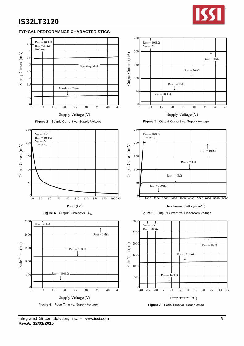
TYPICAL PERFORMANCE CHARACTERISTICS
Sup
ply
Cur
rent
(m
A)
Supply Voltage (V)
5 10 15 20 25 30 35 40 450
0.5
1
1.5
2
2.5
3
3.5
4
4.5
5
RTSET = 100kΩRISET = 20kΩNo Load
Operating Mode
Shutdown Mode
Figure 2 Supply Current vs. Supply Voltage
Out
put C
urre
nt (
mA
)
RISET (kΩ)
0
50
100
150
200
250
20010 30 50 70 90 110 130 150 170 190
VCC = 12VRTSET = 100kΩVDO = 1VTJ = 25°C
Figure 4 Output Current vs. RISET
Fad
e T
ime
(ms)
Supply Voltage (V)
5 10 15 20 25 30 35 40 450
500
1000
1500
2000
2500RISET = 20kΩ
RTSET = 100kΩ
RTSET = 510kΩ
RTSET = 1MΩ
Figure 6 Fade Time vs. Supply Voltage
Out
put C
urre
nt (
mA
)
Supply Voltage (V)
0
50
100
150
200
250
5 10 15 20 25 30 35 40 45
RTSET = 100kΩVDO = 1V
RISET = 200kΩ
RISET = 40kΩ
RISET = 20kΩ
RISET = 10kΩ
Figure 3 Output Current vs. Supply Voltage
Out
put C
urre
nt (
mA
)
Headroom Voltage (mV)
0
50
100
150
200
250
0 1000 2000 3000 4000 5000 6000 7000 8000 9000 10000
RTSET = 100kΩTJ = 25°C
RISET = 200kΩ
RISET = 40kΩ
RISET = 20kΩ
RISET = 10kΩ
Figure 5 Output Current vs. Headroom Voltage
Temperature (°C)
Fad
eT
ime
(ms)
-40 -25 -10 5 20 35 50 65 80 95 110 1250
500
1000
1500
2000
2500
3000VCC = 12VRISET = 20kΩ
RTSET = 100kΩ
RTSET = 510kΩ
RTSET = 1MΩ
Figure 7 Fade Time vs. Temperature

IS32LT3120
Integrated Silicon Solution, Inc. – www.issi.com Rev.A, 12/10/2015
7
Temperature (°C)
Sup
ply
Cur
rent
(m
A)
-40 -25 -10 5 20 35 50 65 80 95 110 1250
0.5
1
1.5
2
2.5
3
3.5
4
4.5
5VCC = 12VRTSET = 100kΩRISET = 20kΩNo Load
Shutdown Mode
Operating Mode
Figure 8 Supply Current vs. Temperature
IOUT
20mA/Div
Time (20µs/Div)
RTSET = 0Ω
Figure 10 Instant on
IOUT
20mA/Div
VEN
2V/Div
Time (100ms/Div)
Fade InRTSET = 100kΩ
Figure 12 VEN vs. IOUT
Temperature (°C)
Out
put C
urre
nt (
mA
)
0
25
50
75
100
125
150
175
200
225
250
-40 -25 -10 5 20 35 50 65 80 95 110 125 140 155
VCC = 12VRTSET = 0ΩVDO = 1V
RISET = 200kΩ
RISET = 40kΩ
RISET = 20kΩ
RISET = 10kΩ
Figure 9 Output Current vs. Temperature
IOUT
20mA/Div
Time (20µs/Div)
RTSET = 0Ω
Figure 11 Instant Off
IOUT
20mA/Div
VEN
2V/Div
Time (100ms/Div)
Fade OutRTSET = 100kΩ
Figure 13 VEN vs. IOUT

IS32LT3120
Integrated Silicon Solution, Inc. – www.issi.com Rev.A, 12/01/2015
8
IOUT
20mA/Div
VEN
2V/Div
Time (400ms/Div)
Fade InRTSET = 510kΩ
Figure 14 VEN vs. IOUT
IOUT
20mA/Div
VEN
2V/Div
Time (400ms/Div)
Fade InRTSET = 510kΩEnable Twice
Figure 16 VEN vs. IOUT
IOUT
20mA/Div
VEN
2V/Div
Time (400ms/Div)
Fade OutRTSET = 510kΩ
Figure 15 VEN vs. IOUT
IOUT
20mA/Div
VEN
2V/Div
Time (400ms/Div)
Fade OutRTSET = 510kΩEnable Twice
Figure 17 VEN vs. IOUT

IS32LT3120
Integrated Silicon Solution, Inc. – www.issi.com Rev.A, 12/10/2015
9
FUNCTIONAL BLOCK DIAGRAM
EN1Switch Debounce &
Detection LogicEN2
TSET
ISET
OUTx
GND
Fade In/ Fade OutControl
Output Driver- Constant Current
Control- Open Circuit Detect
Output Current Reference
- DC Current Setting
Thermal Current Rollback
VCC

IS32LT3120
Integrated Silicon Solution, Inc. – www.issi.com Rev.A, 12/01/2015
10
APPLICATION INFORMATION The IS32LT3120 is a 2-channel linear current driver optimized to drive an automotive interior map light, or other interior lamp which is frequently toggled between the on and off condition. The device integrates a separate input control for each channel allowing for independent on/off operation of either channel. In addition, a programmable fade in and fade out feature is integrated into each channel’s control block to allow the end customer maximum flexibility in setting up their light timing requirements.
The device LED current outputs can be connected in parallel or left unused as required. The regulated LED current (up to 200mA) from each channel output is set by a single reference resistor (RISET). Current is matched in each string eliminating the need for ballast resistors. (Note: When connecting the outputs in parallel, both ENx inputs should also be connected together so that both OUTx channels are controlled by the same signal.)
OUTPUT CURRENT SETTING
A single programming resistor (RISET) controls the maximum output current for both output channels simultaneously. The programming resistor may be computed using the following Equation (1):
SETISET I
R2000
(1)
(10kΩ≤RISET≤100kΩ)
The device is protected from an output overcurrent condition caused by an accidental short circuit of the ISET pin, by internally limiting the maximum current in the event of an ISET short circuit to 260mA.
EN PIN OPERATION
The EN inputs to the device include internal pull-up sources so that no external components are required to provide the input high level to the pin.
Both output channels power up in the ‘OFF’ condition. Toggling the EN pin from high to low on a given channel for a period of time that exceeds the debounce time will cause that channel’s output to toggle from the OFF condition to the source condition. When this happens, the output current of the channel gradually ramps up from zero to the programmed value (set by RISET) over the time set by the resistor (RTSET) attached to the TSET pin. Conversely, if a channel is already in the source condition, and that channel’s EN pin is toggled low, then the output current shall begin to ramp down towards zero in the time period as programmed by the resistor (RTSET) attached to the TSET pin.
Note, the EN inputs are available during the period of either fade in or fade out condition.
OUTx (Off Condition)
OUTx (On Condition)
DebounceTime
t
ENx
DebounceTime
Figure 18 ENx Debounced
Debounce - Output control is provided by a debounced switch input, providing an ON/OFF toggle action for various switch or button characteristics. An internal debounce circuit will condition the input signal so a single press of the mechanical switch doesn't appear like multiple presses. The ENx inputs are debounced by typically 37ms.
Note: The debounce time applies to both falling and rising edges of the ENx signal.
FADE IN AND FADE OUT
When an ENx channel is turned on (pulled low), the output current of the channel shall gradually ramp up from zero to the final value as programmed by the resistor (RISET) connected to the ISET pin. The time period over which the ramping happens is determined by the resistor (RTSET) connected to the TSET pin. The output current shall ramp up (or down) in 63 steps, with integrated gamma correction for an extremely linear ramping of the luminous output of the LED bulb.
SETTING THE FADE TIME
The fade time, either in or out, for both channels is the same, and is set by a single external programming resistor (RTSET). The fade time is programmable by Equation (2):
sRt TSET 5.2 (2)
For example, RTSET=100kΩ, fade time is about 0.25s.
Note: In order to get the optimized effect, the recommended fading time is between 1.5s (RTSET=600kΩ) and 0.25s (RTSET=100kΩ).
If the TSET pin is tied directly to GND, the fade in/out function is canceled and the ramp time is about 73µs, or ‘instant on’. However, the debounce feature of the ENx pin is not disabled.

IS32LT3120
Integrated Silicon Solution, Inc. – www.issi.com Rev.A, 12/10/2015
11
Fad
e T
ime
(ms)
RTSET (kΩ)
0
500
1000
1500
2000
2500
0 100 200 300 400 500 600 700 800 900 1000
VCC = 12VRISET = 20kΩTJ = 25°C
Figure 19 Fade Time vs. RTSET
GAMMA CORRECTION
In order to perform a better visual LED breathing effect we recommend using a gamma corrected value to set the LED intensity. This results in a reduced number of steps for the LED intensity setting, but causes the change in intensity to appear more linear to the human eye.
Gamma correction, also known as gamma compression or encoding, is used to encode linear luminance to match the non-linear characteristics of display. Gamma correction will vary the step size of the current such that the fading of the light appears linear to the human eye. Even though there may be 1000 linear steps for the fading algorithm, when gamma corrected, the actual number of steps could be as low as 63.
Table 1 63 Gamma Steps Correction
C(0) C(1) C(2) C(3) C(4) C(5) C(6) C(7)
0 2 4 6 8 10 12 16
C(8) C(9) C(10) C(11) C(12) C(13) C(14) C(15)
20 24 28 32 36 42 48 54
C(16) C(17) C(18) C(19) C(20) C(21) C(22) C(23)
60 66 72 80 88 96 104 112
C(24) C(25) C(26) C(27) C(28) C(29) C(30) C(31)
120 130 140 150 160 170 180 194
C(32) C(33) C(34) C(35) C(36) C(37) C(38) C(39)
208 222 236 250 264 282 300 318
C(40) C(41) C(42) C(43) C(44) C(45) C(46) C(47)
336 354 372 394 416 438 460 482
C(48) C(49) C(50) C(51) C(52) C(53) C(54) C(55)
504 534 564 594 624 654 684 722
C(56) C(57) C(58) C(59) C(60) C(61) C(62)
760 798 836 874 914 956 1000
LE
D C
urre
nt D
uty
Gamma Steps
0 5 10 15 20 25 30 35 40 45 50 55 60 620
100
200
300
400
500
600
700
800
900
1000
Figure 20 Gamma Correction (63 Steps)
FAULT DETECTION
An output shorted to GND fault is detected if the output voltage on a channel drops below the low voltage threshold VSCD and remains below the threshold for tFD. The channel (OUTx) with the short condition will reduce its output current to 20% of ISET. When short condition is removed, output current will recover to original value.
When the ISET pin is shorted to GND and output current is larger than limit value, about 260mA, the output current will be clamped. Once the short fault condition is recovered, the output current will recover to original value.
OVERTEMPERATURE PROTECTION
The device features an integrated thermal rollback feature which will reduce the output current of both channels in a linear fashion if the silicon temperature exceeds 130°C (Typical). In the event that the die temperature continues to increase, the device will enter thermal shutdown if the temperature exceeds 155°C.
THERMAL ROLLOFF
The output current of both channels will be equal to the set value so long as the die temperature of the IC remains below 130°C (Typical). If the die temperature exceeds this threshold, the output current of the device will begin to reduce at a rate of 3%/°C.
The roll off slope is related to ISET value. When ISET=20mA, the roll off slope is about 3.7%. When ISET=200mA, the roll off slope is about 2.2%.
THERMAL SHUTDOWN
In the event that the die temperature exceeds 155°C, both output channels will go to the ‘OFF’ state. At this point, the IC presumably begins to cool off. Any attempt to toggle one or both of the channels back to the source condition before the IC cooled to < 135°C will be blocked and the IC will not be allowed to restart.
IS32LT3120
Integrated Silicon Solution, Inc. – www.issi.com Rev.A, 12/01/2015
12
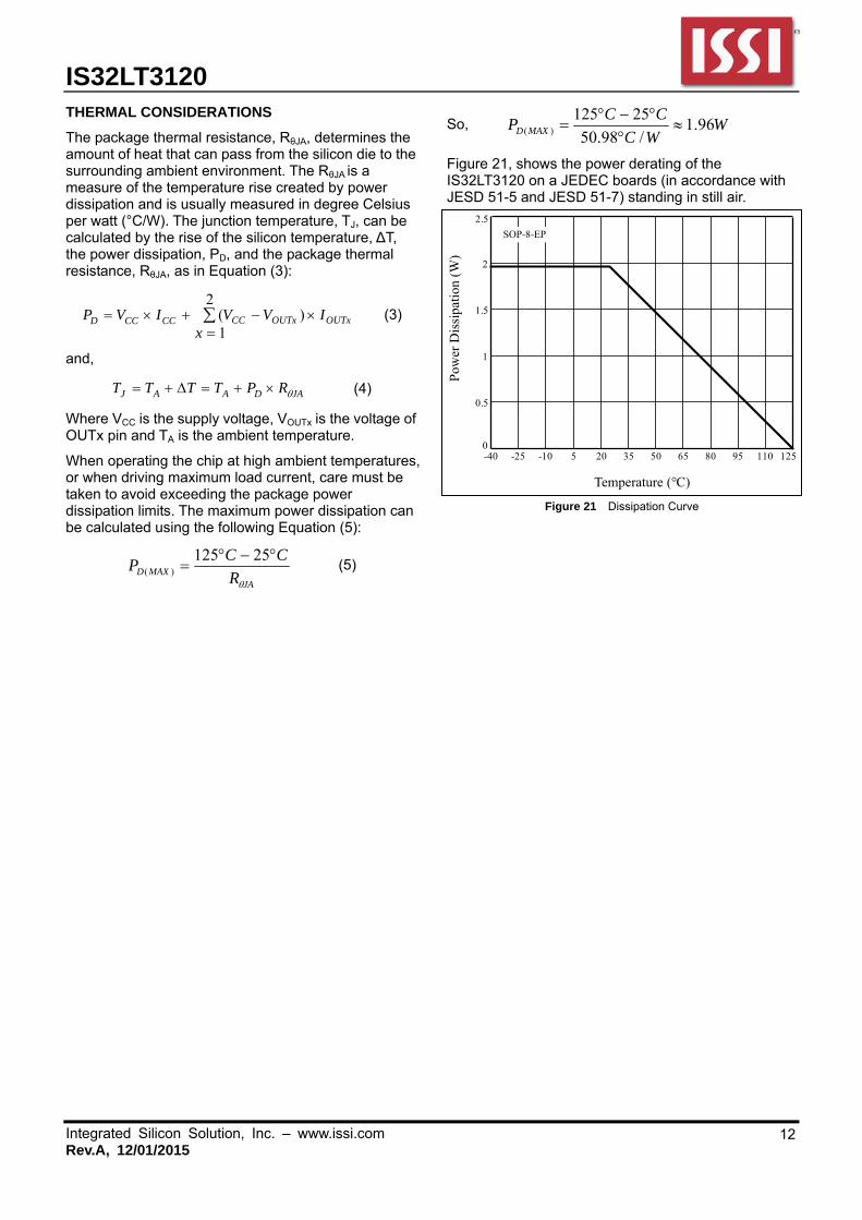
THERMAL CONSIDERATIONS
The package thermal resistance, RθJA, determines the amount of heat that can pass from the silicon die to the surrounding ambient environment. The RθJA is a measure of the temperature rise created by power dissipation and is usually measured in degree Celsius per watt (°C/W). The junction temperature, TJ, can be calculated by the rise of the silicon temperature, ∆T, the power dissipation, PD, and the package thermal resistance, RθJA, as in Equation (3):
2
1)(
xIVVIVP OUTxOUTxCCCCCCD (3)
and,
JADAAJ RPTTTT (4)
Where VCC is the supply voltage, VOUTx is the voltage of OUTx pin and TA is the ambient temperature.
When operating the chip at high ambient temperatures, or when driving maximum load current, care must be taken to avoid exceeding the package power dissipation limits. The maximum power dissipation can be calculated using the following Equation (5):
JAMAXD R
CCP
25125)( (5)
So, WWC
CCP MAXD 96.1
/98.50
25125)(
Figure 21, shows the power derating of the IS32LT3120 on a JEDEC boards (in accordance with JESD 51-5 and JESD 51-7) standing in still air.
0
0.5
1
1.5
2
2.5
Temperature (°C)
Pow
er D
issi
patio
n (W
)-40 -25 -10 5 20 35 50 65 80 95 110 125
SOP-8-EP
Figure 21 Dissipation Curve

IS32LT3120
Integrated Silicon Solution, Inc. – www.issi.com Rev.A, 12/10/2015
13
CLASSIFICATION REFLOW PROFILES
Profile Feature Pb-Free Assembly
Preheat & Soak Temperature min (Tsmin) Temperature max (Tsmax) Time (Tsmin to Tsmax) (ts)
150°C 200°C 60-120 seconds
Average ramp-up rate (Tsmax to Tp) 3°C/second max.
Liquidous temperature (TL) Time at liquidous (tL)
217°C 60-150 seconds
Peak package body temperature (Tp)* Max 260°C
Time (tp)** within 5°C of the specified classification temperature (Tc)
Max 30 seconds
Average ramp-down rate (Tp to Tsmax) 6°C/second max.
Time 25°C to peak temperature 8 minutes max.
Figure 22 Classification Profile

IS32LT3120
Integrated Silicon Solution, Inc. – www.issi.com Rev.A, 12/01/2015
14
PACKAGE INFORMATION SOP-8-EP

IS32LT3120
Integrated Silicon Solution, Inc. – www.issi.com Rev.A, 12/10/2015
15
RECOMMENDED LAND PATTERN
Note:
1. Land pattern complies to IPC-7351.
2. All dimensions in MM.
3. This document (including dimensions, notes & specs) is a recommendation based on typical circuit board manufacturing parameters. Since land pattern design depends on many factors unknown (eg. user’s board manufacturing specs), user must determine suitability for use.
IS32LT3120
Integrated Silicon Solution, Inc. – www.issi.com Rev.A, 12/01/2015
16
REVISION HISTORY
Revision Detail Information Date
A Initial release 2015.12.10