
Is SiC a Game Changer? - · PDF file+ljk hohfwulf euhdngrzq ilhog doorzv orz rq uhvlvwdqfh lq...
88
Center for Power Electronics Systems 7KH %UDGOH\ 'HSDUWPHQW RI (OHFWULFDO DQG &RPSXWHU (QJLQHHULQJ &ROOHJH RI (QJLQHHULQJ 9LUJLQLD 7HFK %ODFNVEXUJ 9LUJLQLD 86$ Is SiC a Game Changer? 'XVKDQ %RUR\HYLFK &KULVWLQD 'L0DULQR &RQJUHVVR %UDVLOHLWR GH (OHFWU{QLFD GH 3RWrQFLD 6RXWKHUQ 3RZHU (OHFWURQLFV &RQIHUHQFH )RUWDOH]D %UD]LO 1RYHPEHU Tutorial: 2XWOLQH ,QWURGXFWLRQ +LJK )UHTXHQF\ DQG +LJK (IILFLHQF\ ± &RPSDULVRQ ZLWK 6L ± &KDUDFWHUL]DWLRQ RI N9 6L& GLVFUHWH WUDQVLVWRUV +LJK 7HPSHUDWXUH ± )RU SRZHU GHQVLW\ LQ QRUPDO WHPSHUDWXUH DPELHQW ± )RU RSHUDWLRQ LQ KLJKWHPSHUDWXUH DPELHQW 0HGLXP 9ROWDJH +LJK 9ROWDJH &RQFOXVLRQV 5HIHUHQFHV 7XWRULDO ,V 6L& D *DPH &KDQJHU" GE 1RYHPEHU
Transcript of Is SiC a Game Changer? - · PDF file+ljk hohfwulf euhdngrzq ilhog doorzv orz rq uhvlvwdqfh lq...

Center for Power Electronics Systems
Is SiC a Game Changer?Tutorial:
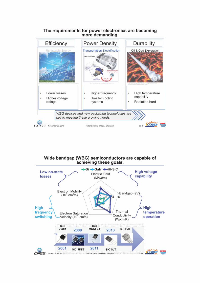
WBG devices and new packaging technologies are key to meeting these growing needs.
Wafer diameter increases.
Vdc
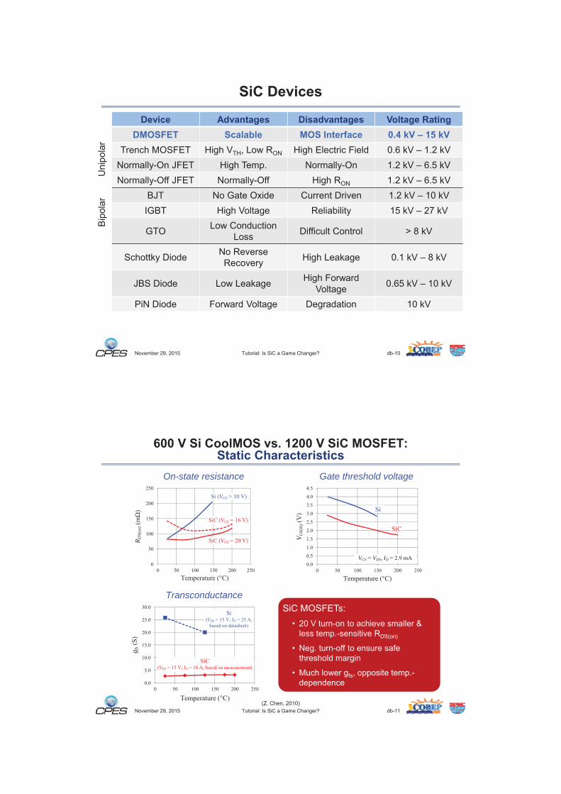
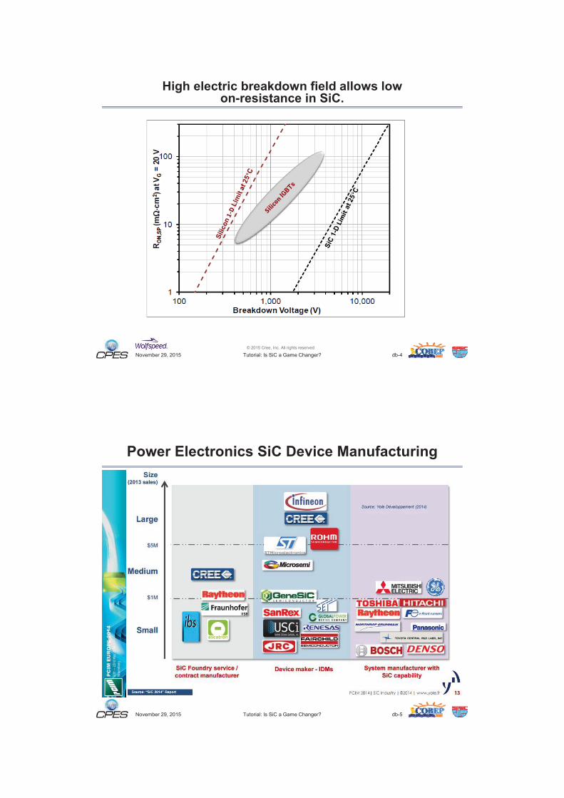
R DS(
on)
VGS
VGS
VGS
On-state resistance
V GS(
th)
VGS VDS ID
Gate threshold voltage
g fs
VDS ID
VDS ID
Transconductance

0 100 200 300 400 500 600
Junction capacitances
Switching energiesTurn-on waveforms
Blue = 25 °C Red = 125 °C
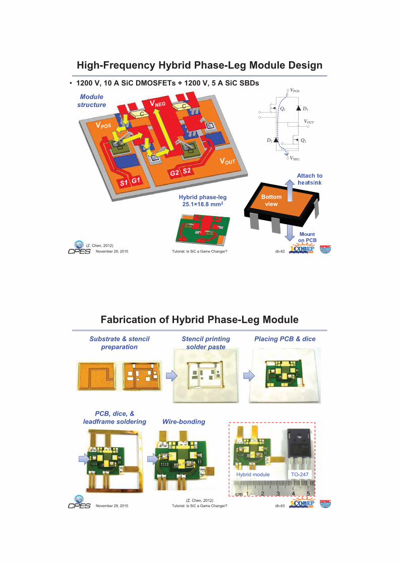
Module features
Module layout Integrated functions
SiCPhase
Leg
Si Phase
Leg
Gate drive w/ Miller clamp
ivov
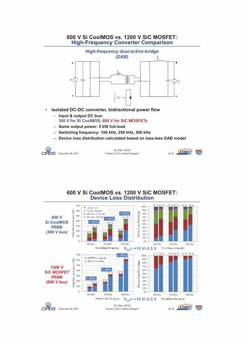
High-frequency dual-active-bridge (DAB)
600 V Si CoolMOS
PEBB(300 V bus)
1200 VSiC MOSFET
PEBB(600 V bus)
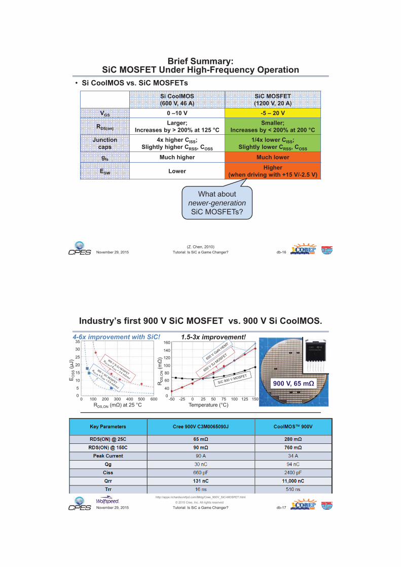
newer-generation
1.5-3x improvement!4-6x improvement with SiC!

220 W LED driver using Wolfspeed C3M
SiC MOSFETs
220 W LED driver using Si SJ MOSFETs

lowerincreased reduces
ID
VDS
ID
VDS
ID
VDS
ID
VDS
SiC
33 kg
15% lower BOM
173 kg

> 10x lower!
f
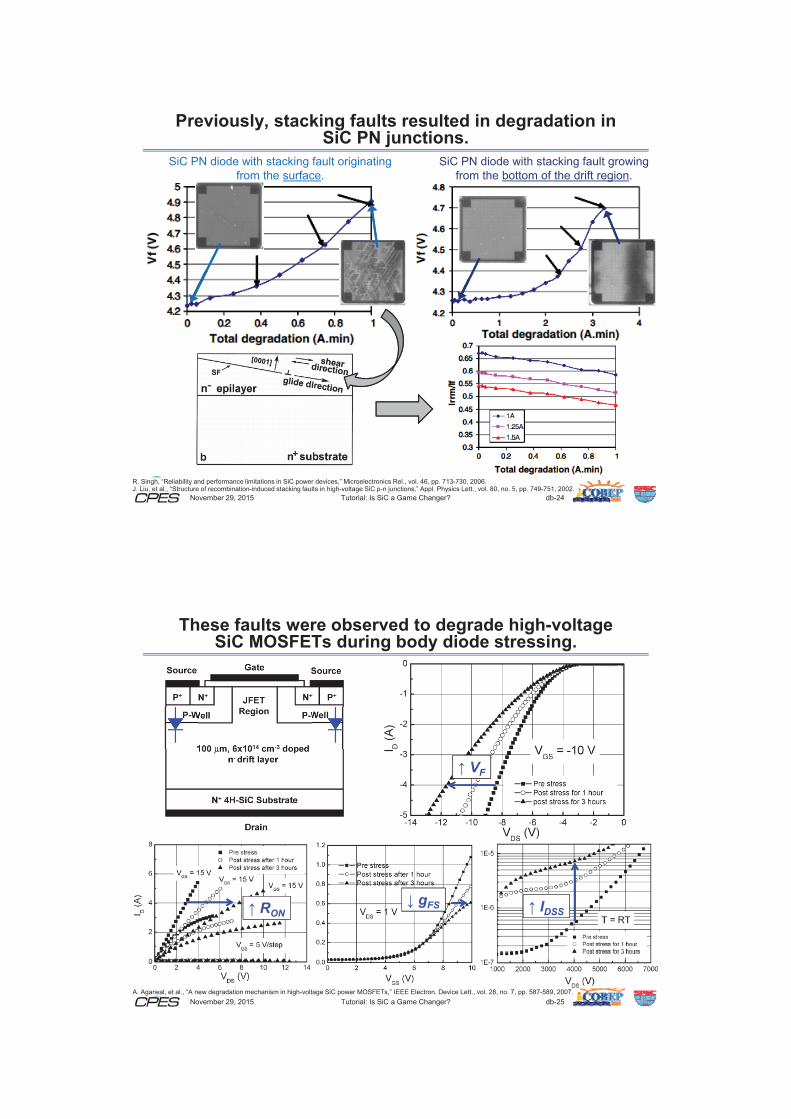
VF
RONgFS IDSS
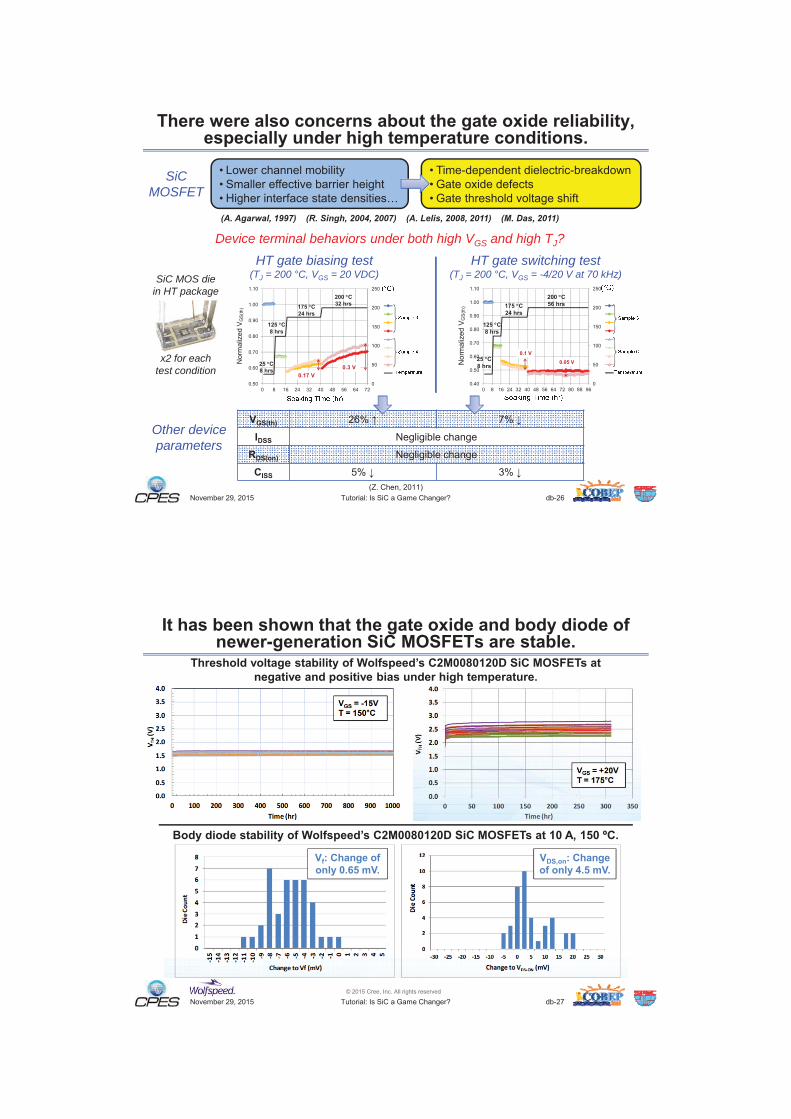
(A. Agarwal, 1997) (R. Singh, 2004, 2007) (A. Lelis, 2008, 2011) (M. Das, 2011)
SiCMOSFET
Device terminal behaviors under both high VGS and high TJ?
HT gate biasing test(TJ = 200 °C, VGS = 20 VDC)
HT gate switching test(TJ = 200 °C, VGS = -4/20 V at 70 kHz)SiC MOS die
in HT package
x2 for each test condition
Other device parameters
Savings with SiC
smaller
lower
less
99 % - Efficient
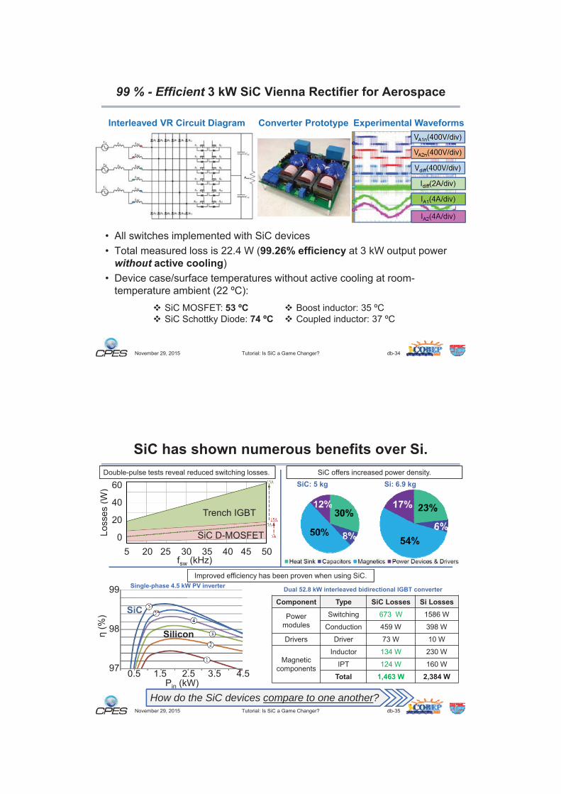
99 % - Efficient
without
How do the SiC devices compare to one another?
200 ºC

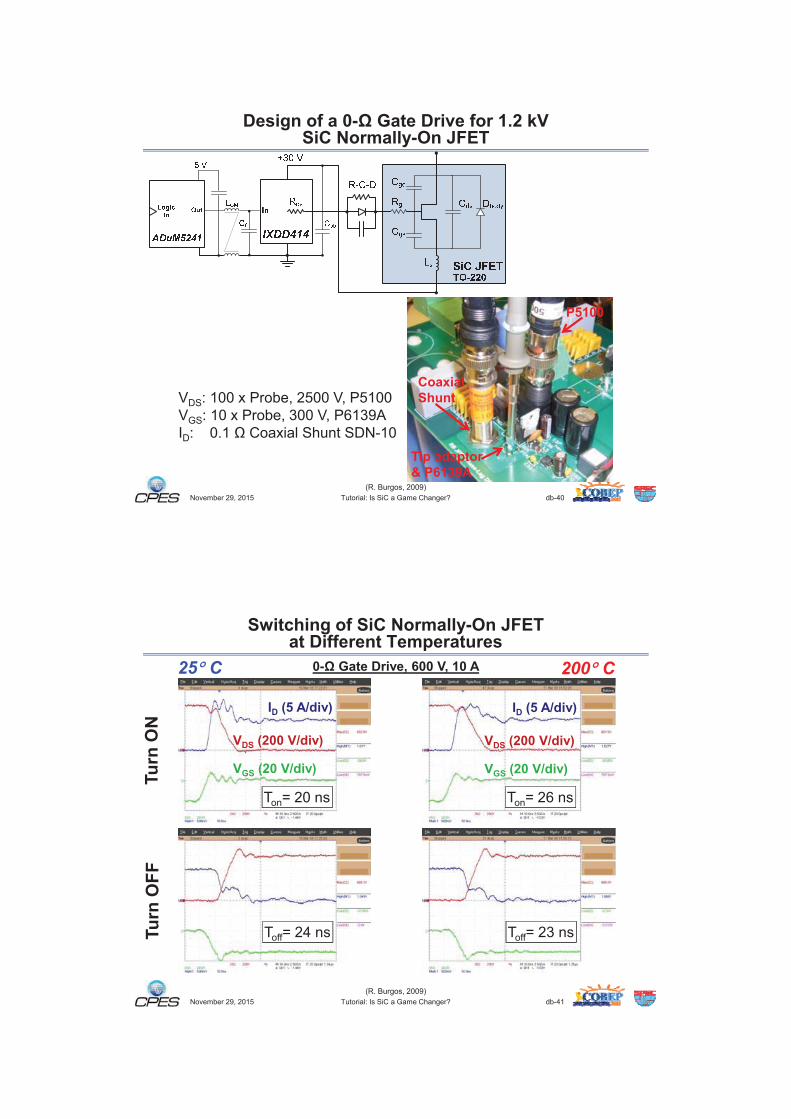
200 C25 C

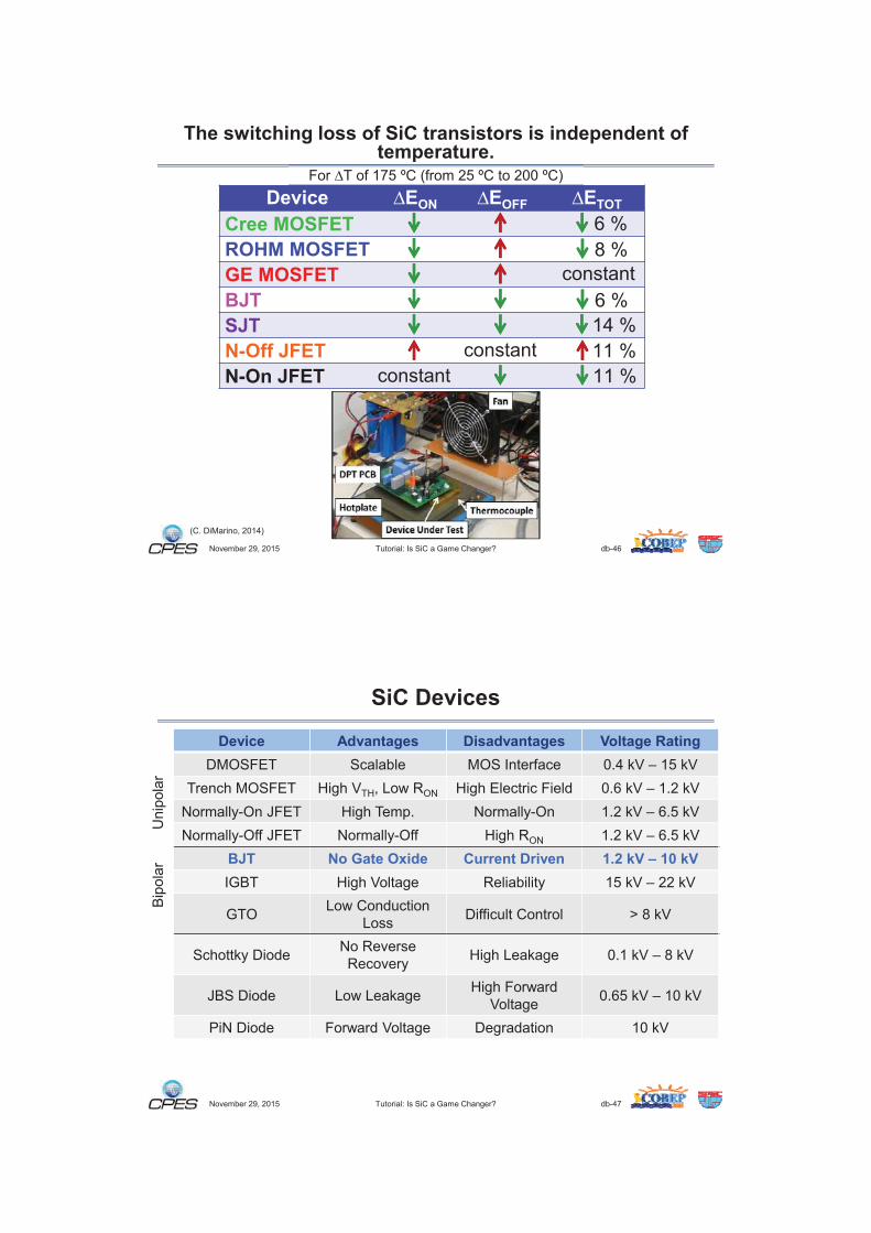
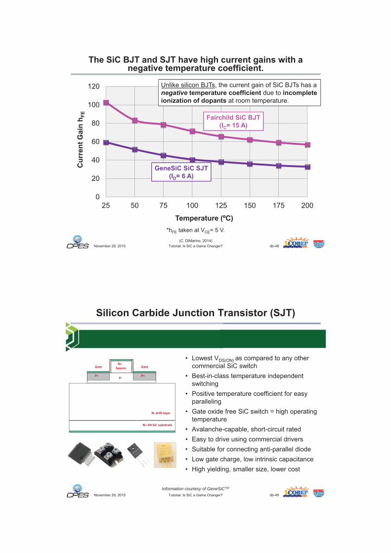
negative
P+P+
N+Source
N drift layer
N+ 4H SiC substrate
GateGate
P
Information courtesy of GeneSiCTM

Information courtesy of GeneSiCTM
2.2x smaller
2.2xsmaller
Information courtesy of GeneSiCTM
4xsmaller
Unlike IGBTs, the SJT does not have a tail current.

Information courtesy of GeneSiCTM

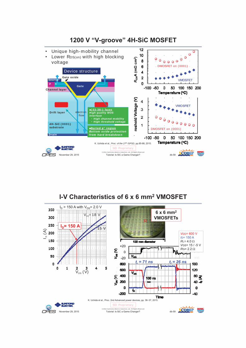
It is expected that the on-resistance can be drastically reduced with the trench gate structure.
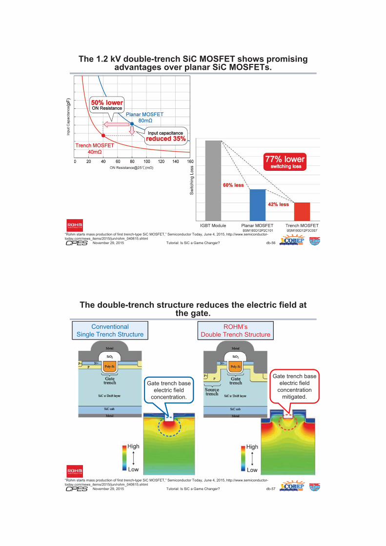
Gate
Gate oxide
Drain
4H-SiC (0001)substrate Buried p+ region
Bottom oxide protection from hard breakdown
electronflow
{03-38-} facesHigh quality MOS interface
High channel mobilityHigh threshold voltage
Drift layer
Channel layer
p nSource
Device structure
Unique high-mobility channelLower RDS(on) with high blocking voltage
Proc. of the 27th ISPSD
DMOSFET on (0001)
DMOSFET on (0001)
SEI Proprietary©2015 Sumitomo Electric Industries, Ltd. All Rights Reserved
SEI Proprietary©2015 Sumitomo Electric Industries, Ltd. All Rights Reserved
VGS=18 V
VDS (V)
I D(A
) 15 VVIR =VR
tr = 71 ns tf = 26 ns
SEI Proprietary©2015 Sumitomo Electric Industries, Ltd. All Rights Reserved
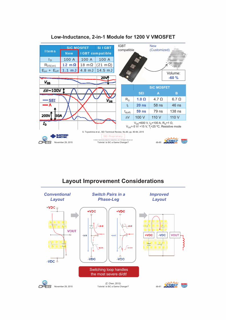
ItemsSiC MOSFET Si IGBT
New IGBT compatible
ID 100 A 100 A 100 ARDS(on) 12 m 18 m (21 m )
Eon + Eoff 1.1 mJ 4.8 mJ 14.5 mJ
Conventional Layout
Switch Pairs in a Phase-Leg
Improved Layout
Q
D
D
Q
VPOS
VNEG
VOUT
Module structure
Substrate & stencil preparation
Stencil printing solder paste
Placing PCB & dice
PCB, dice, & leadframe soldering Wire-bonding
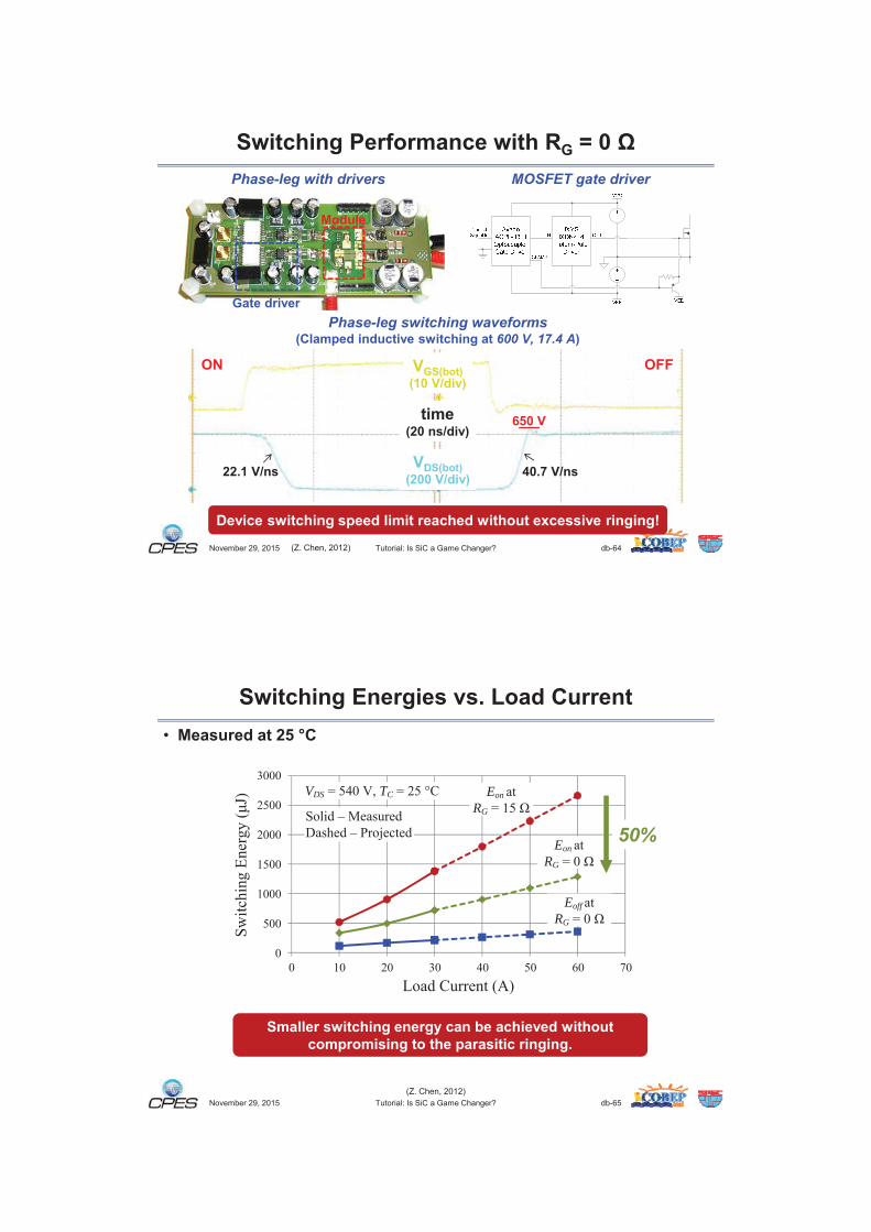
MOSFET gate driverPhase-leg with drivers
Phase-leg switching waveforms600 V, 17.4 A
VDS TC EonRG
EonRG
Eoff RG
50%
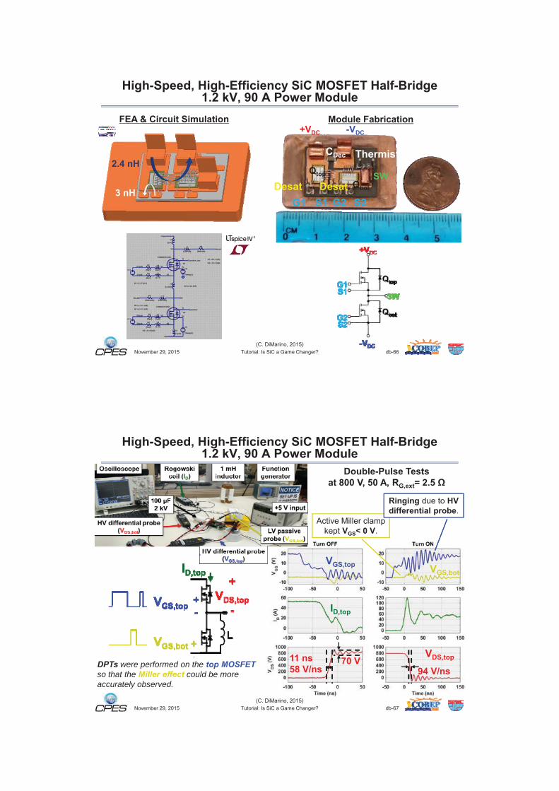
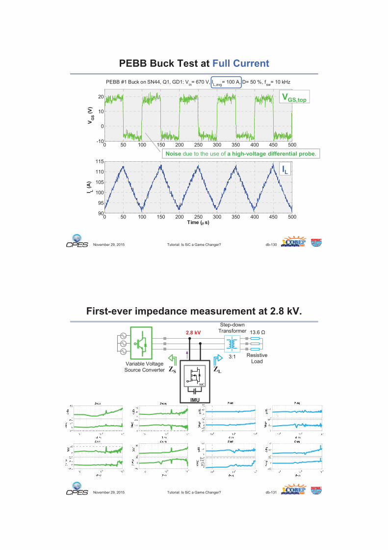
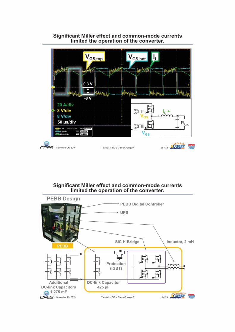
DPTs were performed on the top MOSFET so that the Miller effect could be more accurately observed.
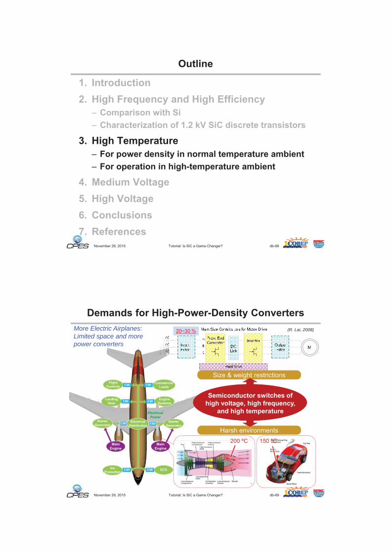
More Electric Airplanes:Limited space and more power converters
(R. Lai, 2008)
VdcVac

Only normally-on JFETs available at the time.
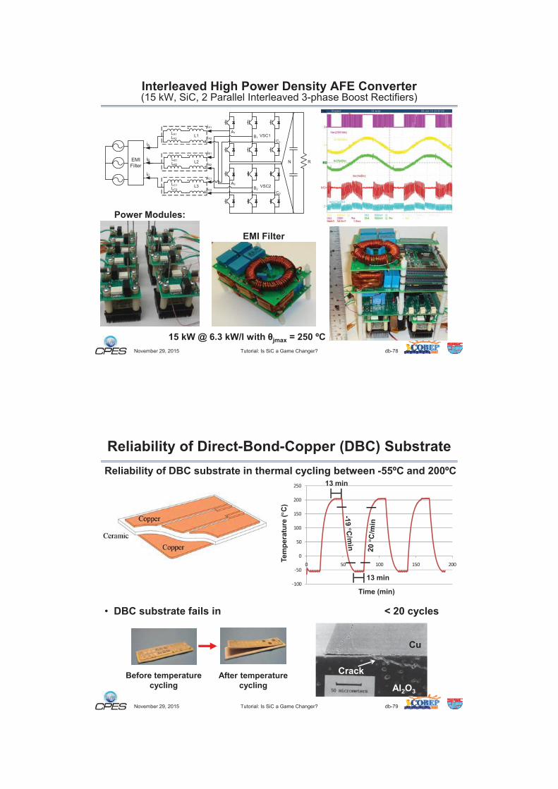
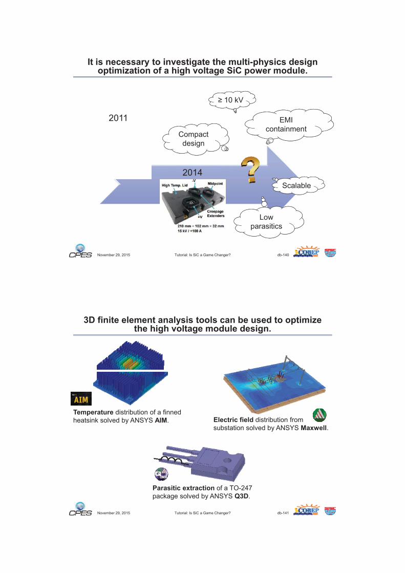
FEA thermal simulation
Continuous operation at 250 ºC


100
50
0
50
100
150
200
250
0 50 100 150 200
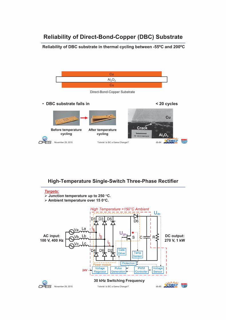
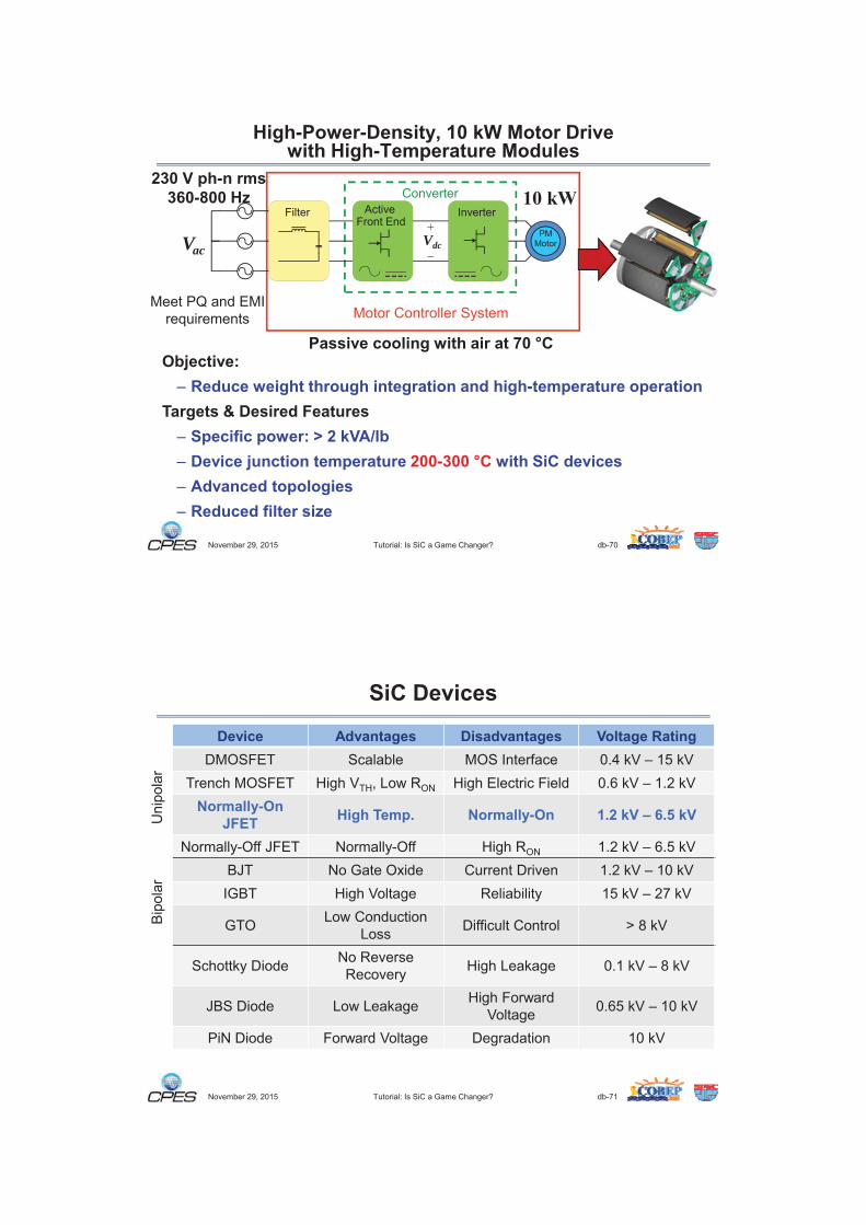
Targets:

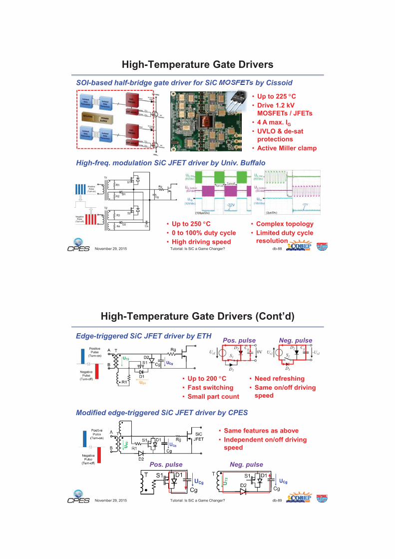
SOI-based half-bridge gate driver for SiC MOSFETs by Cissoid
High-freq. modulation SiC JFET driver by Univ. Buffalo
Edge-triggered SiC JFET driver by ETH Pos. pulse Neg. pulse
Modified edge-triggered SiC JFET driver by CPES
Pos. pulse Neg. pulse
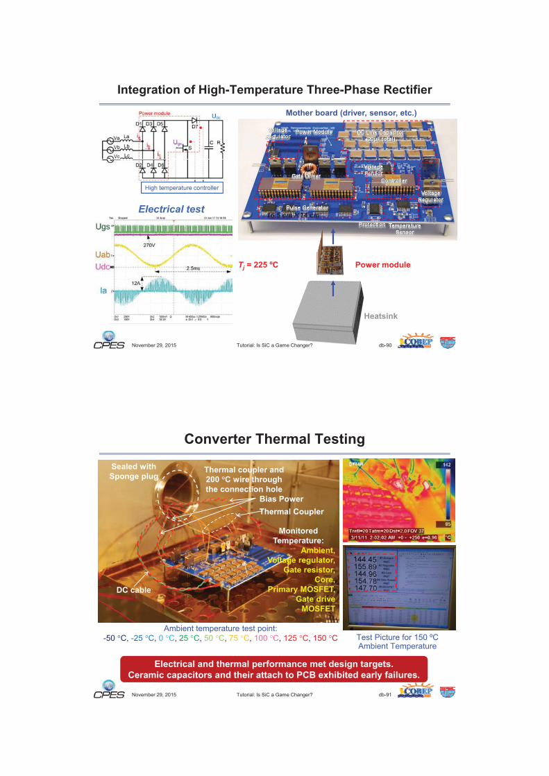
16.5 cm 14 cmElectrical test
Tj

50 kW inverter/rectifier for starter/generatorHigh-temperature and high-power-densityAmbient temperature: 200 – 250 CSwitching frequency: 70 kHz
Target:
VDC
Commercial products(1200 V, 100 A)

Pb95-Sn5
AlN DBC
AlSiC
Al
Electro-less Ni
NuSil R-2188 silicone
Ni-plated Cu
Improved substrate layout to minimize loop inductances
Fabricated module with DC decoupling capacitors
Fast & clean switchingTurn-on Turn-off
Switching Lossis 10-20% of an equivalent IGBT
Module

Test setup
Buck-mode operation Test results at 560 V & 100 kHz
Fabricated module
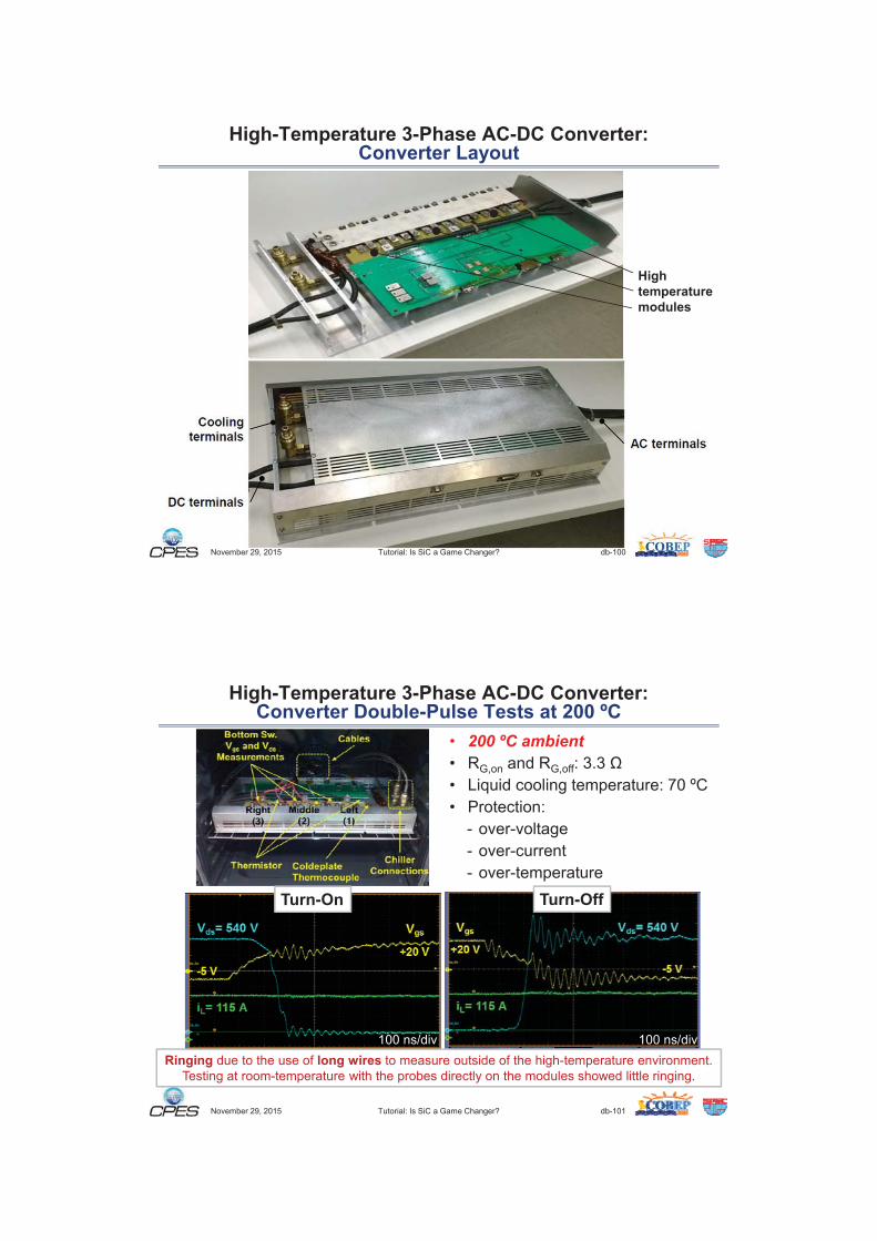
200 ºC ambient
Pareto of IDSSleakage (A)
Pareto of VGSTH shift (%)
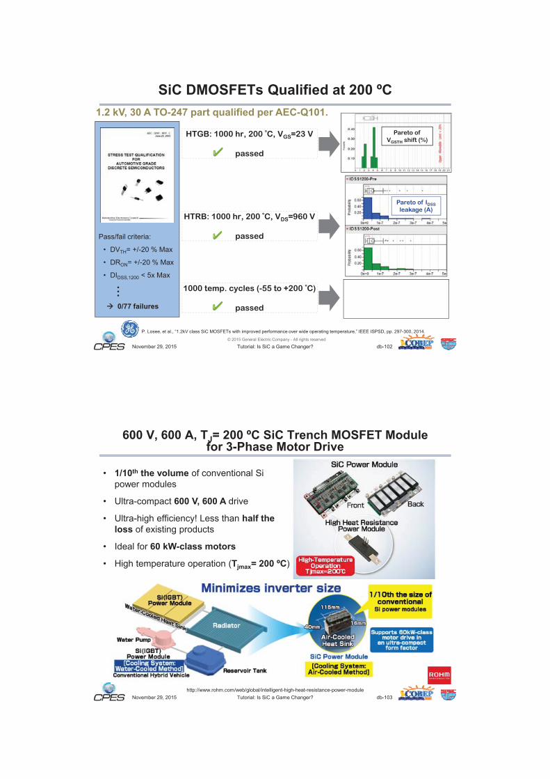
HTGB: 1000 hr, 200 ºC, VGS=23 V
passed
HTRB: 1000 hr, 200 ºC, VDS=960 V
passed
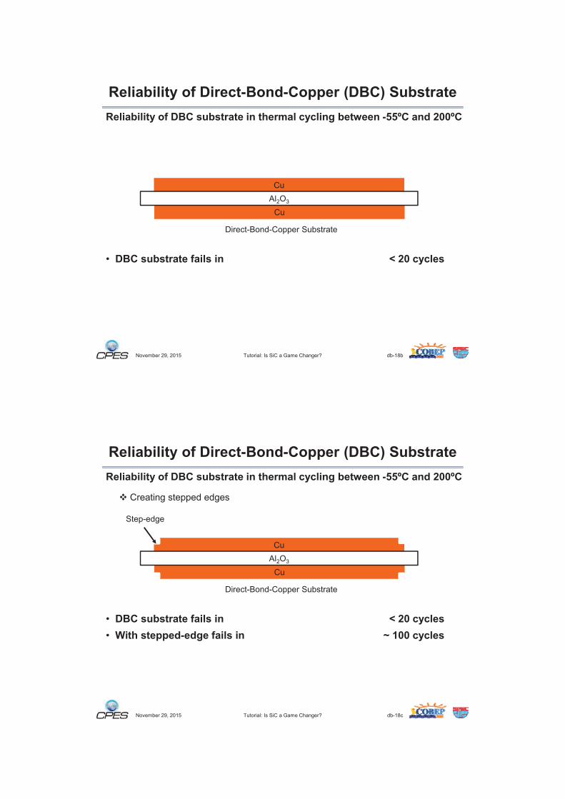
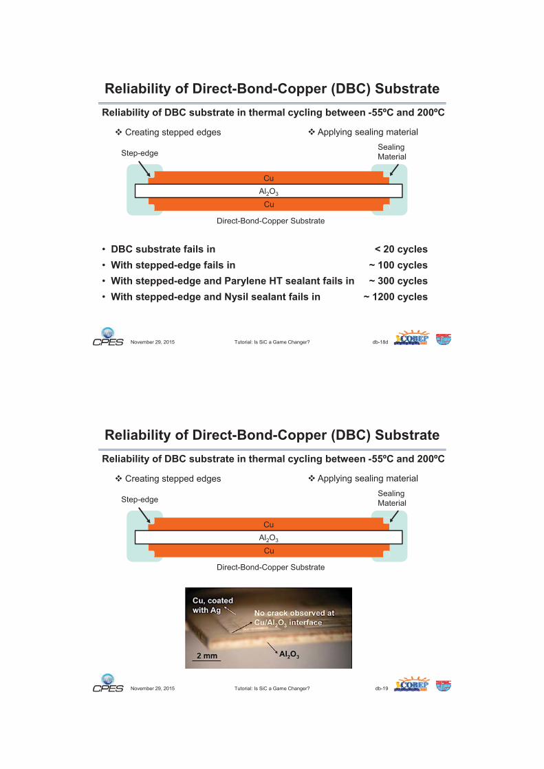
1000 temp. cycles (-55 to +200 ºC)
passed


1.7 kV
POS
NEG
Vdc
Vdc
LO
Grid
Larm
Larm
C
Filter dc
O
arm
armVdc
LODC
BusLarm
Larm
C
Filter 1800
mm
230mm
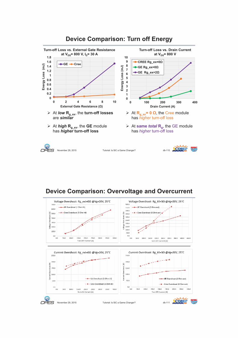
lowsimilar higher
highhigher
totalhigher

SEI Proprietary©2015 Sumitomo Electric Industries, Ltd. All Rights Reserved
DMOSFET I-V
SEI Proprietary©2015 Sumitomo Electric Industries, Ltd. All Rights Reserved
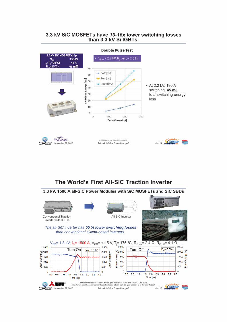
10-15x lower
The all-SiC inverter has 55 % lower switching losses than conventional silicon-based inverters.


10 kV 1.7 kV
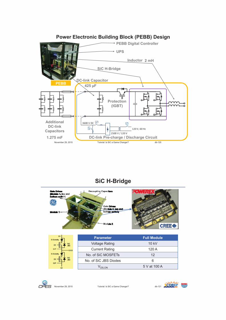
120 V, 60 Hz
2500 V / 120 V
3600 V DC


>10X higher
30 %

increase
reduced
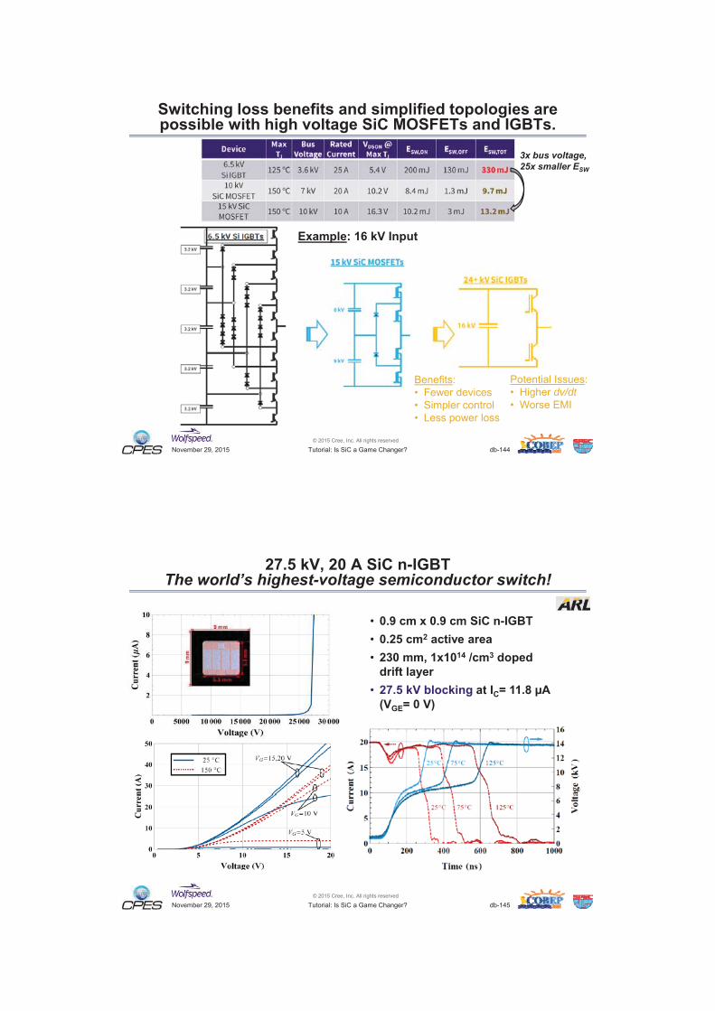
3x bus voltage, 25x smaller ESW
dv/dt
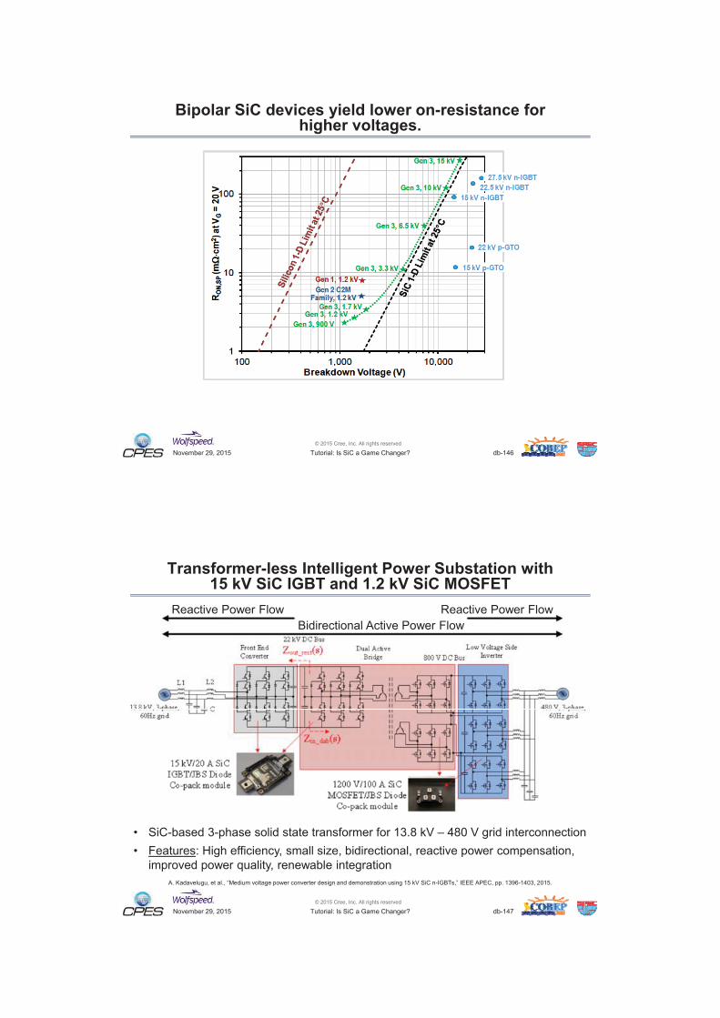
The world’s highest-voltage semiconductor switch!
Information courtesy of GeneSiCTM
Information courtesy of GeneSiCTM

Information courtesy of GeneSiCTM
20 μs

Not a game changer, but a New Game.
Not a game changer, but a New Game.

Int. Conf. Integrated Power Systems
Proc. IMAPs Conf. and Expo. on HiTEN 2013
Proc. Energy Conversion Engineering Conference
Integrated Power Electronics Systems (CIPS)


![5HWXUQ )RUP - · PDF file5(7851 5($621 &2'(6 'lvolnh pdwhuld o 'lvolnh vw\oh 6l]h lv vpdooh u wkdq h[shfwhg 6l]h lv odujhu wkdq h[shfwhg 2 ughuhg pxowlsohv wr frpsduh](https://static.fdocuments.in/doc/165x107/5aa241c67f8b9a84398ccedf/5hwxuq-rup-7851-5621-26-lvolnh-pdwhuld-o-lvolnh-vwoh-6lh-lv-vpdooh-u.jpg)


![S 'PD 1DPH 6L]H ,OOQHVV $FWUDSLG 9LDO ,8 PO PO 9LDO ; 0 ... · &ruh /lvw ) 'ldehwhv 0hoolwxv -dqxdu\ $7&/9/ 1rq 3ursulhwdu\ 'uxj &gh 'pd 'uxj 'hvfulswlrq 3dfn 6l]h 1dph 3dfn 6l]h](https://static.fdocuments.in/doc/165x107/5dd13ea7d6be591ccb64ea64/s-pd-1dph-6lh-ooqhvv-fwudslg-9ldo-8-po-po-9ldo-0-ruh-lvw-ldehwhv.jpg)
