Is Now Part of - ON Semiconductor · © 2014 Fairchild Semiconductor Corporation Rev. 1.2 •...
8
To learn more about ON Semiconductor, please visit our website at www.onsemi.com Is Now Part of ON Semiconductor and the ON Semiconductor logo are trademarks of Semiconductor Components Industries, LLC dba ON Semiconductor or its subsidiaries in the United States and/or other countries. ON Semiconductor owns the rights to a number of patents, trademarks, copyrights, trade secrets, and other intellectual property. A listing of ON Semiconductor’s product/patent coverage may be accessed at www.onsemi.com/site/pdf/Patent-Marking.pdf. ON Semiconductor reserves the right to make changes without further notice to any products herein. ON Semiconductor makes no warranty, representation or guarantee regarding the suitability of its products for any particular purpose, nor does ON Semiconductor assume any liability arising out of the application or use of any product or circuit, and specifically disclaims any and all liability, including without limitation special, consequential or incidental damages. Buyer is responsible for its products and applications using ON Semiconductor products, including compliance with all laws, regulations and safety requirements or standards, regardless of any support or applications information provided by ON Semiconductor. “Typical” parameters which may be provided in ON Semiconductor data sheets and/or specifications can and do vary in different applications and actual performance may vary over time. All operating parameters, including “Typicals” must be validated for each customer application by customer’s technical experts. ON Semiconductor does not convey any license under its patent rights nor the rights of others. ON Semiconductor products are not designed, intended, or authorized for use as a critical component in life support systems or any FDA Class 3 medical devices or medical devices with a same or similar classification in a foreign jurisdiction or any devices intended for implantation in the human body. Should Buyer purchase or use ON Semiconductor products for any such unintended or unauthorized application, Buyer shall indemnify and hold ON Semiconductor and its officers, employees, subsidiaries, affiliates, and distributors harmless against all claims, costs, damages, and expenses, and reasonable attorney fees arising out of, directly or indirectly, any claim of personal injury or death associated with such unintended or unauthorized use, even if such claim alleges that ON Semiconductor was negligent regarding the design or manufacture of the part. ON Semiconductor is an Equal Opportunity/Affirmative Action Employer. This literature is subject to all applicable copyright laws and is not for resale in any manner.
Transcript of Is Now Part of - ON Semiconductor · © 2014 Fairchild Semiconductor Corporation Rev. 1.2 •...

To learn more about ON Semiconductor, please visit our website at www.onsemi.com
Is Now Part of
ON Semiconductor and the ON Semiconductor logo are trademarks of Semiconductor Components Industries, LLC dba ON Semiconductor or its subsidiaries in the United States and/or other countries. ON Semiconductor owns the rights to a number of patents, trademarks, copyrights, trade secrets, and other intellectual property. A listing of ON Semiconductor’s product/patent coverage may be accessed at www.onsemi.com/site/pdf/Patent-Marking.pdf. ON Semiconductor reserves the right to make changes without further notice to any products herein. ON Semiconductor makes no warranty, representation or guarantee regarding the suitability of its products for any particular purpose, nor does ON Semiconductor assume any liability arising out of the application or use of any product or circuit, and specifically disclaims any and all liability, including without limitation special, consequential or incidental damages. Buyer is responsible for its products and applications using ON Semiconductor products, including compliance with all laws, regulations and safety requirements or standards, regardless of any support or applications information provided by ON Semiconductor. “Typical” parameters which may be provided in ON Semiconductor data sheets and/or specifications can and do vary in different applications and actual performance may vary over time. All operating parameters, including “Typicals” must be validated for each customer application by customer’s technical experts. ON Semiconductor does not convey any license under its patent rights nor the rights of others. ON Semiconductor products are not designed, intended, or authorized for use as a critical component in life support systems or any FDA Class 3 medical devices or medical devices with a same or similar classification in a foreign jurisdiction or any devices intended for implantation in the human body. Should Buyer purchase or use ON Semiconductor products for any such unintended or unauthorized application, Buyer shall indemnify and hold ON Semiconductor and its officers, employees, subsidiaries, affiliates, and distributors harmless against all claims, costs, damages, and expenses, and reasonable attorney fees arising out of, directly or indirectly, any claim of personal injury or death associated with such unintended or unauthorized use, even if such claim alleges that ON Semiconductor was negligent regarding the design or manufacture of the part. ON Semiconductor is an Equal Opportunity/Affirmative Action Employer. This literature is subject to all applicable copyright laws and is not for resale in any manner.
www.fairchildsemi.com
© 2014 Fairchild Semiconductor Corporation www.fairchildsemi.com Rev. 1.2 • 3/23/15
AN-9079
SPM® 2 Series Thermal Performance by Mounting Torque
Overview
Semiconductor devices are very sensitive to junction
temperature. As the junction temperature increases, the
operating characteristics of a device alter and the failure rate
increases exponentially. This makes the thermal design of
the package very important in the device development stage
and in applications. In particular, contact pressure or
mounting torque can affect thermal performance. This
application note shows a correlation between the mounting
torque and the thermal resistance.
To gain insight into the device’s thermal performance, it is
common to introduce thermal resistance, which is defined as
the difference in temperature between two adjacent
isothermal surfaces divided by the total power flow between
them. For semiconductor devices, junction temperature, TJ,
and reference temperature, Tx, are typically used. The
amount of power flow is equal to the power dissipation of a
device during operation. The selection of a reference point
is arbitrary, but the hottest spot on the back of a device on
which a heat sink is attached is usually chosen. This is
called junction-to-case thermal resistance, RJC. When the
reference point is an ambient temperature, it is called
junction-to-ambient thermal resistance, RJA. Both are used
for characterization of a device’s thermal performance. RJC
is usually used for a device mounted on a heat-sink, while
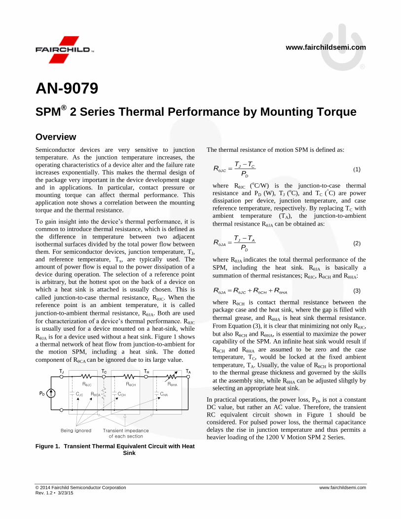
RJA is for a device used without a heat sink. Figure 1 shows
a thermal network of heat flow from junction-to-ambient for
the motion SPM, including a heat sink. The dotted
component of RCA can be ignored due to its large value.
TJ TC TH TA
RθJC RθHA
PD CJC CCH CHA
Transient impedanceof each section
RθCH
RθCA
Being ignored
Figure 1. Transient Thermal Equivalent Circuit with Heat Sink
The thermal resistance of motion SPM is defined as:
D
CJJC
P
TTR
(1)
where RJC (oC/W) is the junction-to-case thermal
resistance and PD (W), TJ (oC), and TC (
°C) are power
dissipation per device, junction temperature, and case
reference temperature, respectively. By replacing TC with
ambient temperature (TA), the junction-to-ambient
thermal resistance RJA can be obtained as:
D
AJJA
P
TTR
(2)
where RJA indicates the total thermal performance of the
SPM, including the heat sink. RJA is basically a
summation of thermal resistances; RJC, RCH and RHA:
HACHJCJA RRRR
(3)
where RCH is contact thermal resistance between the
package case and the heat sink, where the gap is filled with
thermal grease, and RHA is heat sink thermal resistance.
From Equation (3), it is clear that minimizing not only RJC,
but also RCH and RHA, is essential to maximize the power
capability of the SPM. An infinite heat sink would result if
RCH and RHA are assumed to be zero and the case
temperature, TC, would be locked at the fixed ambient
temperature, TA. Usually, the value of RCH is proportional
to the thermal grease thickness and governed by the skills
at the assembly site, while RHA can be adjusted slihgtly by
selecting an appropriate heat sink.
In practical operations, the power loss, PD, is not a constant
DC value, but rather an AC value. Therefore, the transient
RC equivalent circuit shown in Figure 1 should be
considered. For pulsed power loss, the thermal capacitance
delays the rise in junction temperature and thus permits a
heavier loading of the 1200 V Motion SPM 2 Series.
AN-9079 APPLICATION NOTE
© 2013 Fairchild Semiconductor Corporation www.fairchildsemi.com Rev. 1.2 • 3/23/15 2
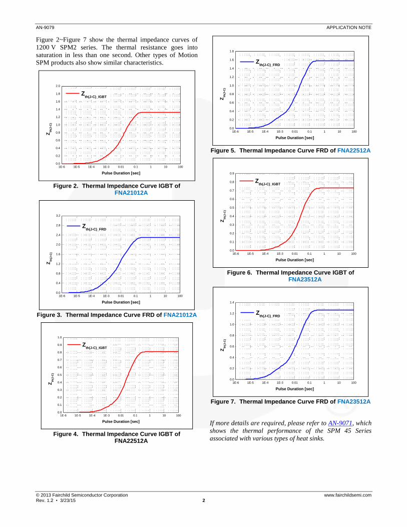
Figure 2~Figure 7 show the thermal impedance curves of
1200 V SPM2 series. The thermal resistance goes into
saturation in less than one second. Other types of Motion
SPM products also show similar characteristics.
1E-6 1E-5 1E-4 1E-3 0.01 0.1 1 10 1000.0
0.2
0.4
0.6
0.8
1.0
1.2
1.4
1.6
1.8
2.0
Zth(J-C)_IGBT
Zth
(J-C
)
Pulse Duration [sec]
Figure 2. Thermal Impedance Curve IGBT of FNA21012A
1E-6 1E-5 1E-4 1E-3 0.01 0.1 1 10 1000.0
0.4
0.8
1.2
1.6
2.0
2.4
2.8
3.2
Zth(J-C)_FRD
Zth
(J-C
)
Pulse Duration [sec]
Figure 3. Thermal Impedance Curve FRD of FNA21012A
1E-6 1E-5 1E-4 1E-3 0.01 0.1 1 10 1000.0
0.1
0.2
0.3
0.4
0.5
0.6
0.7
0.8
0.9
1.0
Zth(J-C)_IGBT
Zth
(J-C
)
Pulse Duration [sec]
Figure 4. Thermal Impedance Curve IGBT of
FNA22512A
1E-6 1E-5 1E-4 1E-3 0.01 0.1 1 10 1000.0
0.2
0.4
0.6
0.8
1.0
1.2
1.4
1.6
1.8
Zth(J-C)_FRD
Zth
(J-C
)
Pulse Duration [sec]
Figure 5. Thermal Impedance Curve FRD of FNA22512A
1E-6 1E-5 1E-4 1E-3 0.01 0.1 1 10 1000.0
0.1
0.2
0.3
0.4
0.5
0.6
0.7
0.8
0.9
Zth(J-C)_IGBT
Zth
(J-C
)
Pulse Duration [sec]
Figure 6. Thermal Impedance Curve IGBT of FNA23512A
1E-6 1E-5 1E-4 1E-3 0.01 0.1 1 10 1000.0
0.2
0.4
0.6
0.8
1.0
1.2
1.4
Zth(J-C)_FRD
Zth
(J-C
)
Pulse Duration [sec]
Figure 7. Thermal Impedance Curve FRD of FNA23512A
If more details are required, please refer to AN-9071, which
shows the thermal performance of the SPM 45 Series
associated with various types of heat sinks.
AN-9079 APPLICATION NOTE
© 2013 Fairchild Semiconductor Corporation www.fairchildsemi.com Rev. 1.2 • 3/23/15 3
Measurement Method of TJ
At the thermal resistance test, TJ, TC (or TA), and PD should
be measured. Since TC, TA, and PD can be measured directly,
the only unknown constant is the junction temperature, TJ.
The Electrical Test Method (ETM) is widely used to
measure the junction temperature. The ETM method is
based on the relationship between forward-drop voltage and
junction temperature. This relationship is an intrinsic
electro-thermal property of semiconductor junctions and is
found to be nearly linear when a constant forward-biased
current (sense current) is applied. This voltage drop of the
junction is called Temperature Sensitive Parameter (TSP).
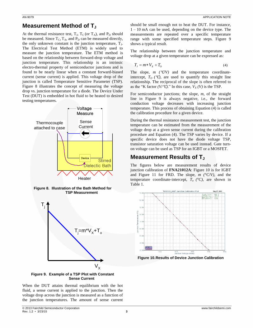
Figure 8 illustrates the concept of measuring the voltage
drop vs. junction temperature for a diode. The Device Under
Test (DUT) is embedded in hot fluid to be heated to desired
testing temperatures.
StirredDielectic Bath
Voltage Measure
Thermocouple
attached to case
Device
Heater
Sense
Current
Figure 8. Illustration of the Bath Method for TSP Measurement
Tj=m*V
X+T
o
Tj
VX
Figure 9. Example of a TSP Plot with Constant Sense Current
When the DUT attains thermal equilibrium with the hot
fluid, a sense current is applied to the junction. Then the
voltage drop across the junction is measured as a function of
the junction temperatures. The amount of sense current
should be small enough not to heat the DUT. For instance,
1 – 10 mA can be used, depending on the device type. The
measurements are repeated over a specific temperature
range with some specified temperature steps. Figure 9
shows a typical result.
The relationship between the junction temperature and
voltage drop at a given temperature can be expressed as:
OXJ TVmT
(4)
The slope, m (℃/V) and the temperature coordinate-
intercept, TO (℃), are used to quantify this straight line
relationship. The reciprocal of the slope is often referred to
as the “K factor (V/℃).” In this case, VX (V) is the TSP.
For semiconductor junctions; the slope, m, of the straight
line in Figure 9 is always negative, i.e., the forward
conduction voltage decreases with increasing junction
temperature. This process of obtaining Equation (4) is called
the calibration procedure for a given device.
During the thermal resistance measurement test, the junction
temperature can be estimated from the measurement of the
voltage drop at a given sense current during the calibration
procedure and Equation (4). The TSP varies by device. If a
specific device does not have the diode voltage TSP,
transistor saturation voltage can be used instead. Gate turn-
on voltage can be used as TSP for an IGBT or a MOSFET.
Measurement Results of TJ
The figures below are measurement results of device
junction calibration of FNA21012A: Figure 10 is for IGBT
and Figure 11 for FRD. The slope, m (°C/V), and the
temperature coordinate-intercept, To (°C), are shown in
Table 1.
Figure 10. Results of Device Junction Calibration
AN-9079 APPLICATION NOTE
© 2013 Fairchild Semiconductor Corporation www.fairchildsemi.com Rev. 1.2 • 3/23/15 4
Figure 11. Results of Device Junction Calibration
Table 1. m (°C/V) and Temperature Coordinate-Intercept, To (V) for FNA21012A
Device m(°C/V) TO(°C) Sensing Current
FNA21012A IGBT -460.0 282.5
10 mA FRD -475.2 305.3
Thermal Resistance, RJC
The thermal resistance from junction to case, RJC, can be
calculated from Equation (1). Usaully, the themal resistance
is measured at two different points, package center and chip
center. Table 2 shows values measured at chip center.
Table 2. RJC: Thermal Resistance, °C/W
Classification SPL P(W) TJ TC RJC
FNA21012A Chip Center
#1 62.28 121.10 60.40 0.97
#2 62.28 121.80 61.80 0.97
#3 62.28 120.50 60.10 0.96
The RJC on SPM product datasheets is based on chip center
values and has margin to cover manufacturing variations.
Thermal Performance by Mounting Torque
Power devices are very sensitive to junction temperature. As
the junction temperature increases, the operating
characteristics of a device alter and the failure rate increases
exponentially. Contact pressure and mounting torque may
affect the thermal performance.
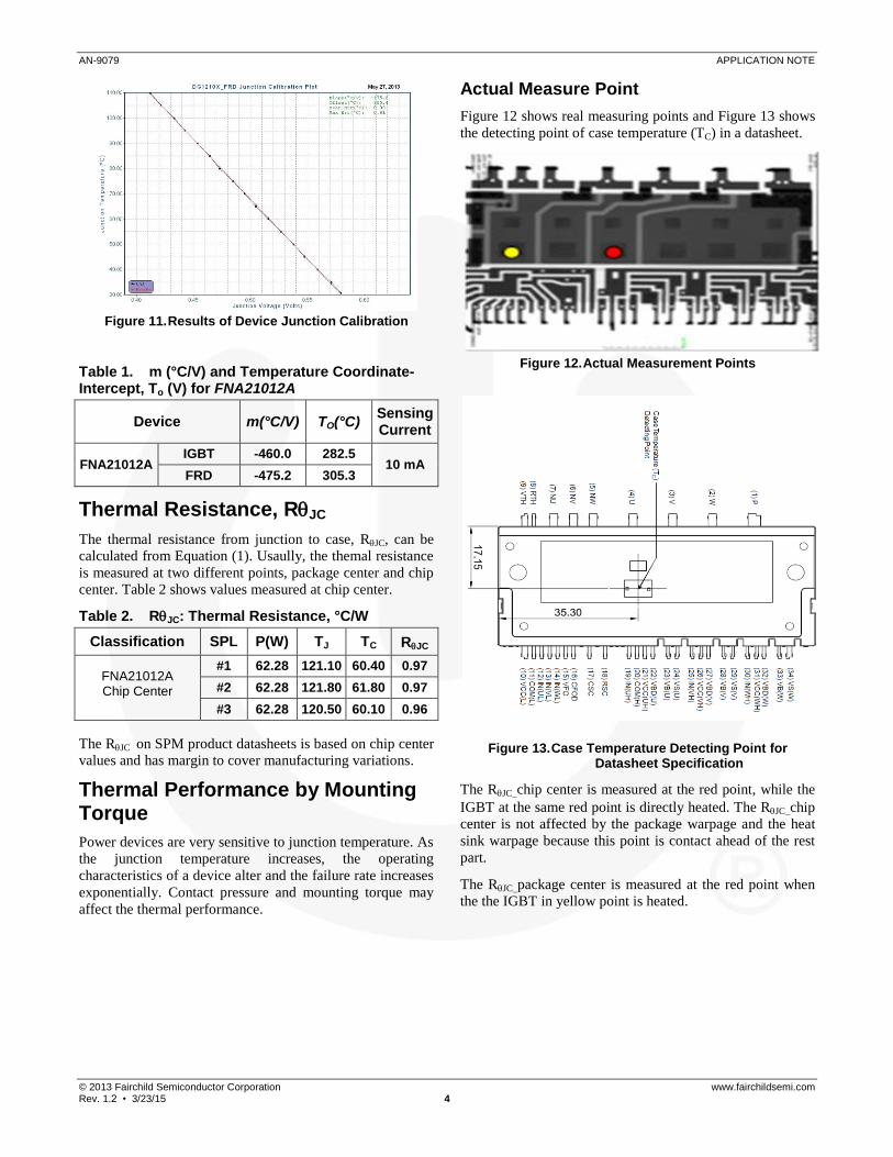
Actual Measure Point
Figure 12 shows real measuring points and Figure 13 shows
the detecting point of case temperature (TC) in a datasheet.
Figure 12. Actual Measurement Points
Figure 13. Case Temperature Detecting Point for Datasheet Specification
The RJC_chip center is measured at the red point, while the
IGBT at the same red point is directly heated. The RJC_chip
center is not affected by the package warpage and the heat
sink warpage because this point is contact ahead of the rest
part.
The RJC_package center is measured at the red point when
the the IGBT in yellow point is heated.
AN-9079 APPLICATION NOTE
© 2013 Fairchild Semiconductor Corporation www.fairchildsemi.com Rev. 1.2 • 3/23/15 5
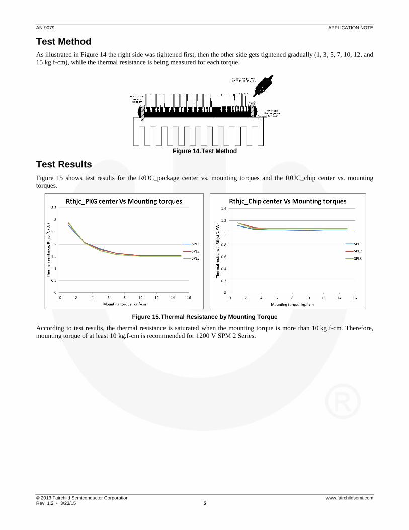
Test Method
As illustrated in Figure 14 the right side was tightened first, then the other side gets tightened gradually (1, 3, 5, 7, 10, 12, and
15 kg.f-cm), while the thermal resistance is being measured for each torque.
Figure 14. Test Method
Test Results
Figure 15 shows test results for the RJC_package center vs. mounting torques and the RJC_chip center vs. mounting
torques.
Figure 15. Thermal Resistance by Mounting Torque
According to test results, the thermal resistance is saturated when the mounting torque is more than 10 kg.f-cm. Therefore,
mounting torque of at least 10 kg.f-cm is recommended for 1200 V SPM 2 Series.
AN-9079 APPLICATION NOTE
© 2013 Fairchild Semiconductor Corporation www.fairchildsemi.com Rev. 1.2 • 3/23/15 6
Related Resources
AN-9071 – Smart Power Module-SPM™ in μMini DIP SPM Thermal Performance Information
AN-9075 – 1200V Motion SPM®
2 Series, User’s Guide
AN-9076 – New SPM®
2 Package, Mounting Guide
DISCLAIMER FAIRCHILD SEMICONDUCTOR RESERVES THE RIGHT TO MAKE CHANGES WITHOUT FURTHER NOTICE TO ANY PRODUCTS HEREIN TO IMPROVE RELIABILITY, FUNCTION, OR DESIGN. FAIRCHILD DOES NOT ASSUME ANY LIABILITY ARISING OUT OF THE APPLICATION OR USE OF ANY PRODUCT OR CIRCUIT DESCRIBED HEREIN; NEITHER DOES IT CONVEY ANY LICENSE UNDER ITS PATENT RIGHTS, NOR THE RIGHTS OF OTHERS. LIFE SUPPORT POLICY FAIRCHILD’S PRODUCTS ARE NOT AUTHORIZED FOR USE AS CRITICAL COMPONENTS IN LIFE SUPPORT DEVICES OR SYSTEMS WITHOUT THE EXPRESS WRITTEN APPROVAL OF THE PRESIDENT OF FAIRCHILD SEMICONDUCTOR CORPORATION. As used herein: 1. Life support devices or systems are devices or systems which, (a) are intended for surgical implant into the body, or (b) support or
sustain life, or (c) whose failure to perform when properly used in accordance with instructions for use provided in the labeling, can be reasonably expected to result in significant injury to the user.
2. A critical component is any component of a life support device or system whose failure to perform can be reasonably expected to cause the failure of the life support device or system, or to affect its safety or effectiveness.
www.onsemi.com1
ON Semiconductor and are trademarks of Semiconductor Components Industries, LLC dba ON Semiconductor or its subsidiaries in the United States and/or other countries.ON Semiconductor owns the rights to a number of patents, trademarks, copyrights, trade secrets, and other intellectual property. A listing of ON Semiconductor’s product/patentcoverage may be accessed at www.onsemi.com/site/pdf/Patent−Marking.pdf. ON Semiconductor reserves the right to make changes without further notice to any products herein.ON Semiconductor makes no warranty, representation or guarantee regarding the suitability of its products for any particular purpose, nor does ON Semiconductor assume any liabilityarising out of the application or use of any product or circuit, and specifically disclaims any and all liability, including without limitation special, consequential or incidental damages.Buyer is responsible for its products and applications using ON Semiconductor products, including compliance with all laws, regulations and safety requirements or standards,regardless of any support or applications information provided by ON Semiconductor. “Typical” parameters which may be provided in ON Semiconductor data sheets and/orspecifications can and do vary in different applications and actual performance may vary over time. All operating parameters, including “Typicals” must be validated for each customerapplication by customer’s technical experts. ON Semiconductor does not convey any license under its patent rights nor the rights of others. ON Semiconductor products are notdesigned, intended, or authorized for use as a critical component in life support systems or any FDA Class 3 medical devices or medical devices with a same or similar classificationin a foreign jurisdiction or any devices intended for implantation in the human body. Should Buyer purchase or use ON Semiconductor products for any such unintended or unauthorizedapplication, Buyer shall indemnify and hold ON Semiconductor and its officers, employees, subsidiaries, affiliates, and distributors harmless against all claims, costs, damages, andexpenses, and reasonable attorney fees arising out of, directly or indirectly, any claim of personal injury or death associated with such unintended or unauthorized use, even if suchclaim alleges that ON Semiconductor was negligent regarding the design or manufacture of the part. ON Semiconductor is an Equal Opportunity/Affirmative Action Employer. Thisliterature is subject to all applicable copyright laws and is not for resale in any manner.
PUBLICATION ORDERING INFORMATIONN. American Technical Support: 800−282−9855 Toll FreeUSA/Canada
Europe, Middle East and Africa Technical Support:Phone: 421 33 790 2910
Japan Customer Focus CenterPhone: 81−3−5817−1050
www.onsemi.com
LITERATURE FULFILLMENT:Literature Distribution Center for ON Semiconductor19521 E. 32nd Pkwy, Aurora, Colorado 80011 USAPhone: 303−675−2175 or 800−344−3860 Toll Free USA/CanadaFax: 303−675−2176 or 800−344−3867 Toll Free USA/CanadaEmail: [email protected]
ON Semiconductor Website: www.onsemi.com
Order Literature: http://www.onsemi.com/orderlit
For additional information, please contact your localSales Representative
© Semiconductor Components Industries, LLC