IRPS2008 Gaddi Haase P5 Dp2
19
AN ALTERNATIVE MODEL FOR INTERCONNECT LOW-K DIELECTRIC LIFETIME DEPENDENCE ON VOLTAGE Gaddi S. Haase Texas Instruments Dallas, TX, USA T EXAS I NSTRUM ENTS
-
Upload
guest3b6d2b -
Category
Education
-
view
320 -
download
0
Transcript of IRPS2008 Gaddi Haase P5 Dp2

AN ALTERNATIVE MODEL FOR INTERCONNECT LOW-K DIELECTRIC LIFETIME
DEPENDENCE ON VOLTAGE
Gaddi S. Haase
Texas Instruments
Dallas, TX, USA
TEXAS INSTRUMENTS

2
Purpose• As interconnect metal line-pitch shrinks, we
need to refine BEOL low-k dielectric lifetime-prediction methodologies.
• Our previous work removed line-spacing variations effects from accelerated test data, to improve lifetime predictions.
• Next, the models for lifetime-dependence on stress-voltage need to be re-evaluated.
• We also need to figure out what is the actual mode of failure at operating voltages: – Hard breakdown?– Stress-induced leakage, until the circuit fails?– Increase in k or dielectric absorption that would fail the
circuit?
3
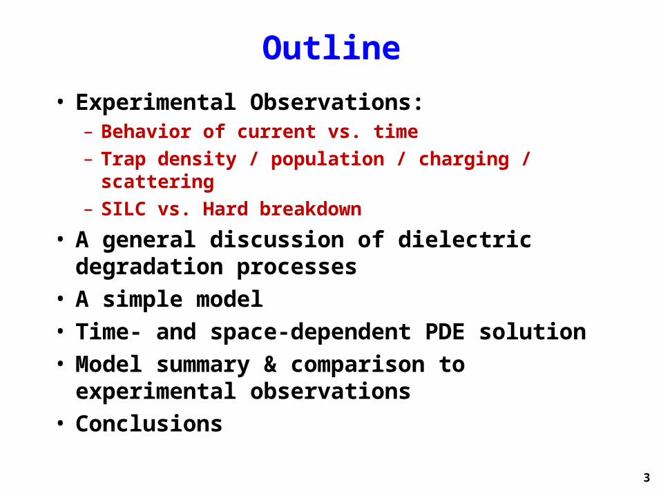
Outline
• Experimental Observations:– Behavior of current vs. time– Trap density / population / charging / scattering– SILC vs. Hard breakdown
• A general discussion of dielectric degradation processes
• A simple model• Time- and space-dependent PDE solution• Model summary & comparison to experimental
observations• Conclusions

4
Low-k dielectric breakdown tests• Constant voltage stress, or V-ramp to breakdown
• Current falls before leakage increases at constant voltage• Leakage is lower when ramping V at a slower rate• Slow charging of traps? Slow trap creation?
1.E-07
1.E-06
1.E-05
0.1 1 10 100 1000 10000
Constant-Voltage Stress Time (s) Stress time (s)
Lea
kag
e (l
og
sca
le)
1.E-09
1.E-08
1.E-07
1.E-06
1.E-05
1.E-04
0 20 40 60
Voltage between comb and serpent (V)
Lea
kag
e C
urr
ent (
A)
100 mV / 1770ms steps
100mV / 170 ms steps
Temp. 105 C

5
Current decrease: Slow trap-charging?
Test under alternating polarity
Stre
ss v
olta
ge
time
• Fast charging or scattering
• Trap density changes
6
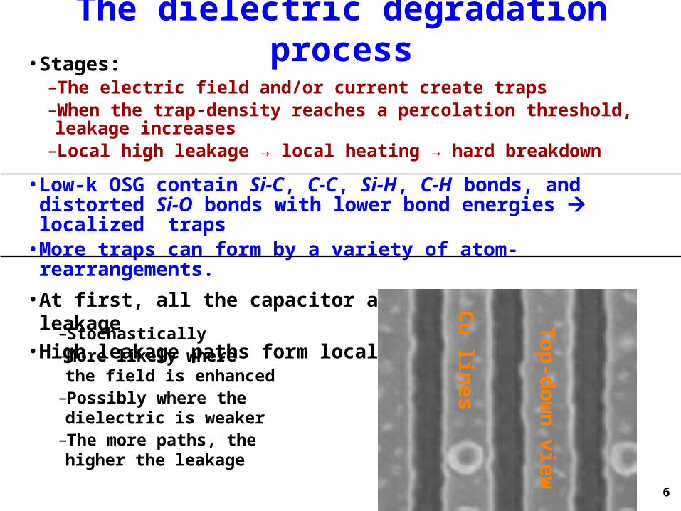
The dielectric degradation process• Stages:
–The electric field and/or current create traps–When the trap-density reaches a percolation threshold, leakage increases
–Local high leakage → local heating → hard breakdown
• Low-k OSG contain Si-C, C-C, Si-H, C-H bonds, and distorted Si-O bonds with lower bond energies localized traps
• More traps can form by a variety of atom-rearrangements.
• At first, all the capacitor area contributes to the leakage
• High leakage paths form locally:
–Stochastically–More likely where the field is enhanced
–Possibly where the dielectric is weaker
–The more paths, the higher the leakage
To
p-d
ow
n view
Cu
lines

7
The dielectric degradation process• Test procedure – compensating for spacing variations between DUTs:
–First 100ms at a set constant current to record the voltage.–Stress at constant voltage= 10% above the recorded voltage.
The rising part of the I-t curve depends on the nature of the percolation paths that open between the electrodes.
1.E-07
1.E-06
1.E-05
1.E-04
0.1 10 1000 100000
Time (s)
Le
ak
ag
e c
urr
en
t (A
)
125nm
105nm
85nm
70nm
Actual stress: E=~4.1–4.4 MV/cm
(Lower spacing required a slightly higher field)
Drawn spacing (on the same wafer):
125nm
105nm
85nm
70nm
10-4
10-5
10-6
10-7
10-1 10 103 105

8
• Dielectric relaxation type test: I vs. t after zeroing a DC stress.
• If after zeroing the stress, most current comes from traps, the trap density does not increase much during stress.
Trap generation during stress
1.E-13
1.E-12
1.E-11
0 5 10
Relaxation time (s)
Re
lax
ati
on
cu
rre
nt
(A)
0.E+00
1.E-12
2.E-12
3.E-12
4.E-12
0 5000 10000 15000
Total stress time (s)
Rel
axat
ion
-cu
rren
t a
fter
st
ress
inte
rup
tio
n (
A)
1.0 sec delay
4.5 sec delay
7 per. Mov. Avg.(4.5 sec delay)6 per. Mov. Avg.(4.5 sec delay)
Rel
axat
ion-
curr
ent a
fter s
tres
s in
terr
uptio
n (p
A)
4
3
2
1
0
9
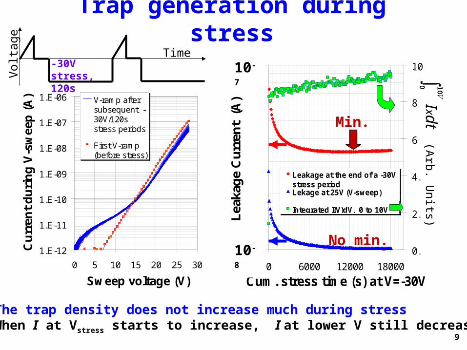
Trap generation during stress
1.E-12
1.E-11
1.E-10
1.E-09
1.E-08
1.E-07
1.E-06
0 5 10 15 20 25 30
Sweep voltage (V)
Cu
rren
t d
uri
ng
V-s
wee
p (
A) V-ramp after
subsequent -30V/120sstress periods
First V-ramp(before stress)
Time
V
olta
ge
-30V stress, 120s
•The trap density does not increase much during stress•When I at Vstress starts to increase, I at lower V still decreases.
1.E-08
1.E-07
0 6000 12000 18000
Cum. stress time (s) at V=-30V
Lea
kag
e C
urr
ent
(A
)0.E+00
2.E-11
4.E-11
6.E-11
8.E-11
1.E-10
Leakage at the end of a -30Vstress periodLekage at 25V (V-sweep)
Integrated I(V)dV, 0 to 10V
Min.
No min.10-810-8
10-7
1.E-08
1.E-07
0 6000 12000 18000
0.E+00
2.E-11
4.E-11
6.E-11
8.E-11
1.E-10
Ixdt (Arb. U
nits)

10
Stress-induced leakage
• The leakage at 1.2V emerges sharply from the noise only after ~10x t(min.curr.@Vstress).
• Only at the last ~1000s the 1.2V leakage grows at the same rel. rate as the leakage @Vstress
Drawn line-spacing: 125nm
1.E-14
1.E-12
1.E-10
1.E-08
1.E-06
1.E-04
10 100 1000 10000
Cumulative StressTime (s)
Lea
kag
e cu
rren
t (A
)
Current during a constant +48V stress
Current at the end of 1s@+1.2V stress-interruption periods.

11
Model: Trap generation
Average electron energy:
Two extreme options to treat the e- energy:• A shift in the center of the e--energy distribution, represented by lowering Ea • The temperature Te is the electron temperature > Twafer
• A parameter p is the fraction of the e--energy that is represented by e--temperature rise, while (1-p) is the fraction that is represented by Te=Twafer and Ea,eff < Ea .
eb
effascate
Trap
Tk
EltxJ
t
tx ,1 exp,,The rate
of trap generation
Electron flux Average distance between traps
),( txFqlEnergy scate
31
, txl Trapscat
Drift between collisions with traps
Ea is the activation energy for a new trap formation

12
Model: Charge and Field
The total electron density (trapped and mobile) txJ
t
txe
Total ,,
txqtxV Total ,,
txVtxF ,,
The continuity eq.
Poisson eq.
Electron flux
Field
txtxTk
Etx
TrapTotal
b
effTrapTotal
Mobile
,,
exp, ,
The mobile electron-density due to thermal excitation out of the traps:
When the traps are full

13
Model: LeakageElectron flux
txDtxtxVtxJ MobileMobTunnelMobileee ,,,,
A portion of the trapped electrons can tunnel between traps at high field and high trap density, which leads to breakdown:
23
23
*
),(3
24exp effTrapTrapMobileTotalmobTunnel lFqEE
txqF
m
effl is the width of a trapezoidal barrier
0
23*
, 3
24expexp,0
F
qm
Tk
qNtx B
b
BmetaleTotal
At the cathode, the available electron density is controlled by FN tunneling and thermal injection into the dielectric:
Diffusion Coef.Median drift velocity
14
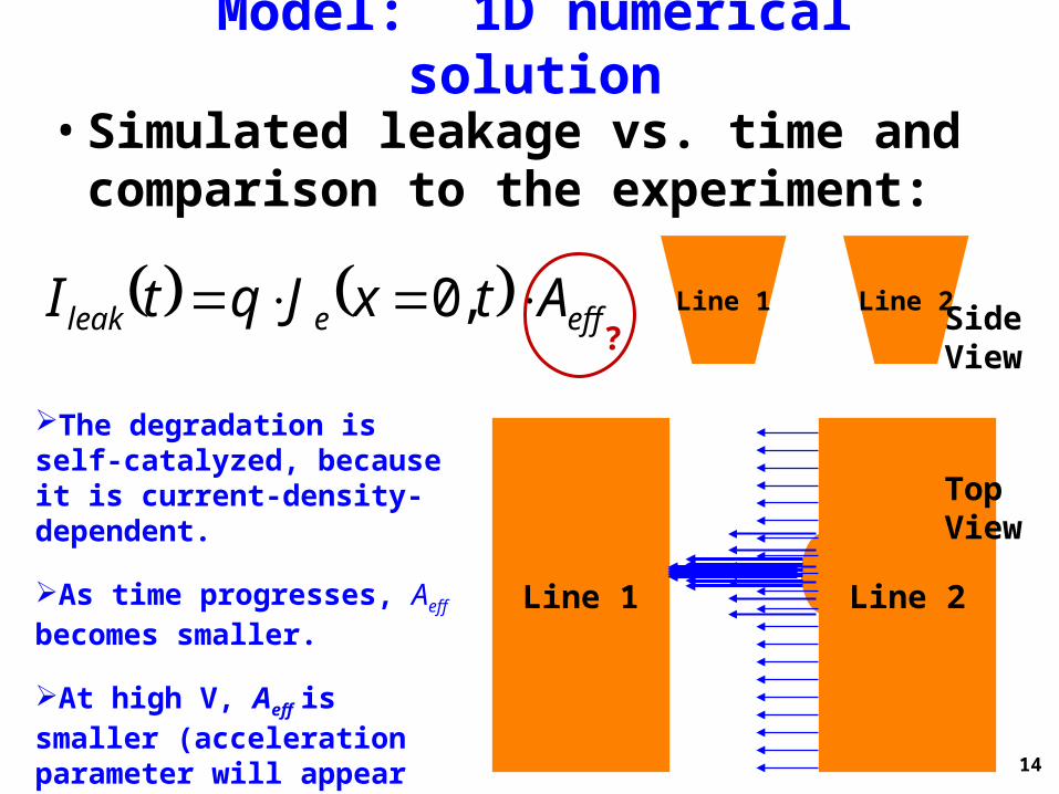
Model: 1D numerical solution
effeleak AtxJqtI ,0
Line 1 Line 2
• Simulated leakage vs. time and comparison to the experiment:
Line 1 Line 2
?SideView
TopView
The degradation is self-catalyzed, because it is current-density-dependent.
As time progresses, Aeff becomes smaller.
At high V, Aeff is smaller (acceleration parameter will appear smaller in actual test)

15
Model: 1D numerical solution
1.E+17
1.E+18
1.E+19
1.E+20
1.E+21
1.E-08 1.E-05 1.E-02 1.E+01 1.E+04 1.E+07
Time (s)
Trap
Den
sity
(tra
ps/c
m3)
X = 100 nm
X = 45 nm
4.0 MV/cm X = 100 nm4.0 MV/cm X = 45 nm 1.E-06
1.E-05
1.E-04
1.E-03
1.E-02
1.E-01
1.E+00
1.E+01
1.E+02
1.E+03
1.E-02 1.E+01 1.E+04 1.E+07
Time (s)C
urr
ent
Den
sity
(A
mp
/cm
2)
X = 115 nm
X = 15 nm
5.5 MV/cm X= 115 nm5.5 MV/cm X= 15 nm5.0 MV/cm X= 115 nm5.0 MV/cm X= 15 nm4.5 MV/cm X= 115 nm4.5 MV/cm X= 15 nm4.0 MV/cm X= 115 nm4.0 MV/cm X= 15 nm3.5 MV/cm X= 115 nm3.5 MV/cm X= 15 nm
6.0
5.5
5.0
4.5
4.0
3.5 MV/cm
5.5 MV/cm
4.0 MV/cm
•Calculated for 120nm line-spacing, to minimize edge effects.•No matter what trap density we start with, it grows instantaneously and then slows down substantially.•Within <10ms, the leakage becomes independent of x.•The current decreases and then increases slowly continuously.
16
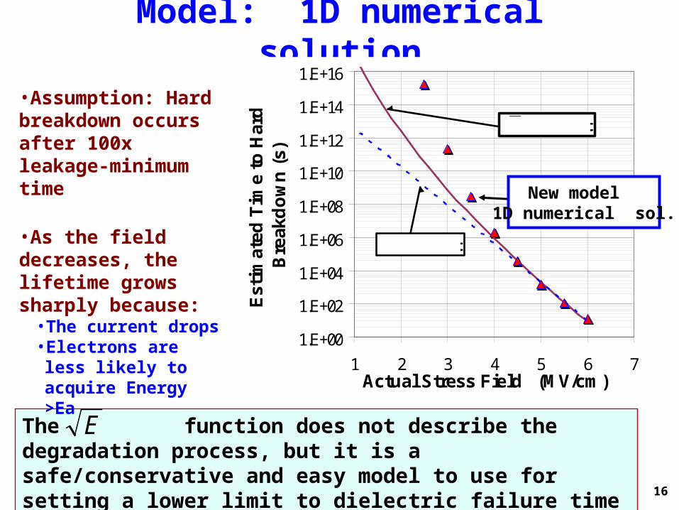
Model: 1D numerical solution
The function does not describe the degradation process, but it is a safe/conservative and easy model to use for setting a lower limit to dielectric failure time vs. Field.
•Assumption: Hard breakdown occurs after 100x leakage-minimum time
•As the field decreases, the lifetime grows sharply because:
• The current drops • Electrons are less likely to acquire Energy >Ea
E
1.E+00
1.E+02
1.E+04
1.E+06
1.E+08
1.E+10
1.E+12
1.E+14
1.E+16
1 2 3 4 5 6 7Actual Stress Field (MV/cm)
Est
imat
ed T
ime
to H
ard
B
reak
do
wn
(s)
E -model fit
√E -model fit
New model 1D numerical sol.

17
Model: 1D numerical solution
The parameters used to fit the model to the observed data are physical:
•The apparent acceleration factor at test fields is 5.3 cm/MV (a 1D model assumes that A does not vary with E)
•The apparent activation energy at test fields is 0.1 – 0.2 eV
eVeVEeVE Btrapa 7.1;7.0;4.2
;105.1;103,0 837 cmcmxttrap
12.0;6.2;5.0 pkmm eeff
1
10
100
15 25 35 45
1/kbT (1/eV)E
st.
Tim
e t
o H
ard
B
rea
kd
ow
n
(s)
-slope = E a = 0.16 eVat 5 MV/cm
=Ea,App =

18
Model SummaryA simple model for low-k dielectric degradation is suggested: •Electrons accelerate in the field between collisions with traps. •The energy acquired by the electrons generates new traps. •Electrons are allowed to either leave the traps thermally or tunnel
between traps
The Model agrees with experimental observations:
•Initial trap buildup lowers conductivity due to enhanced scattering.•At typical test stress conditions, the trap density increases very
quickly (before a first current-measurement is completed) and then the growth slows down substantially.
•Additional trap-density-increase less than x10 brings the trap density to a value where leakage starts rising.
•The same trap density that causes the onset of leakage-increase under high voltage would not yet show any leakage-increase at low voltage.
•The electrons “heat up” due to the energy gained at high E-field (accelerated test): The wafer temperature effect is small (low apparent activation energy).

19
Conclusions
•Trap creation requires charge flux, and hence, a local degradation would be self-accelerated.
•At a later stage, trap creation is self inhibited, due to insufficient mean free path for the carriers to acquire enough energy in the electric field.
•The lifetime at operating voltages, where the E-field X mean-free-path drops below the activation energy for rearranging atoms to form traps, becomes extremely long in respect to the E-model prediction.
•Although not describing the process, the √E-model is easy to use, and sets a safe conservative lower-limit to lifetime predictions.