IRPS2005 P5 A 1
18
Gaddi S. Haase Gaddi S. Haase , Ennis T. Ogawa , Ennis T. Ogawa And Joe W. McPherson And Joe W. McPherson SiTD, Texas Instruments, Inc. Dallas, TX, USA T EXAS I NSTRUM ENTS Breakdown Characteristics of Interconnect Dielectrics 5A.1
-
Upload
guest3b6d2b -
Category
Economy & Finance
-
view
361 -
download
1
Transcript of IRPS2005 P5 A 1

Gaddi S. HaaseGaddi S. Haase, Ennis T. Ogawa, Ennis T. OgawaAnd Joe W. McPhersonAnd Joe W. McPherson
SiTD, Texas Instruments, Inc.Dallas, TX, USA
TEXAS INSTRUMENTS
Breakdown Characteristics of
Interconnect Dielectrics
5A.1

2
• Characterize interconnect dielectric breakdown:– Low-k dielectrics and interfaces have low dielectric strength– Line-to-line spacing < 100nm – Line length (@ min. pitch) generally > 100m
• Develop a method to distinguish benign CD/profile variation effects from actual material defectivity– Unlike gate oxide thickness, CMP/litho/etch during BEOL
processing introduce significant variations
Purpose

3
• A basic model for dielectric breakdown
• Line-to-line spacing variations effects
• A dual V-ramp-rate methodology
• Experiment details
• Results
• Extracting breakdown parameters
• Comparison to TDDB
• Discussion
• Conclusions
Outline

4
• The E-model for dielectric breakdown (A. Berman; J.W. McPherson):
– H*0 = zero-field activation energy– = the field acceleration parameter
• A constant field TDDB measurement can be replaced by a voltage ramp to breakdown (A. Berman):
– t0 is the effective lifetime at Ebd
– E and are the ramp step parameters
Introduction
ETko
Tk
Ep
obd eeAeAt b
o
b
effo
**
E
EEn
n
EEn
eet
BD
BD
10
)(0

5
• We need to work in V space:– V is the stress voltage– s is the (minimum) line-to-line
spacing within a test structure, where the breakdown actually occurred. V
se
t
10
)(
0)(VV
sbd
bd
etVt
0.3
0.4
0.5
0.6
0.7
0.8
0.9
1
70 90 110 130 150 170 190Minimum Line-to-Line spacing (nm),
at the top of the lines
Re
lati
ve
Ele
ctr
ic F
ield
(Arb
. U
nit
s)
90 nmnode
130 nmnode
Line-to-line spacing (nm)
The sensitivity of E-field uncertainty to spacing variations

6
• Ramping V at two ramp rates, with same V but different and:
The dual ramp-rate (2RR) methodology:
• If we know , we know the min. spacing si where the breakdown occurred
• The index i represents an individual DUT.– Unfortunately, we cannot
break the same test structure twice.
– Instead, use well mixed, large sister populations of test structures
iRViRVs bdbdi ,,ln 12
1
2
1
Breakdown
spacing
-5
-4
-3
-2
-1
0
1
2
3
20 22 24 26 28 30 32 34 36 38 40
Breakdown voltage (V)
ln[-
ln(1
-F)]
0.2V/1770ms step
0.2V/170ms step
Linear(0.2V/1770ms step)Linear (0.2V/170msstep)
Example: 50nm thick, homogenous SiNx film

7
Spacing distribution at the top of the metal lines, from FIB-SEM cross-sections
00.10.20.30.40.50.60.70.80.9
1
80.00 90.00 100.00 110.00 120.00 130.00
Line-to-line spacing (nm) at the top of the line
Cu
m.
Pro
b.
M2
M1
b
Experimental details: The test structure
Serpent
Lower Comb
Upper Comb
Nominal Linewidth, 0.14 m
Nominal Line-to-
Line Spacing, 0.13 m
ILD = IMD = Orgno-Silicate Glass (OSG)
ESL = SiCxNy
Line-to-line spacing in a single test structure (DUT)
a
CuM1level
IMDESL ILD
8
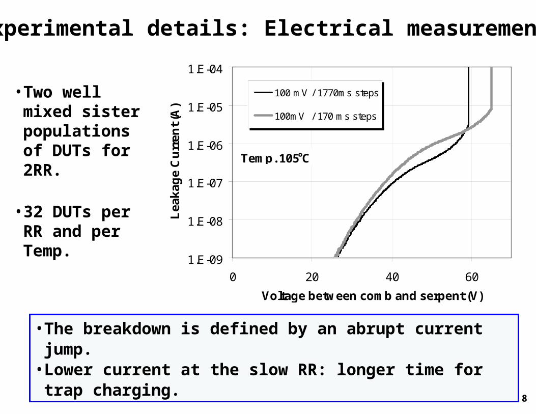
Experimental details: Electrical measurement
• Two well mixed sister populations of DUTs for 2RR.
• 32 DUTs per RR and per Temp.
• The breakdown is defined by an abrupt current jump.• Lower current at the slow RR: longer time for trap charging.
1.E-09
1.E-08
1.E-07
1.E-06
1.E-05
1.E-04
0 20 40 60
Voltage between comb and serpent (V)
Le
ak
ag
e C
urr
en
t (A
)
100 mV / 1770ms steps
100mV / 170 ms steps
Temp. 105 C°

9
– Linear fit/smooth to Weibull plot
– Data sorted by Vbd
– =4.1 cm/MV to fit si dist.
– Polynomial fit/smooth
Breakdown test results : Data for 23°C
0
0.2
0.4
0.6
0.8
1
50 55 60 65 70 75Vbd (V)
F =
Cu
m.
Pro
b. 0.1 V/1.77s
0.1 V/0.17s
Poly. (0.1V/1.77s )Poly. (0.1V/0.17s )
23 C°
-5-4-3-2-1012
50 55 60 65 70 75Vbd (V)
Ln
[-L
n(1
-F)]
0.1 V/1.77s
0.1 V/0.17s
Line_slow
Line_fast
Linear(Line_slow)Linear(Line_fast)
23 C°
0
0.2
0.4
0.6
0.8
1
0.07 0.08 0.09 0.1 0.11 0.12Min. Spacing (m) for =4.1 cm/MV
F =
Cu
m.
Pro
bab
ilit
y 2nd order fit of F
linear fit to ln[-ln(1-F)]
23 C°
iRViRVs bdbdi ,,ln 12
1
2
1

10
0
0.2
0.4
0.6
0.8
1
0.07 0.08 0.09 0.1 0.11 0.12Min. Spacing (m) for =3.94 cm/MV
F =
Cu
m.
Pro
bab
ilit
y 2nd order fit to F
linear fit to ln[-ln(1-F)]
250 C°
iRViRVs bdbdi ,,ln 12
1
2
1
• Correlation between Vbd and min. line-to-line spacing per DUT.
0
0.2
0.4
0.6
0.8
1
45 50 55 60 65 70Vbd (V)
F =
Cu
m.
Pro
b. 0.1 V/1.77s
0.1 V/0.17s
line_fast
line slow
Poly. (lineslow)Poly.(line_fast)
250 C°
-5-4-3-2-1012
45 50 55 60 65 70Vbd (V)
Ln
[-L
n(1
-F)]
0.1 V/1.77s
0.1 V/0.17s
Line_slow
Line_fast
Linear(Line_slow)Linear(Line_fast)
250 C°
Breakdown test results: Data for 250°C
• Note: i can be replaced by F ONLY if Vbd is a monotonic function of si

11
Temperature effect on breakdown parameters
• 2RR-extracted : – shows little or no
dependence on T– = 4.1±0.2 cm/MV
• Ebd=Vbd(F=63%)/si(F=63%)
– Low zero-field activation energy
– H*0= 0.14±0.02 eV
2
3
4
5
6
20 25 30 35 40
1/kbT (1/eV)
(c
m/M
V)
Experiment
1/T, based on 4.5 cm/MV@ 105CLinear (Experiment)
4
5
6
7
8
20 25 30 35 401/kbT (1/eV)
Eb
d (
MV
/cm
)
si(F=63%)=100nm

12
Comparison to constant-voltage TDDB tests at three temperatures
• Well mixed site locations • Avoided wafer edges
T = 24°C
-5
-4
-3
-2
-1
0
1
2
0.1 1 10 100 1000 10000Time to breakdown (s)
Ln
(-L
n(1
-F))
66.0 V
60.5 V
55 V
Log. (66.0V )Log. (60.5V )Log. (55V )
T = 105°C
-5
-4
-3
-2
-1
0
1
2
0.1 1 10 100 1000 10000Time to breakdown (s)
Ln
(-L
n(1
-F))
66.0 V
60.5 V
49.5 V
Log. (66.0V )Log. (60.5V )Log. (49.5V )
T = 250°C
-5
-4
-3
-2
-1
0
1
2
0.1 1 10 100 1000 10000Time to breakdown (s)
Ln
(-L
n(1
-F))
60.5 V
55.0 V
49.5 V
Log. (60.5V )Log. (55.0V )Log. (49.5V )

13
Comparison to constant-voltage TDDB
si(F=63%)=100nm
3
3.5
4
4.5
5
5.5
6
20 25 30 35 40 45
1/(kbT) (1/eV)
(c
m/M
V)
1
10
100
1000
10000
10 20 30 40 50
1/(kbT) (1/eV)
t bd(F
=6
3%
)
(s
)
6.05 MV/cm
5.5 MV/cm
Expon. ( 6.05MV/cm )Expon. ( 5.5 MV/cm )
TDDB @ F=63% :
• Again: little/no temperature
dependence for = 4.25±0.05 cm/MV
• Again: low zero-field activation enthalpy
H*0= 0.16±0.01 eV

14
Summary of experimental data
• Good agreement between 2RR V-ramp to breakdown and constant voltage TDDB tests: Consistent with E-model for the range of E-fields used.
• V-ramp to breakdown is faster than TDDB.
• For the wafers tested: Vbd (or lifetime) distribution is predominantly impacted by the distribution of the “minimum” line-to-line spacing per DUT.
• Ebd values can be corrected for true spacing.

15
Example for Defect Detection
-5-4-3-2-10123
0 20 40 60 80 100
Breakdown voltage (Volts)
ln[-
ln(1
-F)]
Fast (0.2 V/ 170 ms)Slow (0.2 V/ 1770 ms)
When for low Vbd events, does NOT decrease monotonically with decreasing Vbd.
iRViRV bdbd ,, 12

16
Discussion• The low apparent zero-field activation enthalpy H*0 and
the substrate temperature independent field acceleration parameter suggest:
• Note: Not every BEOL integration scheme will be expected to show the same behavior.
Several competing dielectric degradation channels
A leakage-current model, where the charge carriers do not thermalize with the substrate.
Cu Cu
SiCxNy
O H
O H
O-Si--C-H
e- en
ergy

17
Conclusions
• Line-to-line spacing variations can not be ignored.
• 2RR V-ramp to breakdown methodology allows us to:
– Map a whole wafer relatively rapidly.
– Determine if the spread in the Vbd distribution is dominated by
variations in the DUTs’ min. spacing.
– Separate low Vbd cases that are dominated by defects.
– Obtain a corrected Ebd distribution (using the true minimum
spacing) - only if Vbd is well correlated with spacing.
– Extract activation energy and field-acceleration parameters:
• In this study: Little/no temperature dependence for
• In this study: Low apparent zero-field activation energy.
• 2RR V-ramp to breakdown cannot replace low field TDDB

18
Acknowledgements
• Eden Zielinski
• Ting Tsui
• Mona Eissa
• Ralf Willecke
• Bill Dostalik
• Yong Choi
• Andrew McKerrow
• Honglin Guo
• Jinyoung Kim
• Homi Mogul