Objectives Accessing and Navigating within AQS Resources available on the AQS Website AQS Support.

IPSO 19" & IPSO AQS
AVANCE IIIUser Manual
Version
001
The information in this manual may be altered without notice.
BRUKER BIOSPIN accepts no responsibility for actions takenas a result of use of this manual. BRUKER BIOSPIN acceptsno liability for any mistakes contained in the manual, leading tocoincidental damage, whether during installation or operation ofthe instrument. Unauthorized reproduction of manual contents,without written permission from the publishers, or translationinto another language, either in full or in part, is forbidden.
This manual was written by
Dr. Jens Rommel
© April 27, 2007: Bruker Biospin GmbH
Rheinstetten, Germany
P/N: Z31819DWG-Nr.: Z4D10351 - Version 001

IPSO AQS
IPSO 19”
IPSO Manual
1
BRUKER BioSpin Computer/Hardware Manual
2007–04–27
Intelligent Pulse Sequenz Organizer (IPSO)This Manual covers the spectrometer control unit called IPSO as version
� IPSO 19”
� IPSO AQS
which are used in the AVANCE III spectrometers
Chapter “1.” summarizes the most essential informations for users to get started quickly and toavoid beginner’s mistakes without reading plenty of pages.
Chapter “2.” lists the part/order numbers of the main assemblies, subassemblies and devices.
Chapter “3.” et seqq. provide the more detailed descriptions of assemblies and devices.
1. Condensed Introduction
Do’s and Don’ts
� Do not connect a receiver to the LVDS connector of the controller inSlot2 of the IPSO 19” Unit. There will never be valid data.
� A LVDS cable should never be removed from or connected to a poweredcontroller. Corrupted data could be sampled as valid.
� Do not connect more than one Gradient Amplifiers to the same system.
1. 1. Structure and Features
Features
� IPSO is a digital spectrometer control unit with a variable number of out-put channels (Tx–Controllers)
� Each Tx–Controller outputs a stream of 48–bit words at a clock rate of 80MHz per word
� Transferral of a complete set of frequency parameters requires two words.
� The time resolution of parameter switching in any combination of Fre-quency, Phase, Amplitude is 12.5 nsec.
� The minimal duration of any combination of parameters is 25 nsec.
� Gradient channels require one word per gradient.
� The maximal number of addresses for different gradients (the max. num-ber of gradient channels) is 1k.
� A constant time delay between the outputs of the different Tx–Controllersmay be adjusted to any number of 80MHz clock cycles up to229x12.5nsec
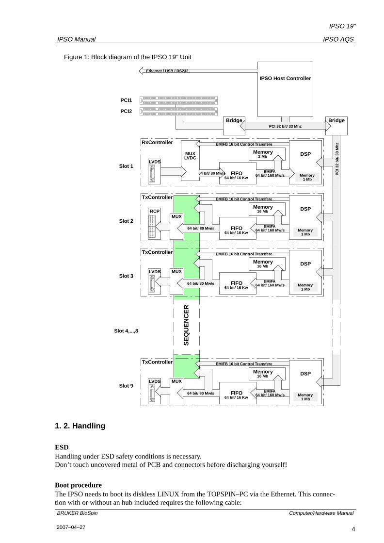
StructureThe distinctive Parts of the system are the Host Controller charged with administrative tasks, thenumber of Tx–Controllers generating and transferring the parameter sequences and the Sequencerproviding for a means of communication between the Tx–Controllers.

IPSO AQS
IPSO 19”
IPSO Manual
2
BRUKER BioSpin Computer/Hardware Manual
2007–04–27
The ControllersThe system contains the 3 types of controllers, Host Controller, Rx–Controller and the Tx–Con-troller.
Host Controller: There is only one Host Controller in the system. The Host Controlleris an IBM compatible PC with all standard interfaces thus making ac-cess possible to the whole pool of standard hardware and software.
The Host Controller boots its operating system software (diskless LI-NUX) from and communicates with the TOPSPIN–PC over Ethernet.It also communicates over its standard interfaces with the Rx– and theTx–Controllers and with peripheral devices.
Rx–Controller: The Rx–Controller is able to receive 48–bit words at its LVDS inter-face at a rate of up to 100–Mega words. Therefore it can be used as afast data link from the receiver channel to the transmit channel, by-passing the ethernet and the TOPSPIN–PC. Furthermore all Tx–Con-trollers and their LVDS interfaces can be tested with the IPSOTEST iftheir interfaces are connected to a Rx–Controller.
Realtime processing of that data can be done by an onboard DSP. Theprocessed data can be transferred by the DMA channels of the DSPover the system bus to any other controller or may be fetched by anyother controller.
Usually there is one Rx–Controller in the system. Without additionalsoftware (that means transparent to the software) it is possible to in-clude additional Rx–Controllers using extension boxes.
The Rx–Controller has no connections to the Sequencer and commu-nicates and exchanges data with other controllers via the system bus.It will function in any slot of the IPSO but should be inserted in slot 1.
Tx–Controller: Depending on its configuration, the Tx–Controller can be used for anyof the 3 output functions in the system. These functions are the T–Controller servicing the RCP outputs at T0 with timing signals, theF–Controller generating the frequency parameters for the SGUs andthe G–Controller generating the gradient packets for the amplifiers.
The Tx–Controllers and their common Sequencer are the most deci-sive parts of the IPSO system. The Sequencer is a single device, justone piece of silicon. It contains the communication and decision mak-ing logic of all Tx–Controllers and the communication bus betweenthem known from former systems as the AQ–Bus. The AQ–Bus al-lows for real time communication on a 1–clock base of 12.5 nsec.
The controller itself consists of a DSP with memory, FIFO, outputlogic and interfaces to the system bus and the Sequencer. The DSPgets its code from the Host Controller, generates the parameter se-quences and writes them into the FIFO. Its most important task is tokeep the FIFO full. The Sequencer (once started) reads the words outof the FIFOs of all controllers, realizes the defined timing in eachchannel and controls the outputs.
The global functions of the Sequencer (e.g. START, STOP, SUS-PEND, RESUME and so on) are part of the Sequencer logic of theT–Controller. Therefore a T–Controller has to be in the system tocarry out any type of acquisition.

IPSO AQS
IPSO 19”
IPSO Manual
3
BRUKER BioSpin Computer/Hardware Manual
2007–04–27
LVDSThe LVDS cable is the transport media for digital data words between the Tx– and the Rx–Con-trollers respectively and the peripheral devices like SGU, Gradient Amplifier, DRU and DPP(Digital Preemphasis Processor). The abbreviation LVDS means “low voltage digital signal”.The voltage switching range of the data lines is between 1.0V and 1.4V.
The used devices take 48–bit data words at a clock rate of 80MHz (and 100MHz between DRUand Rx–Controller respectively) and serialize and transport them over 8 balanced data line pairsaccompanied by one clock pair. At the receiver side the data stream is deserialized and the48–bit data word and its 80MHz clock are reconstructed.
Because there are 8 data lines, the cable has to transport 6 data bit plus one balance bit per12,5nsec. That means a bit frequency of 560MHz on each data line. Since a good signal qualityneeds a good transmission behavior up to the fifth harmonic wave this cable has to transport thesignals up to about 3–GHz without frequency dependent distortions.
The LVDS cable driver is always active even if the Tx–Controller is transmitting no valid data.
There are 2 options called “Deskew” and “Preemphasis” which are intended to compensate thenegative influence of cables longer than about 3 meters to the signal quality. The usual cablelength below 2 meters requires neither Deskew nor Preemphasis.
Deskew: This feature minimizes the effective skew of the different data linepairs in the cable. To be effective it has to be enabled at the receiverand carried out at the transmitter. The default state at introduction is“NOT ENABLED” at the receiver and is activated at the transmitterby a software command only.
If enabled at the receiver Deskew has to be carried out after power–upand again each time after the cable has been plugged out and in underpower. This can be done by software using the command “Deskew” ofthe “ipsotest ” program.Software activated Deskew needs TOPSPIN 2.0b6 and a Tx–Control-ler with Part# “H12538F2”. Otherwise with “Deskew enabled at thereceiver” the system has to be powered up again after reconnecting.
Preemphasis: This feature compensates for the greater need of charge on cables lon-ger than 2 meters. To be effective it needs one cable–length–depen-dent resistor at the transmitter. If ever necessary such Tx_Controllerswill be given a special part number.
The state of the Tx–Controllers with part number “H15538” and”H15538F1” and H12538F2 is “NO PREEMPHASIS”
Besides the data and clock lines the LVDS cable includes 4 lines of an USB channel (unused sofar) and 2 state lines. The state lines tell the Tx–Controller the kind of the connected device like“unconnected, SGU connected, Gradient Amplifier connected, DPP connected”.
IPSO AQS
IPSO 19”
IPSO Manual
4
BRUKER BioSpin Computer/Hardware Manual
2007–04–27
Figure 1: Block diagram of the IPSO 19” Unit
FIFO64 bit/ 16 Kw
MUX
FIFO64 bit/ 16 Kw
Memory16 Mb
1 MbMemory
DSP
EMIFA 64 bit/ 160 Mw/s
EMIFB 16 bit Control Transfere
LVDS
TxController
MUX
FIFO64 bit/ 16 Kw
Memory16 Mb
1 MbMemory
DSP
EMIFA 64 bit/ 160 Mw/s
EMIFB 16 bit Control Transfere
RCP
TxController
MUX
FIFO64 bit/ 16 Kw
Memory2 Mb
1 MbMemory
DSP
EMIFA 64 bit/ 160 Mw/s
EMIFB 16 bit Control Transfere
LVDS
RxController
64 bit/ 80 Mw/s
64 bit/ 80 Mw/s
64 bit/ 80 Mw/s
LVDC
MUX
Memory16 Mb
1 MbMemory
DSP
EMIFB 16 bit Control Transfere
LVDS
TxController
64 bit/ 80 Mw/s
SE
QU
EN
CE
R
EMIFA 64 bit/ 160 Mw/s
BridgeBridgePCI 32 bit/ 33 Mhz
IPSO Host Controller
Ethernet / USB / RS232
PCI1
PCI2
Slot 1
Slot 2
Slot 3
Slot 4,...,8
Slot 9
PC
I 32
bit/
33 M
hz
1. 2. Handling
ESDHandling under ESD safety conditions is necessary. Don’t touch uncovered metal of PCB and connectors before discharging yourself!
Boot procedureThe IPSO needs to boot its diskless LINUX from the TOPSPIN–PC via the Ethernet. This connec-tion with or without an hub included requires the following cable:
IPSO AQS
IPSO 19”
IPSO Manual
5
BRUKER BioSpin Computer/Hardware Manual
2007–04–27
Connection Type Color Part# Length
point to point UTP/CAT5 crossed red84338 5m
point–to–point UTP/CAT5, crossed red83980 10m
point to h b UTP/CAT5 straight hite83025 5m
point–to–hub UTP/CAT5, straight white83026 10m
If connected, the IPSO needs only to be switched on or to be resetted to begin booting.
Power ON/OFF ButtonTo be effective this button needs to be pressed for about 2 seconds to switch the system on and 6seconds to switch it off.
Reset ButtonThis button resets the Host Controller, the PCI logic and restarts the boot process. So it leads tothe same result as ON/OFF without Power OFF.
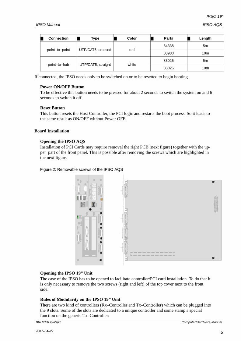
Board Installation
Opening the IPSO AQSInstallation of PCI Cards may require removal the right PCB (next figure) together with the up-per part of the front panel. This is possible after removing the screws which are highlighted inthe next figure.
Figure 2: Removable screws of the IPSO AQS
ÉÉ
É
ÏÏÏÏÏÏÏÏÏÏÏÏÏÏÏ
ÉÉ
ÉÉ
ÉÉ
ÉÉ
ÎÎÎÎÎÎ
ÉÉÉÉ
ÉÉ
ÉÉ
Opening the IPSO 19” UnitThe case of the IPSO has to be opened to facilitate controller/PCI card installation. To do that itis only necessary to remove the two screws (right and left) of the top cover next to the frontside.
Rules of Modularity on the IPSO 19” UnitThere are two kind of controllers (Rx–Controller and Tx–Controller) which can be plugged intothe 9 slots. Some of the slots are dedicated to a unique controller and some stamp a specialfunction on the generic Tx–Controller:
IPSO AQS
IPSO 19”
IPSO Manual
6
BRUKER BioSpin Computer/Hardware Manual
2007–04–27
Rx–Controller: Slot1 is intended to be used by the Rx–Controller only. But it wouldwork as receiving controller in any other slot.
Tx–Controller: Slot2 to Slot9 are designed to be Tx–Controller’s places. Plugged intoSlot1 the Tx–Controller would be recognized as “unknown” (U–Con-troller) but it will not be able to communicate with the sequencer andto transmit data.
Slot2: Only this slot provides access to the acquisition global functions likeSTART, STOP and so on and to the RCP outputs. Therefore the Tx–Controller in this slot gets the task of the T–Controller. It controls theRCP outputs instead of its LVDS output. Do not connect a cable tothis LVDS connector. The LED below this connector is always off.
Slot3 to Slot9: Tx–Controllers in these slots can work as F–Controller (default) orG–Controller.
The LED below the LVDS connector lights green at the F–Controllerand yellow at the G–Controller.
The channel numbering of the F–Controller begins at the leftmost oneand counts up to the right. There must not be any gap between theF–Controllers.
Which F–Controller will become the G–Controller?Only the F–Controller which is connected to a Gradient Amplifier will be configured as G–Con-troller and its LED below the LVDS connector will change from green to yellow.
Connecting more than one Controller to a Gradient Amplifier is not supported by TOPSPIN.
Previous to Rel.2.0, TOPSPIN will only allow the last F–Controller of a system to become theG–Controller. This would be the last one at the right side on “IPSO 19” Unit” and F/G–Control-ler–4 on “IPSO AQS”.
A later release might advantageously allow the G–Controller to be freely selected by connectingthe Gradient Amplifier.
Until then an arbitrary F–Controller can be selected as G–Controller if all higher numbered F–Controllers will be logically disabled.
For Example:You use 3 F–Controllers and 1 G–Controller which is in the slot of FxController–4.If you want to disable the present G–Controller and use FxController–3 instead, you have to
1. unplug the LVDS–Cable from previous G–Controller
2. plug the LVDS–Cable to FxController–3
3. login to IPSO as root
4. and run root@IPSO:/opt/test> sh aqmod.sh –disable fctrl4 ↵
1. 3. Ports
The IPSO services the following Input– and Output Ports

21 5
6 9
IPSO AQS
IPSO 19”
IPSO Manual
7
BRUKER BioSpin Computer/Hardware Manual
2007–04–27
Figure 3: Front View of IPSO 19” Unit
tty4 tty5
Figure 4: Front View of IPSO AQS
ÉÉÉÉ
ÉÉÉÉÉÉ
ÉÉÉÉÉÉ
ÎÎÎÎÎÎÎÎÎÎÎÎÎÎÎÎÎÎÎÎÎÎÎÎ
ÉÉÉÉ
ÉÉÉÉ
ÉÉÉÉÉÉ
tty4 tty5
IN OU
T
PCI SlotsThe two standard PCI slots meet the “PCI Local Bus Specification, Rev.2.1”. Both slots are in-tended for 5–Volt signaling cards (IPSO AQS can accept short cards only).
The total power consumption, summarized for both slots, must not exceed the following values:
IPSO 19” Unit: 10A from +5V and 3.5A from 3.3V
IPSO AQS: 10A from +5V and 5A from 3.3V
Connectors
tty0, tty1: RS232C on ETX module, max. baud rate 115.2KbaudThe configuration of the tty–interfaces (parity, number of stop bits,kind of handshake, baud rate) is defined and set by the applicationprogram.
Type of connector is D–Sub, 9 pin, female
Pin # Signal Pin # Signal Pin # Signal1 RI 4 DTR 7 RTS2 RxD 5 GND 8 CTS3 TxD 6 DSR 9 not con.
tty4, tty5: RS232C on auxiliary PCI adapter EX–41052, max. baud rate 115.2KbaudThe configuration of the tty–interfaces (parity, number of stop bits,kind of handshake, baud rate) is defined and set by the applicationprogram.
21 5
6 9
IPSO AQS
IPSO 19”
IPSO Manual
8
BRUKER BioSpin Computer/Hardware Manual
2007–04–27
Type of connector is D–Sub, 9 pin, female
Pin # Signal Pin # Signal Pin # Signal1 CDC 4 DTR 7 RTS2 RxD 5 GND 8 CTS3 TxD 6 DSR 9 RI
ETH 10/100 BaseT, Intel 82551ER
USB USB 1.1 OHCI
The Real Time Pulses (RCP) on Connector T0
Electrical Properties and Constraints of the RCP outputs and receiver inputsThe high and low switching levels (U2) and the associated current (Ic) of the RCP signals de-pend on the circuitry and driving capacity of the driver and the circuitry of the connected re-ceiver.
Figure 5: RCP Circuit
R2
R14,7k
RS
10
U2UC
IC_low
IC_high
IPSO RCP OutReceiver RCP InVcc Vcc
U2_low�high �VCC �UC_low�high �
R1RS
1� R1R2�
R1RS
IC_low�high �U2_low�high �UC_low�high
RS
VCC � 5V
UC_low � 0, 3V
UC_high � (3, 0���3, 3)V
The table shows the resulting voltage levels and currents for some combinations of R1/R2. Othercombinations are possible and can be checked by the formulas above.
Table 1: RCP voltage levels and currents
Parameter Combinations of Input Circuit Units
R1 100 100 100 200 Ohm
R2 68 � 100 200 Ohm
U2 if IC=0 2,0 5,0 2,5 2,5 V
U2_low 0,64 0,73 0,66 0,5 V
U2_high 2,8 3,18 2,91 2,95 V

IPSO AQS
IPSO 19”
IPSO Manual
9
BRUKER BioSpin Computer/Hardware Manual
2007–04–27
Parameter UnitsCombinations of Input Circuit
Ic_low 34 43 36 20 mA
Ic_high –20 –12 –30 –25 mA
Signals and Location
IPSO 19” UnitThe signals which are available at the front side connector T0 are:
Type of Signal Direct. Name Count
RCP Output out TCU_xy 51
Trigger Input in Trig 1,...,4 4
Extern Suspend in EXT_MAN_SUSP 1
Extern Stop in EXT_MAN_STOP 1
Emergency Stop in/out EX_SGU_RES 1
Peripheral Status in SGU_ST 1
Next Value Clock for Preemphasis out EXT_GCLK 1
Another 19 RCP signals (shown in red in column “T0”) are available at connector ST47 insideof the IPSO case.
Figure 6: RCP pin location of IPSO 19” Unit
1 3 5
2 4 6
1 3 5
2 4 6
1 3 5
2 4 6
1 3 5
2 4 6
1 3 5
2 4 6
1 3 5
2 4 6
1 3 5
2 4 6
1 3 5
2 4 6
1 3 5
2 4 6
1 3 5
2 4 6
1 3 5
2 4 6
T0
Z A B C D E F G H I
Table 2: Pin assignment of the RCP signals on IPSO 19” Unit
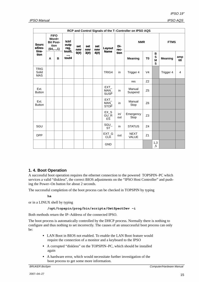
RCP and Control Signals of the T–Controller on IPSO 19” Unit
Source/Destina-
tion
FIFOWord+ BitPosition(64,...,1)
tctrloutput
reg.tout0,
setnmr0(#)
setnmr3(#)
setnmr4(#)
LayoutName
Di-rec-tion
NMR
tionA B
tout0 ,...,
tout4
0(#) 3(#) 4(#) Name tionMeaning T0 BS
MS
BSMS/LCB 2 T0(0) 0 TCU62 out !LOCK_HOLD B1 2
BSMS/SCBR 3 T0(1) 1 TCU0 out !HOMOSPOIL B2 6
1HTransm. 4 T0(2) 2 TCU1 out SELH_!H/F B4
1HTransm. 5 T0(3) 3 TCU2 out SELX_!X/F B5
BSMS/LCB 6 T0(4) 4 TCU3 out !INT_A_(Z0) B3 4
BP 7 T0(5) 5 TCU4 out MIXCC B6

IPSO AQS
IPSO 19”
IPSO Manual
10
BRUKER BioSpin Computer/Hardware Manual
2007–04–27
RCP and Control Signals of the T–Controller on IPSO 19” Unit
Source/Destina-
tion
NMRDi-rec-tion
LayoutName
setnmr4(#)
setnmr3(#)
setnmr0(#)
tctrloutput
reg.tout0,
...,tout4
FIFOWord+ BitPosition(64,...,1)
Source/Destina-
tionBSMST0Meaning
Di-rec-tion
LayoutName
setnmr4(#)
setnmr3(#)
setnmr0(#)
tctrloutput
reg.tout0,
...,tout4BA
8 T0(6) 6 TCU5 out res C1
HPPR 9 T0(7) 7 TCU6 out RCP_PA_SWITCH C2
QNP 10 T0(8) 8 TCU7 out FXA C3
QNP 11 T0(9) 9 TCU8 out FXB C4
12 T0(10) 10 TCU9 out res D1
13 T0(11) 11 TCU10 out res D2
14 T0(12) 12 TCU11 out res D3
15 T0(13) 13 TCU12 out res D4
16 T0(14) 14 TCU13 out res D5
17 T0(15) 15 TCU14 out res D6
18 T1(0) 16 TCU15 out res G1
19 T1(1) 17 TCU16 out res G2
20 T1(2) 18 TCU17 out res G3
21 T1(3) 19 TCU18 out res G4
22 T1(4) 20 TCU19 out res G5
23 T1(5) 21 TCU20 out res G6
24 T1(6) 22 TCU21 out res H1
25 T1(7) 23 TCU22 out res H2
MED 26 T1(8) 24 TCU23 out ECG_START_TRIG H3
MED 27 T1(9) 25 TCU24 out AUT_TUNG_IN H4
MED 28 T1(10) 26 TCU25 outAK-
TIV_DEC_RES
H5
MED 29 T1(11) 27 TCU26 outAK-
TIV_DEC_RES
H6
MED 30 T1(12) 28 TCU27 out Customerspecified I1
MED 31 T1(13) 29 TCU28 out Customerspecified I2
MED 32 T1(14) 30 TCU29 out Customerspecified I3
MED 33 T1(15) 31 TCU30 out Customerspecified I4
34 T2(0) 0 TCU31 out GAIN_0_TR1
35 T2(1) 1 TCU32 out GAIN_1_TR1
IPSO AQS
IPSO 19”
IPSO Manual
11
BRUKER BioSpin Computer/Hardware Manual
2007–04–27
RCP and Control Signals of the T–Controller on IPSO 19” Unit
Source/Destina-
tion
NMRDi-rec-tion
LayoutName
setnmr4(#)
setnmr3(#)
setnmr0(#)
tctrloutput
reg.tout0,
...,tout4
FIFOWord+ BitPosition(64,...,1)
Source/Destina-
tionBSMST0Meaning
Di-rec-tion
LayoutName
setnmr4(#)
setnmr3(#)
setnmr0(#)
tctrloutput
reg.tout0,
...,tout4BA
36 T2(2) 2 TCU33 out C/AB_TR1
37 T2(3) 3 TCU34 out GAIN_0_TR2
38 T2(4) 4 TCU35 out GAIN_1_TR2
39 T2(5) 5 TCU36 out GAIN_2_TR2
40 T2(6) 6 TCU37 outGAIN_2_TR
1
1H1 KWAMPL 41 T2(7) 7 TCU38 out RELAY_H E3
X1 KWAMPL 42 T2(8) 8 TCU39 out RELAY_X E4
X1 KWAMPL 43 T2(9) 9 TCU40 out RELAY_Y E5
44 T2(10) 10 TCU41 outres
RACK_ON/OFF
E6
45 T2(11) 11 TCU42 out RCP F1
X1 KWAMPL 46 T2(12) 12 TCU43 out RELAY Z F2
47 T2(13) 13 TCU44 out RCP_Scope F3
48 T2(14) 14 TCU45 out RCP_EXT_DEV F4
49 T2(15) 15 TCU46 out RCP F5
HIGHPOWE
R50 T3(0) 16 TCU47 out STP1_DIR
HIGHPOWE
R51 T3(1) 17 TCU48 out LB_SEL
HIGHPOWE
R52 T3(2) 18 TCU49 out DCM_STRT
HIGHPOWE
R53 T3(3) 19 TCU50 out STP1_CLK
HIGHPOWE
R54 T3(4) 20 TCU51 out STP2_CLK

IPSO AQS
IPSO 19”
IPSO Manual
12
BRUKER BioSpin Computer/Hardware Manual
2007–04–27
RCP and Control Signals of the T–Controller on IPSO 19” Unit
Source/Destina-
tion
NMRDi-rec-tion
LayoutName
setnmr4(#)
setnmr3(#)
setnmr0(#)
tctrloutput
reg.tout0,
...,tout4
FIFOWord+ BitPosition(64,...,1)
Source/Destina-
tionBSMST0Meaning
Di-rec-tion
LayoutName
setnmr4(#)
setnmr3(#)
setnmr0(#)
tctrloutput
reg.tout0,
...,tout4BA
HIGHPOWE
R55 T3(5) 21 TCU52 out RES_STP1
HIGHPOWE
R56 T3(6) 22 TCU53 out DCM_RES
HIGHPOWE
R57 T3(7) 23 TCU54 out GO_POS
2H LockSwitch 58 T3(8) 24 TCU55 out SEL_2H AMP A1
59 T3(9) 25 TCU66 out res
60 T3(10) 26 TCU57 out res Z2
61 T3(11) 27 TCU58 out Q_SWITCH A3
2H LockSwitch 62 T3(12) 28 TCU59 out SEL_!X/2H A2
63 T3(13) 29 TCU60 out res F6
64 T3(14) 30 TCU61 out res I5
58 T3(15) 31 TCU56 out res I6
GRASP 59 T4(0) 32 TCU63 out BLK_GRAD_X A4
GRASP 60 T4(1) 33 TCU65 out BLK_GRAD_Y A5
GRASP 61 T4(2) 34 TCU64 out BLK_GRAD_Z A6
62 T4(3) TCU67 out
63 T4(4) TCU68 out
64 T4(5) TCU69 out
BP HRMAS TRIG1 in Trigger 0 C5
BSMSSLCB TRIG2 in Trigger 1 C6
TRIGSTRAFI TRIG3 in Trigger 2 E1
TRIGSolidMAS
TRIG4 in Trigger 3 E2
Ext. But-ton
EXT_MAN_SUSP in Manual Sus-
pend Z5
Ext. But-ton
EXT_MAN_STOP in Manual Stop Z6
EX_SGU_RES in/out Emergency
Stop Z3

IPSO AQS
IPSO 19”
IPSO Manual
13
BRUKER BioSpin Computer/Hardware Manual
2007–04–27
RCP and Control Signals of the T–Controller on IPSO 19” Unit
Source/Destina-
tion
NMRDi-rec-tion
LayoutName
setnmr4(#)
setnmr3(#)
setnmr0(#)
tctrloutput
reg.tout0,
...,tout4
FIFOWord+ BitPosition(64,...,1)
Source/Destina-
tionBSMST0Meaning
Di-rec-tion
LayoutName
setnmr4(#)
setnmr3(#)
setnmr0(#)
tctrloutput
reg.tout0,
...,tout4BA
SGU SGU_ST in STATUS Z4
DPP EXT_GCLK out NEXT VALUE Z1
GND 1,3,5
IPSO AQSThe signals which are available at the front side connector T0 are:
Type of Signal Direct. Name Count
RCP Output out TCU_xy 14
Trigger Input in Trig 1,...,4 4
Extern Suspend in EXT_MAN_SUSP 1
Extern Stop in EXT_MAN_STOP 1
Emergency Stop in/out EX_SGU_RES 1
Peripheral Status in SGU_ST 1
Next Value Clock for Preemphasis out EXT_GCLK 1
Another 3 RCP signals are available at the RJ–45 connector, labeled “BSMS”
Figure 7: RCP Connector and pin location of IPSO AQS, versions FTMS and NMR
ÎÎÎÎÎÎÎÎÎÎÎÎÎÎÎÎÎÎÎÎ
ÉÉ1
35
34
68 1 3 5
2 4 6
Table 3: Pin assignment of the RCP signals on IPSO AQS
RCP and Control Signals of the T–Controller on IPSO AQS
Source/Des-tina
FIFOWord+
Bit Posi-tion
(64,...,1)
tctrloutpreg.
to t0
setnmr
setnmr
setnmr Layout
Name
Di-rec-
NMR FTMS
tina-tion
A B
tout0,...,
tout4
nmr0(#)
nmr3(#)
nmr4(#) Name
rection
Meaning T0
BSMS
Meaning amp68
BSMS/LCB 2 T0(0) 0 TCU62 out !LOCK_HO
LD 2 UserPulse 5
BSMS/SCBR 3 T0(1) 1 TCU0 out !HOMOS-
POIL 6 UserPulse 6
IPSO AQS
IPSO 19”
IPSO Manual
14
BRUKER BioSpin Computer/Hardware Manual
2007–04–27
RCP and Control Signals of the T–Controller on IPSO AQS
Source/Des-tina-tion
FTMSNMRDi-rec-tion
LayoutName
setnmr4(#)
setnmr3(#)
setnmr0(#)
tctrloutpreg.
tout0,...,
tout4
FIFOWord+
Bit Posi-tion
(64,...,1)Source/Des-tina-tion
amp68Meaning
BSMS
T0Meaning
Di-rec-tion
LayoutName
setnmr4(#)
setnmr3(#)
setnmr0(#)
tctrloutpreg.
tout0,...,
tout4BA
1HTrans
m.4 T0(2) 2 TCU1 out SELH_!H/F U2 User
Pulse 7
1HTrans
m.5 T0(3) 3 TCU2 out SELX_!X/F U3 User
Pulse 8
BSMS/LCB 6 T0(4) 4 TCU3 out !INT_A_(Z0
) 4 UserPulse 9
HPPR 9 T0(7) 7 TCU6 out RCP_PA_SWITCH U4
12 T0(10) 10 TCU9 out res U5
13 T0(11) 11 TCU10 out res U6CombiLaserPulse
10
14 T0(12) 12 TCU11 out res W2IRMPDLaserPulse
11
15 T0(13) 13 TCU12 out res W4 Q SourceShutter 12
16 T0(14) 14 TCU13 out res W6Q Hexa-
polDeflection
13
1H1KW
AMPL41 T2(7) 7 TCU38 out RELAY_H W1 AMPL
BLANK 27
X1 KWAMPL 42 T2(8) 8 TCU39 out RELAY_X W3 User
Pulse 28
X1 KWAMPL 43 T2(9) 9 TCU40 out RELAY_Y W5 User
Pulse 29
47 T2(13)
13 TCU44 out RCP_Scope V5
48 T2(14)
14 TCU45 out RCP_EXT_DEV V6
2HLock
Switch58 T3(8) 24 TCU55 out SEL_2H
AMP U1 UserPulse 31
BP HRMAS TRIG1 in Trigger 1 V1 Trigger 1 1
BSMSSLCB TRIG2 in Trigger 2 V2 Trigger 2 2
TRIGSTRAF
ITRIG3 in Trigger 3 V3 Trigger 3 3
IPSO AQS
IPSO 19”
IPSO Manual
15
BRUKER BioSpin Computer/Hardware Manual
2007–04–27
RCP and Control Signals of the T–Controller on IPSO AQS
Source/Des-tina-tion
FTMSNMRDi-rec-tion
LayoutName
setnmr4(#)
setnmr3(#)
setnmr0(#)
tctrloutpreg.
tout0,...,
tout4
FIFOWord+
Bit Posi-tion
(64,...,1)Source/Des-tina-tion
amp68Meaning
BSMS
T0Meaning
Di-rec-tion
LayoutName
setnmr4(#)
setnmr3(#)
setnmr0(#)
tctrloutpreg.
tout0,...,
tout4BA
TRIGSolidMAS
TRIG4 in Trigger 4 V4 Trigger 4 4
res Z2
Ext.Button
EXT_MAN_SUSP
in ManualSuspend Z5
Ext.Button
EXT_MAN_STOP
in ManualStop Z6
EX_SGU_R
ES
in/out
EmergencyStop Z3
SGU SGU_ST in STATUS Z4
DPP EXT_GCLK out NEXT
VALUE Z1
GND 1,3,5
1. 4. Boot OperationA successful boot operation requires the ethernet connection to the powered TOPSPIN–PC whichservices a valid “diskless”, the correct BIOS adjustments on the “IPSO Host Controller” and push-ing the Power–On button for about 2 seconds.
The successful completion of the boot process can be checked in TOPSPIN by typing
ha
or in a LINUX shell by typing
/opt/topspin/prog/bin/scripts/GetSpectDev –i
Both methods return the IP–Address of the connected IPSO.
The boot process is automatically controlled by the DHCP process. Normally there is nothing toconfigure and thus nothing to set incorrectly. The causes of an unsuccessful boot process can onlybe:
� LAN Boot in BIOS not enabled. To enable the LAN Boot feature wouldrequire the connection of a monitor and a keyboard to the IPSO
� A corrupted “diskless” on the TOPSPIN–PC, which should be installedagain
� A hardware error, which would necessitate further investigation of theboot process to get some more information.
IPSO AQS
IPSO 19”
IPSO Manual
16
BRUKER BioSpin Computer/Hardware Manual
2007–04–27
Investigating the Boot ProcessAdditional information about the boot process can be obtained from 3 sources and from differentphases of the boot sequence
1. By monitoring the POST code display and beep codes (requires no additional resources)
2. By configuring the Hyper Terminal application (Windows) or the “cu” application (LINUX) on theTOPSPIN–PC.(Shows messages of bootloader and LINUX)
3. By connecting a monitor and a keyboard to the IPSO(Shows all messages during the boot process and provides access to the BIOS adjustments)
POST Code DisplayThe Power–on–self–test and configuration routines (POST) start just after Power–on. ThePOST code points to the individual parts which are currently just running or have stopped incase of an error. This sequence normally ends after about 20 seconds with “C0 = Trying to bootOS”
The list of references between POST codes and routines may be found in the addendum or canbe loaded from the webside of “PHOENIX Technologies Ltd” (PhoenixBIOS 4.0, Rev.6).
The POST code display is undefined after start of Linux.
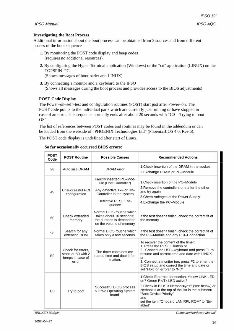
So far occasionally occurred BIOS errors:
POSTCode POST Routine Possible Causes Recommended Actions
28 Auto size DRAM DRAM error1.Check insertion of the DRAM in the socket
2.Exchange DRAM or PC–Module
Faultily inserted PC–Mod-ule (Host Controller) 1.Check insertion of the PC–Module
49 Unsuccessful PCIconfiguration
Any defective Tx– or Rx–Controller in the system
2.Remove the controllers one after the otherand try again
3 Check voltages of the Power Supplyg
Defective RESET se-quence
3.Check voltages of the Power Supply
4.Exchange the PC–Module
60 Check extendedmemory
Normal BIOS routine whichtakes about 10 seconds;
the duration is dependendon the volume of memory
If the test doesn’t finish, check the correct fit ofthe memory.
98 Search for anyextention ROM
Normal BIOS routine whichtakes only a few seconds
If the test doesn’t finish, check the correct fit ofthe PC–Module and any PCI–Connection.
B0
Check for errors,stops at B0 with 2beeps in case of
error
The timer containes cor-rupted time and date infor-
mation.
To recover the content of the timer:1. Press the RESET button or2. Connect an USB–keyboard and press F1 toresume and correct time and date with LINUXor3. Connect a monitor too, press F2 to enter theBIOS setup and correct the time and date orset “Hold on errors” to “NO”
C0 Try to bootSuccessful BIOS processbut “No Operating System
found”
1.Check Ethernet connection. Yellow LINK LEDon? Green Rx/Tx LED active?
2.Check in BIOS if Netboot=yes? (see below) orNetboot is at the top of the list in the submenu“Boot Device Priority”andset the item “Onboard LAN RPL ROM” to “En-abled”

IPSO AQS
IPSO 19”
IPSO Manual
17
BRUKER BioSpin Computer/Hardware Manual
2007–04–27
Note: The PC–Module can be pulled off after removing the 4 screws on topof the Module.
To check or exchange the DRAM, the module has to be opened afterremoving the 2 screws at its bottom side.
Acoustic Beep CodesAdditional to the POST code display some POST routines sound a beep code on error. Thisbeep code is derived from the hexadecimal POST code of the failing test as follows:
1. The 8–bit error code is broken down to four 2–bit groups.
2. Each group is made one–based (1 through 4) by adding 1.
3. Short beeps are generated for the number in each group.
Example: POST code 16h = 00 01 01 10 = 1–2–2–3 beeps
The “Hyper Terminal” or “cu” windowThe boot messages of the IPSO–OS (LINUX) can be printed in a window of the TOPSPIN–PC.This needs a RS232 connection from tty0 of IPSO to a COM port of the TOPSPIN–PC. For de-tails see the TOPSPIN Installation Guide.
Monitor and Keyboard at IPSOThe most detailed information about the boot process can only be obtained by connecting anadditional monitor and a keyboard to the connectors inside of the case. It is then possible towatch the BIOS and Linux Messages during the boot sequence and to enter the BIOS setup util-ity.
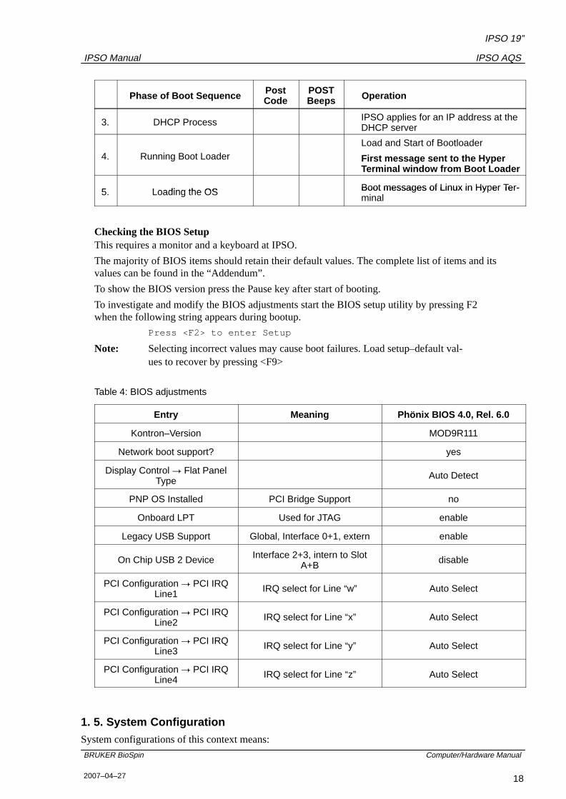
Boot Sequence
Phase of Boot Sequence PostCode
POSTBeeps Operation
1. Power On
16h 1–2–2–3 Check BIOS ROM checksum
20h 1–3–1–1 Test DRAM refresh
22h 1–3–1–3 Test 8742 Keyboard Controller
2Ch 1–3–4–1 RAM failure on address line xxxx*
2Eh 1–3–4–3 RAM failure on data bits xxxx* of lowbyte of memory
30h 1–4–1–1 RAM failure on data bits xxxx* of highbyte of memory
2 Running POST Code 46h 2–1–2–3 Check ROM copyright notice2. Running POST Code4Ah
58h 2–2–3–1 Test for unexpected interrupts
59h
6Eh
87h
98h 1–2 Search for option ROMs
B0h 1–1 Halt on error
C0h Try to boot
IPSO AQS
IPSO 19”
IPSO Manual
18
BRUKER BioSpin Computer/Hardware Manual
2007–04–27
OperationPOSTBeeps
PostCodePhase of Boot Sequence
3. DHCP Process IPSO applies for an IP address at theDHCP server
Load and Start of Bootloader4. Running Boot Loader First message sent to the Hyper
Terminal window from Boot Loader
5 Loading the OS Boot messages of Linux in Hyper Ter-5. Loading the OS Boot messages of Linux in Hy er Ter-minal
Checking the BIOS SetupThis requires a monitor and a keyboard at IPSO.
The majority of BIOS items should retain their default values. The complete list of items and itsvalues can be found in the “Addendum”.
To show the BIOS version press the Pause key after start of booting.
To investigate and modify the BIOS adjustments start the BIOS setup utility by pressing F2when the following string appears during bootup.
Press <F2> to enter Setup
Note: Selecting incorrect values may cause boot failures. Load setup–default val-ues to recover by pressing <F9>
Table 4: BIOS adjustments
Entry Meaning Phönix BIOS 4.0, Rel. 6.0
Kontron–Version MOD9R111
Network boot support? yes
Display Control � Flat PanelType Auto Detect
PNP OS Installed PCI Bridge Support no
Onboard LPT Used for JTAG enable
Legacy USB Support Global, Interface 0+1, extern enable
On Chip USB 2 Device Interface 2+3, intern to SlotA+B disable
PCI Configuration � PCI IRQLine1 IRQ select for Line “w” Auto Select
PCI Configuration � PCI IRQLine2 IRQ select for Line “x” Auto Select
PCI Configuration � PCI IRQLine3 IRQ select for Line “y” Auto Select
PCI Configuration � PCI IRQLine4 IRQ select for Line “z” Auto Select
1. 5. System ConfigurationSystem configurations of this context means:

IPSO AQS
IPSO 19”
IPSO Manual
19
BRUKER BioSpin Computer/Hardware Manual
2007–04–27
1. During boot the BIOS checks for available hardware on the PCI bus, e.g. inserted controller or PCIcards. It recognizes the bus layout, scans all possible slots (sites) for devices, reads the type of thedevices and their required amount of address space, defines and sets the base address of each de-vice, lists all devices found and determines which interrupt line they are connected to.
2. After boot, the AQ–Driver uses the list of the BIOS, reads some additional registers of some de-vices and gains the necessary information to decide on which IPSO host model (IPSO 19” Unit orIPSO AQS) the software is coming up.
There is no active role for the user to influence this process other than changing the arrangement ofinserted controllers and PCI cards. And normally this should not be necessary.
Modifying the arrangement changes the device number of each device and could alter the follow-ing situations:
� Which controllers can communicate with each other without having to goover a bridge. This is normally irrelevant.
� Which of the controllers share the same interrupt line with each other andwith other devices, e.g. the Ethernet or the tty ports.
� To which priority level of the interrupt controller (there are 15) the inter-rupt of a device has been routed
The PCI bus contains 4 interrupt lines (INTw, INTx, INTy, INTz named in BIOS as Line1, Line2,Line3, Line4). The distribution of each controller slot interrupt to one of these lines is hard wired.
Table 5: Interrupt distribution of the IPSO 19” Unit
Controller Slot
1 2 3 4 5 6 7 8 9PCI 1 PCI 2
rctrl tctrl fctrl 1 fctrl 2 fctrl 3 fctrl 4 fctrl 5 fctrl 6 fctrl 7PCI 1 PCI 2
Line 1 x x
Line 2 x x x
Line 3 x x x
Line 4 x x x
Table 6: Interrupt distribution of the IPSO AQS
Controller Slot
rctrl tctrl fctrl 1 fctrl 2 fctrl 3 gctrl PCI 1 PCI 2
Line 1 x x
Line 2 x x
Line 3 x
Line 4 x x x
The decision about routing of Line1/2/3/4 to any of the interrupt priority levels (IRQ) and sharing itwith further interrupt sources is made by the BIOS, provided the BIOS parameter “PCI IRQ Line”is set to “Auto Select”. These routings can be checked in a LINUX shell with:

IPSO AQS
IPSO 19”
IPSO Manual
20
BRUKER BioSpin Computer/Hardware Manual
2007–04–27
cat /proc/interrupts
We do not recommend replacing “Auto Select” by a special IRQ level.
highest Interrupt Priority Order lowest
IRQ 0 1 8 9 10 11 12 13 14 15 3 4 5 6 7
Recognition of the host model
Recognition of the host model and the version of the installed controller will be performed by theAQ–Driver of LINUX in following steps:
1. Search for a PLX device with Subdevice–ID = 0x0200 and the IMBF version register implemented.
2. Read the content of the IMBF version register
3. If IMBF=0xFFFF or 0x0000, � IPSO 19” Unit
1. Read the version register SLOT_BRDV on each Controller
2. SLOT_BRDV=0xXFXX or 0xX0XX � 2MB external RAM on this Con-troller and DSP TMS320C6415SLOT_BRDV=0xX1XX � 16MB external RAM on this Controller andDSP TMS320C6415SLOT_BRDV=0xX2XX � 128MB external RAM on this Controller andDSP TMS320C6455
4. If IMBF= 0x0001, � IPSO AQS � IPSO AQS HOST including RxController with 2MB exter-nal RAM and DSP TMS320C6415
1. Read the board version of IPSO AQS ACQ out of the T_BRDV register
2. T_BRDV=0x0000 � TxController with 16MB external RAM and DSPTMS320C6415 on IPSO AQS ACQ
3. T_BRDV=0x0200 � TxController with 128MB external RAM and DSPTMS320C6455 on IPSO AQS ACQ
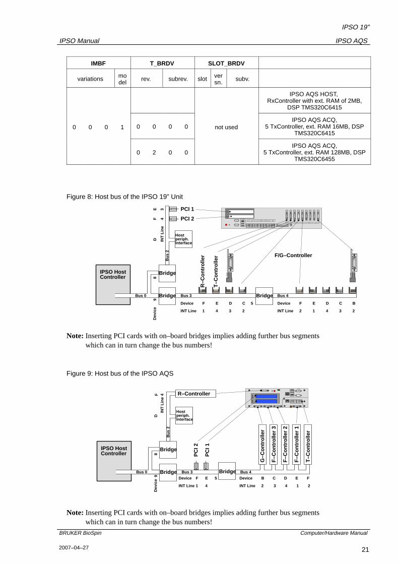
Table 7: IPSO Versions
IMBF T_BRDV SLOT_BRDV
variations model rev. subrev. slot ver
sn. subv.
F F F FIPSO 19” Unit
0 0 0 0IPSO 19” Unit
X F X X TxController of IPSO 19” Unit
not used X 0 X X
TxController of IPSO 19 Unitext RAM 2MB, DSP TMS320C6415
X 1 X X TxController of IPSO 19” Unitext RAM 16MB, DSP TMS320C6415
X 2 X X TxController of IPSO 19” Unitext RAM 128MB, DSP TMS320C6455
IPSO AQS
IPSO 19”
IPSO Manual
21
BRUKER BioSpin Computer/Hardware Manual
2007–04–27
IMBF SLOT_BRDVT_BRDV
variations subv.versn.slotsubrev.rev.mo
del
IPSO AQS HOST, RxController with ext. RAM of 2MB,
DSP TMS320C6415
0 0 0 1 0 0 0 0 not usedIPSO AQS ACQ,
5 TxController, ext. RAM 16MB, DSPTMS320C6415
0 2 0 0IPSO AQS ACQ,
5 TxController, ext. RAM 128MB, DSPTMS320C6455
Figure 8: Host bus of the IPSO 19” Unit
BCDEFDevice
Bridge Bus 4
CDEFDevice
Bus 3Bridge
T–C
ontr
olle
r F/G–Controller
R–C
ontr
olle
r
Bridge
Bus
2
89
Dev
ice
PCI 1
PCI 2
Bus 0
FE
IPSO HostController
Hostperiph.Interface
D
5
2341INT Line 23412INT Line
34
INT
Lin
e
Note: Inserting PCI cards with on–board bridges implies adding further bus segmentswhich can in turn change the bus numbers!
Figure 9: Host bus of the IPSO AQS
FEDCBDevice
Bridge Bus 4
EFDevice
Bus 3Bridge
F–C
ontr
olle
r 2
Bridge
Bus
2
89
Dev
ice
Bus 0
F
IPSO HostController
Hostperiph.Interface
D
PC
I 1
PC
I 2
F–C
ontr
olle
r 3
G–C
ontr
olle
r
F–C
ontr
olle
r 1
T–C
ontr
olle
r
R–Controller
5
21432INT Line41INT Line
4IN
T L
ine
ÉÉ ÉÎÎÎÉÉ
ÉÉ
ÉÉ
Note: Inserting PCI cards with on–board bridges implies adding further bus segmentswhich can in turn change the bus numbers!
IPSO AQS
IPSO 19”
IPSO Manual
22
BRUKER BioSpin Computer/Hardware Manual
2007–04–27
Checking the ConfigurationModification of the system (by inserting or removing controllers or PCI cards) should always befollowed by checking the system–recognized structure against the expected one. For instance, “hasthe system accurately recognized the number and the type of all inserted controllers?”.
Starting the ipsotest when logged in at the IPSO
root@IPSO:/opt/test> ipsotest ↵
returns a list of all recognized controllers, their bus and device numbers and their application spe-cific utilization. Bus bridges, general PCI devices and interrupt routings are not shown.
A complete list of all PCI devices and interrupt routings is shown by typing
root@IPSO:/opt/test> cat /proc/pci ↵
Note: Devices on bus0 and bus1 are not application relevant!
1. 6. Power Supply
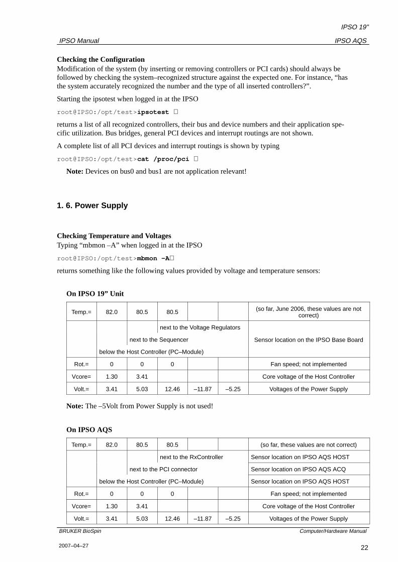
Checking Temperature and VoltagesTyping “mbmon –A” when logged in at the IPSO
root@IPSO:/opt/test> mbmon –A↵
returns something like the following values provided by voltage and temperature sensors:
On IPSO 19” Unit
Temp.= 82.0 80.5 80.5 (so far, June 2006, these values are notcorrect)
next to the Voltage Regulators
next to the Sequencer Sensor location on the IPSO Base Board
below the Host Controller (PC–Module)
Rot.= 0 0 0 Fan speed; not implemented
Vcore= 1.30 3.41 Core voltage of the Host Controller
Volt.= 3.41 5.03 12.46 –11.87 –5.25 Voltages of the Power Supply
Note: The –5Volt from Power Supply is not used!
On IPSO AQS
Temp.= 82.0 80.5 80.5 (so far, these values are not correct)
next to the RxController Sensor location on IPSO AQS HOST
next to the PCI connector Sensor location on IPSO AQS ACQ
below the Host Controller (PC–Module) Sensor location on IPSO AQS HOST
Rot.= 0 0 0 Fan speed; not implemented
Vcore= 1.30 3.41 Core voltage of the Host Controller
Volt.= 3.41 5.03 12.46 –11.87 –5.25 Voltages of the Power Supply
IPSO AQS
IPSO 19”
IPSO Manual
23
BRUKER BioSpin Computer/Hardware Manual
2007–04–27
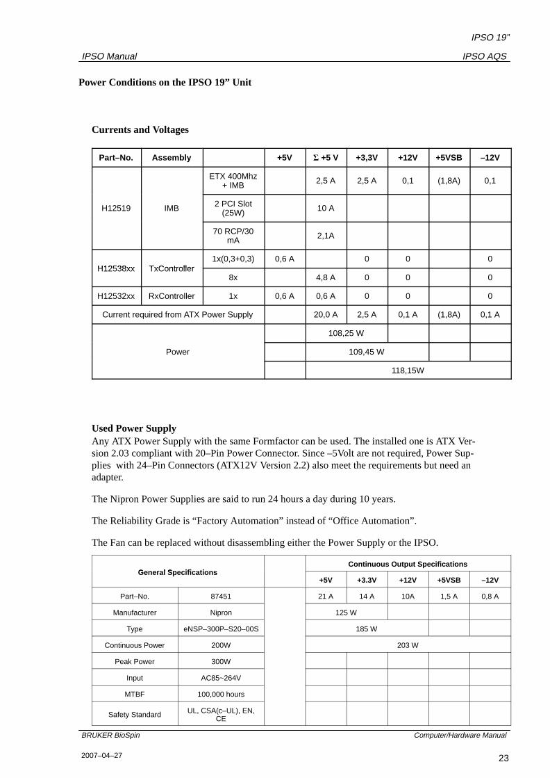
Power Conditions on the IPSO 19” Unit
Currents and Voltages
Part–No. Assembly +5V � +5 V +3,3V +12V +5VSB –12V
ETX 400Mhz+ IMB 2,5 A 2,5 A 0,1 (1,8A) 0,1
H12519 IMB 2 PCI Slot(25W) 10 A
70 RCP/30mA 2,1A
H12538xx TxController1x(0,3+0,3) 0,6 A 0 0 0
H12538xx TxController8x 4,8 A 0 0 0
H12532xx RxController 1x 0,6 A 0,6 A 0 0 0
Current required from ATX Power Supply 20,0 A 2,5 A 0,1 A (1,8A) 0,1 A
108,25 W
Power 109,45 W
118,15W
Used Power SupplyAny ATX Power Supply with the same Formfactor can be used. The installed one is ATX Ver-sion 2.03 compliant with 20–Pin Power Connector. Since –5Volt are not required, Power Sup-plies with 24–Pin Connectors (ATX12V Version 2.2) also meet the requirements but need anadapter.
The Nipron Power Supplies are said to run 24 hours a day during 10 years.
The Reliability Grade is “Factory Automation” instead of “Office Automation”.
The Fan can be replaced without disassembling either the Power Supply or the IPSO.
General SpecificationsContinuous Output Specifications
General Specifications+5V +3.3V +12V +5VSB –12V
Part–No. 87451 21 A 14 A 10A 1,5 A 0,8 A
Manufacturer Nipron 125 W
Type eNSP–300P–S20–00S 185 W
Continuous Power 200W 203 W
Peak Power 300W
Input AC85~264V
MTBF 100,000 hours
Safety Standard UL, CSA(c–UL), EN,CE
IPSO AQS
IPSO 19”
IPSO Manual
24
BRUKER BioSpin Computer/Hardware Manual
2007–04–27
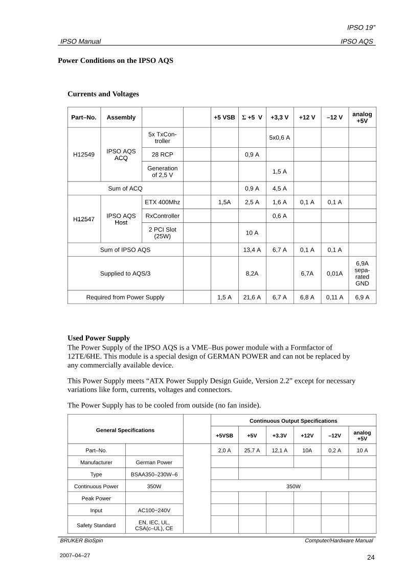
Power Conditions on the IPSO AQS
Currents and Voltages
Part–No. Assembly +5 VSB � +5 V +3,3 V +12 V –12 V analog+5V
5x TxCon-troller 5x0,6 A
H12549 IPSO AQSACQ 28 RCP 0,9 AACQ
Generationof 2,5 V 1,5 A
Sum of ACQ 0,9 A 4,5 A
ETX 400Mhz 1,5A 2,5 A 1,6 A 0,1 A 0,1 A
H12547 IPSO AQSHost
RxController 0,6 AH12547 Host2 PCI Slot
(25W) 10 A
Sum of IPSO AQS 13,4 A 6,7 A 0,1 A 0,1 A
Supplied to AQS/3 8,2A 6,7A 0,01A
6,9Asepa-ratedGND
Required from Power Supply 1,5 A 21,6 A 6,7 A 6,8 A 0,11 A 6,9 A
Used Power SupplyThe Power Supply of the IPSO AQS is a VME–Bus power module with a Formfactor of12TE/6HE. This module is a special design of GERMAN POWER and can not be replaced byany commercially available device.
This Power Supply meets “ATX Power Supply Design Guide, Version 2.2” except for necessaryvariations like form, currents, voltages and connectors.
The Power Supply has to be cooled from outside (no fan inside).
Continuous Output Specifications
General Specifications+5VSB +5V +3.3V +12V –12V analog
+5V
Part–No. 2,0 A 25,7 A 12,1 A 10A 0,2 A 10 A
Manufacturer German Power
Type BSAA350–230W–6
Continuous Power 350W 350W
Peak Power
Input AC100~240V
Safety Standard EN, IEC, UL,CSA(c–UL), CE
IPSO AQS
IPSO 19”
IPSO Manual
25
BRUKER BioSpin Computer/Hardware Manual
2007–04–27
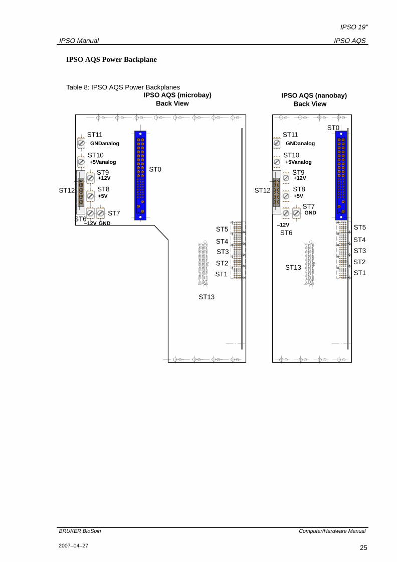
IPSO AQS Power Backplane
Table 8: IPSO AQS Power BackplanesIPSO AQS (nanobay)
GNDanalog
+5Vanalog
+12V
+5V
–12V
GND
ST0
ST1
ST2
ST4
ST3
ST5
ST12
ST7
ST8
ST9
ST10
ST11
ST6
ST13
Back View
GNDanalog
+5Vanalog
+12V
+5V
–12V GND
ST0
ST1
ST2
ST4
ST3
ST5
ST12
ST7
ST8
ST9
ST10
ST11
ST6
ST13
IPSO AQS (microbay)Back View