IP4264CZ8-20; IP4264CZ8-40 Integrated USIM/SIM …...an Universal Subscriber Identity Module (USIM)...
13
Important notice Dear Customer, On 7 February 2017 the former NXP Standard Product business became a new company with the tradename Nexperia. Nexperia is an industry leading supplier of Discrete, Logic and PowerMOS semiconductors with its focus on the automotive, industrial, computing, consumer and wearable application markets In data sheets and application notes which still contain NXP or Philips Semiconductors references, use the references to Nexperia, as shown below. Instead of http://www.nxp.com, http://www.philips.com/ or http://www.semiconductors.philips.com/, use http://www.nexperia.com Instead of [email protected] or [email protected], use [email protected] (email) Replace the copyright notice at the bottom of each page or elsewhere in the document, depending on the version, as shown below: - © NXP N.V. (year). All rights reserved or © Koninklijke Philips Electronics N.V. (year). All rights reserved Should be replaced with: - © Nexperia B.V. (year). All rights reserved. If you have any questions related to the data sheet, please contact our nearest sales office via e-mail or telephone (details via [email protected]). Thank you for your cooperation and understanding, Kind regards, Team Nexperia
Transcript of IP4264CZ8-20; IP4264CZ8-40 Integrated USIM/SIM …...an Universal Subscriber Identity Module (USIM)...

Important notice Dear Customer, On 7 February 2017 the former NXP Standard Product business became a new company with the tradename Nexperia. Nexperia is an industry leading supplier of Discrete, Logic and PowerMOS semiconductors with its focus on the automotive, industrial, computing, consumer and wearable application markets In data sheets and application notes which still contain NXP or Philips Semiconductors references, use the references to Nexperia, as shown below. Instead of http://www.nxp.com, http://www.philips.com/ or http://www.semiconductors.philips.com/, use http://www.nexperia.com Instead of [email protected] or [email protected], use [email protected] (email) Replace the copyright notice at the bottom of each page or elsewhere in the document, depending on the version, as shown below: - © NXP N.V. (year). All rights reserved or © Koninklijke Philips Electronics N.V. (year). All rights reserved Should be replaced with: - © Nexperia B.V. (year). All rights reserved. If you have any questions related to the data sheet, please contact our nearest sales office via e-mail or telephone (details via [email protected]). Thank you for your cooperation and understanding,
Kind regards,
Team Nexperia

1. Product profile
1.1 General descriptionThe IP4264CZ8-20 and IP4264CZ8-40 are 3-channel RC low-pass filter arrays which are designed to provide filtering of undesired RF signals in the 800 MHz-to-6000 MHz frequency band. In addition, the IP4264CZ8-20 and IP4264CZ8-40 incorporate diodes to provide protection to downstream components from ElectroStatic Discharge (ESD) voltages up to ±25 kV contact and higher than ±25 kV air discharge far exceeding IEC 61000-4-2, level 4.
Both IP4264CZ8-20 and IP4264CZ8-40 support ESD protection of the USB data pins of an Universal Subscriber Identity Module (USIM) interface as well as the digital standard SIM interface ESD protection and ElectroMagnetic Interface (EMI) filtering.
The IP4264CZ8-20 and IP4264CZ8-40 are fabricated using monolithic silicon technology. They integrate three resistors and seven high-level ESD protection diodes in a 0.4 mm pitch 8-pin Micropak (compatible with Quad Flat-pack No-leads (QFN)) lead-free plastic package with a height of only 0.5 mm.
These features make the IP4264CZ8-20 and IP4264CZ8-40 ideal for use in applications requiring component miniaturization such as mobile phone handsets, cordless telephones and personal digital devices.
The devices are also available in Wafer Level Chip-Size Package (WLCSP): WLCSP11 (for USIM) with 0.4 mm pitch (IP4365CX11), and WLCSP8 (for SIM) with both 0.4 mm pitch (IP4364CX8/LF) and 0.5 mm pitch (IP4064CX8/LF).
1.2 Features and benefitsPb-free, Restriction of Hazardous Substances (RoHS) compliant and free of halogen and antimony (Dark Green compliant)3-channel SIM card interface with integrated RC-filter array and SIM voltage ESD protection2 USIM (USB1.1) compliant ESD protection diodes with 20 pF channel capacitanceIntegrated 100 Ω/100 Ω/47 Ω series channel resistorsTotal channel capacitance of 20 pF (IP4264CZ8-20) or 40 pF (IP4264CZ8-40)Downstream ESD protection up to ±25 kV (contact) according to IEC 61000-4-2Micropak (QFN compatible) plastic package with 0.4 mm pitchAlso available in WLCSP11: IP4365CX11 (USIM interface) and in WLCSP8: IP4364CX8/LF (0.4 mm pitch) and IP4064CX8/LF or IP4044CX8/LF (both using 0.5 mm pitch, SIM interface)
IP4264CZ8-20; IP4264CZ8-40Integrated USIM/SIM card passive filter arrays with ESD protectionRev. 3 — 22 July 2010 Product data sheet

NXP Semiconductors IP4264CZ8-20; IP4264CZ8-40Integrated USIM/SIM card passive filter arrays with ESD protection
1.3 ApplicationsUSIM and SIM interfaces in e.g. cellular and Personal Communication System (PCS) mobile handsets
2. Pinning information
3. Ordering information
4. Marking
Table 1. PinningPin Description Simplified outline Graphic symbol1 and 8 filter channel 1
2 and 7 filter channel 2
3 and 6 filter channel 3
4 and 5 ESD protection
GND ground Transparenttop view
1 4
8 5
018aaa015
100 Ω
R1
47 Ω
R2
100 Ω
R3
1
2
3
4
8
7
6
5
Table 2. Ordering informationType number Package
Name Description VersionIP4264CZ8-20 HXSON8U plastic thermal enhanced extremely thin small outline package; no leads;
8 terminals; UTLP based; body 1.35 × 1.7 × 0.5 mmSOT983-1
IP4264CZ8-40
Table 3. Marking codesType number Marking codeIP4264CZ8-20 N2
IP4264CZ8-40 N4
IP4264CZ8-20_IP4264CZ8-40 All information provided in this document is subject to legal disclaimers. © NXP B.V. 2010. All rights reserved.
Product data sheet Rev. 3 — 22 July 2010 2 of 12
NXP Semiconductors IP4264CZ8-20; IP4264CZ8-40Integrated USIM/SIM card passive filter arrays with ESD protection
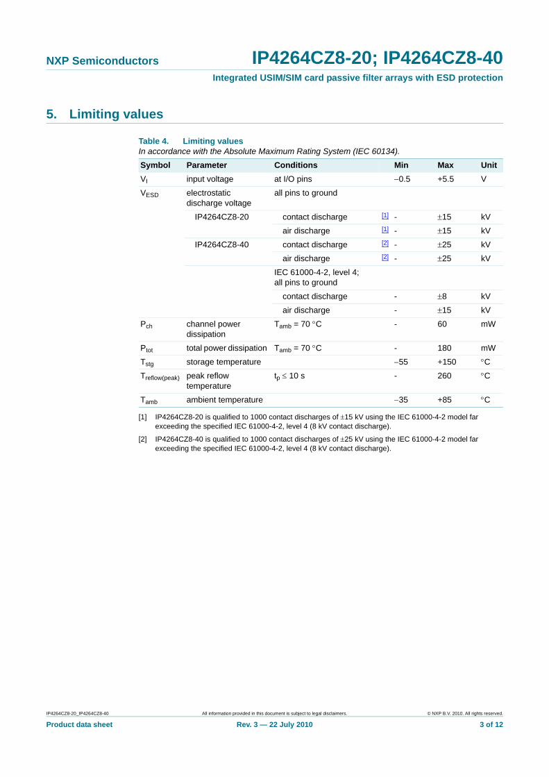
5. Limiting values
[1] IP4264CZ8-20 is qualified to 1000 contact discharges of ±15 kV using the IEC 61000-4-2 model far exceeding the specified IEC 61000-4-2, level 4 (8 kV contact discharge).
[2] IP4264CZ8-40 is qualified to 1000 contact discharges of ±25 kV using the IEC 61000-4-2 model far exceeding the specified IEC 61000-4-2, level 4 (8 kV contact discharge).
Table 4. Limiting valuesIn accordance with the Absolute Maximum Rating System (IEC 60134).
Symbol Parameter Conditions Min Max UnitVI input voltage at I/O pins −0.5 +5.5 V
VESD electrostatic discharge voltage
all pins to ground
IP4264CZ8-20 contact discharge [1] - ±15 kV
air discharge [1] - ±15 kV
IP4264CZ8-40 contact discharge [2] - ±25 kV
air discharge [2] - ±25 kV
IEC 61000-4-2, level 4; all pins to ground
contact discharge - ±8 kV
air discharge - ±15 kV
Pch channel power dissipation
Tamb = 70 °C - 60 mW
Ptot total power dissipation Tamb = 70 °C - 180 mW
Tstg storage temperature −55 +150 °C
Treflow(peak) peak reflow temperature
tp ≤ 10 s - 260 °C
Tamb ambient temperature −35 +85 °C
IP4264CZ8-20_IP4264CZ8-40 All information provided in this document is subject to legal disclaimers. © NXP B.V. 2010. All rights reserved.
Product data sheet Rev. 3 — 22 July 2010 3 of 12

NXP Semiconductors IP4264CZ8-20; IP4264CZ8-40Integrated USIM/SIM card passive filter arrays with ESD protection
6. Characteristics
[1] Guaranteed by design.
[2] Total line capacitance including diode capacitance, per channel.
[3] Measured between pins 4 and 5.
Table 5. Channel resistanceTamb = 25 °C unless otherwise specified.
Symbol Parameter Conditions Min Typ Max UnitRs(ch) channel series
resistanceR1, R3 75 100 125 Ω
R2 35.2 47 58.8 Ω
Table 6. Channel characteristicsTamb = 25 °C unless otherwise specified.
Symbol Parameter Conditions Min Typ Max UnitIP4264CZ8-20Cch channel capacitance f = 1 MHz [1][2]
Vbias(DC) = 0 V - 17 20 pF
Vbias(DC) = 2.5 V - 11 15 pF
IP4264CZ8-40Cch channel capacitance f = 1 MHz [1][2]
Vbias(DC) = 0 V - 35 40 pF
Vbias(DC) = 2.5 V - 23 28 pF
IP4264CZ8-20; IP4264CZ8-40Cd diode capacitance f = 1 MHz [3]
Vbias(DC) = 0 V 12 16 20 pF
Vbias(DC) = 2.5 V 8 11 14 pF
IRM reverse leakage current
VI = 3 V - - 50 nA
VBR breakdown voltage Itest = 1 mA 6 - 10 V
IP4264CZ8-20_IP4264CZ8-40 All information provided in this document is subject to legal disclaimers. © NXP B.V. 2010. All rights reserved.
Product data sheet Rev. 3 — 22 July 2010 4 of 12

NXP Semiconductors IP4264CZ8-20; IP4264CZ8-40Integrated USIM/SIM card passive filter arrays with ESD protection
7. Application information
7.1 Insertion lossThe IP4264CZ8-20 and IP4264CZ8-40 are mainly designed as EMI/Radio Frequency Interference (RFI) filters for SIM card interfaces. The setup for measuring the return loss is shown in Figure 1.
The insertion loss in a 50 Ω system for all three channels of the IP4264CZ8-20 with a line capacitance of ≤ 20 pF total channel capacitance is shown in Figure 2.
And the insertion loss for IP4264CZ8-40 with a line capacitance of ≤ 40 pF channel capacitance is shown in Figure 3.
Fig 1. Frequency response setup
Cch = 20 pF(1) Pin 2 to 7(2) Pin 1 to 8(3) Pin 3 to 6
Cch = 40 pF(1) Pin 2 to 7(2) Pin 1 to 8(3) Pin 3 to 6
Fig 2. Frequency response curves for IP4264CZ8-20 Fig 3. Frequency response curves for IP4264CZ8-40
018aaa016
50 Ω
Vgen
50 Ω
DUTOUTIN
TEST BOARD
018aaa017
−20
−30
−10
0
S21(dB)
−40
f (MHz)10−1 1041031 10210
(1)
(2)
(3)
018aaa018
−20
−30
−10
0
S21(dB)
−40
f (MHz)10−1 1041031 10210
(1)
(2)
(3)
IP4264CZ8-20_IP4264CZ8-40 All information provided in this document is subject to legal disclaimers. © NXP B.V. 2010. All rights reserved.
Product data sheet Rev. 3 — 22 July 2010 5 of 12

NXP Semiconductors IP4264CZ8-20; IP4264CZ8-40Integrated USIM/SIM card passive filter arrays with ESD protection
7.2 CrosstalkThe setup for measuring crosstalk between channels in a 50 Ω system is shown in Figure 4. The crosstalk for the IP4264CZ8-20 is shown in Figure 5 and Figure 6 for the IP4264CZ8-40. Unused channels are terminated with a 50 Ω resistor to ground.
Fig 4. Crosstalk measurement setup
Cch = 20 pF(1) Pin 1 to 7(2) Pin 2 to 6(3) Pin 3 to 8
Cch = 40 pF(1) Pin 1 to 7(2) Pin 2 to 6(3) Pin 3 to 8
Fig 5. Crosstalk behavior for IP4264CZ8-20 Fig 6. Crosstalk behavior for IP4264CZ8-40
018aaa019
50 Ω
Vgen
50 Ω
DUTOUT2IN1
TEST BOARD
50 Ω
OUT1
50 Ω
IN2
018aaa020
−60
−40
−80
−20
0
S21(dB)
−100
f (MHz)10−1 1041031 10210
(1)
(2)(3)
018aaa021
−60
−40
−80
−20
0
S21(dB)
−100
f (MHz)10−1 1041031 10210
(1)
(2)(3)
IP4264CZ8-20_IP4264CZ8-40 All information provided in this document is subject to legal disclaimers. © NXP B.V. 2010. All rights reserved.
Product data sheet Rev. 3 — 22 July 2010 6 of 12

NXP Semiconductors IP4264CZ8-20; IP4264CZ8-40Integrated USIM/SIM card passive filter arrays with ESD protection
7.3 USIM interface application schematicThe application schematic diagram depicted in Figure 7 demonstrates how the NXP SIM card EMI filter and ESD protection devices IP4264CZ8 are used in a typical USIM interface application.
For example, in case a standard SIM interface without USB1.1 is used, the two single diodes (pins 4 and 5) can protect the VSIM line.
Please note that this is only one example dependent on layout constraints e.g. channels 1 to 8 can be swapped with channels 3 to 6.
Also, the USB interface ESD protection pins 4 and 5 can be exchanged. Due to both sides of the devices containing identical protection diodes, baseband and SIM card side can be swapped, too (pin 1 with pin 8, pin 2 with pin 7 etc.).
Fig 7. USIM application schematic for IP4264CZ8
6
7
8
5
1
2
3
BASEBAND
VSIM
RST
CLK
CENTER GROUND PAD
SIM CARD4
D+
D−USB
VSIMprotection
diode
VCC GND
RST SPU
AUX 1 AUX 2
CLK I/O
I/O
R3
100ΩR2
R1
100Ω
47Ω
018aaa022
IP4264CZ8-20_IP4264CZ8-40 All information provided in this document is subject to legal disclaimers. © NXP B.V. 2010. All rights reserved.
Product data sheet Rev. 3 — 22 July 2010 7 of 12

NXP Semiconductors IP4264CZ8-20; IP4264CZ8-40Integrated USIM/SIM card passive filter arrays with ESD protection
8. Package outline
Fig 8. Package outline SOT983-1 (HXSON8U)
REFERENCESOUTLINEVERSION
EUROPEANPROJECTION
ISSUE DATEIEC JEDEC JEITA
SOT983-1 - - -- - -
SOT983-1
07-01-1207-11-14
UNIT Amax
mm 0.5 0.050.00
0.250.15
1.751.65
1.51.3
1.41.3
0.50.3 1.2 0.35
0.15 0.05
A1
DIMENSIONS (mm are the original dimensions)
HXSON8U: plastic thermal enhanced extremely thin small outline package; no leads;8 terminals; UTLP based; body 1.35 x 1.7 x 0.5 mm
0 0.5 1 mm
scale
b D Dh E Eh e
0.4
e1 L v
0.1
w y
0.05
L1
0.090.00
y1
0.1
X
B A
terminal 1index area
D
E
Cy1
C
y
detail X
A
A1
b
e1
e
1/2 e
AC Bv M
Cw M
terminal 1index area
Dh
Eh
L1L
41
8 5
IP4264CZ8-20_IP4264CZ8-40 All information provided in this document is subject to legal disclaimers. © NXP B.V. 2010. All rights reserved.
Product data sheet Rev. 3 — 22 July 2010 8 of 12

NXP Semiconductors IP4264CZ8-20; IP4264CZ8-40Integrated USIM/SIM card passive filter arrays with ESD protection
9. Revision history
Table 7. Revision historyDocument ID Release date Data sheet status Change notice SupersedesIP4264CZ8-20_IP4264CZ8-40 v.3
20100722 Product data sheet - IP4264CZ8-20_IP4264CZ8-40_2
Modifications: • Section 1 “Product profile”: added USIM application• Table 1 “Pinning”: corrected graphic symbol• Table 6 “Channel characteristics”: added Cd maximum and minimum values• Figure 1, 2, 3, 4, 5 and 6: updated• Section 7.3 “USIM interface application schematic”. added• Section 10 “Legal information”: updated
IP4264CZ8-20_IP4264CZ8-40_2
20090427 Product data sheet - IP4264CZ8-20_IP4264CZ8-40_1
IP4264CZ8-20_IP4264CZ8-40_1
20081106 Objective data sheet - -
IP4264CZ8-20_IP4264CZ8-40 All information provided in this document is subject to legal disclaimers. © NXP B.V. 2010. All rights reserved.
Product data sheet Rev. 3 — 22 July 2010 9 of 12

NXP Semiconductors IP4264CZ8-20; IP4264CZ8-40Integrated USIM/SIM card passive filter arrays with ESD protection
10. Legal information
10.1 Data sheet status
[1] Please consult the most recently issued document before initiating or completing a design.
[2] The term ‘short data sheet’ is explained in section “Definitions”.
[3] The product status of device(s) described in this document may have changed since this document was published and may differ in case of multiple devices. The latest product status information is available on the Internet at URL http://www.nxp.com.
10.2 DefinitionsDraft — The document is a draft version only. The content is still under internal review and subject to formal approval, which may result in modifications or additions. NXP Semiconductors does not give any representations or warranties as to the accuracy or completeness of information included herein and shall have no liability for the consequences of use of such information.
Short data sheet — A short data sheet is an extract from a full data sheet with the same product type number(s) and title. A short data sheet is intended for quick reference only and should not be relied upon to contain detailed and full information. For detailed and full information see the relevant full data sheet, which is available on request via the local NXP Semiconductors sales office. In case of any inconsistency or conflict with the short data sheet, the full data sheet shall prevail.
Product specification — The information and data provided in a Product data sheet shall define the specification of the product as agreed between NXP Semiconductors and its customer, unless NXP Semiconductors and customer have explicitly agreed otherwise in writing. In no event however, shall an agreement be valid in which the NXP Semiconductors product is deemed to offer functions and qualities beyond those described in the Product data sheet.
10.3 DisclaimersLimited warranty and liability — Information in this document is believed to be accurate and reliable. However, NXP Semiconductors does not give any representations or warranties, expressed or implied, as to the accuracy or completeness of such information and shall have no liability for the consequences of use of such information.
In no event shall NXP Semiconductors be liable for any indirect, incidental, punitive, special or consequential damages (including - without limitation - lost profits, lost savings, business interruption, costs related to the removal or replacement of any products or rework charges) whether or not such damages are based on tort (including negligence), warranty, breach of contract or any other legal theory.
Notwithstanding any damages that customer might incur for any reason whatsoever, NXP Semiconductors’ aggregate and cumulative liability towards customer for the products described herein shall be limited in accordance with the Terms and conditions of commercial sale of NXP Semiconductors.
Right to make changes — NXP Semiconductors reserves the right to make changes to information published in this document, including without limitation specifications and product descriptions, at any time and without notice. This document supersedes and replaces all information supplied prior to the publication hereof.
Suitability for use — NXP Semiconductors products are not designed, authorized or warranted to be suitable for use in life support, life-critical or safety-critical systems or equipment, nor in applications where failure or
malfunction of an NXP Semiconductors product can reasonably be expected to result in personal injury, death or severe property or environmental damage. NXP Semiconductors accepts no liability for inclusion and/or use of NXP Semiconductors products in such equipment or applications and therefore such inclusion and/or use is at the customer’s own risk.
Applications — Applications that are described herein for any of these products are for illustrative purposes only. NXP Semiconductors makes no representation or warranty that such applications will be suitable for the specified use without further testing or modification.
Customers are responsible for the design and operation of their applications and products using NXP Semiconductors products, and NXP Semiconductors accepts no liability for any assistance with applications or customer product design. It is customer’s sole responsibility to determine whether the NXP Semiconductors product is suitable and fit for the customer’s applications and products planned, as well as for the planned application and use of customer’s third party customer(s). Customers should provide appropriate design and operating safeguards to minimize the risks associated with their applications and products.
NXP Semiconductors does not accept any liability related to any default, damage, costs or problem which is based on any weakness or default in the customer’s applications or products, or the application or use by customer’s third party customer(s). Customer is responsible for doing all necessary testing for the customer’s applications and products using NXP Semiconductors products in order to avoid a default of the applications and the products or of the application or use by customer’s third party customer(s). NXP does not accept any liability in this respect.
Limiting values — Stress above one or more limiting values (as defined in the Absolute Maximum Ratings System of IEC 60134) will cause permanent damage to the device. Limiting values are stress ratings only and (proper) operation of the device at these or any other conditions above those given in the Recommended operating conditions section (if present) or the Characteristics sections of this document is not warranted. Constant or repeated exposure to limiting values will permanently and irreversibly affect the quality and reliability of the device.
Terms and conditions of commercial sale — NXP Semiconductors products are sold subject to the general terms and conditions of commercial sale, as published at http://www.nxp.com/profile/terms, unless otherwise agreed in a valid written individual agreement. In case an individual agreement is concluded only the terms and conditions of the respective agreement shall apply. NXP Semiconductors hereby expressly objects to applying the customer’s general terms and conditions with regard to the purchase of NXP Semiconductors products by customer.
No offer to sell or license — Nothing in this document may be interpreted or construed as an offer to sell products that is open for acceptance or the grant, conveyance or implication of any license under any copyrights, patents or other industrial or intellectual property rights.
Export control — This document as well as the item(s) described herein may be subject to export control regulations. Export might require a prior authorization from national authorities.
Document status[1][2] Product status[3] Definition
Objective [short] data sheet Development This document contains data from the objective specification for product development.
Preliminary [short] data sheet Qualification This document contains data from the preliminary specification.
Product [short] data sheet Production This document contains the product specification.
IP4264CZ8-20_IP4264CZ8-40 All information provided in this document is subject to legal disclaimers. © NXP B.V. 2010. All rights reserved.
Product data sheet Rev. 3 — 22 July 2010 10 of 12

NXP Semiconductors IP4264CZ8-20; IP4264CZ8-40Integrated USIM/SIM card passive filter arrays with ESD protection
Non-automotive qualified products — Unless this data sheet expressly states that this specific NXP Semiconductors product is automotive qualified, the product is not suitable for automotive use. It is neither qualified nor tested in accordance with automotive testing or application requirements. NXP Semiconductors accepts no liability for inclusion and/or use of non-automotive qualified products in automotive equipment or applications.
In the event that customer uses the product for design-in and use in automotive applications to automotive specifications and standards, customer (a) shall use the product without NXP Semiconductors’ warranty of the product for such automotive applications, use and specifications, and (b) whenever customer uses the product for automotive applications beyond
NXP Semiconductors’ specifications such use shall be solely at customer’s own risk, and (c) customer fully indemnifies NXP Semiconductors for any liability, damages or failed product claims resulting from customer design and use of the product for automotive applications beyond NXP Semiconductors’ standard warranty and NXP Semiconductors’ product specifications.
10.4 TrademarksNotice: All referenced brands, product names, service names and trademarks are the property of their respective owners.
11. Contact information
For more information, please visit: http://www.nxp.com
For sales office addresses, please send an email to: [email protected]
IP4264CZ8-20_IP4264CZ8-40 All information provided in this document is subject to legal disclaimers. © NXP B.V. 2010. All rights reserved.
Product data sheet Rev. 3 — 22 July 2010 11 of 12

NXP Semiconductors IP4264CZ8-20; IP4264CZ8-40Integrated USIM/SIM card passive filter arrays with ESD protection
12. Contents
1 Product profile . . . . . . . . . . . . . . . . . . . . . . . . . . 11.1 General description . . . . . . . . . . . . . . . . . . . . . 11.2 Features and benefits . . . . . . . . . . . . . . . . . . . . 11.3 Applications . . . . . . . . . . . . . . . . . . . . . . . . . . . 22 Pinning information. . . . . . . . . . . . . . . . . . . . . . 23 Ordering information. . . . . . . . . . . . . . . . . . . . . 24 Marking . . . . . . . . . . . . . . . . . . . . . . . . . . . . . . . . 25 Limiting values. . . . . . . . . . . . . . . . . . . . . . . . . . 36 Characteristics. . . . . . . . . . . . . . . . . . . . . . . . . . 47 Application information. . . . . . . . . . . . . . . . . . . 57.1 Insertion loss . . . . . . . . . . . . . . . . . . . . . . . . . . 57.2 Crosstalk. . . . . . . . . . . . . . . . . . . . . . . . . . . . . . 67.3 USIM interface application schematic. . . . . . . . 78 Package outline . . . . . . . . . . . . . . . . . . . . . . . . . 89 Revision history. . . . . . . . . . . . . . . . . . . . . . . . . 910 Legal information. . . . . . . . . . . . . . . . . . . . . . . 1010.1 Data sheet status . . . . . . . . . . . . . . . . . . . . . . 1010.2 Definitions. . . . . . . . . . . . . . . . . . . . . . . . . . . . 1010.3 Disclaimers . . . . . . . . . . . . . . . . . . . . . . . . . . . 1010.4 Trademarks. . . . . . . . . . . . . . . . . . . . . . . . . . . 1111 Contact information. . . . . . . . . . . . . . . . . . . . . 1112 Contents . . . . . . . . . . . . . . . . . . . . . . . . . . . . . . 12
© NXP B.V. 2010. All rights reserved.For more information, please visit: http://www.nxp.comFor sales office addresses, please send an email to: [email protected]
Date of release: 22 July 2010Document identifier: IP4264CZ8-20_IP4264CZ8-40
Please be aware that important notices concerning this document and the product(s)described herein, have been included in section ‘Legal information’.