Ion beam etching of InP based materials - DiVA portal8927/FULLTEXT01.pdf · An ion beam system in...
57
ISRN KTH/HMA/FR-01/2-SE TRITA-HMA REPORT 2001:2 ISSN 1404-0379 Ion beam etching of InP based materials Doctoral thesis by Carl-Fredrik Carlström Laboratory of Semiconductor Materials Department of Microelectronics and Information Technology Royal Institute of Technology Electrum 229, S-164 40 Kista, Sweden Stockholm 2001
Transcript of Ion beam etching of InP based materials - DiVA portal8927/FULLTEXT01.pdf · An ion beam system in...

ISRN KTH/HMA/FR-01/2-SE TRITA-HMA REPORT 2001:2 ISSN 1404-0379
Ion beam etching of InP based materials
Doctoral thesis by
Carl-Fredrik Carlström
Laboratory of Semiconductor Materials
Department of Microelectronics and Information Technology
Royal Institute of Technology Electrum 229, S-164 40 Kista, Sweden
Stockholm 2001


i
Carl-Fredrik Carlström Ion beam etching of InP based materials Department of Microelectronics and Information Technology Royal Institute of Technology S-164 40 Kista, Sweden ISRN KTH/HMA/FR-01/2-SE TRITA-HMA REPORT 2001:2 ISSN 1404-0379
Abstract Dry etching is an important technique for pattern transfer in fabrication of
most opto-electronic devices, since it can provide good control of both structure size and shape even on a sub-micron scale. Unfortunately, this process step may cause damage to the material which is detrimental to device performance. It is therefore an objective of this thesis to develop and investigate low damage etching processes for InP based devices.
An ion beam system in combination with hydrocarbon (CH4) based chemistries is used for etching. At various ion energies and gas flows the etching is performed in two modes, reactive ion beam etching (RIBE) and chemical assisted ion beam etching (CAIBE). How these conditions affect both etch characteristics (e.g. etch rates and profiles, surface morphology and polymer formation) and etch induced damage (on optical and electrical properties) is evaluated and discussed. Attention is also paid to the effects of typical post etching treatments such as annealing on the optical and electrical properties. An important finding is the correlation between as-etched surface morphology and recovery/degradation in photoluminescence upon annealing in PH3. Since this type of atmosphere is typical for crystal regrowth (an important process step in III/V processing) a positive result is imperative. A low ion energy N2/CH4/H2 CAIBE process is developed which not only satisfies this criteria but also exhibits good etch characteristics. This process is used successfully in the fabrication of laser gratings. In addition to this, the ability of the ion beam system to modify the surface morphology in a controllable manner is exploited. By exposing such modified surfaces to AsH3/PH3, a new way to vary size and density of InAs(P) islands formed on the InP surfaces by the As/P exchange reaction is presented.
This thesis also proposes a new etch chemistry, namely trimethylamine ((CH3)3N or TMA), which is a more efficient methyl source compared to CH4 because of the low energy required to break the H3C-N bond. Since methyl radicals are needed for the etching it is presumably a better etching chemistry. A similar investigation as for the CH4 chemistry is performed, and it is found that both in terms of etch characteristics and etch induced damage this new chemistry is superior. Extremely smooth morphologies, low etch induced damage and an almost complete recovery upon annealing can be obtained with this process. Significantly, this is also so at relatively high ion energies which allows higher etch rates. Descriptors: InP, dry etching, ion beam etching, RIBE, CAIBE, hydrocarbon chemistry, trimethylamine, As/P exchange reaction, morpholoy, low damage, AFM, SCM, annealing


iii
Appended papers Paper A Low energy ion beam etching of InP using methane chemistry C. F. Carlström, G. Landgren, and S. Anand, Journal of Vacuum Science and Technology B16(3), (1998) 1018 Paper B Extremely smooth surface morphologies in N2/H2/CH4 based low energy chemically assisted ion beam etching of InP/GaInAsP C. F. Carlström, S. Anand, and G. Landgren, Thin Solid Films 343-344, (1999) 374 Paper C Impact of surface morphology on InAs(P) island formation on InP C. F. Carlström, S. Anand, E. Niemi, and G. Landgren, Institute of Physics Conference Series No. 164, (1999) 141 Paper D Trimethylamine: Novel source for low damage reactive ion beam etching of InP C. F. Carlström, S. Anand, and G. Landgren, Journal of Vacuum Science and Technology B17(6), (1999) 2660 Paper E Polymer free reactive ion beam etching of InP using N2/(CH3)3N C. F. Carlström, S. Anand, and G. Landgren, 2000 Proceeding of InP and Related Materials, Williamsburg, Virginia, 298-301 Paper F Doping landscapes in the nano-meter range by scanning capacitance microscopy S. Anand, C. F. Carlström, E. Rodriguez Messmer, S. Lourdudoss and G. Landgren, Applied Surface Science 144-145, (1999) 525 Paper G Buried heterostructure complex-coupled distributed feedback 1.55 µm lasers fabricated using dry etching processes and quaternary layer overgrowth D. Söderstrom, S. Lourdudoss, C.F. Carlström, S. Anand, M. Kahn, and M. Kamp, Journal of Vacuum Science and Technology B17(6), (1999) 2622 Paper H Characterisation of damage in InP dry-etched using nitrogen containing chemistries C. F. Carlström, and S. Anand, Submitted to Journal of Vacuum Science and Technology B Paper I Scanning Capacitance Microscopy as an in-line evaluation tool for dry etching of semiconductors: A case study with InP S. Anand, O. Douhéret, and C. F. Carlström, Institute of Physics Conference Series (In press)

iv

v
Acronyms III Group three in the periodic system V Group five in the periodic system AC Alternating Current
AES Auger Electron Spectroscopy AFM Atomic Force Microscopy
BH Buried Heterostructure CAIBE Chemically Assisted Ion Beam Etching CC Complex Coupled C-V Capacitance Voltage DC Direct Current DFB Distributed Feedback ECR Electron Cyclotron Resonance FWHM Full Width Half Maximum IBE Ion Beam Etching
HVPE Hydride Vapour Phase Epitaxy ICP Inductively Coupled Plasma I-V Current Voltage LP Liquid Phase MIS Metal Insulator Semiconductor MOVPE Metal Organic Vapour Phase Epitaxy MQW Multiple Quantum Well
MS Metal Semiconductor PL Photoluminescence PLI Photoluminescence Intensity PLY Photoluminescence Yield
QW Quantum Well RBS Rutherford Back Scattering RF Radio Frequency (13.56 MHz) RIE Reactive Ion Etching RIBE Reactive Ion Beam Etching
RMS Root Mean Square SCH Separate Confinement Heterostructure SCM Scanning Capacitance Microscopy
SEM Scanning Electron Microscopy SI Semi Insulating SIMS Secondary Ion Mass Spectroscopy
SMSR Single Mode Suppression Ratio TEM Transmission Electron Microscopy TMA Trimethylamine
UHF Ultra High Frequency XPS X-ray Photoelectron Spectroscopy


vii
Table of Contents ABSTRACT................................................................................................................................................ I APPENDED PAPERS............................................................................................................................ III ACRONYMS.............................................................................................................................................V
1 INTRODUCTION .............................................................................................................................1
2 DRY ETCHING.................................................................................................................................5
2.1 PLASMA PROPERTIES AND DRY ETCHING MECHANISMS...............................................................5 2.2 DRY ETCHING SYSTEMS, REACTORS AND PLASMA SOURCES .......................................................7 2.3 CHEMISTRY FOR ETCHING OF InP/InGaAsP...............................................................................12
2.3.1 Halogen chemistry.................................................................................................................................13 2.3.2 Hydrocarbon chemistry .........................................................................................................................13
3 ETCH PROPERTIES AND CHARACTERISATION TECHNIQUES...................................17
3.1 ETCH PROPERTIES: GEOMETRICAL ASPECTS ..............................................................................17 3.2 ETCH INDUCED DAMAGE: IMPACT ON OPTICAL PROPERTIES......................................................19 3.3 ETCH-INDUCED DAMAGE: IMPACT ON ELECTRICAL PROPERTIES ...............................................21
3.3.1 I-V characteristics of metal-semiconductor contacts............................................................................21 3.3.2 Scanning Capacitance Microscopy (SCM)...........................................................................................22
3.4 ETCH-INDUCED DAMAGE : MATERIAL PROPERTIES....................................................................23
4 GUIDE TO THE PUBLICATIONS..............................................................................................25
5 CONCLUSIONS..............................................................................................................................29
6 SUMMARY OF THE PAPERS.....................................................................................................31
7 LIST OF PUBLICATIONS NOT INCLUDED IN THIS THESIS ...........................................35
8 ACKNOWLEDGEMENT ..............................................................................................................37
9 REFERENCES ................................................................................................................................39


1
1 Introduction It is difficult to imagine how our daily life would be without all the today’s
electronic integrated circuits (IC), opto-electron devices and opto-electronic integrated circuits (OEIC). ICs are found not only in computers, but also in almost all other electronic equipment such as televisions, washing machines, phones etc. Opto-electron devices include semiconductor lasers, light emitting diodes or photo detectors, and are denoted OEIC if they are integrated monolithically with electronic devices. Examples of applications are signal handling in fibre communication systems, CD-ROMs, laser printers, IR-detectors, gas-sensors, night vision goggles etc.
In fabrication of many of these integrated circuits, techniques to isolate certain regions of the semiconductor sample in a controllable manner are essential. One way to do this is to remove the surrounding parts, and possibly also replace them with another material. The removal step can be accomplished by protecting desired regions of the sample and then expose the sample to an aggressive environment, which attacks and removes the unprotected regions. This last step is called etching and is a key technology in the pattern transfer process. Usually a predefined mask pattern is formed on top of the substrate surface, and subsequently the unpatterned regions are removed by etching.
Two main etching techniques can be distinguished: wet etching and dry etching. In wet etching liquid chemicals are used, usually acids, and thereby the name “wet etching”. On the other hand, dry etching employs a gas plasma, and it is due to the lack of liquid chemicals it has earned its name. Here, both ions from the plasma and neutral gas species can react with the substrate. The etching can be (1) physical - energetic ions bombarding the sample and (2) chemical - both ions and gas species reacting spontaneously with the substrate material, forming volatile etch products. Both etching techniques have their pros and cons. Wet etching generates little damage to the material and both equipment and maintenance costs are much lower. On the other hand, dry etching provides good process control and compatibility with an all-vacuum process, and the consumption of materials is also low. Further, the etching can be anisotropic i.e. directional etching.
For many devices anisotropic etching is essential, especially for narrow structures which require a high etch depth. Unfortunately, wet etching is isotropic, (etching occurs in all directions) and crystallographic (etch rates depend on crystal direction), and therefore, adequate dimensional control is difficult to obtain. Exceptions are electrochemical and photo-enhanced wet etching which in special cases can be anisotropic,1 but they do not provide the overall applicability of dry etching. Another advantage of dry-etching is the low process temperature. This is because the plasma provides ions and free radicals, which would otherwise only occur at very high temperatures. In addition, ion bombardment can enhance desorption of otherwise non-volatile species. An excellent example is etching of GaN for which there is yet no existing conventional wet etching process. Due to the strong bond the material is chemically inert to standard acids and bases.1 Using reversed liquid phase epitaxy (LPE) with a Ga melt the semiconductor can be etched with reasonable etch rates, but at very high temperatures (>800 oC).2, 3 Photo-enhanced wet etching is possible but is restricted to n-type GaN.1, 4 Here, dry etching has emerged as the saviour, several processes being developed and established with great success.5-8
The typical regime of interest of the plasma is the low pressure discharge. The pressure ranges from 10-4 - 10 Torr, electron densities from 109 to 1012 cm-3, and electron energies from 1 to 10 eV. A major drawback of dry etching, however, is the

2
etch induced damage, which can degrade device performance. Although, since the start of dry etching, significant improvements in reactor design and development of new etch chemistries have been carried out to achieve low damage processes.
The first dry etching process was ashing of photo-resist masks, and it was introduced as early as 1968.9 For the semiconductor industry it was in 1972- 1973 that plasma etching was recognised. The emerging of NMOS technology required etching of silicon nitride and poly silicon, and dry-etching provided the process reliability and control needed for large scale production. Since then dry etching has been employed for etching many different semiconductor materials, metals and insulators.
The main topic of this thesis is on dry etching of InP and related materials. InP is a III-V semiconductor i.e. it consists of indium and phosphorus, which are elements from group III and V in the periodic table, respectively. The advantageous optical and electrical properties of InP, high electron mobility and direct band gap, make it a good candidate for high frequency electronic applications, fiberoptic communication applications, and their integration. Using InP substrates, compounds such as GaInAs, GaInAsP etc can be grown. These materials are used for making light sources and detectors operating in the infrared region, and covers a wave length (λ) range of 920 - 1670 nm.10 Especially the wavelengths 1300 nm and 1550 nm are important for fiberoptic communication. At 1300 nm the standard monomode fibre has zero optical dispersion, and at 1500 nm the loss is at minimum (0.2 dB/cm). Among the devices needed for fiberoptic communication are laser arrays, λ-tuneable lasers, high speed lasers, photo receivers, optical amplifiers, modulators, λ-(de)multiplexers, λ-converters, optical waveguides and incoupling waveguide holograms. GaInAs/InP is also used for heterojunction bipolar transistors and high electron mobility transistors, and find use in high efficiency mobile cellular, wireless broadband millimetre wave point-to-point links, high speed fiberoptics, and satellite telecommunication. Monolithic fabrication on InP is indeed an enabling technology. Not only does it allow integration of optical and high speed electronic devices on the same chip, but also makes integration of sub-micrometer structures such as photonic bandgap structures, micro-cavity lasers etc possible. Such structures are still under development and could lead to new applications. 11-13
Clearly, this vast amount of applications warrant investigations of suitable dry etching processes. Unfortunately, as mentioned, dry etching can induce damage to the material, and therefore, depending on the application, efforts have to be devoted to minimise it, but preferably not at the expense of etch rates and profiles. There are several considerations regarding etch induced damage. In general, a strong physical etch component tends to be disastrous. Highly energetic ions can damage the crystal structure by transferring enough momentum to create vacancies or interstitial defects, and through channelling they can also penetrate deep into the substrate. On the other hand there may be a trade off between high ion energy and high etch rate. Despite the high ion energy, with a high etch rate the sample is exposed to the plasma only for a short time, and taking in to account that the damaged material is also removed during the etching, the net effect may be less harmful than for a lower ion energy process with a very low etch rate. Presence of hydrogen in the etch chemistry may result in incorporation of atomic hydrogen, which can passivate both dopants and non-radiative defects.14, 15 In-situ optical radiation (above-bandgap) has been shown to enhance diffusion of defects caused during the etching.16 The defects created during the etching may reduce photoluminescence lifetimes and change carrier concentrations.

3
There are several methods for characterising etch-induced damage. Determination of depth and extent of the crystallographic damage usually involves methods such as Rutherford back scattering (RBS), Auger electron spectroscopy (AES), X-ray photoelectron spectroscopy (XPS), transmission electron spectroscopy (TEM) and secondary ion mass spectroscopy (SIMS). The impact of damage on the electrical and optical properties can be studied using the Schottky contact current-voltage (I-V) measurements, electrochemical capacitance-voltage (C-V) profiling, and photoluminescence (PL) measurements. Structures such as quantum wires and near surface quantum wells may be specially designed to evaluate dry etch damage.17-20 Furthermore, post-etching treatments such as contact annealing, epitaxial regrowth etc may either improve or degrade material quality. Residual etch damage may be removed by such processes, the surface being passivated and its stoichiometry restored. However, near-surface defects might migrate deeper into the sample during the post-etching step, which can be detrimental to device performance. In the end, it is the successful device that accredits the etch process for that particular application.
From an etch damage point of view, binary semiconductors such as InP and GaAs and related compounds are in no way easier to etch with damage free result than elemental semiconductors such as Si. This is so due to the unequal etch rate of the different elements, and in particular InP is sensitive to this preferential etching. The result of this is a phosphorus-depleted surface.21-24 This defective surface stoichiometry causes several problems: (1) the dry etched P-deficit near surface region acts as a n-type doped layer, 25, 26 and this can result in leakage currents, (2) enrichment of In can act as etch masks (micro masking) resulting in a rough surface, (3) upon annealing migration of surface defects into the bulk can occur, which can affect layers in the bulk.23 To prevent P depletion a balance in etch rate between In an P is desired. This can be accomplished by using a chemically reactive gas in the plasma which enhances etching of In. One such gas is methane (CH4) 27 which, in contrast to the halogen etch chemistries also suitable for this purpose, has the advantages of being non-corrosive and non-toxic. Reactive ion etching (RIE) based on this chemistry is standard,21, 54, 84, 87, 94, 97 however, also other types of etch systems such as inductively coupled plasma (ICP) etching84 and reactive ion beam etching82 (RIBE) have also been demonstrated.
However, regarding RIBE reports are scarce,82 and there are no available reports on chemical assisted ion beam etching (CAIBE) with the hydrocarbon chemistry. It is therefore a target of this thesis to investigate and compare different modes of ion beam etching using CH4. Important issues such as etch characteristics (etch rate, surface morphologies and etch profiles and polymer formation) and the effect of etch induced damage (on optical and electrical properties) are investigated. Another important subject of this thesis, which is not addressed explicitly in the literature, is the effect of typical post-etching process steps such as regrowth by metal organic vapour phase epitaxy (MOVPE) on etch induced damage. Initially, this investigation was limited to PL measurements of etched samples after annealing in PH3, so as to assess etch processes useful for fabrication of laser gratings. A demonstration of a successfully fabricated complex coupled distributed feedback laser is also given and serves as a proof of feasibility of the etch process. Subsequently, the work is extended to cover both morphology and electrical properties of both as-etched and annealed samples. In addition, a new etching gas is proposed and investigated, namely trimethylamine (N(CH3)3). While this gas retains all the good properties of CH4, i.e. non-corrosiveness and low toxicity, it is presumably a better CH3 radical source, which is the radical needed for etching In.


5
2 Dry etching
In the beginning of this chapter a brief introduction of the typical plasma environment in plasma processing and the mechanisms involved in dry etching is given. In the second section the most common etching systems used today are described. The last section treats the different chemistries used in dry etching of InP and related materials, and a summary of references to papers on various chemistry and system combinations is given. 2.1 Plasma properties and dry etching mechanisms
A plasma (or glow discharge) can be considered as a sea of neutrals, with a small fraction (∼10-4) of positive ions and negative electrons in charge equilibrium. The charges in the gas are accelerated by the applied electric field. In contrast to the ions and neutrals, the light electrons do not lose very much of their kinetic energy in the collisions with atoms and molecules, and can therefore achieve a high energy in the field. These highly energetic electrons can through collisions with neutrals ionise them by removing an electron: e- + Ar 2 e- + Ar+ Hence, two electrons can now be accelerated by the field. This process is called impact ionisation, and it is the most important process in both creating the charges and sustaining the glow discharge. There are also many other processes in the plasma. One common reaction is where an electron collides with a neutral and excites one of its electrons to a higher state: e- + Ar e- + Ar* This excited state can then relax to the ground state by one or more transitions by emitting photons, thereby the name glow discharge: Ar* Ar + hυ Here, the ion-electron pairs are continuously created by ionisation, and destroyed by recombination. Since these reactions are pair-wise the total plasma space is charge neutral. Although the electron and ion densities are equal (on average), the electron speed is much higher. Therefore, the current density of the electrons is much higher than that of the ions. Subsequently, an isolated surface (substrate) present in the plasma will get negatively charged by the higher current of incident electrons. This charging will eventually stop, and this occurs when the bias is negative enough to repel a sufficient number of electrons so that a balance between the ion and electron currents is obtained. Thus the plasma is at a positive potential (plasma potential) with respect to its substrate. The region (sheath) close to the isolated substrate is depleted of electrons and appears darker since the glow discharge process described above is less likely to occur. The ions are accelerated towards the substrate because of the potential difference, and incident on the substrate they can etch. An external electric field can also be applied to further increase the ion energy.

6
There are two major etching mechanisms: physical and chemical etching. In physical etching, also called sputtering, incident ions impact on the target. This results in a series of collisions and atoms from the target may be ejected. There are two advantages of this etching mechanism: (1) any material can be etched, though the etch rate can be low and the selectivity with respect to the mask poor, and (2) the etching is directional (anisotropic) along the electric field (fig. 2.1 (a)). In chemical etching, species generated in the plasma react with the target and form volatile products, which are desorbed. This etching mechanism is similar to wet etching. Actually, some halogen gases can react spontaneously with InP and form volatile etch products which desorb.42 If the chemical etching is diffusion limited the etching is isotropic, i.e. etching occurs in all directions and at the same etch rate (fig. 2.1 (b)). Otherwise, the etch rate can differ in different crystal directions depending on the number of neighbours for an atom and the respective bond energies. In contrast to physical etching, chemical etching can be highly material selective. This can be used to create etch processes which stop to etch at a certain layer (etch-stop layer). Figure 2.1: (a) Anisotropic etching, and (b) isotropic etching.
Often both mechanisms occur in the etch process, and often in synergy with each other. For instance, sputtering activates the target surface by creating dangling bonds and reducing its binding energy.28, 29 This can facilitate the reaction between chemically reactive species and the target, with higher etch rates as a consequence. Further, sputtering can enhance desorption of non-volatile compounds, which are products from the reaction between the reactive species and the target.47 In the latter case a non-volatile film is formed on the surface, which inhibits spontaneous etching. 30, 31, 42, 44, 46, 47 Thus only surfaces exposed to incident ions are etched, and hence, the etching can be highly anisotropic with little etching of the sidewalls.
The final result strongly depends on the etch parameters, e.g. chemical
reactivity, ion energy and flux, mask durability etc. Some common situations are illustrated in fig. 2.2. Often the intention is to have a vertical sidewall, however, overcut or undercut etch profiles such as in fig. 2.2(a-b) may appear. The overcut profiles can be obtained by mask edge erosion as shown in fig. 2.2(c). Such profiles may in turn result in a phenomenon called trenching (fig. 2.2(d)) where ions hit the sidewall and scatter to the bottom surface. Undercut profiles are often symptomatic of a strong chemical etch component. The surface roughness (fig. 2.2(e)) may also affect
Mask
Substrate
(a) (b)

7
the etch profile. Incident ions can scatter from the surface and bombard the sidewalls resulting in roughened walls. Even if the surface is smooth sputtered etch products can re-deposit on the sidewall. Figure 2.2: Schematic cross sections of etched structures with the mask retained on top, illustrating different etch characteristics. (a) Overcut etch profile. (b) Undercut etch profile. (c) Mask erosion. (d) Trenching. (e) Surface roughness. 2.2 Dry etching systems, reactors and plasma sources
There are several reactor types and plasma sources available for dry etching, all with their respective advantages and disadvantages depending on application. Here the most common ones are briefly described. The ion beam system is given more attention since it has been used in the major part of this work.
One common reactor is the barrel reactor (fig. 2.3), sometimes also called
tunnel reactor if the sample is surrounded with an etch tunnel. Here the sample is placed on an isolating sample holder (e.g. quartz) situated inside the plasma, and therefore, the potential difference between target and plasma is low and consequently the ion energy is also low. Thus severe sputter damage can be avoided. The radicals are either formed between two concentric electrodes by capacitively coupled RF power and then diffuse through holes in the electrode towards the sample, or the plasma is supported by RF power from a surrounding coil (inductively). If an etching tunnel is used the ion flux can be further reduced. The operating pressure is very high (0.1-10 Torr), which reduces the ion energy since the ions lose much of their energy in collisions. This reactor type is usually used for resist stripping by applying an oxygen plasma (ashing).
(a)
(e) (d)
(b)
(c)

8
Figure 2.3: Barrel reactor. To completely eliminate ion bombardment and photon radiation in the barrel reactor a downstream reactor can be employed. The substrate is kept separate from the plasma, however free radicals created in the plasma can diffuse to the substrate and etch it. This avoids ion-induced damage and wafer charging.
The most frequently used etching system is the parallel plate design (or planar
diode) shown in fig. 2.4. This type of source is capacitively coupled with one electrode grounded and the other RF powered. If the wafer is placed on the RF powered electrode as in fig. 2.4 the etching process is called reactive ion etching (RIE). The bias of the system is self-induced i.e. it cannot be controlled independently, but depends on process parameters such as RF power, gas type and Figure 2.4: Reactive ion etching system.
RF power
SamplePlasma
~ ~
RF power
Plasma
Substrate
~ ~

9
pressure. An increase in RF power leads to a high charge density and thereby high self bias. So if the etch rate is to be increased by raising RF power the result will be more physical etching. Since high ion energies promote sputtering, phosphorous depletion of InP can occur, 32, 72 and further, the etching selectivity to the mask may be reduced. Moreover, the optical and electrical properties of the etched materials can be significantly affected. This is a major disadvantage since it imposes a limit on the RF power and thereby the etch rate. A typical etch rate for InP using Ar/CH4/H2 RIE is 30-40 nm/min.21 Pressure also affects the bias, the bias is higher at lower pressures. Usually, the etching system is operated at low pressures (1-100 mTorr), and the bias is typically a few hundred volts. RIE uses kinetically assisted chemical etching and can produce high directionality. Using appropriate chemistries, RIE is used in various applications, including etching of semiconductors, SiO2, Si3N4, and resist.
The limitation of the RIE system to independently control the bias has lead to
the development of triode systems.33 Here, the sample is placed on an electrode which is powered separately from the plasma, thus allowing independent control of the bias. The plasma in turn can be produced by any means of excitation. One such reactor type, which nowadays constitutes the state of art equipment, is the inductively coupled plasma (ICP) etching system illustrated in fig. 2.5. Here, the plasma and the Figure 2.5: ICP Etching System. substrate electrode are powered with separate RF generators. The RF power is inductively coupled to the plasma, usually via a dielectric window from a flat coil situated outside of the reactor. Since the substrate bias is controlled separately the plasma power can be high (1000 W) and so also the charge density (1011-1012 cm-3).34,
35 Thus, this system can combine high charge densities with low ion energies. Charge densities 10 times higher than in RIE are typical and the ion energy is usually lower than 100 eV.
~ ~
RF power
Substrate
RF power
Magnet Flat coil
Dielectric window
~ ~
Plasma

10
Ion beams are also frequently used for etching semiconductor materials. Kaufmann initially introduced the ion beam technique, but for space propulsion purpose.36 In ion beam processes ions are accelerated from the ion beam source towards the target to either physically bombard it or chemically react with it. There are two types of ion beams used in etching: focused ion beam etching (FIBE) and ion beam etching (IBE). In FIBE high energetic ions (10-20 keV) are used to etch the sample, and no mask material is needed since the beam directly etches (writes) at the desired regions. A drawback of this technique is the low throughput. In contrast to FIBE, ion beam etching employs a broad area beam, to which the pre-patterned surface is exposed. Here, ion energies are much lower, usually below 1 KeV. The etching mechanism is either physical, or chemical, or a combination of both depending on the species used. Three different types of broad area beam etching processes are distinguished: ion beam etching (IBE or sometimes called ion milling or sputtering), reactive ion beam etching (RIBE) and chemical assisted ion beam etching (CAIBE). Fig. 2.6 illustrates the different etching modes. In IBE (fig. 2.6 (a)) only non-chemically reactive ions are used, e.g. Ar+. Since the etching mechanism is entirely physical, the etching is non-selective, however, etch rates tend to be poor compared to chemical etching. Further, the energetic ions may both cause stoichiometric damage to the material and introduce defects, which can lead to poor device performance. However, for some materials, which are difficult to etch by chemical means, IBE remains as the only alternative. A great advantage is that the etching is highly anisotropic, and does not etch under the mask as the isotropic chemical etching. In addition, the substrate can be positioned at various angles to the incident beam, and a wide variety of etch profiles can be obtained. Further, a shutter can be used allowing precise control of the process time, avoiding any exposure of the sample to the plasma during the ignition phase, which is a problem encountered in RIE systems. In addition to the etch induced damage, there are also problems with mask erosion, trenching and re-deposition of etch products on the sidewall. In the RIBE mode either only chemically reactive ions or a mixture of inert and reactive ions are used in the beam (fig. 2.6 (b)). Figure 2.6: (a) Ion beam etching (IBE), (b) reactive ion beam etching (RIBE), and (c) chemically assisted ion beam etching (CAIBE) principles.
IBE RIBE CAIBE
Inert ions Reactive ions
Reactive gas
Inert ions
(a) (b) (c)
Plasma Plasma Plasma

11
RIBE can be viewed as an intermediate to RIE and IBE. It is similar to RIE because it combines chemical etching with physical etching, and similar to IBE because of the ion beam characteristic. In chemical assisted ion beam etching (CAIBE) usually the ion beam is inert, while a chemically reactive gas is introduced near the target (fig. 2.6 (c)). The etching is similar to RIBE but it is possible to separate the reactive gas flux from the ion current density and ion energy.
In ion beam systems, the ions are accelerated from the plasma towards the target through one or more biased grids. There exist several grid designs, based either on one, two or even three grids, which can have different transparencies, grid thickness and spacings.37 In this thesis the etching was performed using a Nordiko 3000 ion beam etching system, equipped with a two-grid ion gun. A principal drawing of the system, shown in fig. 2.7, illustrates the grid set-up and how the electric potential varies from source to target. The grid close to the plasma is positively biased (screen grid) and in electric contact with the plasma chamber walls. The negative grid (extraction or acceleration grid) is concentric with the positive and separated from the positive grid by only about 1 mm. The grid diameter is 15 cm. The ions pass through the positive grid (V+) and are accelerated towards the negative grid (V-). After passing through the negative grid they are decelerated towards the target. Since the target is grounded the net ion energy at the target is eV+, assuming singly charged incident ions. Here, the slight difference in potential between the plasma and the positive grid has been neglected. Due to space charge limitations there is an upper limit of the ion flux through the grids,37, 38 which depends on the grid biases as J ∼ (V+ - V-)3/2 under the assumption that the plasma charge density is high enough to support the flux. Figure 2.7: Principle of the ion beam system. The graph shows the electric potential of the ions along the route to the sample. There are several ways to sustain the plasma. Examples are inductively coupled RF power, electron-cyclotron resonance (ECR) microwave power and filament ignition. Here, the ion gun contains an ICP source (fig. 2.7). A RF generator is connected to a flat coil antenna (situated in atmosphere) via an impedance matching network. The applied RF power (up to 250 W) creates a magnetic field, which extends through the
RF power
Substrate
Plasma
Flat coil
Magnet
Gas
V+ V-
V+
V-
Dielectricwindow
~ ~

12
Al2O3 dielectric window into the gun (vacuum side). The field induces a current of charged species in the gun, and through electron impact ionisation and other processes the plasma is obtained.
A photograph of the system is shown in fig. 2.8. The sample is situated 18-20 cm from the gun and the low operating pressure (2-5x10⁻⁴ Torr) assures a long enough mean free path to preserve a beam like character. The main chamber is pumped by a 1600 l/s turbo molecular pump, which provides a low background pressure (5x10⁻⁸ Torr). A filament-less neutraliser which emits electrons, allows charge neutralisation of the ion beam. This screens the positive ions and a collimated beam can be obtained. A loadlock system enables fast sample loading and prevents introduction of air into the chamber. The sample is kept close to room temperature by water cooling the stage. There is also a heat shield installed in front of the substrate holder with a small aperture (5 cm) in front of the substrate. This significantly reduces heating of the substrate holder by the ion beam. The substrate holder is surrounded by a perforated gas ring, through which the reactive gas is injected (CAIBE mode). Figure 2.8: The ion beam etching system. 2.3 Chemistry for etching of InP/InGaAsP
This part describes the different chemistries for InP etching. Since many of the InP based devices also contain InGaAsP, InGaAs etc, etching of GaAs is also commented upon, wherever relevant.
The simplest form of dry etching is sputter etching, which involves ions from noble gases, and usually an Ar+ ion beam is employed. As mentioned earlier, for InP this results in a very rough morphology due to depletion of phosphorus.23, 24 In comparison, preferential etching is less pronounced for GaAs. By replacing Ar with N2, or using N2, O2 and Ar mixtures, the etched surface morphology of InP can be improved significantly.39-41 The exact mechanism behind this is not known, but it is speculated that nitridation/oxidation of In and/or P forms a partly nitrided /oxidised surface layer with nearly equal sputter rates of the constituents.39 However, for N2 bombardment a recent work indicates that the dependence in sputtering yield on the
Sample holder
Shutter
Gas ring Ion gun
Neutraliser
Exhaust

13
ion (predominant ions are N2+) impact angle may contribute to the smoothness.40 Still,
due to the possibility of a reactive nature in the etching mechanism for the N2 and O2 based processes it may be more appropriate to denote them RIBE rather than just sputtering.
To increase the etch rate of InP, while at the same time retaining a reasonably smooth morphology, enhanced removal of In is crucial. This can be achieved by adding a gas which reacts with In and forms more volatile etch products. Two main groups of chemistries suitable for this purpose can be distinguished: halogen based and hydrocarbon based. 2.3.1 Halogen chemistry
The halogen-based chemistry has the advantage of high chemical reactivity and InP can even be etched chemically at high enough temperatures.42, 43 The high chemical activity allows InP etch rates higher than 1 µm/min. The gas mixtures for etching InP are based on chlorine, bromine, and iodine. The low volatility of InFx prevents use of fluorine. Similar conditions also apply to GaAs. Unfortunately, these gases have two major disadvantages: they are both corrosive and toxic. The chlorine based chemistry has another major disadvantage, namely the very low vapour pressure (∼10-8 Torr at 100 oC) of the InClx etch products at lower temperatures. A consequence of this is low desorption rate of InClx at lower temperatures, which leads to non-uniform coverage of the InP surface with reaction products.44 It has been shown that InClx clusters are formed under these conditions.45 This non-homogeneous surface layer can in turn cause a non-uniform etch rate and consequently a rough surface.44, 46 On the other hand, the GaClx products have much higher vapour pressure, and GaAs can therefore be readily etched using Cl2 at room temperature. To obtain a high enough desorption rate of InClx for smooth etching, the substrate temperature must be at least 150 oC.44 For Ar/Cl2-based CAIBE the etching is usually carried out at 250 oC to obtain optimal results, i.e. high etch rate, smooth morphology and vertical walls.44 Such high temperatures put constraints on the mask material, especially resist masks. However, it is the desorption rate under ion bombardment which is important, and if very high ion current densities are used the otherwise non-volatile InClx can be desorbed, enhanced by sputtering.47 The etch products (InBrx, InIx) of bromine and iodine based gases are more volatile, making etching at lower temperature easier. Room temperature etching has been performed with both these chemistries.48-50
Although dry etching using halogens can provide very high etch rates and result in little damage, it has to be emphasised that these gases are not only toxic but also corrosive. The latter is a very serious issue from both maintenance and reproducibility point of view. Therefore, unless an extremely high etch rate is necessary like for applications such as via-hole formation in substrates, the hydrocarbon etch chemistry is preferable. 2.3.2 Hydrocarbon chemistry
The hydrocarbon based chemistry was introduced by Niggebrugge,27 and is usually based on methane (CH4) or ethane (C2H6). These gases have the great advantage of being non-corrosive and are of low toxicity. The major etch products for the group III and V species are organic-indium compounds, i.e. (CH3)xIn,51, 52 and PH3,52-54 respectively. Similarly, for GaAs the etch products are (CH3)xGa and AsH3.51

14
The CH3 radicals are provided by dissociation of CH4, while hydrogen comes from both CH4 and H2. As mentioned earlier there are many different reactions in the plasma, and there are several reports on CH4 plasmas under different conditions of RF and ECR discharges.55-62 The most abundant radical in the CH4 plasma is the methyl radical (CH3),55 even though both CH2 and CH radicals are also formed in the primary dissociation processes of CH4, caused by electron impact:
e- + CH4 CH3
• + H• + e- e- + CH4 CH2
• + H2 + e-
e- + CH4 CH• + H2 + H• + e- This is so because of the extraction reaction of H atoms, H + CH4 H2 + CH3, as well as the rapid loss of CH2 and CH by their reactions with CH4 to form higher alkanes,63-65 contributing to the higher abundance of CH3 over CH2 and CH. Another important reaction pathway for creation of CH3 is:62
e- + CH4 CH4+ + 2e-
CH4
+ + CH4 CH3• + CH5
+
The vapour pressures of (CH3)3In and (CH3)3Ga are 7.2 Torr at 30 oC and 65 Torr at 0oC, respectively, which is high enough for room temperature etching in most dry etching systems. AsH3 and PH3 are in gaseous form at 0oC. Despite the high vapour pressure of the etch products, etch rates are lower compared to the halogen based processes when the latter are employed at temperatures at which the volatility of indium-halogen compounds is reasonably high. The etch rate for spontaneous etching of InP by CH4 is extremely low (if any) since its sticking coefficient is very low,69 and the formation of volatile etch products is insignificant. Spontaneous etching of InP at 85 oC by CH3 radicals, using a CH4 plasma in a downstream reactor, has been demonstrated, though it is low.66 According to simulations fitted to experimental data the sticking coefficient of CH3 to InP is reasonably high,67 however, the low rate of formation of the volatile In(CH3)x limits the etch rate.67, 68 Adding inert gases to the plasma, e.g. Ar, has been found to significantly enhance the etch rate.69 This indicates that under these circumstances ion bombardment is needed to activate the surface and stimulate the formation and/or enhance desorbtion of volatile etch products.69 Moreover, it can be beneficial to operate in this regime to avoid severe polymer build-up since increased sputtering removes the formed polymers.
Although etch rates are lower than for the halogen based processes, when the latter is used at temperatures for which etch products are volatile, standard Ar/CH4/H2-based RIE etch rates are still sufficiently high (∼40 nm/min) for many applications, and the etching is also anisotropic.21, 69 Surprisingly, in spite of the higher vapour pressure of (CH3)3Ga over (CH3)3In, etch rates for GaAs are lower.27, 70 It seems that the etching of GaAs favours a higher sputtering component to desorb the etch products.69, 71 Smooth morphology in etching of III-V materials relies on a balance between the etch rates of group III and group V species.69, 72 In the case of etching InP, a strong physical etch component, e.g. in ion milling, depletes the surface

15
of phosphorus.21-24 This results in enrichment of In on the surface, and in some cases even indium droplets are present.23, 73 A way to suppress this is to use a liquid nitrogen cooled sample holder.74
Using the hydrocarbon chemistry, methyl radicals (CH3) are provided to enhance the In etch rate and smooth surface morphologies can be obtained.21, 32, 72 However, increasing the CH4 flow to compensate with more indium-methyl formation also leads to severe polymer formation.69, 72 Polymers can be formed both on the etch mask and on the etched surface. Some polymer formation on the mask is favourable because it is then protected from being etched. However, severe polymer build-up can alter the pattern transfer, especially if polymers are present on the sidewalls and on the mask. If polymers are formed on the etched surface they can cause micro masking, or in extreme cases even produce an etch-inhibiting film. There are several reports describing deposition of polymers (amorphous C:H) using CH4 based plasmas.75-79 The deposition of polymers from monomer gases has two requirements: free radicals have to be present at the surface for the nucleation and unsaturated hydrocarbons have to be supplied for the growth.83 The unsaturated hydrocarbons, having double or triple bonds, can only be generated by reaction with the higher order radicals CH2 and CH. Further, there is no favoured reaction channel for CH2 with metals.80 Therefore, the plasma should preferably produce CH3 and not CH2 or CH radicals. Diluting CH4 with H2 has a positive effect in suppressing the polymer formation, since through the reaction with hydrogen the CH2 concentration is reduced.87 CH2
• + H2 CH3• + H•
It has to be mentioned that CH3 radicals also can take part in the polymer formation process,75, 81 either directly, especially in the presence of atomic hydrogen,75 or indirectly due to recombination into higher order radicals.77 Due to the large abundance of CH3 this might be of importance, however, this has to be accepted since they are imperative for etching. Polymers can be suppressed by adding O2 or N2 to the plasma. 82-84 Addition of O2 to the process provides in-situ ashing of the polymers, however, caution must be taken regarding the mask material. Especially resist masks are particularly sensitive to O2 since they also are based on polymers. Suppression of polymer formation by adding N2 was first observed by Sendra et. al. in ECR-RIBE of InP.82 They attributed it to preferential formation of C-N bonds over the weaker C-H bonds in the plasma.82 Also Keller et. al. have investigated the effect of addition of N2, but to Ar/CH4/H2 ECR-plasma etching of Hg1-xCdxTe.83 They observed a reduction in polymer formation and proposed several thermodynamically favourable reaction pathways in which atomic nitrogen reacts with and binds the polymer precursors in the plasma.83 They also presented experimental evidence for reduced levels of polymer precursors with addition of nitrogen.83 In paper A etch characteristics such as etch rate, anisotropy, surface morphology and polymer formation are investigated for N2/CH4/H2 based RIBE and CAIBE using an ICP-source, and are also compared with their Ar/CH4/H2 counterparts.
Methane (CH4) is not the only hydrocarbon gas used. Experiments have also been performed using C2H6 in RIE with similar results to what is obtained for CH4.85-
87 Other alternative methyl sources to the hydrocarbons are the methylamines, e.g. trimethylamine (TMA). TMA has been reported to be a low energy source for production of free CH3 radicals due to the low energy required to break the H3C-N bond.88 The bonding energy of H3C-N in amines is only about 74 kcal/mol, while the H3C-H bond in methane is 98 kcal/mol and H3C-CH3 in ethane is 85 kcal/mol,

16
respectively.89 Therefore, TMA should presumably be a more efficient methyl source in the plasma. Both paper D and paper E describe RIBE using this new methyl source. TMA is provided in liquid form and has a reasonable vapour pressure (1.83 bar at 20 oC). This simplifies connection to the gas system since no bubblers or heaters etc are needed.
This chapter has described the most common etch systems and etch
chemistries available today. Obviously, there are many possible combinations and it may be difficult to choose a proper one. Table 1 lists references (including papers in this thesis) treating different etch chemistries and system combinations. The table is not exhaustive, but the listed references can serve as an introduction for a person unaccustomed to the art of dry etching of InP. Today the more common processes are Ar/CH4/H2-RIE, Ar/CH4/H2-ECR, Ar/Cl2-CAIBE. However, these are increasingly being replaced by ICP processes, since high etch rates, low ion energies and reasonably low substrate temperatures are possible with ICP processes.
Etch process
Ref.
Etch process
Ref.
Ar milling 23, 90 HI ECR 49 N2 milling 39 N2/Br2 RIBE 50 Ar/O2 RIBE 41 Ar/Br2 CAIBE 91 N2/O2 RIBE 39, 92 CH4/H2 RIE 54, 87 Cl2 RIE 93 Ar/CH4/H2 RIE 21, 94 Cl2 RIBE 95 O2/CH4/H2 RIE 84, 96 Cl2 and BCl3 ECR 97 C2H6 RIE 85-87 N2/Cl2 ECR 98, 99 CH4/H2 ECR 30 Ar/Cl2 ECR 47, 99 Ar/CH4/H2 ECR 22, 96, 94 N2/Cl2 ICP 99 Ar/CH4/H2 ICP 100 Ar/Cl2 ICP 99 O2/CH4/H2 ICP 84 N2/BCl3 ICP 99 Ar/CH4/H2 RIBE 82, Paper A Ar/BCl3 ICP 99 N2/CH4/H2 RIBE 82, Paper A SiCl4 ICP 101 Ar/CH4/H2 CAIBE Paper A Ar/I2 RIE 102 N2/CH4/H2 CAIBE Paper A Ar/I2 CAIBE 48 (CH3) 3N RIBE Paper D, E Table 2.1: A list of references treating different etching chemistries and system combinations for etching InP and related materials.

17
3 Etch properties and characterisation techniques
This chapter describes the different etch properties and the techniques used in this thesis to characterise these properties. 3.1 Etch properties: Geometrical aspects
Characterisation of the geometrical etch properties usually involves inspection of the etched structures by scanning electron microscopy (SEM), thickness measurements using either profilometer or atomic force microscopy (AFM). The etched morphology can be qualitatively characterised by SEM, however, for quantification of the surface roughness AFM is used. Typical parameters to assess are etch depth, mask thickness, anisotropy, polymer layer thickness, under etching, mask edge erosion, and surface roughness.
Scanning electron microscope (SEM) is a versatile instrument for characterisation of etched features, and it provides high resolution, allowing submicrometer structures to be investigated. An electron gun is used to emit electrons with relatively high energy (5-30 keV), which are focused on a target. These electrons are incident on the target surface, and cause electrons to be emitted. The secondary electrons i.e. loosely bound electrons have the highest yield and are the ones usually measured. Since the electron wavelength is much smaller than the photon wavelength of visible light a much larger magnification is possible (100000x) than for an optical microscope. Fig. 3.1 demonstrates the usefulness of SEM as a characterisation tool showing mesas etched with two different processes. The overcut mesa was etched with Ar/CH4/H2-RIBE (fig. 3.1(a)), and the undercut mesa with Ar/CH4/H2-RIE (fig. 3.1(b)). Features such as surface roughness, etch depth, sidewall angle and polymer formation can easily be observed.
Figure 3.1: SEM micrographs of InP mesas etched with (a) Ar/CH4/H2-RIBE, and (b) Ar/CH4/H2-RIE, respectively.
Although the SEM gives information on both etch depth and morphology, for accurate depth measurements (of etch depths < 200 nm) and quantification of the morphology, atomic force microscopy (AFM) is used. For extremely shallow etch

18
depths, because of limitation in contrast, measurement by SEM is difficult. Further, in a SEM top scan the surface morphology information is only given for the x-y directions, while the depth information only appears as brightness and contrast variations. In AFM the piezo-element controlled scanning probe in combination with sample stage allows direct depth measurements. The resolution is extremely high; 0.01 nm in z-direction and <3.0 nm in lateral direction. Thus with AFM it is possible not only to measure shallow etch depths accurately, but a high resolution 3D surface topography can also be obtained. For measurements of higher etch depths (>500 nm) a standard profilometer was used. Fig. 3.2 shows the principle of AFM. A probe tip, mounted on a cantilever, is engaged with the sample surface. The top of the cantilever is exposed to a laser beam, which is reflected towards a photo detector. The detected laser light will depend on how the laser light is reflected from the cantilever, that is the cantilever movement due to the tip-sample force is detected. The probe tip is either dragged along the surface (contact mode), or oscillated close to the surface (tapping mode).
Figure 3.2: Schematic showing the principle of AFM.
In this work, a Nanoscope III Dimension 3000 SPM system manufactured by
Digital Instruments was used and operated in tapping mode. In this mode, when the tip is close to the surface, the tip-sample force reduces the cantilever oscillation amplitude (Fig. 3.3). This reduction in oscillation amplitude reflects the surface features. Similarly, if the tip reaches a deeper spot the oscillation will increase, ultimately to free air oscillation. The distance between tip and surface is then adjusted by a feedback loop by applying appropriate voltage to the z-piezo so that a constant amplitude that is constant force gradient is maintained. Thus the surface topography is obtained as the tip scans the surface. Tapping mode compared to contact mode has a lower risk of the tip picking up debris from the sample and/or modifying its surface, due to the lower effective force (the tip is in contact only intermittently).
Laser
Photo detector
Cantilever with tip
Sample
Amplitude detector System control
Oscillation piezo

19
Figure 3.3: Tapping mode principle.
Tip size and shape close to the apex has to be taken into consideration while
measuring feature dimensions and profiles. Since the tip has a finite size and a non-zero angle; it may not always accurately measure narrow trenches or very sharp features. Thus depths can be underestimated and a sharp structure may appear rounded and broader (tip induced widening) as illustrated in fig 3.4. There exist tips which counter these problems by having a super sharp profile or a high aspect ratio. Figure 3.4: Effects of a too large AFM tip on the surface scan. 3.2 Etch induced damage: impact on optical properties
In the context of this thesis, characterisation of etch induced damage on the optical properties, essentially means photoluminescence (PL) measurements. In PL measurements the light emitted from the semiconductor material is measured, usually by measuring PL intensity (PLI) at different wavelengths. The material can be made to emit light by either optical excitation of carriers or injection of carriers (Electro-luminescence), which then, by one or more transitions, recombine emitting photons with energies characteristic for the material. A standard method for characterising the etch-induced damage is to measure the PLI of bulk InP after etching, and then compare it with the unprocessed sample.90 Any reduction in the PLI reflects the damage. By performing progressive controlled wet etching until the PLI has
Tip
Tip
Actual surface profile Recorded surface profile
Free amplitude
Reduced amplitude
Sample
Sample

20
recovered, the extent of the damaged layer can be determined. Another popular method relies on buried quantum wells.103, 104 The wells are brought close to the surface by etching the cap layer. Subsequently, the sample is made to emit light by optical pumping. The recorded PL spectra will then reflect the quality of both the QWs and the surrounding material. However, the proximity of the wells to the surface can also affect the measurement. For thin cap layer, tunnelling of carriers from the wells to the surface105 and coupling of surface states106 can be important, causing a drop in PLI. To help distinguish this, and also for comparison reasons, a wet etch control sample can be made. This method was used in the thesis and a schematic sketch of the quantum well structure is shown on Fig. 3.5. It consists of the same type of QW-structure, which was used for the complex coupled lasers in paper G, i.e. a stack of 8 periods of GaInAsP wells emitting at 1.55 µm, each surrounded by GaInAsP barriers. For excitation, a GaAs laser was used and the PL (300 K) was measured by an Ando spectrum-analyser. Figure 3.5: Schematic sketch of the MQW sample for damage evaluation.
The ability of this structure to function as a damage probe is illustrated in Fig. 3.6, which shows the PLI as a function of the cap layer thickness for two samples etched by wet etching and N2/CH4/H2 75V CAIBE, respectively. For the wet etching process, based on HBr:H2O2:H2O, no etch induced damage is expected and only a slight drop in the PLI is observed for decreasing cap layer thickness until about 20 nm. For thinner cap layers the proximity of the surface to the wells is significant and the drop is more drastic. When the whole cap layer has been completely removed the PLI is at about 25 %. For the dry etched samples, the drop in PLI is dramatic, reflecting residual etch damage in the cap layer and possibly also in the wells. Since regrowth is a common post-etching step, and also to elucidate the impact of such a treatment on the PL, etched samples were also annealed in a PH3 atmosphere. The PL was then measured and compared with the PL of the sample as-etched. As references wet etched samples were used.
GaInAsP MQWs
Processed surface
InP ( x nm) d=140 nm
{ InP buffer
InP substrate

21
Figure 3.6: PLI versus cap layer thickness. This method can be improved by using several QWs of different thickness or material compositions so that they emit light at different wavelengths.103 By performing PL-measurements at low temperature, the peaks at the wavelengths of the different wells are sharp enough to be separated, and a depth profile of the PL intensity can be obtained. 3.3 Etch-induced damage: impact on electrical properties Two different methods have been used to analyse the electrical properties of the etched materials: current-voltage (I-V) measurements of metal-semiconductor (MS) contacts and scanning capacitance microscopy (SCM). 3.3.1 I-V characteristics of metal-semiconductor contacts
When a metal is in contact with a semiconductor, a barrier will be formed at the interface. Depending on the barrier height and depletion width, the I-V behaviour will be either ohmic or rectifying (Schottky diode). For a n-type semiconductor, ohmic contact behaviour is obtained, either because the fermilevel is pinned in the conduction band, or the barrier is high but depletion width is small so that carriers can tunnel through. The I-V characteristics of a Schottky contact in the forward direction is given by: J ≈ A** T2 exp( -qΦB/kT ) exp ( qV/nkT ) for V > 3kT/q The ideality factor n is close to unity for low doping and high temperatures, but can depart significantly at high doping or low temperature when tunnelling becomes significant. A** is the Richardson constant and for InP the theoretical value is 9.24 Acm-2K-2. From the extrapolated current density at zero voltage JS=J(V=0) the barrier height ΦB (Schottky barrier) can be calculated:
Cap layer thickness [nm]0 20 40 60 80 100 120 140
Nor
mal
ised
PL
inte
nsity
0,05
0,1
0,2
0,5
1
Wet
Dry 75V N2 CAIBE

22
ΦB = kT/q ln ( A** T2/JS ) In this work, Au contacts (∅ = 0,55 mm) were evaporated on a 1 µm undoped InP epitaxially grown on n+ InP substrate. The barrier height depends on the workfunction of the metal and presence of surface interface states. The depletion width depends on the barrier height and the doping level of the sample. Schottky diodes, fabricated on the dry etched surface, can reveal how much the etching has degraded the near surface region. Further, the damage can be progressively removed by additional wet etching or annealing. The appropriate post-etching processing conditions necessary to fully recover the I-V characteristics serves as an estimate of the damage. This can be used to compare different processes, and low-damage processes can be identified. 3.3.2 Scanning Capacitance Microscopy (SCM)
Although I-V measurements of metal-semiconductor contacts can give information on both the electrical nature and extent of etch induced damage, only the overall electrical properties for a contact are obtained and barrier inhomogenities only being indicated by the ideality factor. Further, the experimental procedure demands contact evaporation, which can be difficult to perform on particular surfaces such as cleaved edges and may also need lithography. Contact evaporation also limits its usefulness as an in-line evaluation method. A rather new technique which can simultaneously reveal surface morphology and doping distribution is the scanning capacitance microscopy (SCM).107 SCM is basically operated in contact-AFM, using a conducting probe tip in combination with a capacitance sensor. When the tip (in this case a metal coated tip) is in contact with the semiconductor surface, it forms a MIS capacitor because of the intermediate native oxide and the depletion region at the semiconductor surface. The capacitance is detected by UHF resonant capacitance sensor operated at 915 MHz. As illustrated in fig. 3.7, by applying a kilohertz AC bias voltage the electric field will induce capacitance variations since the free carriers below the tip are alternately attracted and repulsed. This movement of carriers can be seen as a moving capacitor plate. The change of capacitance, for fixed amplitude of the applied field, will then correspond to the degree of depletion. In a low doped region the capacitance change dC/dV will be large. Similarly, in a heavily doped region the field will not
Figure 3.7: Change from accumulation to depletion in n-type semiconductor due to an alternating electric field (Courtesy Digital Instruments, Veeco Metrology Group, Santa Barbara, CA, USA 108).

23
move the carriers much, and the change in capacitance is low. This relation is also illustrated in the C-V curve for a n-doped sample in fig. 3.8. For a p-doped sample the C-V curve is the symmetry curve. To choose the working point a DC bias can also be applied. There are two ways to image the carrier concentration (a) feed-back mode, where the depletion is maintained constant and the feedback bias is recorded, and (b) dC/dV mode where the capacitance variation is measured for a given AC voltage. In our case the applied AC bias frequency was in the range 55-100 kHz.
Figure 3.8: Change in capacitance versus applied AC voltage for high- and low-concentration, N-type CV curves (Courtesy Digital Instruments, Veeco Metrology Group, Santa Barbara, CA, USA 108).
Here SCM was used to study both the cross section and top surface of samples consisting of etched gratings after regrowth (Paper F), as well as direct measurements of process surfaces (Paper I). 3.4 Etch-induced damage: material properties
As mentioned earlier, dry etching of InP often suffers from preferential etching of phosphorus due to the higher sputtering yield of P compared to In. This may result in leakage currents,25, 26 or upon annealing defects may migrate deeper into the substrate,23 causing damage to sensitive parts of the device. Unfortunately, this is not the only concern. Species in the plasma may also be incorporated into the material. Using nitrogen based chemistries, such as N2/CH4/H2 or TMA, and in retrospect of reports on incorporation of nitrogen into InP and how it may affect the electrical an optical properties,109-111 samples were sent for secondary ion mass spectroscopy (SIMS) analysis to investigate the nitrogen incorporation after etching. In addition, consistent with the electrical and optical experiments, the effect of annealing was also studied.
The basic concept of secondary ion mass spectroscopy is to bombard the sample with ions using an ion beam. Ionised sputter products (secondary ions) may be

24
collected into a mass spectrometer and calculated. With the etch rate of the material known, a depth profile of the nitrogen content can be obtained. An example of SIMS measurements is shown in Fig. 3.9. The picture shows depth profiles of the nitrogen content in TMA-RIBE etched InP, as-etched and after annealing. For comparison the reference level of an unprocessed sample is also included. As can be seen from the profiles, TMA-RIBE result in nitrogen incorporation indicating that nitrogen containing radicals are involved in the etch process. After annealing the level is comparable to the background.
Figure 3.9: Depth profile of nitrogen in TMA-RIBE etched InP before and after annealing in PH3 at 650 oC.
Depth [um]0,0 0,1 0,2 0,3 0,4 0,5
Nitr
ogen
den
sity
[cm
-3]
1e+15
1e+16
1e+17
1e+18
1e+19
1e+20ControlAs-etchedAfter annealing

25
4 Guide to the publications
The purpose of this work was to develop and characterise ion beam etching processes feasible for the fabrication of InP based devices and nano-structures. The investigation involves both characterisation of etch characteristics and etch induced damage. The etching processes are based on hydrocarbon etch chemistries mainly to avoid problems with corrosiveness, but also due to its relatively low toxicity. However, for this chemistry polymer formation is a serious issue and attention is devoted to control and suppress it. The work in this thesis can be divided into two parts, based on their content. The first part treats different types of ion beam etching processes using the standard hydrocarbon source CH4. The applications are made using this chemistry. In the second part trimethylamine is for the first time proposed as an alternative hydrocarbon source in dry etching. The advantages over CH4 in both etch characteristics and lower etch induced damage are described.
In addition, two types of applications are demonstrated. The first is a distributed feedback laser, here implemented with complex coupling. The second application employs the ability to modify the surface morphology in a controlled manner, and thereby providing a method of varying size and density of InAs(P) island formation on InP by the As/P exchange reaction.
A comparison of the etch characteristics for RIBE and CAIBE processes, based on Ar/CH4/H2 and N2/CH4/H2 chemistries is presented in paper A. A major finding is the distinct difference in surface morphology between the Ar and N2 based processes; the Ar processes always leading to rough surfaces, while low ion energy N2 processes can produce extremely smooth morphologies. This difference can be seen in Fig. 4.1, showing mesas etched by Ar and N2 based CAIBE at 75 eV, respectively. From AFM scans (Fig. 4.2) the difference in morphology appears even more striking. Among these processes, due to the smooth surface morphologies and negligible polymer formation, the low energy N2/CH4/H2 CAIBE process is found to be the most suitable candidate for fabrication of nano-structures such as the gratings used in the complex-coupled distributed feedback (CCDFB) laser described in paper G.
(a) (b) Figure 4.1: SEM micrographs of InP mesas etched with (a) Ar/CH4/H2 CAIBE and (b) N2/CH4/H2 CAIBE, both with an ion energy of 75 eV.

26
(a) (b) Figure 4.2: AFM topographies of InP etched with (a) Ar/CH4/H2 CAIBE and (b) N2/CH4/H2 CAIBE, both with ion energy of 75 eV. Note the difference in scale. The etch induced damage for the CAIBE processes is quantified by PL in paper B. In addition, the effect of annealing in a PH3 atmosphere on the PL-intensity for the etched samples is investigated. This annealing step resembles the environment of a typical post-etch regrowth step in laser fabrication. A correlation between the as-etched surface and the post-annealed PL is observed: rough as-etched samples show severe degradation in PL, whereas the smooth as-etched samples the PL recovers significantly. Table 4.1 summarises the PL and AFM results for various etching processes. Also here the low energy N2/CH4/H2 CAIBE process is identified as the most promising candidate.
Table 4.1: PLI and AFM results obtained for various etching processes.
Process
PLI (as etched) *
As-etched surface roughness (rms : nm)
PLI (post-anneal) #
75eV N2/H2/CH4 CAIBE 1 Smooth (<1nm) Enhanced
75eV N2-milling < 0.1 Smooth (<1nm) Enhanced
75eV N2/CH4 CAIBE 0.25 Smooth (<1nm) Enhanced
300eV N2/H2/CH4 CAIBE 0.77 Rough ( - ) Degraded
500eV N2/H2/CH4 CAIBE 0.6 Rough (4 nm) Degraded
75eV Ar/H2/CH4 CAIBE < 0.1 Rough (11 nm) Degraded
500eV Ar/H2/CH4 RIE 1 - 1.2 Rough ( - ) Degraded
* PLI normalised with respect to 75 eV N2/CH4/H2 CAIBE. # Post-annealed PLI relative to the pre-annealed PLI.
27
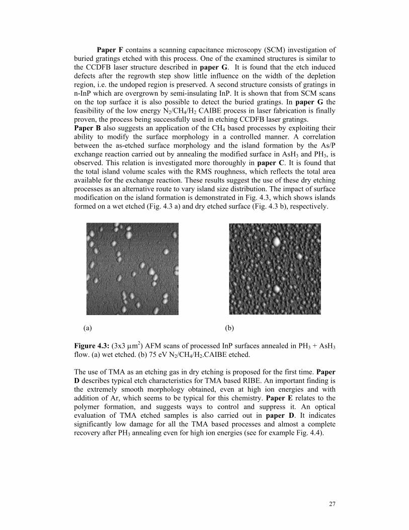
Paper F contains a scanning capacitance microscopy (SCM) investigation of buried gratings etched with this process. One of the examined structures is similar to the CCDFB laser structure described in paper G. It is found that the etch induced defects after the regrowth step show little influence on the width of the depletion region, i.e. the undoped region is preserved. A second structure consists of gratings in n-InP which are overgrown by semi-insulating InP. It is shown that from SCM scans on the top surface it is also possible to detect the buried gratings. In paper G the feasibility of the low energy N2/CH4/H2 CAIBE process in laser fabrication is finally proven, the process being successfully used in etching CCDFB laser gratings. Paper B also suggests an application of the CH4 based processes by exploiting their ability to modify the surface morphology in a controlled manner. A correlation between the as-etched surface morphology and the island formation by the As/P exchange reaction carried out by annealing the modified surface in AsH3 and PH3, is observed. This relation is investigated more thoroughly in paper C. It is found that the total island volume scales with the RMS roughness, which reflects the total area available for the exchange reaction. These results suggest the use of these dry etching processes as an alternative route to vary island size distribution. The impact of surface modification on the island formation is demonstrated in Fig. 4.3, which shows islands formed on a wet etched (Fig. 4.3 a) and dry etched surface (Fig. 4.3 b), respectively.
(a) (b) Figure 4.3: (3x3 µm2) AFM scans of processed InP surfaces annealed in PH3 + AsH3 flow. (a) wet etched. (b) 75 eV N2/CH4/H2.CAIBE etched. The use of TMA as an etching gas in dry etching is proposed for the first time. Paper D describes typical etch characteristics for TMA based RIBE. An important finding is the extremely smooth morphology obtained, even at high ion energies and with addition of Ar, which seems to be typical for this chemistry. Paper E relates to the polymer formation, and suggests ways to control and suppress it. An optical evaluation of TMA etched samples is also carried out in paper D. It indicates significantly low damage for all the TMA based processes and almost a complete recovery after PH3 annealing even for high ion energies (see for example Fig. 4.4).

28
Figure 4.4: PL intensity of near surface quantum wells as a function of the ion energy for TMA RIBE. The PL intensity is normalised with respect to wet etching for the same remnant cap layer thickness (25 nm).
In paper H, characterisation of etch induced damage for nitrogen containing
processes, such as N2 milling, TMA based RIBE and N2/CH4/H2 CAIBE, is presented. In addition to the PL evaluation method described in paper B, I-V measurements of Au/InP metal semiconductors contacts, fabricated on low doped n-InP, and SIMS measurements to monitor possible nitrogen incorporation is investigated. Further, the impact of annealing in PH3 ambient at 650 oC on these characteristics are studied. It is found from the I-V curves that the contacts made on as-etched samples are all ohmic, in contrast to the Schottky diode behaviour of the unprocessed samples. However, contacts made on annealed samples exhibit Schottky behaviour. Similarly, the PL experiments show recovery in the intensity after annealing. The SIMS data of the as-etched samples show incorporation of nitrogen for both N2 and TMA based processes, however, after annealing the nitrogen levels drop to background levels. By comparing the degree of recovery in both PL and I-V characteristics, it is found that a near complete damage removal is possible with TMA based processes.
In the last paper I, the I-V investigation on the etch-induced damage is complemented by SCM and topography studies. The very low SCM signals on n-InP samples after dry etching indicate a highly doped layer, while after annealing the SCM signal becomes appreciably high comparable to the unprocessed sample. For the nitrogen containing processes this behaviour is consistent with the I-V data in paper H. In addition, the morphology improved upon annealing: the high frequency spiky as-etched surface was transformed into a roughened step/terrace like structure. The results in paper H and paper I reveal significant reduction in the etch-induced damage upon annealing, which is attributed to stoichiometric recovery in the near surface region and possibly also to the removal of nitrogen.
Ion energy [eV]0 100 200 300 400 500 600
Nor
m. P
L in
t.
0,0
0,2
0,4
0,6
0,8
1,0
Wet etchTMA + PH3-anneal

29
5 Conclusions In summary the thesis has addressed the following issues: (i) Ion beam etching of InP using CH4 and TMA based chemistry (ii) Characterisation of etch induced damage (iii) Damage reduction by annealing under phosphine (iv) Development of a low damage process suitable for fabrication of laser gratings (v) Island formation by the As/P exchange reaction on surfaces modified by ion
beam etching. The major conclusions drawn are the following: (i) In ion beam etching using Ar/CH4/H2 and N2/CH4/H2 the N2 based processes
result in very smooth surfaces and lower polymer formation. Further, in general for these chemistries CAIBE processes produce less polymers than their RIBE counterparts.
(ii) The as-etched surface morphology correlates with the recovery/degradation of PLI of quantum wells near the surface after annealing in PH3: smooth and rough surfaces resulting in recovery and degradation of PLI, respectively. Since a hot PH3 atmosphere is typical in regrowth, these results are important for identification of etch processes suitable for application that involve etching and epitaxial regrowth.
(iii) Ion beam etching using TMA has the advantage over CH4 based processes in producing smoother surface morphology and less etch-induced damage (PLI-wise). Further, after annealing the PLI is even comparable with wet etched samples. Significantly, this is also the case at reasonably high ion energies (500 eV) and together with Ar. This allows low damage etching at higher etch rates. Polymer formation is observed for this chemistry, but it can be suppressed by addition of N2, as was also the case with the CH4 based chemistry.
(iv) I-V measurements of Au contacts made on dry-etched low n-doped InP show ohmic behaviour. However, after annealing in PH3 a Schottky behaviour similar to unprocessed samples is observed, suggesting damage removal. This is attributed to stoichiometric recovery in the near surface region. Topographic data, obtained by AFM, show a transformation in surface morphology from high frequency roughness to roughened step/terrace like features upon annealing. Further, for nitrogen containing processes (i.e. based on N2 or TMA), SIMS analysis show that incorporation of nitrogen occurs during the etch process, however, after the annealing the nitrogen level falls to background levels. SCM was also used for evaluating the etch process, but the measured regions were in the nanometer scale. These results agree with the I-V measurement. A highly doped near surface layer is observed for as-etched samples, while annealed samples show low doping. SCM is also found to be a useful tool for characterisation of regrown laser gratings. Investigation of cross sections indicates that the influence of etch induced defects on the depletion width of the p-i-n junction is small for the process used in the laser fabrication.
(v) Island formation by the As/P exchange reaction upon annealing in AsH3/PH3 is found to be extremely sensitive to the physical nature of the as-etched surface. The island formation relates to the as-etched morphology, the total island volume scaling with the RMS roughness of the as-etched surface.

30
Suggestions for future work: (1) Establish the TMA etch chemistry in other etching methods like RIE and ICP-
RIE. Such a process development can be foreseen to be of great significance for the optoelectronic industry.
(2) Further, etching of III-V compounds other than InP and possibly II-VI materials, using TMA needs to be investigated. Such studies will promote increased understanding and possibly result in an increased application range of the TMA chemistry.
(3) In-situ SIMS, rest gas analysis and optical emission experiments can be used to estimate the levels of different species in the plasma for TMA based processes. Further, by using faraday cup and pyrometer the current density of the ion beam and the substrate temperature can be measured, respectively. These parameters, together with the other process parameters, can be used to model the etch process.
(4) Extended investigation on nitridation and how it affects the electrical and optical properties, using different nitrogen containing chemistries. This could include SIMS, RBS, XPS and TEM measurements as well as annealing
experiments.

31
6 Summary of the papers
Paper A Low energy ion beam etching of InP using methane chemistry
In this paper the etch characteristics of RIBE and CAIBE using Ar/CH4/H2 and N2/CH4/H2 are investigated for different etch parameters. Major findings are the lower polymer formation and smoother surface morphology obtained for the N2 based chemistry over the Ar based chemistry, under similar conditions and in both etch modes. Further, the CAIBE processes are found to produce less polymers than their RIBE counterparts for both chemistries. Both the low energy N2 based processes show good etch characteristics, however, from a maintenance point of view the CAIBE process is superior due to the lower polymer formation in the ion-gun part.
Paper B Extremely smooth surface morphologies in N2/H2/CH4 based low energy chemically assisted ion beam etching of InP/GaInAsP
The application of N2/CH4/H2 CAIBE is investigated and the etch-induced damage is characterised by measuring the PL of near surface quantum wells and by AFM. The low energy N2/CH4/H2 CAIBE process is shown to be promising with respect to both surface morphology and PL-yield. In addition, annealing in PH3 at 650 oC (typical regrowth environment) is found to significantly enhance the PLI for this process. Further, a correlation between the as-etched surface morphology and the post-annealed PLI is observed. Drastic degradation of PLI for samples with rough surface morphology is seen and is attributed to migration of the lattice disorder deeper into the sample upon annealing. Finally, island formation on etched InP surfaces after annealing in a PH3/AsH3 mixture is found to relate to the as-etched surface morphology.
Paper C Impact of surface morphology on InAs(P) island formation on InP
This paper focus on the relation between InAs(P) island formation on InP surfaces by As/P exchange reaction and the substrate surface morphology. The substrate morphology was modified by etching in a controlled way. The island formation is found to be extremely sensitive to the physical nature of the pre-annealed surface. The determined total island volume scales with the RMS roughness of the as-etched surface morphology. This reflects the increased surface area available for the As/P exchange reaction.
32
Paper D Trimethylamine: Novel source for low damage reactive ion beam etching of InP
In this work, TMA is presented as a new methyl source for dry etching of InP. Extremely smooth etched morphologies are characteristic for the TMA processes. Furthermore, from PL evaluation of the etch induced damage, the optical quality of the etched near surface regions is found to be comparatively good for the different processes, and, upon annealing in PH3 it becomes comparable to wet etching. Significantly, these good properties are retained even at reasonably high ion energies (500 eV) and with addition of Ar. This suggests use of this chemistry in applications such as standard RIE, which has a high self-induced bias (∼500 eV).
Paper E Polymer free reactive ion beam etching of InP using N2/(CH3)3N
This work studies the influence of TMA flow and rf power on polymer formation in the TMA RIBE process developed in paper D. Polymer formation is significantly affected by TMA flow, while the rf power affects it only moderately. By optimising these two parameters the polymer formation can be minimised but not completely avoided. However, as for the CH4 based chemistry (Paper A), addition of N2 in the process is found to retard the polymer formation and the process can be made polymer free while still retaining all the good etch characteristics of the TMA process.
Paper F Doping landscapes in the nano-meter range by scanning capacitance microscopy
SCM is used to image doping variations in the nano-meter length scale. Two types of structures are investigated. The first structure consists of periodically corrugated p-i-n junctions, similar to that found in a buried heterostructure CCDFB laser, with N2/CH4/H2 CAIBE etched gratings. The second is an embedded grating structure, also formed by N2/CH4/H2 CAIBE. The gratings consist of n-doped InP, and are overgrown with semi-insulating InP. In the first case, cross section scans show that the assumed doping profile is preserved, which indicates that the doping incorporation during regrowth is not affected by the presence of gratings. Further, the depletion region is comparable with the estimated value, which suggests that the influence of etch induced defects on the depletion width is smaller than the present resolution. Examination from the top surface of the second structure reveals the buried gratings, thus demonstrating capacitive detection of subsurface nano-structures.

33
Paper G Buried heterostructure complex-coupled distributed feedback 1.55 µ m lasers fabricated using dry etching processes and quaternary layer overgrowth
A buried heterostructure complex coupled DFB laser emitting at 1.55 µm is fabricated by using the N2/CH4/H2 CAIBE process to etch the gratings, which are situated in the active region. The fabrication process also comprises GaInAsP overgrowth by MOVPE over the gratings to reduce the index coupling and promote gain coupling, as well as semi-insulating regrowth by HVPE to facilitate lateral mode confinement and thermal dissipation. The successful laser results proves that the N2/CH4/H2 CAIBE process is suitable for these kind of applications; threshold currents around 20 mA, stable single mode operation with large side mode suppression ratio (55 dB), -3 dB bandwidth of 10 GHz, and high single-mode yield for as-cleaved devices (87 %).
Paper H Characterisation of damage in InP dry-etched using nitrogen containing chemistries
Different nitrogen containing processes, such as nitrogen milling, TMA based RIBE and N2/CH4/H2 CAIBE, are investigated with respect to the etch induced damage. I-V characteristics of Au/InP metal semiconductor contacts and the PL evaluation method described in Paper B are used to quantify the residual surface damage. From the I-V measurements of the contacts on as-etch samples it is found that they all exhibit ohmic behaviour. On the other hand, while the PL yield is lower than the wet etched control sample there are also intensity variations among the different processes and these variations are attributed to hydrogen passivation of defects. SIMS measurements reveal nitrogen incorporation in the near surface region for all these processes. Annealing in a PH3 atmosphere at 650 oC has a major impact on these properties; the nitrogen levels drop to the background levels, while both significant recovery in PL and recovery to Schottky diode behaviour is observed. These trends in I-V and PL characteristics are attributed to recovery in the near surface stoichiometry and possibly due to reduction in nitrogen related defects. Finally, it is shown that a near-complete damage removal can be obtained with TMA based processes.
Paper I Scanning Capacitance Microscopy as an in-line evaluation tool for dry etching of semiconductors: A case study with InP
This work contains a SCM investigation of processed low doped n-InP samples. Dry etched samples are found to yield low SCM signals (dC/dV), which is indicative of a highly doped near surface region. After PH3 annealing high SCM signals are obtained suggesting damage removal. This observed recovery seems to correlate with the morphological improvements seen in the topographic data. The SCM results are also found to agree with I-V characteristics of (macroscopic) Au contacts made on these

34
samples. Thus, this work demonstrates the feasibility of using SCM as rapid in-line evaluation tool for dry etching of semiconductors.

35
7 List of publications not included in this thesis J. Backlund, J. Bengtsson, C.F. Carlstrom, A. Larsson “Multifunctional grating couplers for bidirectional incoupling into planar waveguides” IEEE-Photon. Technol. Lett. 12(3), (2000) 314 K. Hieke, J.O. Wesström, E. Forsberg, and C.F. Carlström., “Ballastic transport at room temperature in deeply etched cross junctions”. Semiconductor. Sci. Technol. 15, (2000) 272 J. Vukusic, J. Bengtsson, M. Ghisoni, A. Larsson, C.F. Carlstrom, and G. Landgren, “Fabrication and characterization of diffractive optical elements in InP for monolithic integration with surface-emitting components” Appl. Opt. 39(3), (2000) 398 J. Backlund, J. Bengtsson, C.F. Carlström, and A. Larsson, “Incoupling waveguide holograms for simultaneous focusing into multiple arbitrary positions” Appl. Opt. 38(27), (1999) 5738 S. Anand, D. Söderström, C.F. Carlström, S. Lourdudoss, and G. Landgren., “Investigations of p-i-n junctions with nanoscale corrugations” Inst. Phys. Conf. Ser. 164, Paper presented at Microscopy of Semiconductor Materials Conference, Oxford, UK, 22-25 Mars 1999, 629 J. Backlund, J. Bengtsson, C.F. Carlström, and A. Larsson, “Incoupling waveguide hologram with reduced polarization sensitivity” IEEE Photon. Technol. Lett., 11(2), (1999) 227 S. Anand, C.F. Carlström, G. Landgren, D. Söderström and S. Lourdudoss, “Process damage in chemically assisted ion beam etching of InP/GaInAsP” 1998 Proceeding of InP and Related Materials, Tsukuba, Japan, 175 C.F. Carlström, S. Anand, E. Niemi, and G. Landgren, “Correlation between morphology and island formation on InP surfaces” 1999 Proceeding of InP and Related Materials, Davos, Switzerland, 519


37
8 Acknowledgement There are so many people who have assisted me through these years and to whom I am indebted. If anyone is not mentioned here I beg pardon and thank him or her anyway. I would like to express my gratitude to: Prof. Gunnar Landgren for employing and supervising me during the first year. It was he who decided there should be a dry etching activity in the first place. I thank him for the support and encouragement he has always showed me. My tutor Docent Srinivasan “By the way” Anand for his knowledge and friendship. Many are the academic discussions we had and often were they both intensive and long. I wish all those ideas were made into publications. Prof. Sebastian Lourdudoss for discussions on chemistry as well as other things. It was a pleasure to work with him and David Söderström in the Nanolase project. Björn “beer brewer” Bark and Lars Matsson for helping with the machine maintenance, an indeed demanding task. Among the people who have helped me with the experimental work are Janos Andre, Mattias Dahlström, Nicky Chitica, Carl Asplund, Olivier Douheret, Dan Haga, Christiane Burgermeister, Björn Stålnacke, Amit Patel, Jan-Olof Wesström, Stefan Nilsson, Lena Bäckbom, and Tina Klinga Other professionals who also have been nice to have around for discussions: Mattias Hammar, Nils Nordell, Thomas Palm, Gunnar Andersson, Fredrik Salomonsson, Jonas Bentell, don Martin Mc Strassner, Sebastian Mogg, Egbert Rodriguez-Messmer, Margareta Linnarsson, Esko Niemi and all the others at the department. Michael “Dry etcher II” Mulot and Peter Goldman for taking over many things…. Agneta Ogden for excellently carrying out the bureaucratic stuff. To reset my brain, during free time many beers were consumed together with Dietmar “von Warsteiner” Keiper, Henrik “KWK 71” Hillborg, Rickard “gnagaren” Adermark and Patrik “Zola” Ekström. My family for all their support. A special thanks also goes to my father for his chemistry knowledge, which is not limited to alcohols but includes amines as well “Pa, do you know any low energy methyl source? –Well, how is it with those methylamines….”.

38

39
9 References 1 I. Adesida, C. Youtsey, A. T. Ping, F. Khan, L. T. Romano, and G. Bulman, “Dry and wet etching for group III nitrides”, MRS-Internet-Journal-of-Nitride-Semiconductor-Research. 4S1, (1999) 2 Y. Kaneko, N. Yamada, T. Takeuchi, Y. Yamaoka, H. Amano, and, I. Akasaki, “Melt-back etching of GaN”, Solid state Electron. 41, (1997) 295 3 S. V. Novikov, T. S. Cheng, Z. Mahmood, I. Harrison, and, C. T. Foxon, “Selective meltback etching of GaN layers in liquid-phase electroepitaxial technique”, J. Cryst. Growth 173, (1997) 1 4 M. S. Minsky, M. White, and E. L. Hu, “Room-temperature photoenhanced wet etching of GaN”, Appl. Phys. Lett. 68, (1996) 1531 5 I. Adesida, A. T. Ping, C. Youtsey, T. Dow, M. Asif-Khan, D. T. Olson, and J. N. Kuznia, “Characteristics of chemically assisted ion beam etching of gallium nitride”, Appl. Phys. Lett. 65(7), (1994) 889 6 S. A. Smith, C. A. Wolden, M. D. Bremser, A. D. Hanser, R. F. Davis, W. V. Lampert, “High rate and selective etching of GaN, AlGaN, and AlN using an inductively coupled plasma”, Appl. Phys. Lett. 25(22), (1997) 3631 7 C. B. Vartuli, S. J. Pearton, J. W. Lee, J. Hong, J. D. MacKenzie, C. R. Abernathy, and R. J. Shul, “ICl/Ar electron cyclotron resonance plasma etching of III-V nitrides”, Appl. Phys. Lett. 69(10), (1996) 1426 8 R. J. Shul, G. B. McClellan, S. A. Casalnuovo, D. J. Rieger, S. J. Pearton, C. Constantine, C. Barratt, R. F. Jr. Karlicek, C. Tran, and M. Schurman, “Inductively coupled plasma etching of GaN”, Appl. Phys. Lett. Vol. 69, no. 8 (1996) p. 1119 9 D. L. Tolliver, in “VLSI Electronics: Microstructure Science, Vol. 8 Plasma processing for VLSI”, edited by N. G. Einspruch, and D. M. Brown (Academic Press, Orlando 1984) 10 N. Grote in “Materials for optoelectronics”, edited by M. Quillec (CNET, France), Kluwer Academic publications (Boston 1996) 11 T. Baba, “Photonic Crystals and Microdisk Cavities Based on GaInAsP-InP Systems”, IEEE J. Quantum Electronics, 3(3), (1997) 1 12 H. C. Liu, “New quantum devices”, Physica E, 8(2), (2000) 170 13 H. Schweizer, U. A. Griesinger, V. Harle, F. Adler, M. Burkard, F. Barth, J. Hommel, C. Kaden, J. Kovac, J. Kuhn, B. Klepser, G. Lehr, F. Prins, F. Scholz, M. H. Pilkuhn, J. Straka, A. Forchel, and G. W. Smith, “Optoelectronic nanostructures: Physics and technology”, Proceedings-of-the-SPIE The-International-Society-for-Optical-Engineering. 2399, (1995) 407

40
14 T. R. Hayes, W. C. Dautremont-Smith, H. S. Luftman, and J. W. Lee, “Passivation of acceptors in InP resulting from CH/sub 4//H/sub 2/ reactive ion etching”, Appl. Phys. Lett. 55(1), (1989) 56 15 S. Balasubramanian, N. Balasubramanian, andV. Kumar, “Effect of hydrogenation on the photoluminescence of n-InP”, Semicond. Sci. and Technol.10(3), (1995) 310 16 L. G. Deng, M. Rahman, and C. D. W. Wilkinson, “Enhanced damage due to light in low-damage reactive ion etching processes”, Appl. Phys. Lett. 76(20), (2000) 2871 17 R. Cheung, Y. H. Lee, C. M. Knoedler, K. Y. Lee, T. P. Smith, and D. P. Kern, “Sidewall damage in n+-GaAs quantum wires from reactive ion etching”, Appl. Phys. Lett. 54(21), (1989) 2130 18 S. W. Pang, W. D. Goodhue, T. M. Lyszczarz, D. J. Ehrlich, R. B. Goodman, and G. D. Johnson, “Dry etching induced damage on vertical sidewalls of GaAs channels”, J. Vac. Sci. Technol. B6(6), (1988) 1916 19 H. F. Wong, D. L. Green, T. Y. Liu, D. G. Lishan, M. Bellis, E. Hu, P. M. Petroff, P. O. Holtz, and J. L. Merz, “Investigation of reactive ion etching induced damage in GaAs-AlGaAs quantum well structures”, J. Vac. Sci. and Technol. B 6(6), (1988) 1906 20 R. Germann, A. Forchel, and D. Grutzmacher, “Optical depth profiling of ion beam etching induced damage in InGaAs/InP heterostructures”, Appl. Phys. Lett. 55(21), (1989) 2196 21 J. E. Parmeter, R. J. Shul, A. J. Howard, and P. A. Miller, “Treatment of InP surfaces in radio frequency H2 and H2/CH4/Ar plasmas: in situ compositional analysis, etch rates, and surface roughness”, J. Vac. Sci. Technol. B 14(6), (1996) 3563 22 C. Constantine, D. Johnson, S. J. Pearton, U. K. Chakrabarti, A. B. Emerson, W. S. Hobson, and A. P. Kinsella, “Plasma etching of III-V semiconductors in CH/sub 4//H/sub 2//Ar electron cyclotron resonance discharges”, J. Vac. Sci. Technol. B 8(4), (1990) 596 23 S. J. Pearton-SJ, U. K. Chakrabarti, A. P. Perley, and K. S. Jones, “Ion milling damage in InP and GaAs”, J. Appl. Phys. 68(6), (1990) 2760 24 M. G. Dowsett, R. M. King, and E. H. C. Parker, “SIMS evaluation of contamination on ion-cleaned (100) InP substrates”, Appl. Phys. Lett. 31(8), (1977) 529 25 X. Li, T. A. Gessert, and T. J. Coutts, “Near-surface type conversion of p-type single-crystal InP by plasma exposure”, AIP-Conf. Proc. 227, (1991) 126 26 W. C. Dautremont-Smith, P. A. Barnes, and J. W. Jr. Stayt, “A nonalloyed, low specific resistance Ohmic contact to n-InP”, J. Vac. Sci. Technol. B 2(4), (1984) 620

41
27 U. Niggebrugge, M. Klug, and G. Garus, “A novel process for reactive ion etching on InP, using CH4/H2”, Gallium Arsenide and Related Compounds 1985. Proceedings of the Twelfth International Symposium. Adam Hilger, Bristol, UK, xix+759, (1986) 367 28 Coburn and Winters, “Ion- and electron-assisted gas-surface chemistry-an important effect in plasma etching”, J. Appl. Phys. 50, (1979) 3189 29 Wei-Hsiu-Hung, Jyh-Tsung-Hsieh, Huey-Liang-Hwang, Hsin-Yen-Hwang, and Che-Chen-Chang, “Surface etching of InP(100) by chlorine”, Surface Sci. 418(1), (1998) 46 30 C. Constantine, C. Barratt, S. J. Pearton, F. Ren, and J. R. Lothian, “Microwave Cl/sub 2//H/sub 2/ discharges for high rate etching of InP”, Electron. Lett. 28(18), (1992) 1749 31 T. Yoshikawa, S. Kohmoto, M. Anan, N. Hamao, M. Baba, N. Takado, Y. Sugimoto, M. Sugimoto, K. Asakawa, “Chlorine-based smooth reactive ion beam etching of indium-containing III-V compound semiconductor”, Jpn. J. Appl. Phys. Part. 1, 31(12B), (1992) 4381 32 Y. Feurprier, Ch. Cardinaud, and G. Turban, “X-ray photoelectron spectroscopy damage characterization of reactively ion etched InP in CH4/H2 plasmas”, J. Vac. Sci. Technol. B 16(4), (1998) 1823 33 V. J. Minkiewicz , and B. N. Chapman, “Triode plasma etching”, Appl. Phys. Lett. 34, (1979) 192 34 D. L. Pappas, and J. Hopwood, “Deposition of diamond like carbon using planar radio frequency induction plasma”, J. Vac. Sci. Technol. A12(4), (1994) 1576 35 W. Dworschak, R. Kleber, A. Fuchs, B. Scheppat, G. Keller, K. Jungh, abd H. Ehrhardt, “Polymer like and hard amorphous hydrogenated carbon films prepared in an inductively coupled RF glow discharge”, Thin Solid Films 189(2), (1990) 257 36 H. R. Kaufman, in “Advances in Electronics and Electron Physics”, edited by L. Marton (Academic, New York, 1974), Vol. 36, 265 37 H. R. Kaufman, J. J. Cuomo, and J. M. E. Harper, “Technology and applications of broad beam ion sources used in sputtering. Part I. Ion Source Technology”, J. Vac. Sci. Technol. 21(3), (1982) 725 38 G. Aston, H. R. Kaufman, and P. J. Wilbur, “Ion Beam Divergence Characteristics of Two-Grid Accelerator Systems”, AIAA Journal, 16(5), (1978) 516 39 W. Katzchner, U. Niggebrugge, R. Löffler, and H. Schröter-Janssen, “Reactive ion beam etching of InP with N2 and N2/O2 mixtures”, Appl. Phys. Lett. 48(3), (1986) 230 40 F. Frost, A. Schindler, and F. Bigl, “Ion beam smoothing of indium-containing III-V compound semiconductors”, Appl. Phys. A 66, (1998) 663

42
41 W. Katzchner, A. Steckenborn, R. Löffler, and N. Grote, “Ion beam milling of InP with an Ar/O2-gas mixture”, Appl. Phys. Lett. 44(3), (1984) 352 42 S. C. McNevin, “Chemical etching of GaAs and InP by chlorine: the thermodynamically predicted dependence on Cl2 pressure and temperature”, J. Vac. Sci. Technol. B4(5), (1986) 1216 43 R. Panepucci, C. Youtsey, D. A. Turnbull, S. Q. Gu, C. Caneau, S. G. Bishop, and I. Adesida, “Fabrication of InP/InGaAs quantum wires by free Cl2”, J. Vac. Sci. Technol. B13(6), (1995), 2752 44 Youtsey, R. Grundbacher, R. Panepucci, and I. Adesida, “Characterization of chemically assisted ion beam etching of InP”, J. Vac. Sci. Technol. B12(6), (1994) 3317 45 B. Lamontage, J. Stapledon, P. Chow-Chong, M. Buchanan, J. Fraser, J. Phillips, and M. Davies, “InP etching using chemically assisted ion beam etching (Cl2/Ar). Formation of InClx clusters under high concentration of chlorine”, J. Electrochem. Soc. 146(5), (1999) 1918 46 M. Vernon, T. R. Hayes, and V. M. Donnelly, “Intrinsic mechanisms of smooth and rough morphology in etching of InP by Cl2 determined by infrared laser interferometry”, J. Vac. Sci. Technol. A10, (1992) 3499 47 J. Lee, J. Hong, and S. J. Pearton, “Etching of InP at >1 µm/min in Cl2/Ar plasma chemistries”, Appl. Phys. Lett. 68(6), (1996) 847 48 L. M. Bharadwaj, P. Bonhomme, J. Faure, G. Balossier, and R. P. Bajpai, “Chemically assisted ion beam etching on InP and InSb using reactive flux of iodine and Ar+ beam”, J. Vac. Sci. Technol. B9(3), (1991) 1440 49 S. J. Pearton, U. K. Chakrabarti, A. Katz, R. Ren, and T. R. Fullowan, “High-rate, anisotropic dry etching of InP in HI-based discharges”, Appl. Phys. Lett. 60(7), (1992) 838 50 S. Oku, Y. Shibata, and K. Ochiai, “Controlled beam dry etching of InP by using Br2-N2 gas”, 1995 Proceedings of InP and Related Materials, New York, USA, 561 51 D.L. Melville, J.G. Simmons, and D. A. Thompson, “Identification of volatile products in low pressure hydrocarbon electron cyclotron resonance reactive ion etching of InP and GaAs”, J. Vac. Sci. Technol. B11(6), (1993) 2038 52 Y. Feurprier, C. Cardinaud, B. Grolleau, and G. Turban, “Etch product identification during CH4-H2 RIE of InP using mass spectrometry”, Plasma-Sources, - Science and -Technology. 6(4), (1997) 561 53 H. Schmid,.” Plasma mass spectrometric analysis and control of reactive ion etching of InP and related compounds”, 1987 Proceeding of 6th International Conference on Ion and Plasma-assisted techniques, Brighton (UK), 98 54 T. R. Hayes, M. A. Dreisbach, P. M. Thomas, W. C. Dautremont-Smith, and

43
L. A. Heimbrook, “Reactive ion etching of InP using CH4/H2 mixtures: mechanisms of etching and anisotropy”, J. Vac. Sci. Technol. B7(5), (1989) 1130 55 Z. Lj. Petrovic, B. Boskovic, A. Jelenak, and B. Tomcik, “Axial distribution of emission and rate of deposition of diamond-like film in r.f. discharges in CH4”, Thin Solid Films, 304, (1997) 136 56 E. Goglides, C. Buteau, A. Rhallabi, and G. Turban, “Radio-frequency glow discharges in methane gas: modelling of the gas-phase physics and chemistry”, J. Phys. D. Appl. Phys. 27, (1994) 818 57 S. Motlagh, and J. J. Moore, “Cross sections for radicals from electron impact on methane and fluoroalkanes”, J. Chem. Phys. 109(2), (1998) 432 58 D. J. Dagel, C. M. Mallouris, and J. R. Doyle, “Radical and film growth kinetics in methane radio-frequency glow discharges”, J. Appl. Phys. 79 (11), (1996) 8735 59 M. Kareev, M. Sablier, and T. Fujii, “Diagnosis of a CH4/N2 microwave discharge: ionic and neutral species”, J. Phys. Chem. A104(31), (2000) 7218 60 P. Pecher, and W. Jacob, “Determination of the absolute CH3 radical flux emanating from a methane electron cyclotron resonance plasma”, Appl. Phys. Lett. 73(1), (1998) 31 61 H. Kojima, H. Toyoda, and H. Sugai, “Observation of CH2 radical and comparison with CH3 radical in a RF methane discharge”, Appl. Phys. Lett. 55(13), (1989) 1292 62 H. Sugai, H. Kojima, A. Ishida, and H. Toyoda, “Spatial distribution of CH3 and CH2 radicals in a methane RF discharge”, Appl. Phys. Lett. 56(26), (1990) 2616 63 D. A. Doughty, and A. Gallagher, “Spatial distribution of a-Si:H film-producing radicals in silane RF glow discharges”, J. Appl. Phys. 67, (1990) 139 64 J. A. Doyle, D. A. Doughty, and A. Gallagher, “Plasma chemistry in silane/germane and disilane/germane mixtures”, J. Appl. Phys. 71, (1992) 4727 65 D. A. Doughty, and A. Gallagher, “Causes of SiH4 dissociation in silane DC discharges”, Phys. Rev. A 42, (1990) 6166 66 J. E. Spencer, T. R. Schimert, J. H. Dinan, D. Endres, and T. R. Hayes, “Methyl radical etching of compound semiconductors with a secondary afterglow reactor”, J. Vac. Sci. Technol. A8(3), (1990) 1690 67 A. Rhallabi, L. Houlet, and G. Turban, “Estimation of surface kinetic parameters and two-dimensional simulation of InP pattern features during CH4-H2 plasma etching”, J. Vac. Sci. Technol. B18(4), (2000) 1366 68 L. Houlet, A. Rhallabi, and G. Turban, Microscopic modelling of InP etching in CH4-H2 plasma, J. Vac. Sci. Technol. A17(5), (1999) 2598 69 T. R. Hayes, in “Indium Phosphide and Related Materials: Processing Technology and Devices”, edited by A. Katz (Artech House, Boston 1992)

44
70 L. Henry, C. Vaudry, and Granjoux, “Novel process for integration of optoelectronic devices using reactive ion etching without chlorinated gas”, Electron Lett. 23, (1987) 1254 71 S. J. Pearton, J. W. Lee, E. S. Lambers, C. R. Abernathy, F. Ren, W. S. Hobson, and R. J. Shul, “Comparison of dry etching techniques for III-V semiconductors in CH4/H2/Ar plasmas”, J. Elec. Chem. Soc. 143(2), (1996) 752 72 Y. Feurprier, Ch. Cardinaud, and G. Turban, “Influence of the gas mixture on the reactive ion etching of InP in CH4-H2 plasmas”, J. Vac. Sci. Technol. B15(5), (1997) 1733 73 O. Wada, “Ar ion-beam etching characteristics and damage production in InP”, J. Phys. D 17(12), (1984) 2429 74 N. Bouadma, P. Devoldere, B. Jusserand, P. Ossart, “Ion beam etching and surface characterization of indium phosphide”, Appl. Phys. Lett. 48(19), (1986) 1285 75 A. von Keudell, T. Schwarz-Selingere, M. Meier, and W. Jacob, “Direct identification of the synergism between methyl radicals and atomic hydrogen during growth of amorphous hydrogenated carbon films”, Appl. Phys. Lett. 76(6), (2000) 676 76 N. V. Mantzaris, E. Gogolides, A. G. Boudouvis, A. Rhallabi, and G. Turban, “Surface and plasma simulation of deposition processes: CH4 plasmas for the growth of diamond-like carbon”, J. Appl. Phys. 79(7), (1996) 3718 77 D. J. Dagel, C. M. Mallouris, and J. R. Doyle, “Radical and film growth kinetics in methane radio-frequency glow discharges”, J. Appl. Phys. 79(11), (1996) 8735 78 K. Tachibana, M. Nishida, H. Harima, and Y. Urano, “Diagnostic and modelling of a methane plasma used in the chemical vapour deposition of amorphous carbon films”, J. Phys. D: Appl. Phys. 17, (1984) 1727 79 E. H. A. Dekenkempeneer, J. Smeets, J. Meneve, L. Eersels, and R. Jacobs, “Plasma processes in methane discharges during RF plasma-assisted chemical vapour deposition of a-C:H thin films”, Thin Solid Films, 241, (1994) 269 80 C. Haag, and H. Suhr, “Etching of metals by means of organic radicals”, Plasma Chem. and Plasma Processing, 6(3), (1986) 197 81 Z. Li. Petrovic, B. Boskovic, A. Jelenak, and B. Tomcik, “Axial distribution of emission and rate of depostion of diamond like film in RF discharges in CH4” Thin Solid Films 304, (1997) 136 82 J. R. Sendra, and J. Anguita, “Reactive ion beam etching of indium phosphide in electron cyclotron resonance plasma using methane/hydrogen/nitrogen mixtures”, Jpn. J. Appl. Phys., Part 2, 33(3), (1994) L390

45
83 R. C. Keller, M. Eggebert-Seelmann, and H. J. Richter, “Dry etching of Hg1-xCdxTe using CH4/H2/Ar/N electron cyclotron resonance plasmas”, J. Electronic Materials. 25(8), (1996) 1270 84 J. Etrillard, F. Heliot, P. Ossart, M. Juhel, G. Patriarche, P. Carcenac, C. Vieu, M. Puech, and P. Maquin, “Sidewall and surface induced damage comparison between reactive ion etching and inductive plasma etching of InP using a CH4/H2/O2 gas mixture”, J. Vac. Sci. and Technol. A 14(3), (1996) 1056 85 T. Matsui, H. Sugimoto, T. Ohishi, H. Ogata, “Reactive ion etching of III-V compounds using C2H6/H2”, Electron. Lett. 24(13), (1988) 798 86 S. J. Pearton, W. S. Hobson, F. A. Baiocchi, A. B. Emerson, and K. S. Jones, “Reactive ion etching of InP, InGaAs, InAlAs: comparison of C2H6/H2 with CCl2F2/O2”, J. Vac. Sci. Technol. B 8(1), (1990) 57 87 G. Franz, “Reactive ion etching of III/V semiconductors using carbon-containing gases. A comprehensive statistical approach”, J. Electrochem. Soc. 137(9), (1990) 2896 88 I. Deac, V. Almasan, N. Palibroda, E. Indrea, X. Filip, and I. Ursu, “A low energy source for production of CH3, CN and other free radicals: IRMPD of di- and trimethylamine molecules”, Appl. Surf. Sci. 106, (1996) 223 89 A. Chung-Phillips, and J. W. H. Kao, “Quantum chemical calculations of bonded and nonbonded interactions in saturated hydrocarbons, amines, alcohols, and ethers”, J. Chem. Phys. 71, (1979) 3514 90 S. J. Pearton, and U. K. Chakrabarti, in “Indium Phosphide and Related Materials: Processing Technology and Devices”, edited by A. Katz, (Artech House, Boston 1992) 91 J. M. Rossler, Y. Royter, D. E. Mull, W. D. Goodhue, and C. G. Fonstad, “Bromine ion-beam-assisted etching of InP and GaAs”, J. Vac. Sci. Technol. B16(3), (1998) 1012 92 Iber, S. Mo, E. Peiner, G. Vollrath, A. Schlachetzki, and F. Fiedler, “Characterization of surface damage in dry-etched InP”, Semicond, Sci. Technol. 12, (1997) 755 93 L. A. Coldren, and J. A. Rentschler, “Directional reactive-ion-etching of InP with C2 containing gases”, J. Vac. Sci. Technol. 19(2), (1981) 225 94 S. J. Pearton, U. K. Chakrabarti, A. Katz, A. P. Perley, W. S. Hobson, and C. Constantine, “Comparison of CH4/H2/Ar reactive ion etching and electron cyclotron resonance plasma etching of In-based III-V alloys”, J. Vac. Sci. Technol. B9(3), (1991) 1421 95T. Nishibe, and Shin-ya-Nunoue, “Dry etching of InGaAsP/InP structures by reactive ion beam etching using chlorine and argon”, Jap. J. Appl. Phys. Part 2, 29(12), (1990) L2449

46
96 C. S. Whelan, T. E. Kazior, and K. Y. Hur, “ High rate CH4/H2 plasma etch processes for InP”, J. Vac. Sci. Technol. B15(5), (1997) 1728 97 S. W. Pang, and K. K. Ko, “Comparison between etching in Cl2 and BCl3 for compound semiconductors using a multipolar electron cyclotron resonance source”, J. Vac. Sci. Technol. B10(6), (1992) 2703 98 S. Miyakuni, R. Hattori, K. Sato, H. Takano, and O. Ishihara, “Low ion energy electron cyclotron resonance etching of InP using a Cl2/N2 mixture”, J. Appl Phys. 78 (9), (1995) 5734 99 R. J. Shul, G. B. McClellan, R. D. Briggs, D. J. Rieger, S. J. Pearton, C. R. Abernathy, J. W. Lee, C. Constantine, and C. Barratt, “High-density plasma etching of compound semiconductors”, J. Vac. Sci. Technol. B15(3), (1997) 633 100 J. A. Diniz, J. W. Swart, K. B. Jung, J. Hong, and S. J. Pearton, “Inductively coupled plasma etching of In-based compound semiconductors in CH4/H2/Ar”, Solid State Electronics, 42(11), (1998) 1947 101 J. Etrillard, P. Ossart, G. Patriarche, M. Juhel, J. F. Bresse, and C. Dauet, “Anisotropic etching of InP with low sidewall and surface induced damage in inductively coupled plasma etching using SiCl4”, J. Vac. Sci. Technol. B15(3), (1997) 626 102 D. C. Flanders, L. D. Pressman, and G. Pinelli, “Reactive ion etching of indium compounds using iodine containing plasmas”, J. Vac. Sci. Technol. B8(6), (1990) 1990 103 H. F. Wong, D. L. Green, T. Y. Liu, D. G. Lishan, M. Bellis, E. L. Hu, P. M. Petroff, P. O. Holtz, and J. L. Merz, “Investigation of reactive ion etching induced damage in GaAs-AlGaAs quantum well structures”, J. Vac. Sci. Technol. B6(6), (1988) 1906 104 R. Germann, A. Forchel, M. Bresch, and H. P. Meier, “Energy dependence and depth distribution of dry etching-induced damage in III/V semiconductor heterostructures“, J. Vac. Sci. Technol. B7(6), (1989) 1475 105 Y. Chang, I. H. Tan, Y. H. Zhang, D. Bimberg, J. Merz, and E. Hu, “Reduced quantum efficiency of a near-surface quantum well”, J. Appl. Phys. 74, (1993) 5144 106 J. M. Moison, K. Elcess, F. Houzay, J. Y. Marzin, J. M. Gerard, F. Barthe, and M. Bensoussan, “Near-surface GaAs/Ga/sub 0.7/Al/sub 0.3/As quantum wells: interaction with the surface states”, Phys. Rev. B41, (1990) 12945 107 111 A.C. Diebold, M.R. Kump, J.J. Kopanski, D.G. Seiler "Characterization of two-dimensional dopant profiles: Status and Review" J. Vac. Sci. Technol. B14(1), (1996) 196. 108 Digital Instruments Scanning Capacitance Microscopy (SCM) Support Note No. 224, Rev. C

47
109 Y. Suzuki, H. Kumano, W. Tomota, N. Sanada, and Y. Fukuda, “Nitridation of an InP (001) surface by nitrogen ion beams”, Appl. Surf. Sci.162-163, (2000) 172 110 F. Ren, S. J. Pearton, J. R. Lothian, S. N. G. Chu, W. K. Chu, R. G. Wilson, C. R. Abernathy, and S. S. Pei, “Low resistance ohmic contacts on nitrogen ion bombarded InP”, Appl. Phys. Lett. 65(17), (1994) 2165 111 W. G. Bi, and C. W. Tu, “N incorporation in InP and bandgap bowing of InNxP1-
x”, J. Appl. Phys. 80(3), (1996) 1934


![Reactive ion etching. Material selectivity Ion Beam milling @INESC Nordiko 3000 IBD system Etch rates [Å/min] @ 70ºpan 65 W130 W * junctions, spin valves.](https://static.fdocuments.in/doc/165x107/56649d575503460f94a3545a/reactive-ion-etching-material-selectivity-ion-beam-milling-inesc-nordiko.jpg)