I/O Interfacing Slides-4 -...
17
Transcript of I/O Interfacing Slides-4 -...


8085 interfacing with I/O Devices
*
Microprocessor need to Identify I/O devices with binary number.
IO devices can be interfaced:
●Memory-Mapped I/O (using addresses from memory space)
● Device is identified by 16-bit address (Space ranges from 0000H –
FFFFH
●Standard I/O mapped or isolated I/O mapping /Peripheral Mapped I/O
has separate numbering scheme for I/O devices
● Instructions IN/OUT are used for data transfer
● Device is identified by 8-bit address (Space ranges from 00H –FFH)

*
Memory Mapping Vs Peripheral
I/O

*
Peripheral I/O Instructions
Instruction IN (code DB) inputs data from an input device into accumulator.
Opcode Operand Description IN 8-bit Port address 2-byte instruction with hexadecimal
instruction DB and second byte is port
number of input device.
Memory Machine Code Mnemonics
Address 2065 DB IN 84
2066 84
Instruction OUT (code D3) sends the content of the accumulator to output
device such as LED display.
Opcode Operand Description OUT 8-bit Port address 2-byte instruction with hexadecimal
instruction D3 and Second byte is port
number of output device.
Memory Machine Code Mnemonics
Address 2050 D3 OUT 01
2051 01

*
OUT Instruction (Machine Cycles)

*
OUT Instruction
● In First Machine cycle M1(Opcode Fetch), microprocessor places the 16-bit memory
address from the program counter (PC) on the address bus. At T1 20H is placed on A15-
A8 and 50H is placed on AD7-AD0. ALE goes high, IO/M’ goes low indicates memory
related operations. ALE indicates the availability of the address on AD7-AD0. At T2
microprocessor sends RD’ control signal which is combined with IO/M’ to generate
MEMR’ signal and processor fetches the instruction code D3 using data bus.
● M2 (memory Read), 8085 places next address 2051H on address bus and get device
address 01H.
● M3 (I/O write), 8085 place device address 01H on low and high address bus
both.IO/M’ goes high to indicate I/O operation. At T2 AC contents are placed on data bus
followed by control signal WR’. If we connect data bus to latch we can catch the
information and display on LEDs and Printer. By ANDing IO/M’ and WR’ signals IOW’
signal enable output device.
Information necessary for interfacing output device is available during T2 and T3
of
the M3 cycle.

*
IN Instruction
*
IN Instruction
● In First Machine cycle M1 (Opcode Fetch), microprocessor places the 16-bit
memory address from the program counter (PC) on the address bus. At T1 20H
is placed on A15-A8 and 65H is placed on AD7-AD0. ALE goes high, IO/M’
goes low indicates memory related operations. ALE indicates the availability of
the address on AD7-AD0. At T2 microprocessor sends RD’ control signal which
is combined with IO/M’ to generate MEMR’ signal and processor fetches the
instruction code DB using data bus.
● M2 (Memory Read), 8085 places next address 2066H on address bus and get
device address 84H.
● M3 (Memory Read), 8085 place device address 84H on low and high address
bus both and asserts RD’ signal. IO/M’ goes high to indicate IO operation. At T2
data from input port are paced on data bus and transferred to AC. By ANDing
IO/M’ and WR’ signals IOR’ signal to enable input port.

*
Data Transfer
For data transfer from input device to processor the following operations
are performed.
●The input device will load the data to the port.
●When the port receives a data, it sends message to the processor to read the
data.
●The processor will read the data from the port.
●After a data have been read by the processor the input device will load the
next data into the port.
For data transfer from processor to output device the following operations
are performed.
●The processor will load the data to the port.
●The port will send a message to the output device to read the data.
●The output device will read the data from the port.
●After the data have been read by the output device the processor can load the
next data to the port.

Device Selection and Data
Transfer Steps are summarized as:
●Decode the address bus to generate unique pulse corresponding to device address on
the bus called device address bus or I/O address pulse.
●Combine the device address pulse with the control signal to generate a device select
pulse(I/O select) that is generated only when both signals are asserted.
●Use the I/O select pulse to activate interfacing device(I/O port).
Figure: Block Diagram of IO interface
*
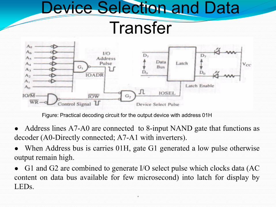
Device Selection and Data
Transfer
Figure: Practical decoding circuit for the output device with address 01H
● Address lines A7-A0 are connected to 8-input NAND gate that functions as
decoder (A0-Directly connected; A7-A1 with inverters).
● When Address bus is carries 01H, gate G1 generated a low pulse otherwise
output remain high.
● G1 and G2 are combined to generate I/O select pulse which clocks data (AC
content on data bus available for few microsecond) into latch for display by
LEDs.
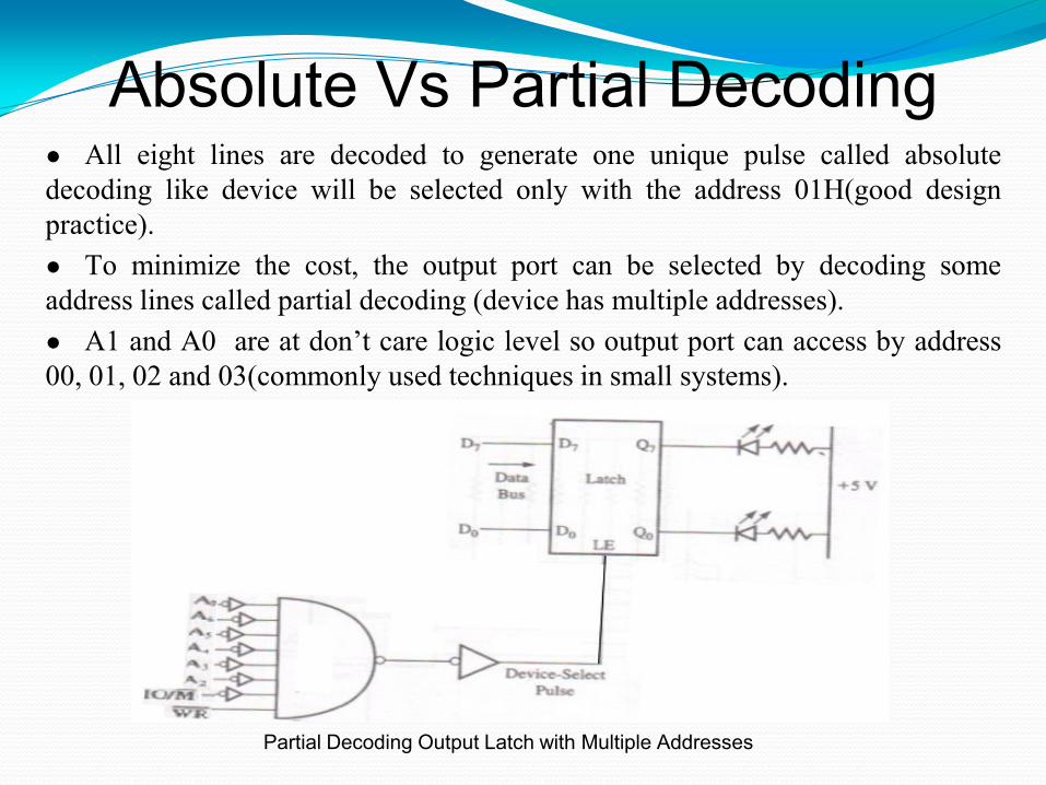
Absolute Vs Partial Decoding ● All eight lines are decoded to generate one unique pulse called absolute
decoding like device will be selected only with the address 01H(good design
practice).
● To minimize the cost, the output port can be selected by decoding some
address lines called partial decoding (device has multiple addresses).
● A1 and A0 are at don’t care logic level so output port can access by address
00, 01, 02 and 03(commonly used techniques in small systems).
Partial Decoding Output Latch with Multiple Addresses

Input Interfacing Decode logic for a Dip-Switch Input Port
● Address lines are high(FFH), output of NAND gate goes low which is
combined by control signal IOR’ which generates Device Select Pulse.
● Device select pulse enable Tri-state Buffer (used as interfacing port).
Data flow from keys to the AC.
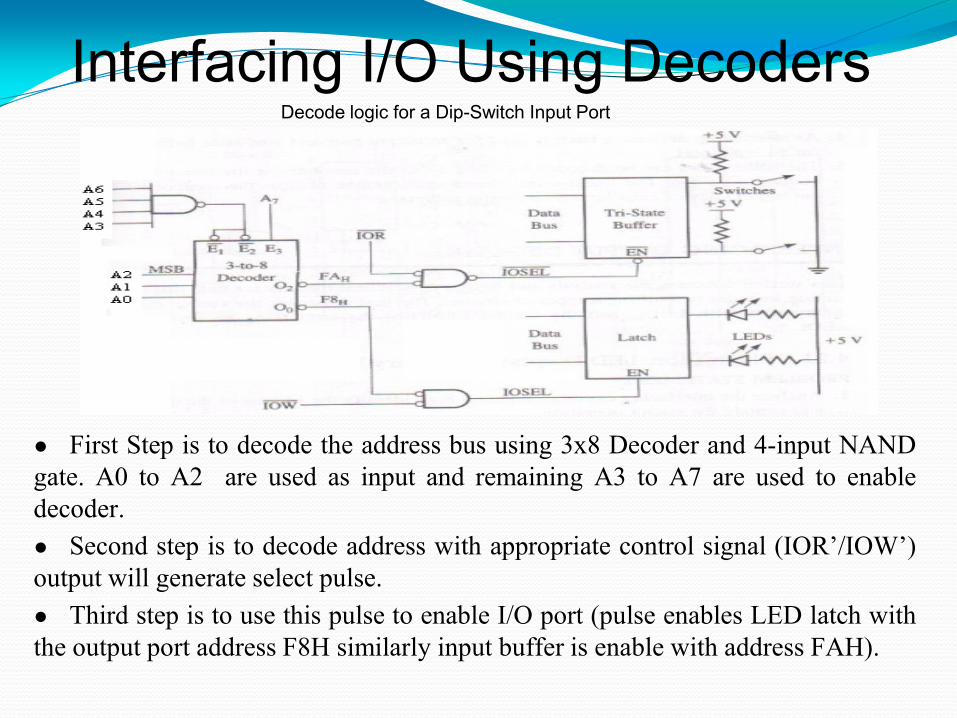
Interfacing I/O Using Decoders Decode logic for a Dip-Switch Input Port
● First Step is to decode the address bus using 3x8 Decoder and 4-input NAND
gate. A0 to A2 are used as input and remaining A3 to A7 are used to enable
decoder.
● Second step is to decode address with appropriate control signal (IOR’/IOW’)
output will generate select pulse.
● Third step is to use this pulse to enable I/O port (pulse enables LED latch with
the output port address F8H similarly input buffer is enable with address FAH).
Memory Mapped I/O
● Instead of using 8-bit address, the full 16-bits of
the address bus must be used.
● Instead of using IORD and IOWR, use MEMR
and MEMW.
● To transfer data Memory Related Instructions
such as LDA(Load AC Direct transfers data from
memory to Accumulator), STA (Store contents of
AC into Memory)are used.
● IN STA 8000H output device instead of a
memory Register is connected to the address, so
that accumulator contents will be transferred to
output device.

Memory Mapped I/O ● IN LDA 8000H accumulator receives data from input
device rather than Memory.
Execution of Memory Related data Transfer Instruction STA 8000H

THANK
YOU...