
INVITED PAPER DigitalCircuitDesign ChallengesandOpportunities...
23
INVITED PAPER Digital Circuit Design Challenges and Opportunities in the Era of Nanoscale CMOS Small transistors necessitate big changes, in the way digital circuits are modeled and optimized for manufacturability, and new strategies for logic, memory, clocking and power distribution. By Benton H. Calhoun, Member IEEE , Yu Cao, Member IEEE , Xin Li, Member IEEE , Ken Mai, Member IEEE , Lawrence T. Pileggi, Fellow IEEE , Rob A. Rutenbar, Fellow IEEE , and Kenneth L. Shepard, Senior Member IEEE ABSTRACT | Well-designed circuits are one key Binsulating[ layer between the increasingly unruly behavior of scaled complementary metal–oxide–semiconductor devices and the systems we seek to construct from them. As we move forward into the nanoscale regime, circuit design is burdened to Bhide[ more of the problems intrinsic to deeply scaled devices. How this is being accomplished is the subject of this paper. We discuss new techniques for logic circuits and interconnect, for memory, and for clock and power distribution. We survey work to build accurate simulation models for nanoscale devices. We discuss the unique problems posed by nanoscale lithography and the role of geometrically regular circuits as one promising solution. Finally, we look at recent computer-aided design efforts in modeling, analysis, and optimization for nanoscale designs with ever increasing amounts of statistical variation. KEYWORDS | Clock distribution; complementary metal–oxide– semiconductor (CMOS); device scaling; digital circuits; lithog- raphy; logic; manufacturability; memory; optimization; power distribution; regular circuit fabrics; statistical variability; yield I. INTRODUCTION For four decades, Moore’s law [1] has driven the worldwide semiconductor industry. The expectation of continued device scaling drove fundamental research on physics, materials, devices, interconnect, andVof princi- pal interest in this paperVintegrated circuits, leading to an enormous and diverse range of commercial electronics. As we move into the era of nanoscale devices, however, scaling-as-usual is under significant duress. The problems are, of course, well known. As we move to more atomistic dimensions, simple scaling eventually stops. The devices are smaller, but many aspects of their perform- ance deteriorate: leakage increases, gain decreases, and sensitivity to unavoidable small fluctuations in the manu- facturing process rises dramatically. Power and energy have become the key limiters on many new designs. We can no longer rely on experience with a few Bworst case[ process corners to predict worst case behavior for these technolo- gies. Nothing is deterministic any longer: most relevant parameters are statistical; many exhibit complex correlations and distressingly wide variances. The rising costs associated with fabricating circuits in such scaled technologies (e.g., mask costs) only exacerbate these problems of predictability. Nevertheless, we see significant opportunities in these challenges. Our goal in this paper is to survey briefly how circuit design is both affected by, and successfully re- sponding to, these challenges. In a very real sense, well- designed circuits are one key Binsulating[ layer between the increasingly unruly and nonideal behavior of scaled devices and the systems we seek to construct from them. As we move forward into the nanoscale regime, further into the (rather ominously denoted) Bend of the roadmap[ Manuscript received February 2, 2007; revised August 17, 2007. This work was supported in part by the Center for Circuit and System Solutions under the Focus Center Research Program. B. H. Calhoun is with the Department of Electrical and Computer Engineering, University of Virginia, Charlottesville, VA 22904 USA (e-mail: [email protected]). Y. Cao is with the Department of Electrical Engineering, Arizona State University, Tempe, AZ 85287 USA (e-mail: [email protected]). X. Li, K. Mai, L. T. Pileggi, and R. A. Rutenbar are with the Department of Electrical and Computer Engineering, Carnegie–Mellon University, Pittsburgh, PA 15213 USA (e-mail: [email protected]; [email protected]; [email protected]; [email protected]). K. L. Shepard is with the Department of Electrical Engineering, Columbia University, New York, NY 10027 USA (e-mail: [email protected]). Digital Object Identifier: 10.1109/JPROC.2007.911072 Vol. 96, No. 2, February 2008 | Proceedings of the IEEE 343 0018-9219/$25.00 Ó2007 IEEE
-
Upload
nguyennguyet -
Category
Documents
-
view
215 -
download
0
Transcript of INVITED PAPER DigitalCircuitDesign ChallengesandOpportunities...

INV ITEDP A P E R
Digital Circuit DesignChallenges and Opportunitiesin the Era of Nanoscale CMOSSmall transistors necessitate big changes, in the way digital circuits are
modeled and optimized for manufacturability, and new strategies
for logic, memory, clocking and power distribution.
By Benton H. Calhoun, Member IEEE, Yu Cao, Member IEEE,
Xin Li, Member IEEE, Ken Mai, Member IEEE, Lawrence T. Pileggi, Fellow IEEE,
Rob A. Rutenbar, Fellow IEEE, and Kenneth L. Shepard, Senior Member IEEE
ABSTRACT | Well-designed circuits are one key Binsulating[
layer between the increasingly unruly behavior of scaled
complementary metal–oxide–semiconductor devices and the
systems we seek to construct from them. As we move forward
into the nanoscale regime, circuit design is burdened to Bhide[
more of the problems intrinsic to deeply scaled devices. How
this is being accomplished is the subject of this paper. We
discuss new techniques for logic circuits and interconnect, for
memory, and for clock and power distribution. We survey work
to build accurate simulation models for nanoscale devices. We
discuss the unique problems posed by nanoscale lithography
and the role of geometrically regular circuits as one promising
solution. Finally, we look at recent computer-aided design
efforts in modeling, analysis, and optimization for nanoscale
designs with ever increasing amounts of statistical variation.
KEYWORDS | Clock distribution; complementary metal–oxide–
semiconductor (CMOS); device scaling; digital circuits; lithog-
raphy; logic; manufacturability; memory; optimization; power
distribution; regular circuit fabrics; statistical variability; yield
I . INTRODUCTION
For four decades, Moore’s law [1] has driven the
worldwide semiconductor industry. The expectation of
continued device scaling drove fundamental research on
physics, materials, devices, interconnect, andVof princi-
pal interest in this paperVintegrated circuits, leading to
an enormous and diverse range of commercial electronics.
As we move into the era of nanoscale devices, however,
scaling-as-usual is under significant duress.The problems are, of course, well known. As we move to
more atomistic dimensions, simple scaling eventually stops.
The devices are smaller, but many aspects of their perform-
ance deteriorate: leakage increases, gain decreases, and
sensitivity to unavoidable small fluctuations in the manu-
facturing process rises dramatically. Power and energy have
become the key limiters on many new designs. We can no
longer rely on experience with a few Bworst case[ processcorners to predict worst case behavior for these technolo-
gies. Nothing is deterministic any longer: most relevant
parameters are statistical; many exhibit complex correlations
and distressingly wide variances. The rising costs associated
with fabricating circuits in such scaled technologies (e.g.,
mask costs) only exacerbate these problems of predictability.
Nevertheless, we see significant opportunities in these
challenges. Our goal in this paper is to survey briefly howcircuit design is both affected by, and successfully re-
sponding to, these challenges. In a very real sense, well-
designed circuits are one key Binsulating[ layer between
the increasingly unruly and nonideal behavior of scaled
devices and the systems we seek to construct from them.
As we move forward into the nanoscale regime, further
into the (rather ominously denoted) Bend of the roadmap[
Manuscript received February 2, 2007; revised August 17, 2007. This work was
supported in part by the Center for Circuit and System Solutions under the Focus
Center Research Program.
B. H. Calhoun is with the Department of Electrical and Computer Engineering,
University of Virginia, Charlottesville, VA 22904 USA (e-mail: [email protected]).
Y. Cao is with the Department of Electrical Engineering, Arizona State University,
Tempe, AZ 85287 USA (e-mail: [email protected]).
X. Li, K. Mai, L. T. Pileggi, and R. A. Rutenbar are with the Department of Electrical
and Computer Engineering, Carnegie–Mellon University, Pittsburgh, PA 15213 USA
(e-mail: [email protected]; [email protected]; [email protected];
K. L. Shepard is with the Department of Electrical Engineering, Columbia University,
New York, NY 10027 USA (e-mail: [email protected]).
Digital Object Identifier: 10.1109/JPROC.2007.911072
Vol. 96, No. 2, February 2008 | Proceedings of the IEEE 3430018-9219/$25.00 �2007 IEEE
for silicon, circuit design is increasingly burdened toBhide[ more and more of the problems intrinsic to deeply
scaled devices. How this is being accomplished is the
subject of this paper.
Given space limitations, we restrict our focus to digital
circuits. (Companion papers in this issue address the
problem from the analog perspective; see [2] for example.)
We survey a range of novel circuit ideas that respond to the
particular pressures of scaling. This paper is organized asfollows. Section II discusses logic circuits and interconnect
and chip-level problems, such as clock and power dis-
tribution. Section III discusses the ongoing evolution of
compact device models (i.e., models suitable for use in
SPICE-type simulation engines), which are an essential
link from the new physics of scaled devices to any practical
application of these devices. Section IV surveys the unique
problems of static RAM (SRAM) memory circuits; theseare often the very first circuits prototyped in any new
technology, and the decision to move to a new scaled node
is often held hostage to our ability to make SRAM designs
work successfully. Section V examines challenges to
application-specific integrated circuit (ASIC) design flows.
The principal concern here is lithographyVour ability to
print patterns predictably, and its growing impact on
manufacturability. The principal strategy to Bhide[ litho-graphic problems is the use of highly regular layout stra-
tegies. Section VI surveys recent computer-aided design
(CAD)-oriented work on statistical circuit designVhow
we can model, analyze, and optimize circuits in the face of
growing statistical variability. Section VIII summarizes the
changes in current design practice at the circuit/logic/
memory interface that we believe will be necessary to ad-
dress these various scaling challenges. Section VIII offersconcluding remarks.
II . LOGIC AND INTERCONNECT,CLOCK, AND POWER DISTRIBUTIONCHALLENGES
Traditional Dennard scaling [3] no longer applies to tech-
nologies below 0.13 �m due to the nonscaling of thethermal voltage (kT/q) and the built-in voltage Vbi. As aresult, traditional parameters of device scaling, such as the
supply voltage VDD and threshold voltage VT, are no longerfixed numbers for a given technology node but design
parameters that must be optimized to trade off energy,
delay, and noise margins and contend with issues of
variability.1 New device structures at the end of the com-
plementary metal–oxide–semiconductor (CMOS) road-map [5] (the modeling challenges of which are described
in Section III) will create even more device-level
parameters that will have to be included in these circuit
optimizations. Furthermore, digital circuits can no longerbe optimized without concern for the function they are
performing or workload with which they are contending
[6]. Increasingly adaptive circuit structures must be em-
ployed to ensure close to optimal operation with variability
in workload, supply voltage, temperature, and process.
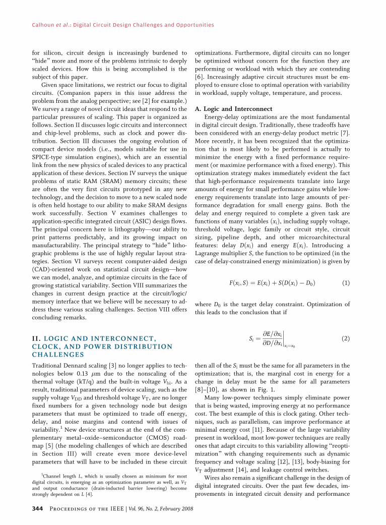
A. Logic and InterconnectEnergy-delay optimizations are the most fundamental
in digital circuit design. Traditionally, these tradeoffs have
been considered with an energy-delay product metric [7].
More recently, it has been recognized that the optimiza-
tion that is most likely to be performed is actually to
minimize the energy with a fixed performance require-
ment (or maximize performance with a fixed energy). This
optimization strategy makes immediately evident the fact
that high-performance requirements translate into largeamounts of energy for small performance gains while low-
energy requirements translate into large amounts of per-
formance degradation for small energy gains. Both the
delay and energy required to complete a given task are
functions of many variables ðxiÞ, including supply voltage,threshold voltage, logic family or circuit style, circuit
sizing, pipeline depth, and other microarchitectural
features: delay DðxiÞ and energy EðxiÞ. Introducing aLagrange multiplier S, the function to be optimized (in the
case of delay-constrained energy minimization) is given by
Fðxi; SÞ ¼ EðxiÞ þ S DðxiÞ � D0ð Þ (1)
where D0 is the target delay constraint. Optimization of
this leads to the conclusion that if
Si ¼@E=@xi@D=@xi
����xi¼x0
(2)
then all of the Si must be the same for all parameters in the
optimization; that is, the marginal cost in energy for a
change in delay must be the same for all parameters
[8]–[10], as shown in Fig. 1.
Many low-power techniques simply eliminate power
that is being wasted, improving energy at no performance
cost. The best example of this is clock gating. Other tech-
niques, such as parallelism, can improve performance atminimal energy cost [11]. Because of the large variability
present in workload, most low-power techniques are really
ones that adapt circuits to this variability allowing Breopti-mization[ with changing requirements such as dynamic
frequency and voltage scaling [12], [13], body-biasing for
VT adjustment [14], and leakage control switches.
Wires also remain a significant challenge in the design of
digital integrated circuits. Over the past few decades, im-provements in integrated circuit density and performance
1Channel length L, which is usually chosen as minimum for mostdigital circuits, is emerging as an optimization parameter as well, as VTand output conductance (drain-inducted barrier lowering) becomestrongly dependent on L [4].
Calhoun et al.: Digital Circuit Design Challenges and Opportunities
344 Proceedings of the IEEE | Vol. 96, No. 2, February 2008
have been achieved by scaling down transistors. Latency
(rather than pipelined throughput) of on-chip wires is
important for many applications such as buses between
cache memories and processors [15]. Although the latenciesof local interconnects scale accordingly, the delay per unit
length of on-chip wires, as determined by a diffusive RC-limited response and as measured relative to gate delays,
approximately doubles every technology generation [16],
[17] as wire resistances per unit length increase and gate
delays decrease with scaling. Furthermore, these wire
delays ðDÞ grow quadratically with wire length D /RwireCwireL
2. Wire bandwidths, which are inversely propor-tional to D, also degrade.
Buffers (or repeaters) are traditionally added to make the
interconnect latency linear with wire length, with simple
relationship guiding an optimal number of repeaters (and
their sizing) to minimize interconnect delay [16]. Wide wires
can be used to improve overall latency, requiring fewer
numbers of repeaters of larger area (to drive the larger wire
capacitance) to achieve a delay optimal solution. Overallenergy-per-bit and routing density, however, degrade with
wire widening [16].
Interconnect latency, bandwidth density (bits per
second per unit routing width), and energy-per-bit for
on-chip wires can be improved with more intelligent cir-
cuits, moving beyond the use of a full-rail RC-limited
interconnect buffered by CMOS inverters for on-chip
communications. On-chip RC links that run low-swing canprovide an order of magnitude improvement in energy-per-
bit, but generally do so at the cost of degraded latency [18],
[19]. Other circuit approaches take advantage of transmis-
sion line effects to simultaneously improve latency and
energy-per-bit, including pulsed current-model signaling
[20] and the use of distributed loss compensation [21].
The clock and power networks in digital integrated
circuits present important additional challenges and areconsidered in detail in the following two sections.
B. Clock DistributionClock distribution remains an important challenge in the
design of large-scale digital chips, a challenge that has only
grown with technology scaling. Most modern clock distribu-
tions are Bsingle wire,[ meaning that only a single clock
phase is distributed globally although multiple clock phases
are often created locally with clock Bshaper,[ clock
Bchopper,[ or clock buffer circuits. The challenge of clock
distribution is to distribute the clock simultaneously every-where (no skew) and periodically everywhere (no jitter)
using minimal power and wiring resources and being as
impervious as possible to process variations and supply noise.
The typical Bgain[ of a clock distribution network, as
measured by the ratio of the clock load capacitance to the
capacitance driven from the phase-locked-loop reference, is
more than 105.
Clock distributions are typically designed as trees ortree-driven grids. Tree distributions consume the mini-
mum wiring resources and provide the minimum wiring
capacitance (and consequently represent the low-power
solution). They unfortunately suffer from the most
sensitivity to spatial variation (in either load capacitance
or buffer strength). Active deskewing circuits [22] are one
way to address this limitation for trees but add to clock
latency. The addition of a grid to the tree [23] also helps toamortize this variation at the expense of additional wiring
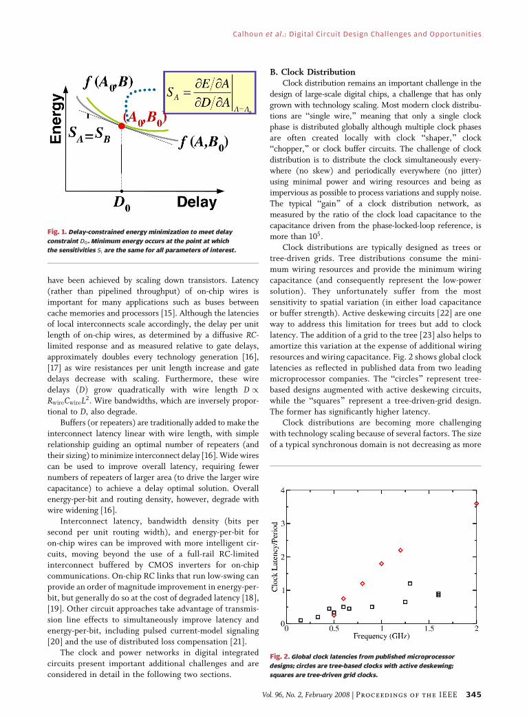
resources and wiring capacitance. Fig. 2 shows global clock
latencies as reflected in published data from two leading
microprocessor companies. The Bcircles[ represent tree-
based designs augmented with active deskewing circuits,
while the Bsquares[ represent a tree-driven-grid design.
The former has significantly higher latency.
Clock distributions are becoming more challengingwith technology scaling because of several factors. The size
of a typical synchronous domain is not decreasing as more
Fig. 2. Global clock latencies from published microprocessor
designs; circles are tree-based clocks with active deskewing;
squares are tree-driven grid clocks.
Fig. 1. Delay-constrained energy minimization to meet delay
constraint D0. Minimum energy occurs at the point at which
the sensitivities Si are the same for all parameters of interest.
Calhoun et al.: Digital Circuit Design Challenges and Opportunities
Vol. 96, No. 2, February 2008 | Proceedings of the IEEE 345

function is integrated onto chips with the availability ofadditional transistors. The relative nonscaling of wire
delay and the increasing amount of capacitance per unit
area exacerbate clock latency and increase the required
gain of the clock network. Variability in process, temper-
ature, and voltage, both temporal and spatial, make skew
and jitter management increasingly difficult. Growing
clock latency (as reflected in Fig. 2) presents challenges in
the presence of variability. For example, for a four-cycleclock latency, a 10% delay variation will result in skew and
jitter that is 40% of the clock cycle time (assuming a tree
distribution, all silicon delay, and no common paths
between clock and data). Jitter from power supply noise
can also vary across the chip and change every cycle.
These challenges have led to a search for circuit alter-
natives for clock distribution networks. Resonant clock dis-
tributions have been proposed as an alternative clocktechnology and have shown promise in reducing clock
timing uncertainty and power dissipation [24]. Standing-
wave clock distributions have been implemented at both the
board level [25] and chip level [26]. These designs achieve
low-skew and low-jitter clocks and can save power due to the
resonance between the clock capacitance and the clock wire
inductance. Standing-wave clock distributions must, how-
ever, contend with nonuniform clock amplitude, which mayresult in skew or make local clock buffering more complex.
Traveling-wave clock distributions [27] use coupled trans-
mission line rings to generate a low-skew and low-jitter clock
and also benefit from the power advantage of resonance.
Nonuniform phase across the distribution makes integration
with existing local clocking methodologies more difficult,
however.
Resonant-load global clock distribution allows thedistribution of uniform-phase uniform-amplitude clock
waveforms by augmenting traditional tree-driven grids
with a set of spiral inductors, which resonates with the
clock load capacitance [28], [29]. A sizable portion of the
jitter reduction and power savings results from reducing
the strength of the clock buffers driving the resonant load,
exploiting the proclivity of the network to sustain a tone at
the target resonant frequency, resulting in a nearly sinu-soidal clock signal. Sinusoidal clocks are however generally
undesirable because of slower signal transition times,
which exacerbate timing uncertainty at single-ended local
clock buffers in the presence of process, voltage, and tem-
perature variations. Another drawback associated with the
resonant-load global clock distribution is the requirement
for large on-chip decoupling capacitance to serve as a
charge reservoir.These issues are addressed in an improved resonant
clock design based on a differential oscillator (DDO)
global clock network [30], [31]. The differential distribu-
tion is a free-running oscillator injection-locked to an
external reference with symmetric inductors placed be-
tween the two clock phases, eliminating the need to add
large capacitors to the clock. At resonance, the DDO global
clock is uniform in both amplitude and phase across thedistribution. Differential detection at the local clock
buffers reduces skew and jitter due to power-supply noise,
process variations, and other common-mode noise sources,
mitigating the disadvantages of the more sinusoidal clocks
characteristic of resonant distributions.
C. Power Supply Distribution, Regulation,and Measurement
With technology scaling and increasing performance
requirements, the power levels to the chip are increasing
while the supply voltages are decreasing. This leads to a
rapid increase in the supply current requirements. With
increasing current transients and average current levels,
more on-chip decoupling capacitance is required while the
resistance and inductance of the power distribution net-
work (including on-chip wiring, pins, sockets, and con-nectors) must be kept stringently low for supply integrity.
Operating at supply voltages below 1 V, 90-nm (and below)
technologies still demand in excess of 100 W of power in
the largest chips, such as high-performance micropro-
cessors. The demands for no more than 10% power supply
variation require impedances on the power distribution of
less than 1 m�, putting unprecedented demands on the
power distribution.On-chip measurement of the power supply is an
important first step in understanding the nature of power
supply noise. On-chip samplers [32] have been used to
make simple sampling oscilloscopes [33] to measure on-
chip supply noise. Measurements on real microprocessors
have also been demonstrated [34].
Active on-chip regulation, similar to that employed for
on-board voltage regulation modules, as implemented withhigh-bandwidth push–pull linear regulators could help to
reduce on-chip decoupling capacitance requirements.
Other circuit approaches have been considered to reduce
current demands in the power distribution outright. One
such approach [35], [36] achieves implicit on-chip dc–dc
conversion by Bstacking[ logic and recycling charge from
one domain to another. Logic is stacked n-high and
operated at an nVDD supply. By stacking the logic domainsn high, the on-chip current demands on the power and
ground networks are also reduced by a factor of n over the
case of all of the domains running in parallel at VDD. Due
to inevitable charge mismatches between the domains of
the stack, the internal node voltages require regulation,
which can be achieved by the addition of push–pull linear
regulators and decoupling capacitors.
III . DEVICE MODELING CHALLENGES
Device models are the critical interface between the
underlying technology and integrated circuit design. Cou-
pled with circuit simulation tools, they significantly improve
design productivity, providing insight into the relationship
between design choices and circuit performance. In order to
Calhoun et al.: Digital Circuit Design Challenges and Opportunities
346 Proceedings of the IEEE | Vol. 96, No. 2, February 2008
guarantee design quality, device models should be scalable
with latest technology advances, accurate across a wide
range of process and operation conditions, and efficient for
large-scale computation. As CMOS technology scales intothe sub-50-nm regime, these modeling demands are
tremendously challenged, especially by the introduction of
alternative device materials and structures, as well as the
ever-increasing amount of process variations.
The scaling of traditional bulk CMOS structure is
slowing down in recent years as fundamental physical
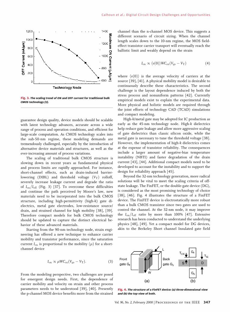
and process limits are rapidly approached. For instance,
short-channel effects, such as drain-induced barrier-lowering (DIBL) and threshold voltage ðVTÞ rolloff,
severely increase leakage current and degrade the ratio
of Ion=Ioff (Fig. 3) [37]. To overcome these difficulties
and continue the path perceived by Moore’s law, new
materials need to be incorporated into the bulk CMOS
structure, including high-permittivity (high-k) gate di-
electrics, metal gate electrodes, low-resistance source/
drain, and strained channel for high mobility [38], [39].Therefore compact models for bulk CMOS technology
should be updated to capture the distinct electrical be-
havior of these advanced materials.
Starting from the 90-nm technology node, strain engi-
neering has offered a new technique to enhance carrier
mobility and transistor performance, since the saturation
current Ion is proportional to the mobility ð�Þ for a short-channel device
Ion / �WCoxðVgs � VTÞ: (3)
From the modeling perspective, two challenges are posed
for emergent design needs. First, the dependence of
carrier mobility and velocity on strain and other process
parameters needs to be understood [39], [40]. Presently
the p-channel MOS device benefits more from the strained
channel than the n-channel MOS device. This suggests adifferent scenario of circuit sizing. When the channel
length scales down to the 10-nm regime, the MOS field-
effect transistor carrier transport will eventually reach the
ballistic limit and weakly depend on the strain
Ion / vð0Þh iWCoxðVgs � VTÞ (4)
where hvð0Þi is the average velocity of carriers at the
source [39], [41]. A physical mobility model is desirable to
continuously describe these characteristics. The second
challenge is the layout dependence induced by both the
stress process and nonuniform patterns [42]. Currently
empirical models exist to explain the experimental data.
More physical and holistic models are required through
the joint efforts of technology CAD (TCAD) simulationsand compact modeling.
High-k/metal gate may be adopted for IC production as
early as the 45-nm technology node. High-k dielectrics
help reduce gate leakage and allow more aggressive scaling
of gate dielectrics than classic silicon oxide, while the
metal gate is necessary to tune the threshold voltage [38].
However, the implementation of high-k dielectrics comes
at the expense of transistor reliability. The consequencesinclude a larger amount of negative-bias temperature
instability (NBTI) and faster degradation of the drain
current [43], [44]. Additional compact models need to be
developed to account for the instability and to support the
design for reliability approach [45].
Beyond the 32-nm technology generation, more radical
solutions will be vital to meet the scaling criteria of off-
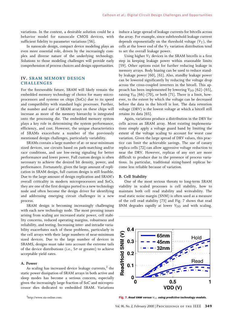
state leakage. The FinFET, or the double-gate device (DG),is considered as the most promising technology of choice
[38], [46]. Fig. 4 illustrates the structure of a FinFET
device. The FinFET device is electrostatically more robust
than a bulk CMOS transistor since two gates are used to
control the channel. At the 32-nm node, it may improve
the Ion=Ioff ratio by more than 100% [47]. Extensive
research has been conducted to understand the underlying
physics [48], [49]. Yet a compact model for DG devices,akin to the Berkeley Short channel Insulated gate field
Fig. 3. The scaling trend of ON and OFF current for traditional bulk
CMOS technology [1].
Fig. 4. The structure of a FinFET device: (a) three-dimensional view
and (b) the top view of both.
Calhoun et al.: Digital Circuit Design Challenges and Opportunities
Vol. 96, No. 2, February 2008 | Proceedings of the IEEE 347

effect transistor Model (BSIM) and Pennsylvania State
University-Philips (PSP) model [50] for the bulk CMOS
transistor, has not been standardized. Alternatively, an
equivalent subcircuit model is proposed in [47], which
models a FinFET device as two silicon-on-insulator (SOI)
transistors with common source and drain. The unique
property of a FinFET device is the electrical coupling be-
tween front and back transistors. Specifically, the thresh-old voltage of the front transistor ðVTfÞ is controlled by theback gate voltage ðVGbÞ, through the partition between the
gate oxide capacitance (Coxb and Coxf) and the silicon body
capacitance ðCSi)
@VTf=@VGb ¼ �ðCSikCoxbÞ=Coxf : (5)
Fig. 5 evaluates the model against the results from TCAD
simulations for a variety of TSi [51]. Such an approach is
compatible with SPICE simulators and enables early stage
design exploration for digital applications.
While technology scaling can be extended with alter-
native materials and structures, CMOS technology willeventually reach the ultimate limits that are defined by
both physics and the fabrication process. One of the most
profound physical effects will result from the vastly in-
creased parameter variations due to manufacturing and
environmental factors [52]. These variations exacerbate
design margins, degrade the yield, and invalidate current
deterministic design methodologies [53]. To maintain de-
sign predictability with those extremely scaled devices,compact models should be extended from the traditional
corner-based approach to a suite of modeling efforts, in-
cluding extraction methods, the decoupling of variation
sources, and highly efficient strategies for the statistical
design paradigm [54].
Process variations usually manifest themselves as
parameter fluctuations in nanoscale transistors, such as
the channel length, threshold voltage, and transistor para-sitics. By characterizing appropriate test structures, these
variations need to be correctly extracted and embedded
into a transistor model file, such that a circuit designer can
perform statistical analysis and optimization to mitigate
performance variability. A rigorous extraction method fur-
ther helps shed light on the mechanism of variations.
The main modeling challenge under variations is to
identify systematic variation components, develop predic-tive models for performance analysis, and incorporate
them into design tools. One example of predictable varia-
tions is the layout-dependent change induced by sub-
wavelength lithography or local stress engineering [54],
[55]. As the semiconductor industry migrates to subwave-
length lithography, there is a growing difference between
the layout viewed in the design stage and that after the
manufacturing process (Fig. 6). The distortion of thelayout shape may lead to more than 20 times increase in
off-state leakage, as demonstrated from the TCAD sim-
ulation at the 65-nm technology node (Fig. 6). This phe-
nomenon demands the construction of compact models
beyond the level of individual devices. The local environ-
ment should be included to account for the interaction
between design, performance, and manufacturability.
Statistical analysis under variations inevitably in-creases the cost of computation. This problem is further
exacerbated as future digital design becomes bigger and
more complex. Therefore, the simplicity of device models is
key to a statistical design flow. Current compact transistor
models consist of a large number of parameters and com-
plicated equations to capture many physical mechanisms
for a short-channel device, but significantly slowing down
the simulation speed. At the other extreme end, lookuptable based approaches are much more efficient; however,
their empirical nature limits the scalability to process
Fig. 5. The coupling between VTf and VGb in a FinFET device.
Fig. 6. Subwavelength lithography causes a nonrectangular gate
shape and the significant increase in leakage.
Calhoun et al.: Digital Circuit Design Challenges and Opportunities
348 Proceedings of the IEEE | Vol. 96, No. 2, February 2008
variations. In the context, a desirable solution could be abehavior model for nanoscale CMOS devices, with
sufficient fidelity to parameter variations [56].
In nanoscale design, compact device modeling plays an
even more essential role, driven by the increasingly com-
plex and diverse nature of the underlying technology.
Solutions to those modeling challenges will provide early
comprehension of process choices and design opportunities.
IV. SRAM MEMORY DESIGNCHALLENGES
For the foreseeable future, SRAM will likely remain the
embedded memory technology of choice for many micro-
processors and systems on chips (SoCs) due to its speed
and compatibility with standard logic processes. Further,
the number and size of SRAM arrays on these chips willincrease as more of the memory hierarchy is integrated
onto the processing die. The embedded memory system
plays a key role in determining the system performance,
efficiency, and cost. However, the unique characteristics
of SRAMs exacerbate a number of the previously
mentioned design challenges, particularly variability.
SRAMs contain a large number of at- or near-minimum
sized devices, use circuits based on path-matching and/orrace conditions, and use low-swing signaling for better
performance and lower power. Full custom design is often
necessary to achieve the desired bit density, power, and
performance. Fortunately, given the large amount of repli-
cation in SRAM design, full custom design is still feasible.
Due to the large amount of design replication and SRAM’s
overall criticality in modern microprocessors and SoCs,
they are one of the first designs ported to a new technologynode and often become the design driver for identifying
and addressing emerging circuit challenges in a new
process.
SRAM design is becoming increasingly challenging
with each new technology node. The most pressing issues
arising from scaling are increased static power, cell stabi-
lity concerns, reduced operating margins, robustness and
reliability, and testing. Increasing inter- and intradie varia-bility exacerbates each of these problems, particularly in
the cell arrays with their large numbers of near-minimum
sized devices. Due to the large number of devices in
SRAMS, designs must take into account the extreme tails
of the device distributions (i.e., 5� or greater) to achieve
acceptable yield rates.
A. PowerAs scaling has increased device leakage currents,2 the
static power dissipation of SRAM arrays in both active and
sleep modes has become a serious concern, especially
given the increasingly large fraction of SoC and micropro-
cessor dies dedicated to embedded SRAM. Variations
induce a large spread of leakage currents for bitcells acrossthe array. For example, since subthreshold leakage current
depends exponentially on the threshold voltage ðVTÞ, thecells at the lower end of the VT variation distribution tend
to set the overall leakage power.
Using higher VT devices in the SRAM bitcells is a first
step in keeping leakage power within reasonable limits
[59]. Other options exist for further reducing leakage in
memory arrays. Body biasing can be used to reduce stand-by leakage power [60], [61]. Also, standby leakage power
can be lowered significantly by reducing the voltage drop
across the cross-coupled inverters in the bitcell. This ap-
proach has been implemented by lowering VDD [62]–[65],
raising VSS [66]–[70], or both [71]. There is a limit, how-
ever, to the extent by which the voltage can be decreased
before the data in the bitcell is lost. The data retention
voltage (DRV) is the lowest voltage at which a bitcell stillretains its data [65].
Again, variations produce a distribution in the DRV for
cells across an SRAM array. Most existing implementa-
tions simply apply a voltage guard band by limiting the
extent of the voltage scaling to account for worst case
variation. Given the large spread of DRV values, this prac-
tice can limit the achievable savings. The use of canary
replica cells [72] can allow aggressive voltage reduction tonear the DRV. However, replicas of any sort are more
difficult to produce due to the presence of process varia-
tions. In particular, traditional sizing-based replicas be-
come less reliable because of variation.
B. Cell StabilityOne of the most serious threats to long-term SRAM
viability in scaled processes is cell stability, how tomaintain both cell read stability and writeability. The
read static noise margin (SNM) is often used as a measure
of the cell read stability [73] and Fig. 7 shows that read
SNM degrades rapidly at lower VDD and with scaling.
2http://www.sia-online.com. Fig. 7. Read SNM versus VDD using predictive technology models.
Calhoun et al.: Digital Circuit Design Challenges and Opportunities
Vol. 96, No. 2, February 2008 | Proceedings of the IEEE 349
Furthermore, the larger variation inherent in advancedtechnologies creates a greater spread in the SNM distr-
ibution. Read SNM rapidly becomes a serious limiter of
voltage and technology scaling [74], [75].
Write margin degrades in a similar fashion. Exacerbat-
ed by large process variations, the write drivers and access
transistors of cells with insufficient write margin cannot
overpower the load inside the cell, preventing successful
write operation. This effect gets worse at low voltage, andit can actually be the primary limitation to voltage scaling
[75], [76].
In the short term, there are a number of techniques to
extend the viability of the traditional 6T SRAM cell to lower
supply voltages and newer technologies. Almost all cutting
edge SRAMs use a variety of voltage knobs to compensate
for variations. For example, lower bitline precharge voltage
[76], [78], boosted cell voltage [79]–[81], and write afterread [78] improve or bypass read SNM. For write accesses,
boosted wordline voltage [75], [81] or collapsed cell voltage
[75], [76], [80], [81] improve the write margin. An ad-
ditional complicating factor in cell design is the printability
of subdesign rule Bpushed[ cell layouts, which further
constrains viable cell sizings and topologies (see Section V).
However, in the long term, whether the 6T cell is the
optimal cell topology choice in nanoscale processes is stillan open question. Other options, such as using alternative
bitcells [77] or dual-port bitcells with read buffers [75],
[81], can eliminate the read SNM problem. There are a
number of attractive alternate cell topologies that, while
they do require more area and/or devices per cell, may
achieve higher overall bit density because they require less
peripheral circuitry. Using alternate or emerging technol-
ogies offers some promising solutions as well. For example,process variations are less severe in SOI than in bulk
CMOS [59], and FinFET-based SRAM cells can offer
improved characteristics [83].
C. Operating MarginsIn addition to the stability of a single cell decreasing,
the operating margins of the memory as a whole are de-
creasing due to scaling effects on the cell arrays andperipheral circuits. Variability in the cells decreases the
minimum expected Ion. Leakage and variability increase
the bitline leakage of the unselected cells, further reducing
the bitline differential voltage. Designers have developed
ways to reduce the Boff[ cell leakage onto the bitlines
which include using long L or high-VT devices, read bit-
lines precharged to less than VDD, leakage cancelling bit-
cells, and active leakage compensation [82]. Variability inthe peripheral circuits also decreases the operating margin
by affecting the sense amplifiers, control signal generation,
and decoders.
Variability is causing sense amplifiers to have large
input-referred offsets. The sense amplifier offset can be
reduced in a number of ways, including using larger de-
vices, shaping the sense enable signal, or active offset
compensations [88], [89]. Alternately, large swing (e.g.,half or full VDD) bitlines can be used, but this comes at the
cost of power and performance.
On a read, clocked sense amplifiers can be fired either
from a clock edge or using a replica timing circuit. The
replica timing circuit mimics the delay of the actual bitline
and tracks that delay over process and environmental
variations [90], which is why it is the preferred method of
sense enable generation for high-performance SRAMs.However, device variations also affect the replica circuit,
further decreasing the read margin. The replica circuit can
be made robust to variations by simply increasing the
number of replica driver cells (and proportionally
increasing the replica load), but this requires a large
number of replica driver cells to achieve average-case
matching. Future replica circuits will require variability
tolerant driver cells or a way to configure the driver cellssuch that they achieve average-case performance.
Decoder design will also require a rethink in nanoscale
processes. Previous high-performance designs used pulse-
mode self-resetting logic for high-speed and low-power
[90]. However, these logic styles often relied on race con-
ditions and had numerous timing constraints. With in-
creasing variability, these logic styles become increasingly
difficult to design in a robust and manufacturable way.Also, high-performance decoders have used low-VT devices
for better performance, but leakage in these devices will
contribute significantly to leakage power.
To combat these trends, future designs will likely use
higher degrees of bitline segmentation to decrease the
number of cells on a bitline, larger swing signaling to
account for the decreased bitline differential voltages, and
generally more conservative circuit design given the ero-sion of previously held assumptions about cell, device, and
path matching. Bit density and performance will likely not
scale as quickly as in past generations, given the more
conservative approach to design.
D. Robustness and ReliabilityWith scaling, hard and soft errors in SRAM will
increase in frequency and scope, so that a single errorevent is more likely to cause multiple bit failures within a
single word and across multiple words [91]. There are a
number of causes of soft errors including energetic particle
strikes, signal or power-supply noise coupling, and erratic
device behavior [84]–[86], [93]. In today’s technologies,
the vast majority of soft error events will result in only a
single cell’s being disturbed, but as we scale into the nano-
meter regime, single event multibit errors will becomemore and more likely [91]. While the failures-in-time (FIT)
rate of an individual SRAM cell will remain approximately
constant across process technology due to the propor-
tionate shrinking of the cell Qcrit and collection area, the
overall chip FIT rate will increase due to the increasing
number of SRAM cells on a die [91]. Additionally, the
number of SRAM cells that fall under the footprint of a
Calhoun et al.: Digital Circuit Design Challenges and Opportunities
350 Proceedings of the IEEE | Vol. 96, No. 2, February 2008
single energetic particle strike will increase, since theparticle strike footprint does not scale, and thus increase
the likelihood of multibit upsets.
Hard errors are the result of a number of phenomena
including electromigration, device wearout/aging (e.g.,
oxide breakdown, NBTI), and highly energetic particle
strikes. Hard errors can result in large-scale data loss, such
as an entire data row or column, pairs of rows or columns,
or even an entire subarray [94], [95]. In deeply scaledprocesses, the incidence of hard error at manufacture time
and in the field is expected to rise dramatically [95], [96].
This large-scale information loss and high rate of hard
errors will likely overwhelm conventional memory protec-
tion techniques and threatens both the yield rate and run-
time reliability of chips with large embedded memories.
Finally, inter- and intradie variability not only in-
creases the percentage of memory cells and peripherallogic blocks that fail altogether (e.g., from insufficient read
static noise margin in a 6T SRAM cell) but also increases
the number of cells and peripheral logic blocks that are
marginally functional and thus more susceptible to hard
and soft error phenomena.
To combat hard and soft errors, designers currently
employ a number of techniques, including error-correcting
codes (ECCs), bit-interleaving, redundancy, and device-level countermeasures. Single error correct, double error
detect (SECDED) ECC is widely used in modern memories
for soft error protection. SECDED ECC can also be used
for yield enhancement by letting the ECC code correct
single-bit, manufacture-time, hard errors, but this sacri-
fices soft error immunity for the data words that have a
preexisting hard error from manufacturing [97]–[99]. Bit-
interleaving (also known as column multiplexing) is oftenemployed for higher performance and easier layout, but in
combination with ECC, it allows the correction of small-
scale multibit errors that have a footprint less than or equal
to the degree of interleaving. Unfortunately, the degree of
bit-interleaving cannot be increased much beyond four
before incurring significant performance and power
penalties [100]. To map out manufacture-time hard errors
and thus improve yield, modern SRAM designs use re-dundant rows, columns, and subarrays. Combined with
built-in self-test (BIST) or built-in self-repair (BISR)
mechanisms, the memories can detect and repair hard
errors during both manufacturing test and in-the-field
operation [101]–[103].
In addition to microarchitecture mechanisms based on
error detection and rollback [105], and logic and circuit-
level mechanisms that strive to harden sensitive bit-levelstorage elements [106], [107], there are a number of
process-level techniques to reduce soft errors such as
SOI processes, explicit capacitors to increase Qcrit, and
specialized hardened processes primarily used for space
applications. These techniques often require expensive
additional mask layers and processing steps to implement
the explicit capacitors. While effective for the error rates
and types seen today, these conventional techniques willnot scale to cover the high incidence of error and multibit
error events that will occur in nanoscale technologies.
Thus, an efficient multibit error protection scheme is
necessary to ensure high efficiency, reliable operation, and
high yield for future memory-intensive ICs.
Finally, memory test and design for testability will
likely become primary design considerations, as the num-
ber and size of deeply embedded SRAM arrays in SoCs andmicroprocessors dies increase. BIST and BISR will become
a necessity for these deeply embedded memory arrays. By
itself, memory test is a large and critical field [108], [109],
coverage of which lies outside of the scope of this design-
focused paper. Yet the role of BIST/BISR circuitry will
expand beyond testing for faulty/marginal circuits at man-
ufacture time to include characterization of the die (or
portion of the die) to enable postmanufacturing self-tuningof the entire die or individual components on the die.
Researchers have already proposed using on-die leakage
characterization circuits to guide tuning of the back bias
voltage for process centering to combat interdie process
variations [87]. As inter- and intradie variability becomes
more pronounced, designers will likely need to incor-
porate more knobs for postmanufacturing tuning, and
BIST/BISR circuits will play a critical role in the tuningcontrol loop.
E. Design Methodology, Tools, and OptimizationGiven the large number of design and topology
choices, as well as the necessary multidimensional opti-
mization problem, SRAM design and optimization by
hand is becoming increasingly infeasible. To find the
optimal design, SRAM designers will require optimiza-tion and design tools that allow for fast exploration of the
design space. These tools will need to operate at a higher
level than today’s transistor-level circuit optimizers (e.g.,
IBM’s EinsTuner, Stanford’s Circuit Optimization Proj-
ect, CMU’s ROAD, Cadence’s NeoCircuit) and offer more
degrees of freedom than today’s memory compilers. This
new class of memory design tools must offer memory
synthesis capability similar to today’s logic synthesis toolchain. Taking in design and process constraints along
with a precharacterized set of memory circuit topologies,
the tool would produce a set of memory designs along the
Pareto-optimal surface. One of the primary challenges in
developing this type of tool is performing design opti-
mization across multiple levels of the design stack, from
process technology to microarchitecture. Capturing a
sufficiently wide range of circuit topologies to coverwidely separated points in the SRAM design space (e.g.,
low-power designs versus high-performance designs) and
different process technology choices will also pose a
significant challenge.
Because robustness and yield will be key optimization
goals, such a tool will also require extensive simulations
under process variations. Efficient Monte Carlo simulation
Calhoun et al.: Digital Circuit Design Challenges and Opportunities
Vol. 96, No. 2, February 2008 | Proceedings of the IEEE 351
tools targeted at rapid exploration and sampling from thestatistically rare tails of the variation distributions will be
critical. Research efforts in this area include ideas from
Monte Carlo mixture importance sampling [104] and the
recently introduced statistical blockade technique [133],
which we shall describe further in Section VI-A.
Due to the increasingly difficult design environment in
scaled technologies, SRAM designers must take advantage
of opportunities at all levels of the design stack, especiallyoften overlooked solutions at microarchitecture and archi-
tecture levels. Codesign will have to occur across process
technology, circuits, and microarchitecture to meet future
power, area, and performance targets.
V. CHALLENGES TO DIGITALDESIGN FLOWS
A. Lithography, Manufacturability, and RegularityIn the past, complying with design rules was sufficient
to ensure acceptable yields for circuits designed in a spe-
cific technology. However, for sub-90-nm technology de-
signs, this approach tends to create physical geometrypatterns that cannot be reliably printed for a given litho-
graphy setup, thus leading to hot spots and systematic yield
failures.
Correspondingly, the economics of chip design have
been changing as these technology challenges become more
prominent with each process generation. For instance, even
though the design complexity has been increasing, the time-
to-market (or time-to-mission for military applications) hasbeen steadily shrinking as well. Missing the market window
can be catastrophic, as the proper demand for the product
might exist for only a short period of time. This fast pace
has resulted in concurrent process and product develop-
ment, as companies can no longer afford to complete pro-
cess development before starting out with product design.
The practice of debugging designs in silicon, therefore, be-
comes economically infeasible, and there is increasingpressure for the silicon to work correctly the first time.
Present ASIC design methodologies break down in light
of these new economic and technology realities, and new
design methodologies are required for which the physical
implementation of the design is more predictable. For
several generations, migration to the next process node has
relied primarily upon optical lithography to shrink feature
sizes. It is apparent, however, that the challenges intro-duced in the sub-100-nm regime will make such scaling
intractable without a corresponding change in the design
methodology. An especially promising solution strategy is
one based on so-called regular design fabrics; we discuss theconcept of regularity and its consequences in this section.
B. Lithographic Challenges to Design MethodologyMoore’s law scaling [1] relies on the ability to shrink
feature sizes of the IC by approximately 70% in each
process generation. As a direct result of the aggressivescaling, the industry is now operating in the nanometer
regime. However, as feature sizes continue to scale, the
industry is beginning to experience a number of difficul-
ties, thus calling into question the pace of scaling that has
been the de facto standard.For the industry to continue to progress with CMOS
scaling and ultimately beyond, a paradigm shift is required
whereby circuits are constructed from a small set of litho-graphy friendly patterns that have previously been exten-
sively characterized and ensured to print reliably. Two of
the more prominent approaches are based on the use
restricted design rules (RDRs) [110] and/or regular designfabrics [111], [112]. There are, of course, several other ap-proaches that are motivated by the same problems [113]–
[116]; namely, the functional and parametric yield failures
associated with subwavelength lithography for nanoscalepattern features.
In the past, lithographers have relied on aggressively
scaling the wavelength of light to enable classical CMOS
scaling. In the face of recent challenges with developing
cost-effective lithography systems that can operate at
shorter wavelength of light, the industry has explored
alternative techniques to aggressively shrink feature sizes
while using the same light source. Most of these tech-niques rely on the use of strong resolution enhancement
techniques (RETs), such as off-axis illumination and alter-
nating aperture phase-shift masks (altPSM) [117], [118].
Although the use of RETs can improve the image quality of
some patterns in the design, they tend to compromise the
image quality of other patterns present in the layout. Such
non-RET compliant patterns need to be identified and
eliminated from the design in order to create RET-compliant design. The implementation of such an RET-
compliant design is a very difficult task in general [119].
Nanoscale lithography generates a rather daunting set
of problems that we must address; we enumerate the
essential set of problems in the rest of this section.
1) Failure of Layout Design Rules: Design rules not only
act as a means to integrate IC design and manufacturingbut also serve to isolate both the design and manufacturing
communities from the challenges faced by the other. The
design rules attempt to define the limits for a given process
in terms of overly simplified design constraints. Tradi-
tionally, a simple set of design rules was sufficient to
ensure a Bwhat you see is what you get[ (WYSIWYG)
paradigm that would still produce sufficient product yield.
But as feature sizes continued to shrink, a simple set ofdesign rules is incapable of documenting all the complex
physical, chemical, and mechanical phenomenon that
occur in a manufacturing process. In order to extend the
WYSIWYG design paradigm, process engineers have intro-
duced additional design rules to account for failures that
occur due to lithography, chemically mechanically po-
lished, etch-loading, stresses in dielectrics, and other
Calhoun et al.: Digital Circuit Design Challenges and Opportunities
352 Proceedings of the IEEE | Vol. 96, No. 2, February 2008

complex physical, chemical, and mechanical interactions. Inaddition, the need for RET-compliant lithography friendly
designs in more advanced process technologies has further
increased the raw number and the complexity of these rules
[117]. In addition, the new expanded set of BDFM[ design
rules often leads to rules that are contradictory and con-
flicting to existing design rules and goals. Consequently,
designs that comply with this expanded set of design rules
tend to be less efficient in terms of area, timing, and power.Besides, even after complying with the expanded set of
design rules, designs in the sub-100-nm regime still do not
provide sufficient yield during manufacturing and require
multiple design respins prior to reaching market.
2) Geometry Pattern Explosion: The problem with design
respins is correlated with the large number of patterns
that must be precharacterized and validated prior to finalproduct implementation. Most importantly, the set of
patterns is design-dependent; therefore, the task of char-
acterizing a manufacturing process becomes impossible,
as one has to account for the all possible patterns in a
design. As a result, a process is only characterized and
qualified for a small set of test patterns, and it is not
uncommon to observe some uncharacterized patterns in
the design that are difficult to manufacture, hence moreprone to failures. In several cases where critical failures
have occurred frequently, both design respins and process
retargeting were warranted in order to ramp up yield of
the product. Such unwanted increase in nonrecurring
engineering costs has also been an area of concern for the
industry, where designers have become reluctant to scale
designs to more advance process technologies.
3) Drawback of Existing Design Flows: A conventional
ASIC design flow begins with a high-level specification of
the intended behavior of the circuit. This is often accom-
plished through the use of a register transfer level (RTL)
description of the circuit. An RTL netlist describes the
functionality of the circuit in the form of transfer functions
that are linked by registers. A logic synthesis step converts
the RTL into a gate-level netlist. The synthesis step in-cludes a series of logic optimization steps to find a solution
that meets the required design constraints, such as area,
timing, and power. As such, the logic synthesis relies on
the existence of a predefined library of logic gates to
translate the RTL into a gate-level netlist while making the
appropriate tradeoffs between design constraints. These
logic gates are commonly referred to as standard cells, with
the collection of them being referred to as a standard celllibrary. A standard cell library for a modern technology
node can easily consist of several hundred, or even thou-
sands, of these standard cells. In the final step of a con-
ventional ASIC design flow, the standard cells are arranged
next to each other and routed according to the connections
defined in the gate level netlist, in a manner that meets
both the timing and area constraints of the design.
In the past, it was sufficient to ensure manufacturabilityof each individual standard cell to guarantee manufactur-
ability of the entire chip. However, the complex optical
interactions in sub-100-nm lithography make it difficult to
predict the manufacturability and behavior of each standard
cell under the influence of all the possible neighborhoods it
might experience in an IC design. It is not surprising that
the borders of these standard cells are breeding grounds for
hotspots, as shown in Fig. 8. The simulation shown in thisfigure consists of two standard cell flip-flops. The flip-flop
on the left has no cells on its left, whereas the flip-flop on
the right has a flip-flop to its left. It can be observed that the
neighborhood of the design strongly influences the presence
of hot spots. Hence, the only methodology to ensure manu-
facturability of the entire library is to verify printability of
each standard cell in all of the possible neighborhoods
taking into account all possible cell abutments. For astandard cell library consisting of 1000 standard cells, there
are �2 million possible configurations in which one can
arrange a pair of standard cells. Moreover, as the feature
sizes continue to shrink without reducing the wavelength of
light being used, the complex optical interactions can ex-
tend past the nearest cell in the design. As such, the number
of possible configurations makes the characterization of an
entire standard cell library an intractable task.
C. The Need for Design RegularityLimiting the number of layout patterns required to
implement a design in a particular technology can greatly
simplify the required RETs. Specifically, construction of
the design out of a set of geometric patterns that are
guaranteed to manufacture and can be well controlled to
reduce variability will address the failures associated withmodeling complex semiconductor processes by a set of
simplistic design rules. Moreover, design methodologies
that do not rely on the existence of large standard cell
libraries can further reduce the number of patterns present
in the ASIC design. Hence, design regularity must occur at
both the pattern level and the gate/logic level. We address
the former in terms of microregularity, and the latter with
constraints on macroregularity.
1) Restrictive Design Rules: The use of RDRs has been
proposed in the literature [110], [117]. These RDRs are
used during physical design and account for the design
intent. RDRs are designed to be RET generic and also serve
to reduce optical proximity correction (OPC) complexity.
The essence of RDRs is that they overcome challenges in
implementing RETs by a paradigm shift in tools, flow, andmethodology instead of introducing small changes in con-
ventional design rules [110]. The key concepts introduced
by RDRs are:
• use of smaller range of line widths for critical
patterns;
• critical features such as gates aremade unidirectional
to decrease across-chip linewidth variation (ACLV);
Calhoun et al.: Digital Circuit Design Challenges and Opportunities
Vol. 96, No. 2, February 2008 | Proceedings of the IEEE 353

• critical features are placed on grid (integer multi-
ples of critical pitch);
• limit possible combinations of proximities for critical
features (e.g., for critical gates select critical pitch).
This RDR microregularity improves pattern uniformity
within a Bmacro[ cell. Orientation and critical pitches can
be varied from block to block as long as the pitch lies
within a set of well characterized pitches. The reduction ofACLV is demonstrated in [110]. Three hundred percent
reductions in ACLV are reported using RDRs. Reference
[110] also shows that design rule checking, OPC, and
altPSM generation are significantly simplified by using
RDRs. Importantly, RDRs are effective for designs that are
restricted and optimized for a particular process. To make
designs portable across foundries, as is required for low-
volume ASICs and fabless design houses, a more stringentset of design rules are required.
2) Gridded Layouts: A repeating set of alternating dark
(lines) and clear (spaces), known as a grating, is the
simplest and most lithography-friendly patterning. The use
of gridded layouts would assist in the optimization of
manufacturability and decrease cost, but at the expense of
increased area. The cost and area tradeoff can be mini-mized by selecting an optimal pitch, hence determining a
grid pitch is critical [118]. To reduce the area penalty, the
use of gridded layouts is sometimes suggested only for
polysilicon (gates) and contact levels in the direction
parallel to the lengths of the transistors [118]. Using the
same horizontal pitch for contact and gate can decrease the
manufacturing cost and enable the use of template trim
lithography. Detailed characterization of the process atthis critical pitch can improve circuit performance by
reducing variability.
3) Macroregularity: Macroregularity, which is the limiting
of the number of patterns by limiting the number of unique
Bmacro[ pattern groupings, can provide considerable benefitfor overcoming the penalties associated with microregular
gridding alone. For example, field-programmable gate arrays
(FPGAs) and memory designs have relied primarily on their
macroregularity (e.g. bit-cell repeatability and known neigh-
borhood of other bit-cells) to address the manufacturability
challenges posed by new technology nodes. Due to the
limited number of unique shapes present, one can afford toperform RETs, simulation-based modeling, and silicon
verification for the small structures as they will ultimately
appear, surrounded by the regular geometry neighborhood of
other cells. It is for this reason that memories and FPGAs are
often the first products to utilize a new manufacturing
process.
Recently, new methodologies have been proposed for
design of regular logic structures that literally combinethe benefits of programmable devices (FPGAs) and
application-specific customized designs [115], [116],
[120]–[122]. These approaches are based on an underly-
ing regular fabric for the logic that is constructed from
configurable logic blocks, much like FPGAs and memories
that can be fine-tuned for manufacturability and perfor-
mance based on the layers that are shared for multiple
designs and applications. Recent work on via-configurableregular fabrics in particular has shown that fabrics built
from a fully programmable universal block, capable of
being configured to implement many different functions,
can simplify the synthesis process while providing per-
formance comparable to that of ASIC implementations
[120]–[122]. The simplified synthesis process, however,
can sometimes correspond to poor silicon utilization, and
hence larger designs and possibly increased yield loss dueto random defects. Moreover, these approaches cannot
attain the power and performance that can be achieved by
full customization, and they will waste considerable area
due to underutilized logic and memory, which are defined
by fixed footprints across multiple applications.
Fig. 8. Lithography simulation showing hotspots as a function of pattern neighborhood.
Calhoun et al.: Digital Circuit Design Challenges and Opportunities
354 Proceedings of the IEEE | Vol. 96, No. 2, February 2008
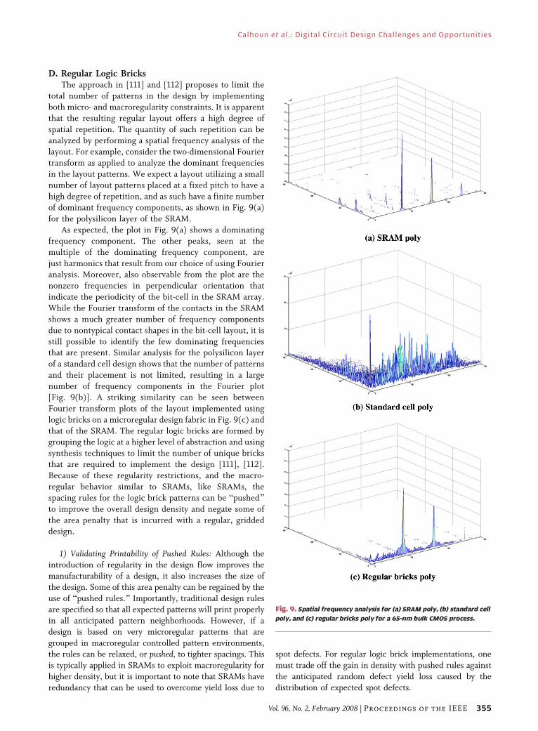
D. Regular Logic BricksThe approach in [111] and [112] proposes to limit the
total number of patterns in the design by implementing
both micro- and macroregularity constraints. It is apparent
that the resulting regular layout offers a high degree of
spatial repetition. The quantity of such repetition can be
analyzed by performing a spatial frequency analysis of the
layout. For example, consider the two-dimensional Fourier
transform as applied to analyze the dominant frequenciesin the layout patterns. We expect a layout utilizing a small
number of layout patterns placed at a fixed pitch to have a
high degree of repetition, and as such have a finite number
of dominant frequency components, as shown in Fig. 9(a)
for the polysilicon layer of the SRAM.
As expected, the plot in Fig. 9(a) shows a dominating
frequency component. The other peaks, seen at the
multiple of the dominating frequency component, arejust harmonics that result from our choice of using Fourier
analysis. Moreover, also observable from the plot are the
nonzero frequencies in perpendicular orientation that
indicate the periodicity of the bit-cell in the SRAM array.
While the Fourier transform of the contacts in the SRAM
shows a much greater number of frequency components
due to nontypical contact shapes in the bit-cell layout, it is
still possible to identify the few dominating frequenciesthat are present. Similar analysis for the polysilicon layer
of a standard cell design shows that the number of patterns
and their placement is not limited, resulting in a large
number of frequency components in the Fourier plot
[Fig. 9(b)]. A striking similarity can be seen between
Fourier transform plots of the layout implemented using
logic bricks on a microregular design fabric in Fig. 9(c) and
that of the SRAM. The regular logic bricks are formed bygrouping the logic at a higher level of abstraction and using
synthesis techniques to limit the number of unique bricks
that are required to implement the design [111], [112].
Because of these regularity restrictions, and the macro-
regular behavior similar to SRAMs, like SRAMs, the
spacing rules for the logic brick patterns can be Bpushed[to improve the overall design density and negate some of
the area penalty that is incurred with a regular, griddeddesign.
1) Validating Printability of Pushed Rules: Although the
introduction of regularity in the design flow improves the
manufacturability of a design, it also increases the size of
the design. Some of this area penalty can be regained by the
use of Bpushed rules.[ Importantly, traditional design rules
are specified so that all expected patterns will print properlyin all anticipated pattern neighborhoods. However, if a
design is based on very microregular patterns that are
grouped in macroregular controlled pattern environments,
the rules can be relaxed, or pushed, to tighter spacings. Thisis typically applied in SRAMs to exploit macroregularity for
higher density, but it is important to note that SRAMs have
redundancy that can be used to overcome yield loss due to
spot defects. For regular logic brick implementations, one
must trade off the gain in density with pushed rules against
the anticipated random defect yield loss caused by the
distribution of expected spot defects.
Fig. 9. Spatial frequency analysis for (a) SRAM poly, (b) standard cell
poly, and (c) regular bricks poly for a 65-nm bulk CMOS process.
Calhoun et al.: Digital Circuit Design Challenges and Opportunities
Vol. 96, No. 2, February 2008 | Proceedings of the IEEE 355
The yield of a product can be simply defined as thenumber of good dies over the total number of dies
manufactured. Traditionally, the yield was governed by
random defects, such as foreign particles that would land
on an IC during one of the manufacturing steps, causing a
short or an open. Due to the concurrent product and
process development and inherently more complex
processing steps, however, the yield loss of modern ICs
has been dominated by systematic defects and parametricvariations (both systematic and random) [123].
VI. STATISTICAL CIRCUITDESIGN CHALLENGES
While delay and power are the most important performance
metrics in traditional digital design, yield (defined as the
proportion of the manufactured chips that function cor-rectly) is now the third important metric as process varia-
tions become increasingly critical in 65-nm technologies
and beyond. Enabling yield-aware digital design requires
substantial modifications in the existing CAD infrastruc-
ture, including modeling, analysis, and optimization.
The overall yield loss consists of two major portions:
catastrophic yield loss (due to physical and structural
defects, e.g., open, short, etc.) and parametric yield loss(due to parametric variations in process parameters, e.g.,
VT, TOX, etc.). In this section, we review the new CAD
methodologies that are evolving to address the parametric
yield problem that is expected to become dominant as
random process variations become more and more
significant over technology scaling.
Recently, many advanced statistical design methodol-
ogies have been proposed to address the parametric yieldissue. For instance, statistical timing analysis [124], [125]
and leakage analysis [126] are two promising techniques
that facilitate the bold move from deterministic IC signoff
toward statistical signoff. Furthermore, advanced robust
optimization algorithms [127] have also developed to
concurrently improve circuit performance and parametric
yield. In what follows, we review several of our own efforts
in the realm of statistical methodologies and highlight thechallenges and opportunities in this area.
A. Statistical Circuit ModelingCircuit-level modeling focuses on a single circuit
block (e.g., a standard library cell, an interconnect wire,
etc.). It can be generally classified into two broad
categories: behavior modeling and performance modeling.Model order reduction (MOR) is a systematic approach
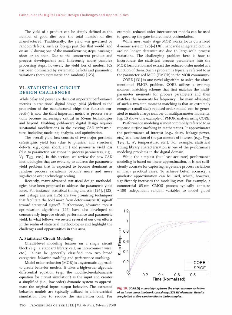
to create behavior models. It takes a high-order algebraic
differential equation (e.g., the modified-nodal-analysis
equation for circuit simulation) as the input and creates
a simplified (i.e., low-order) dynamic system to approxi-
mate the original input–output behavior. The extracted
behavior models are typically utilized in a hierarchical
simulation flow to reduce the simulation cost. For
example, reduced-order interconnect models can be usedto speed up the gate-interconnect cosimulation.
While most early stage MOR works focus on a fixed
dynamic system [128]–[130], nanoscale integrated circuits
are no longer deterministic due to large-scale process
variations. The challenging problem here is how to
incorporate the statistical process parameters into the
MOR formulation and extract the reduced-order model as a
function of them. Such a problem is typically referred to asthe parameterized MOR (PMOR) in the MOR community.
CORE [131] is one novel algorithm to solve the afore-
mentioned PMOR problem. CORE utilizes a two-step
moment matching scheme that first matches the multi-
parameter moments for process parameters and then
matches the moments for frequency. The main advantage
of such a two-step moment matching is that an extremely
compact (small-size) reduced-order model can be gener-ated to match a large number of multiparameter moments.
Fig. 10 shows one example of PMOR analysis using CORE.
Performance modeling is most commonly referred to as
response surface modeling in mathematics. It approximates
the performance of interest (e.g., delay, leakage power,
etc.) as a function of the parameters of interest (e.g., VTH,TOX; L; W, temperature, etc.). For example, statistical
timing library characterization is one of the performancemodeling problems in the digital domain.
While the simplest (but least accurate) performance
modeling is based on linear approximation, it is not suffi-
ciently accurate for capturing large-scale process variations
in many practical cases. To achieve better accuracy, a
quadratic approximation can be used, which, however,
significantly increases the modeling cost. For example, a
commercial 65-nm CMOS process typically contains�100 independent random variables to model global
Fig. 10. CORE [1] accurately captures the step response variation
of an interconnect network containing 1275 RC elements. Results
are plotted at five random Monte Carlo samples.
Calhoun et al.: Digital Circuit Design Challenges and Opportunities
356 Proceedings of the IEEE | Vol. 96, No. 2, February 2008

process variations. In this case, a quadratic model will
include a 100 � 100 quadratic coefficient matrix contain-
ing 104 coefficients. The problem size will become even
larger if device mismatches must be simultaneouslyconsidered.
One successful avenue of attack on this problem relies
on use of projection-based approaches (PROBE [132]) to
address the aforementioned complexity problem. Instead
of fitting the full-rank quadratic model, we attempt to find
an optimal low-rank model by minimizing the approxima-
tion error. For example, using the PROBE method (see
Fig. 11), the number of model coefficients almost linearlyscales with the number of process parameters.
Reducing the size of these models is only one of the
critical optimizations we need to address. Another is the
runtime of some models. A particularly vexing example is
the problem of estimating rare event statistics for high-
replication circuits such as SRAMs and flip-flops. In these
scenarios, a very rare event for a single cell may become a
not-so-rare event for a full SRAM or control-dominatedASIC, where millions of copies of this fundamental circuit
may be present. In these problems, methods borrowed
from data mining turn out to be highly useful. For example,
the method called statistical blockade proposed in [133]
attempts to build a nonlinear classifier that filters out
Binsufficiently rare[ combinations of statistical circuit
parameters during Monte Carlo analysis. The core idea is
quite simple: it is easy to generate the data for one MonteCarlo sample; it is expensive to actually simulate the circuit
associated with each sample. Statistical blockade prevents
us from having to simulate the uninteresting high pro-
bability circuits but passes through the rare event param-
eter combinations. In this way, rare circuit events that
occur far out in low-probability tails of the performance
distribution can be accurately and much more quickly
extracted. The technique can offer significant speedups.For example, a recently proposed analytical model for DRV
was validated with a 1 billion element Bvirtual[ Monte
Carlo analysis: an advanced form of statistical blockade was
applied [134], which required the simulation of only
roughly 45 000 different circuit points to achieve 6-�accuracy, a speedup of over 20 000 times.
B. Statistical Circuit AnalysisIntegrated circuit analysis has been moving from the
traditional corner-based approach towards a range of new
statistical flows for both transistor-level blocks and full-
chip systems.
Direct Monte Carlo analysis based on transistor-levelsimulation is a straightforward yet expensive approach to
estimate the statistical performance distribution. One
more efficient approach is to first extract the performance
model and then estimate the distribution using the model.
In many practical cases, if the performance model is ap-
proximated as a quadratic function, the performance dis-
tribution can be analytically extracted using the APEX
algorithm proposed in [135]. APEX conceptually considersthe unknown probability density function to be of the form
of the impulse response of a linear time-invariant (LTI)
system. The probability density function is then optimally
approximated by moment matching.
An alternative strategy is to better control the Monte
Carlo samples to reduce the analysis cost. Instead of
directly drawing samples from a pseudorandom number
generator, [136] uses so-called low-discrepancy samples,which are deterministically chosen to Bmore uniformly[sample the statistical distribution. The technique, of clas-
sical origin, is called quasi-Monte Carlo (QMC) and, in-
terestingly enough, is now a standard method in the
computational finance world, used for evaluating complex
financial instruments under various forms of statistical
uncertainty. The technique seems extremely promising
when applied to the world of scaled semiconductor prob-lems as well: speedups from 10 to 50 times have been
Fig. 11. PROBE [1] significantly reduces the number of model coefficients compared with the traditional full-rank quadratic approximation.
Calhoun et al.: Digital Circuit Design Challenges and Opportunities
Vol. 96, No. 2, February 2008 | Proceedings of the IEEE 357

demonstrated in [136] compared with the direct MonteCarlo simulation. Fig. 12 shows one detailed example from
statistical SRAM analysis.
Full-chip statistical analysis typically utilizes a hierar-
chical flow to handle the large problem size. For example,
the statistical static timing analysis (SSTA) proposed in
[137] takes the gate-level timing model as the input,
propagates the delay distributions throughout the full-chip
netlist by a number of SUMð�Þ and MAXð�Þ operations,and finally generates the statistical slacks to predict the
parametric timing yield.
While the SSTA algorithm in [137] is limited to linear
approximations, Zhan et al. further proposed an improved
algorithm that can handle nonlinear gate-level timing
models and nonlinear MAXð�Þ approximations [138]; see
Fig. 13. Compared with linear approximations, more than
10x error reduction has been demonstrated in [138] byapplying quadratic models to a number of benchmark
circuits.
In addition to delay variations, leakage power varies
significantly (e.g., 10x � 20x) in nanoscale technologies.
To accurately predict the leakage variation and facilitate an
efficient leakage/timing cooptimization, [139] proposed a
novel projection-based full-chip leakage analysis algo-
rithm. The algorithm can extract quadratic leakage modelsby using an iterative numerical algorithm borrowed from
matrix computations. The extracted leakage power,
therefore, is not limited to a log-normal distribution.
C. Statistical Circuit OptimizationThe objective of statistical circuit optimization is to
leave sufficient performance margins to accommodate
large-scale process variations. The recent advances instatistical circuit analysis make it possible to accurately
predict statistical performance distribution, thereby facil-
itating much more accurate statistical optimization than
the traditional corner-based technique. Overdesign can be
avoided (or at least significantly reduced) by using the
statistical techniques.
Transistor-level statistical optimization focuses on a
single circuit block (e.g., flip flops, memory cells, etc.). Ittakes a fixed circuit topology and optimizes the device sizes
(e.g., transistor widths and lengths) to maximize the per-
formance of interest (e.g., power, delay, etc.). Although
one circuit block is small (e.g., consisting of 10 � 20
transistors), statistically optimizing such a block is not
trivial since its performance can be affected by 50 � 100
process parameters and the variations of these parameters
significantly increase the problem complexity.The ROAD tool developed in [140] is a novel opti-
mization algorithm to address the transistor-level problem.
ROAD consists of three major steps: 1) performance
modeling using PROBE [132]; 2) statistical performance
analysis using APEX [135]; and 3) statistical optimization
to push the distribution tail to the specification boundary.
ROAD utilizes PROBE and APEX for statistical modeling
and analysis so that the optimization problem becomestractable with consideration of all process variations.
Compared with transistor-level optimization, full-chip
statistical optimization is much more challenging due to
the significantly increased problem size. A particularly
fruitful class of methods for these large problems relies on
clever exploitation of convex modeling. One example sta-
tistical technique for optimizing (i.e., sizing) large-size
digital circuits is [141]. The main idea is to approximatethe gate and interconnect delays by (generalized) posy-
nomial functions. As such, the digital sizing problem can
be formulated as a (generalized) geometric programming
that can be efficiently and robustly solved by a convex
optimizer for extremely large problem sizes. In many
practical cases, the approximated polynomial delay models
are sufficiently accurate to create a good initial design
from which further local optimizations can be applied withfast convergence.
VII. MAINTAINING THE DIGITALDESIGN ABSTRACTION ASSCALING CONTINUES
Digital circuit design has the dominant position that it does
because of its ability to hide the many layers of complexphysical and electrical behavior of the elementary devices
it exploits. For example, digital noise margins ensure
predictable behavior according to relatively simple logic-
level abstractions even in the presence of process,
temperature, and voltage variability and increasingly
Bnonideal[ devices. The robustness of these logic-level
abstractions has resulted in entire chip-level design flows
(most notably for ASICs,) which are based on judicioushiding of circuit and layout details. These design flows
have been remarkably successful for the past two decades
but are today under duress due to the challenges arising
from nanometer-scale transistors.
The focus of the design and methodology efforts
described in this paper is to preserve the integrity of these
abstractions and to ensure robust designs while supporting
the additional parameters required for optimal design, astransistors move further in the nanoscale regime.
In this paper, we have considered many of the details
associated with this effort. We can attempt to summarize
these succinctly as follows.
• More aggressive techniques are required to ensure
the electrical robustness of the most important
nets in a digital IC: the clock and power supplies.
• Lithography challenges are forcing more stringentrules and greater regularity into the design flow. To
minimize these so-called systematic variations, IC
designs must be constrained to regular, lithography-
friendly layout patterns in order for designers to
have reasonable control over the precise device
shapes printed in silicon, and thus the behavior of
the devices composed by these printed shapes.
Calhoun et al.: Digital Circuit Design Challenges and Opportunities
358 Proceedings of the IEEE | Vol. 96, No. 2, February 2008
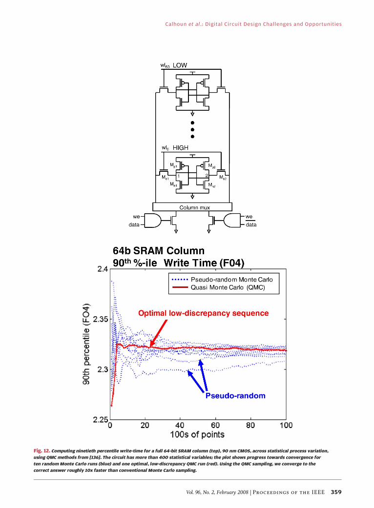
Fig. 12. Computing ninetieth percentile write-time for a full 64-bit SRAM column (top), 90 nm CMOS, across statistical process variation,
using QMC methods from [136]. The circuit has more than 400 statistical variables; the plot shows progress towards convergence for
ten randomMonte Carlo runs (blue) and one optimal, low-discrepancy QMC run (red). Using the QMC sampling, we converge to the
correct answer roughly 10x faster than conventional Monte Carlo sampling.
Calhoun et al.: Digital Circuit Design Challenges and Opportunities
Vol. 96, No. 2, February 2008 | Proceedings of the IEEE 359
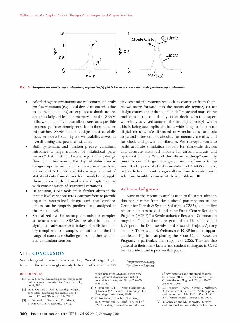
• After lithographic variations are well controlled, truly
random variations (e.g., local device mismatches due
to doping fluctuations) are expected to dominate and
are especially critical for memory circuits. SRAMcells, which employ the smallest transistors possible
for density, are extremely sensitive to these random
mismatches. SRAM circuit designs must carefully
focus on both cell stability and write ability as well as
overall timing and power constraints.
• Both systematic and random process variations
introduce a large number of Bstatistical para-
meters[ that must now be a core part of any designflow. (In other words, the days of deterministic
design steps, or simple worst case corner analysis,
are over.) CAD tools must take a large amount of
statistical data from device-level models and apply
them to circuit-level analysis and optimization
with consideration of statistical variations.
• In addition, CAD tools must further abstract the
circuit-level variations into a compact form to provideinput to system-level design such that variation
effects can be properly predicted and analyzed at
the system level.
• Specialized synthesis/compiler tools for complex
structures such as SRAMs are also in need of
significant advancement; today’s simplistic mem-
ory compilers, for example, do not handle the full
range of nanoscale challenges, from either system-atic or random sources.
VIII. CONCLUSION
Well-designed circuits are one key Binsulating[ layer
between the increasingly unruly behavior of scaled CMOS
devices and the systems we seek to construct from them.
As we move forward into the nanoscale regime, circuit
design comes under duress to Bhide[more and more of the
problems intrinsic to deeply scaled devices. In this paper,we briefly surveyed some of the strategies through which
this is being accomplished, for a wide range of important
digital circuits. We discussed new techniques for basic
logic and interconnect circuits, for memory circuits, and
for clock and power distribution. We surveyed work to
build accurate simulation models for nanoscale devices
and accurate statistical models for circuit analysis and
optimization. The Bend of the silicon roadmap[ certainlypresents a set of large challenges, as we look forward to the
next 10–15 years of (final?) evolution of CMOS circuits,
but we believe circuit design will continue to evolve novel
solutions to address many of these problems. h
Acknowledgment
Most of the circuit examples used to illustrate ideas inthis paper came from the authors’ participation in the
Center for Circuit & System Solutions (C2S2),3 one of five
research centers funded under the Focus Center Research
Program (FCRP),4 a Semiconductor Research Corporation
program. The authors are grateful to D. Radack and
J. Zolper of the Defense Advanced Research Projects Agency
and to S. Thomas and B. Weitzman of FCRP for their support
and leadership in championing the Focus Center ResearchProgram, in particular, their support of C2S2. They are also
grateful to their many faculty and student colleagues in C2S2
for their ideas and inputs on this paper.
REFERENCES
[1] G. E. Moore, BCramming more componentsonto integrated circuits,[ Electronics, vol. 38,no. 8, 1965.
[2] H. S. Lee and C. Sodini, BAnalog-to-digitalconverters: Digitizing the analog world,[Proc. IEEE, vol. 96, no. 2, Feb. 2007.
[3] R. Dennard, F. Gaensslen, V. Rideout,E. Bassous, and A. LeBlanc, BDesign
of ion-implanted MOSFETs with verysmall physical dimensions,[ IEEE J.Solid-State Circuits, vol. 9, pp. 256–268,May 1974.
[4] Y. Taur and T. K. H. Ning, Fundamentalsof Modern VLSI Devices. Cambridge, U.K.:Cambridge Univ. Press, 1998.
[5] T. Skotnicki, J. Hutchby, T.-J. King,H.-S. Wong, and F. Boeuf, BThe end ofCMOS scaling: Toward the introduction
of new materials and structural changesto improve MOSFET performance,[ IEEECircuits Devices Mag., vol. 21, pp. 16–26,Jan./Feb. 2005.
[6] M. Horowitz, E. Alon, D. Patil, S. Naffziger,R. Kumar, and K. Bernstein, BScaling, power,and the future of CMOS,[ in Proc. IEEEInt. Electron Devices Meeting, Dec. 2005.
[7] R. Gonzalez and M. Horowitz, BSupplyand threshold voltage scaling for low power
3http://www.c2s2.org.4http://www.fcrp.org.
Fig. 13. The quadratic MAXð�Þ approximation proposed in [1] yields better accuracy than a simple linear approximation.
Calhoun et al.: Digital Circuit Design Challenges and Opportunities
360 Proceedings of the IEEE | Vol. 96, No. 2, February 2008

CMOS,[ IEEE J. Solid-State Circuits, vol. 32,pp. 1210–1216, Aug. 1997.
[8] V. Zyuban and P. Strenski, BUnifiedmethodology for resolving power-performancetradeoffs at the microarchitectural and circuitlevels,[ in Proc. IEEE Int. Symp. Low-PowerElectron. Design, 2002, pp. 166–171.
[9] V. Zyuban and P. Kogge, BOptimizationof high-performance superscalararchitectures for energy efficiency,[ inProc. Int. Symp. Low-Power Electron.Design, 2000, pp. 84–89.
[10] R. Brodersen, M. Horowitz, D. Markovic,B. Nikolic, and V. Stojanovic, BMethodsfor true power minimization,[ in Proc.ACM/IEEE Int. Conf. Computer-Aided Design,Nov. 2002, pp. 35–42.
[11] A. Chandrakasan, S. Sheng, and R. Brodersen,BLow-power CMOS digital design,[ IEEE J.Solid-State Circuits, vol. 24, no. 4, pp. 473–484,Apr. 1992.
[12] G. Semeraro, G. Magklis, R. Balasubramonian,D. H. Albonesi, S. Dwarkadas, and M. Scott,BEnergy-efficient processor design usingmultiple clock domains with dynamic voltageand frequency scaling,[ in Proc. 8th Int.Symp. High Performance Comput. Arch., 2002,pp. 29–42.
[13] G. Patounakis, Y. Zheng, and K. Shepard,BA fully integrated on-chip dc-dc conversionand power management system,[ IEEE J.Solid-State Circuits, vol. 39, pp. 443–451,Mar. 2004.
[14] J. Tschanz, J. Kao, S. Narendra, R. Nair,D. Antoniadis, A. Chandrakasan, and V. De,BAdaptive body bias for reducing impacts ofdie-to-die and within-die parameter variationson microprocessor,[ IEEE J. Solid-StateCircuits, vol. 37, pp. 1396–1401, Nov. 2002.
[15] C. Kim, D. Burger, and S. Keckler,BNonuniform cache architectures forwire-delay dominated on-chip caches,[IEEE Micro, vol. 23, pp. 99–107,Jun. 2003.
[16] R. Ho, K. Mai, and M. Horowitz, BThe futureof wires,[ Proc. IEEE, vol. 89, pp. 490–504,Apr. 2001.
[17] P. Saxena, N. Menezes, P. Cocchini, andD. Kirkpatrick, BRepeater scaling andits impact on CAD,[ IEEE Trans.Computer-Aided Design Integr. CircuitsSyst., vol. 23, pp. 451–463, Apr. 2004.
[18] R. Ho, K. Mai, and M. Horowitz, BEfficienton-chip global interconnects,[ in Proc. IEEESymp. VLSI Circuits, 2002, pp. 271–274.
[19] D. Schinkel, E. Mensink, E. Klumperink,E. v. Tuijl, and B. Nauta, BA 3 Gb/s/chtransceiver for RC-limited on-chipinterconnects,[ in Proc. IEEE Int. Solid-StateCircuits Conf., Feb. 2005, pp. 386–387.
[20] A. Jose, G. Patounakis, and K. Shepard,BPulsed current-mode signaling for nearlyspeed-of-light intrachip communications,[IEEE J. Solid-State Circuits, vol. 41,pp. 772–780, Apr. 2006.
[21] A. Jose and K. Shepard, BDistributed losscompensation for low-latency on-chipinterconnects,[ in Proc. IEEE Int. Solid StateCircuits Conf., Feb. 2006, pp. 1558–1567.
[22] T. Fischer, F. Anderson, B. Patella, andS. Naffziger, BA 90 nm variable-frequencyclock system for a power-manageditanium-family processor,[ in Proc. IEEEInt. Solid-State Circuits Conf., Feb. 2005,pp. 294–599.
[23] P. J. Restle, T. G. McNamara, D. A. Webber,P. J. Camporese, K. F. Eng, K. A. Jenkins,D. H. Allen, M. J. Rohn, M. P. Quaranta,D. W. Boerstler, C. J. Alpert, C. A. Carter,
R. N. Bailey, J. G. Petrovick, B. L. Krauter,and B. D. McCredie, BA clock distributionnetwork for microprocessors,[ IEEE J.Solid-State Circuits, vol. 36, pp. 792–799,May 2001.
[24] S. Chan, K. Shepard, and P. Restle,BDesign of resonant global clockdistributions,[ in Proc. IEEE Int. Conf.Computer Design, 2003, pp. 238–243.
[25] V. Chi, BSalphasic distribution of clocksignals for synchronous systems,[ IEEETrans. Comput., vol. 43, pp. 597–602,May 1994.
[26] F. O’Mahony, C. Yue, M. Horowitz, andS. Wong, BA 10-GHz global clock distributionusing coupled standing-wave oscillators,[IEEE J. Solid-State Circuits, vol. 38,pp. 1813–1820, Nov. 2003.
[27] J. Wood, T. Edwards, and S. Lipa, BRotarytraveling-wave oscillator array: A newclock technology,[ IEEE J. Solid-StateCircuits, vol. 36, pp. 1654–1665,Nov. 2001.
[28] S. Chan, P. Restle, K. Shepard, N. James, andR. Franch, BA 4.6 GHz resonant global clockdistribution,[ in Proc. IEEE Int. Solid-StateCircuits Conf., Feb. 2004, pp. 342–343.
[29] S. C. Chan, K. L. Shepard, and P. J. Restle,BUniform-phase, uniform-amplitude,resonant-load global clock distributions,[IEEE J. Solid-State Circuits, vol. 40,pp. 102–109, Jan. 2005.
[30] S. Chan, K. Shepard, and P. Restle, B1.1 to1.6 GHz distributed differential oscillatorglobal clock network,[ in Proc. IEEE Int.Solid-State Circuits Conf., Feb. 2005,pp. 518–519.
[31] S. C. Chan, K. L. Shepard, and P. J. Restle,BDistributed differential oscillators for globalclock networks,[ IEEE J. Solid-State Circuits,vol. 41, pp. 2083–2094, Sep. 2006.
[32] R. Ho, B. Amrutur, K. Mai, B. Wilburn,T. Mori, and M. Horowitz, BApplications ofon-chip samplers for test and measurementof integrated circuits,[ in Proc. IEEE Symp.VLSI Circuits, 2002, pp. 138–139.
[33] Y. Zheng and K. Shepard, BOn-chiposcilloscopes for noninvasive time-domainmeasurement of waveforms in digitalintegrated circuits,[ IEEE Trans. VLSI Syst.,vol. 11, pp. 336–344, Mar. 2003.
[34] E. Alon, V. Stojanovic, and M. Horowitz,BCircuits and techniques for high-resolutionmeasurement of on-chip power supplynoise,[ IEEE J. Solid-State Circuits, vol. 40,pp. 820–829, Apr. 2005.
[35] S. Rajapandian, Z. Xu, and K. Shepard,BImplicit DC-DC downconversion throughcharge-recycling,[ IEEE J. Solid-State Circuits,vol. 40, pp. 846–852, Apr. 2005.
[36] S. Rajapandian, K. Shepard, P. Hazucha, andT. Karnik, BHigh-voltage power deliverythrough charge recycling,[ IEEE J. Solid-StateCircuits, vol. 41, pp. 1400–1410, Jun. 2006.
[37] W. Zhao and Y. Cao. (2006, Nov.).New generation of predictive technologymodel for sub-45 nm early designexploration. IEEE Trans. Electron Devices[Online]. 53, pp. 2816–2823. Available:http://www.eas.asu.edu/~ptm
[38] L. Chang, Y. K. Choi, S. Ha, P. Ranade,S. Ziong, J. Bokor, C. Hu, and T. J. King,BExtremely scaled silicon nano-CMOSdevices,[ Proc. IEEE, vol. 91, pp. 1860–1873,Nov. 2003.
[39] N. Mohta and S. E. Thompson, BMobilityenhancement: The next vector to extendMoore’s law,[ IEEE Circuits Devices Mag.,vol. 21, no. 5, pp. 18–23, Sep./Oct. 2005.
[40] A. Khakifirooz and D. Antoniadis,BTransistor performance scaling: The roleof virtual source velocity and its mobilitydependence,[ in Proc. IEEE Int. ElectronDevices Meeting, Dec. 2006, pp. 667–670.
[41] M. Lundstrom, BDevice physics at the scalinglimit: What matters?[ in Proc. IEEE Int.Electron Devices Meeting, Dec. 2003,pp. 789–792.
[42] M. V. Dunga, C. H. Lin, X. Xi, D. D. Lu,A. M. Niknejad, and C. Hu, BModelingadvanced FET technology in a compactmodel,[ IEEE Trans. Electron Devices,vol. 53, pp. 1971–1978, Sep. 2006.
[43] C. Leroux, J. Mitard, G. Ghibaudo, X. Garros,G. Reimbold, B. Guillaumot, and F. Martin,BCharacterization and modeling of hysteresisphenomena in high-k dielectrics,[ in Proc.IEEE Int. Electron Devices Meeting,Dec. 2004, pp. 737–740.
[44] A. E. Islam, G. Gupta, S. Mahapatra,A. T. Krishnan, K. Ahmed, F. Nouri,A. Oates, and M. A. Alam, BGate leakagevs. NBTI in plasma nitrided oxides:Characterization, physical principles, andoptimization,[ in Proc. IEEE Int. ElectronDevices Meeting, Dec. 2006, pp. 329–332.
[45] S. Bhardwaj, W. Wang, R. Vattikonda,Y. Cao, and S. Vrudhula, BPredictivemodeling of the NBTI effect for reliabledesign,[ in Proc. IEEE Custom Integr.Circuits Conf., Sep. 2006, pp. 189–192.
[46] X. Huang, W. C. Lee, C. Kuo, D. Hisamoto,L. Chang, and J. Kedzierski, BSub-50 nmFinFET: PFET,[ in Proc. IEEE Int. ElectronDevices Meeting, Dec. 2003, pp. 679–682.
[47] W. Zhao and Y. Cao, BPredictive technologymodel for nano-CMOS design exploration,[ACM J. Emerging Technol. Comput. Syst.,vol. 3, no. 1, pp. 1–17, Apr. 2007.
[48] J. G. Fossum, M. M. Chowdhury,V. P. Trivedi, T.-J. King, Y.-K. Choi, J. An,and B. Yu, BPhysical insights on designand modeling of nanoscale FinFETs,[ inProc. IEEE Int. Electron Devices Meeting,Dec. 2003, pp. 679–682.
[49] B. Iniguez, T. A. Fjeldly, A. Lazaro,F. Danneville, and M. J. Deen,BCompact-modeling solutions fornanoscale double-gate and gate-all-aroundMOSFETs,[ IEEE Trans. Electron Devices,vol. 53, pp. 2128–2142, Sep. 2006.
[50] G. Gildenblat, X. Li, W. Wu, H. Wang,A. Jha, A. R. Van Langevelde, G. D. J. Smit,A. J. Scholtena, and D. B. M. Klaassen,BPSP: An advanced surface-potential-basedMOSFET model for circuit simulation,[IEEE Trans. Electron Devices, vol. 53,pp. 1979–1993, Sep. 2006.
[51] C.-H. Lin, X. Xi, J. He, L. Chang, R. Q.Williams,M. B. Ketchen, W. E. Haensch, M. Dunga,S. Balasubramanian, A.M.Niknejad,M. Chan,and C. Hu, BCompact modeling of FinFETsfeaturing in independent-gate operationmode,[ in Proc. IEEE Int. Symp. VLSI Technol.,Syst., Applicat., 2005, pp. 120–121.
[52] S. Borkar, T. Karnik, S. Narendra, J. Tschanz,A. Keshavarzi, and V. De, BParametervariations and impact on circuits andmicroarchitecture,[ in Proc. ACM/IEEEDesign Automation Conf., Jun. 2003,pp. 338–342.
[53] S. R. Nassif, N. Hakim, and D. Boning, BThecare and feeding of your statistical statictimer,[ in Proc. ACM/IEEE Int. Conf.Computer-Aided Design, Nov. 2004,pp. 138–139.
[54] S. K. Springer, S. Lee, N. Lu, E. J. Nowak,J.-O. Plouchart, J. S. Wattsa, R. O. Williams,and N. Zamdmer, BModeling of variation in
Calhoun et al.: Digital Circuit Design Challenges and Opportunities
Vol. 96, No. 2, February 2008 | Proceedings of the IEEE 361

submicrometer CMOS ULSI technologies,[IEEE Trans. Electron Devices, vol. 53,pp. 2168–2006, Sep. 2006.
[55] S. R. Nassif, BModel to hardware matchingfor nano-meter scale technologies,[ in Proc.IEEE Int. Symp. Low-Power Electron. Design,2006, pp. 203–206.
[56] M. Chen, W. Zhao, F. Liu, and Y. Cao,BFast statistical circuit analysis withfinite-point based transistor model,[ inProc. Design, Automat. Test Eur. Conf.,Apr. 2007, pp. 1391–1396.
[57] W.-K. Chen, Linear Networks and Systems.Belmont, CA: Wadsworth, 1993,pp. 123–135.
[58] H. Poor, An Introduction to SignalDetection and Estimation. New York:Springer-Verlag, 1985, ch. 4.
[59] K. Itoh, M. Horiguchi, and T. Kawahara,BUltra-low voltage nano-scale embeddedRAMs,[ in Proc. IEEE Int. Symp. Circuits Syst.,2006, pp. 245–248.
[60] A. Bhavnagarwala, A. Kapoor, and J. Meindl,BDynamic-threshold CMOS SRAM cellsfor fast, portable applications,[ in Proc.IEEE Int. ASIC/SOC Conf., Sep. 2000,pp. 359–363.
[61] H. Kawaguchi, Y. Itaka, and T. Sakurai,BDynamic cut-off scheme for low-voltageSRAM’s,[ in Proc. IEEE Symp. VLSI Circuits,Jun. 1998, pp. 140–141.
[62] K. Kouichi, M. Takayuki, M. Kyeong-Sik, andS. Takayasu, BTwo orders of magnitudeleakage power reduction of low voltageSRAM’s by row-by-row dynamic VDDcontrol (RRDV) scheme,[ in Proc.IEEE Int. ASIC/SOC Conf., Sep. 2002,pp. 381–385.
[63] A. Bhavnagarwala, S. V. Kosonocky,S. P. Kowalczyk, R. V. Joshi, Y. H. Chan,U. Srinivasan, and J. K. Wadhwa,BA transregional CMOS SRAM withsingle, logic VDD and dynamic powerrails,[ in Proc. IEEE Symp. VLSI Circuits,Jun. 2004, pp. 292–293.
[64] N. Kim, K. Flautner, D. Blaauw, and T.Mudge,BCircuit and microarchitectural techniquesfor reducing cache leakage power,[IEEE Trans. VLSI Syst., vol. 12, pp. 167–184,Feb. 2004.
[65] H. Qin, Y. Cao, D. Markovic, A. Vladimirescu,and J. Rabaey, BSRAM leakage suppression byminimizing standby supply voltage,[ in Proc.IEEE Int. Symp. Quality Electronic Design(ISQED), Mar. 2004, pp. 55–60.
[66] H. Yamauchi, T. Iwata, H. Akamatsu, andA. Matsuzawa, BA 0.8 V/100 MHz/sub-5 mW-operated mega-bit SRAM cellarchitecture with charge-recycle offset-sourcedriving (OSD) scheme,[ in Proc. IEEE Symp.VLSI Circuits, Jun. 1996, pp. 126–127.
[67] K. Osada, Y. Saitoh, E. Ibe, and K. Ishibashi,B16.7-fA/Cell tunnel-leakage-suppressed16-mb SRAM for handling cosmic-ray-induced multierrors,[ IEEE J. Solid-StateCircuits, vol. 38, pp. 1952–1957,Nov. 2003.
[68] K. Zhang, U. Bhattacharya, Z. Chen,F. Hamzaoglu, D. Murray, N. Vallepalli,Y. Yang, B. Zheng, and M. Bohr,BA SRAM Design on 65 nm CMOStechnology with integrated leakagescheme,[ in Proc. IEEE Symp. VLSICircuits, Jun. 2004, pp. 294–295.
[69] K. Nii, Y. Tsukamoto, T. Yoshizawa,S. Imaoka, and H. Makino, BA 90 nmDual-Port SRAM with 2.04 �m 2 8T-thincell using dynamically-controlled columnbias scheme,[ in Proc. IEEE Int. Solid-StateCircuits Conf., Feb. 2004, pp. 508–509.
[70] A. Agarwal, H. Li, and K. Roy, BA single-Vtlow-leakage gated-ground cache for deepsubmicron,[ IEEE J. Solid-State Circuits,vol. 38, pp. 319–328, Feb. 2003.
[71] T. Enomoto, Y. Oka, and H. Shikano,BA self-controllable voltage level (SVL)circuit and its low-power high-speedCMOS circuit applications,[ IEEE J.Solid-State Circuits, vol. 38, pp. 1220–1226,Jul. 2003.
[72] J. Wang and B. Calhoun, BCanary replicafeedback for near-DRV standby VDDscaling in a 90 nm SRAM,[ in Proc.IEEE Custom Integr. Circuits Conf. (CICC),Sep. 2007.
[73] E. Seevinck, F. List, and J. Lohstroh,BStatic noise margin analysis of MOS SRAMcells,[ IEEE J. Solid-State Circuits, vol. SC-22,pp. 748–754, Oct. 1987.
[74] B. H. Calhoun and A. Chandrakasan,BAnalyzing static noise margin forsubthreshold SRAM in 65 nm CMOS,[ inProc. Eur. Solid-State Circuits Conf.,Sep. 2005, pp. 363–366.
[75] B. H. Calhoun and A. Chandrakasan,BA 256 kb sub-threshold SRAM in 65 nmCMOS,[ in Proc. IEEE Int. Solid-State CircuitsConf., Feb. 2006, pp. 628–629.
[76] A. Bhavnagarwala, S. Kosonocky, C. Radens,K. Stawiasz, R. Mann, Q. Ye, and K. Chin,BFluctuation limits and scaling opportunitiesfor CMOS SRAM cells,[ in Proc. IEEEElectron. Device Meeting, Dec. 2005,pp. 659–662.
[77] K. Takeda, Y.Hagihara, Y. Aimoto,M.Nomura,Y. Nakazawa, T. Ishii, and H. Kobatake,BA read-static-noise-margin-free sram cell forlow-Vdd and high-speed applications,[ in Proc.IEEE Int. Solid-State Circuits Conf., Feb. 2005,pp. 478–479.
[78] M. Khellah, Y. Ye, N. S. Kim, D. Somasekhar,G. Pandya, A. Farhang, K. Zhang, C. Webb,and V. De, BWordline and bitline pulsingschemes for improving SRAM cell stability inlow-Vcc 65 nmCMOS designs,[ in Proc. IEEESymp. VLSI Circuits, Jun. 2006.
[79] Y. Morita, H. Fujiwara, H. Noguchi,K. Kawakami, J. Miyakoshi, S. Mikami,K. Nii, H. Kawaguchi, and M. Yoshimoto,BA Vth-variation-tolerant SRAM with0.3-V minimum operation voltage formemory-rich SoC under DVS environment,[in Proc. IEEE Symp. VLSI Circuits, Jun. 2006,pp. 13–14.
[80] S. Ohbayashi, M. Yabuuchi, K. Nii,Y. Tsukamoto, S. Imaoka, Y. Oda, M. Igarashi,M. Takeuchi, H. Kawashima, H. Makino,Y. Yamaguchi, K. Tsukamoto, M. Inuishi,K. Ishibashi, and H. Shinohara, BA 65 nmSoC embedded 6T-SRAM design formanufacturing with read and write cellstabilizing circuits,[ in Proc. IEEE Symp.VLSI Circuits, Jun. 2006, pp. 16–17.
[81] T. Suzuki, H. Yamauchi, Y. Yamagami,K. Satomi, and H. Akamatsu, BA stableSRAM cell design against simultaneouslyR/W disturbed accesses,[ in Proc. IEEE Symp.VLSI Circuits, 2006, pp. 11–12.
[82] K. Agawa, H. Hara, T. Takayanagi, andT. Kuroda, BA bitline leakage compensationscheme for low-voltage SRAMs,[ IEEE J.Solid-State Circuits, vol. 36, pp. 726–734,May 2001.
[83] Z. Guo, S. Balasubramanian, R. Zlatanovici,T.-J. King, and B. Nikolic, BFinFET-basedSRAM design,[ in Proc. IEEE Int. Symp. LowPower Electron. Design, Aug. 2005, pp. 2–7.
[84] T. Fukuda, S. Hayakawa, andN. Shigyo, BAlpha and neutron SER ofembedded-SRAM and novel estimation
method,[ in Proc. Int. Symp. Automat.Test, Apr. 2006, pp. 1–3.
[85] P. Hazucha, T. Karnik, J. Maiz, S. Walstra,B. Bloechel, J. Tschanz, G. Dermer,S. Hareland, P. Armstrong, andS. Borkar, BNeutron soft error ratemeasurements in a 90-nm CMOSprocess and scaling trends in SRAMfrom 0.25-�m to 90-nm generation,[ inProc. IEEE Int. Electron Devices Meeting,Dec. 2003, pp. 21.5.1–21.5.4.
[86] M. Agostinelli, J. Hicks, J. Xu, B. Woolery,K. Mistry, K. Zhang, S. Jacobs, J. Jopling,W. Yang, B. Lee, T. Raz, M. Mehalel,P. Kolar, Y. Wang, J. Sandford, D. Pivin,C. Peterson, M. DiBattista, S. Pae,M. Jones, S. Johnson, and G. Subramanian,BErratic fluctuations of SRAM cacheVmin at the 90 nm process technologynode,[ in Proc. IEEE Int. Electron DevicesMeeting, Dec. 2005, pp. 655–658.
[87] S. Mukhopadhyay, K. Kim, H. Mahmoodi,and K. Roy, BDesign of a process variationtolerant self-repairing SRAM for yieldenhancement in nanoscaled CMOS,[IEEE J. Solid-State Circuits, vol. 42,pp. 1370–1382, Jun. 2007.
[88] K.-L. J. Wong and C.-K. Yang, BOffsetcompensation in comparators withminimum input-referred supply noise,[IEEE J. Solid State Circuits, vol. 39,pp. 837–840, May 2004.
[89] K. Ishibashi, K. Takasugi, K. Komiyaji,H. Toyoshima, T. Yamanaka, A. Fukami,N. Hashimoto, N. Ohki, A. Shimizu,T. Hashimoto, T. Nagano, andT. Nishida, BA 6-ns 4-Mb CMOSSRAM with offset-voltage-insensitivecurrent sense amplifiers,[ IEEE J.Solid-State Circuits, vol. 30, pp. 480–486,Apr. 1995.
[90] B. Amrutur and M. Horowitz, BA replicatechnique for wordline and sensecontrol in low-power SRAMs,[ IEEE J.Solid-State Circuits, vol. 33, pp. 1208–1219,Aug. 1998.
[91] T. Chappell, B. A. Chappell, S. E. Schuster,J. W. Allan, S. P. Klepner, R. V. Joshi, andR. L. Franch, BA 2-ns cycle, 3.8 ns access512 kb CMOS ECL SRAM with a fullypipelined architecture,[ IEEE J. Solid-StateCircuits, vol. 26, pp. 1577–1585, Nov. 1991.
[92] BPanel: Soft error scaling trends,[ in Proc.2nd Workshop Syst. Effects Logic Soft Errors,Apr. 2006. [Online]. Available: http://www.selse.org/selse2.org.
[93] J. F. Ziegler, BTerrestrial cosmic rays,[ IBM J.Res. Develop., vol. 40, no. 1, pp. 19–39,Jan. 1996.
[94] F. A. Bower, S. Ozev, and D. J. Sorin,BAutonomic microprocessor execution viaself-repairing arrays,[ IEEE Trans. Depend.Secure Comput., vol. 2, pp. 297–310,Oct.–Dec. 2005.
[95] F. A. Bower, D. Sorin, and S. Ozev,BA mechanism for online diagnosisof hard faults in microprocessors,[ inProc. 38th IEEE/ACM Int. Symp.Microarchitect., Nov. 2005, pp. 197–208.
[96] J. Srinivasan, S. V. Adve, P. Bose, andJ. A. Rivers, BThe impact of technologyscaling on lifetime reliability,[ in Proc. Int.Conf. Depend. Syst. Networks, Jun. 2004,pp. 177–186.
[97] A. Agarwal, B. C. Paul, S. Mukhopadhyay,and K. Roy, BProcess variation in embeddedmemories: Failure analysis and variationaware architecture,[ IEEE J. Solid-StateCircuits, vol. 40, pp. 1804–1814,Sep. 2005.
Calhoun et al.: Digital Circuit Design Challenges and Opportunities
362 Proceedings of the IEEE | Vol. 96, No. 2, February 2008
[98] M. Spica and T. M. Mak, BDo we needanything more than single bit errorcorrection (ECC)?[ in Proc. IEEE Int.Workshop Memory Technol., Design Testing,Aug. 2004, pp. 111–116.
[99] C. H. Stapper and H.-S. Lee, BSynergisticfault-tolerance for memory chips,[ IEEETrans. Comput., vol. 41, pp. 1078–1087,Sep. 1992.
[100] B. S. Amrutur and M. A. Horowitz,BSpeed and power scaling of SRAM’s,[IEEE J. Solid-State Circuits, vol. 35,pp. 175–185, Feb. 2000.
[101] J. Mitchell, D. Henderson, and G. Ahrens.(2005, Oct.). BIBM Power5 processor-basedservers: A highly available design forbusiness-critical applications,[ in IBM WhitePaper. [Online]. Available: http://www-03.ibm.com/systems/p/hardware/whitepapers/power5_ras.pdf.
[102] S. Rusu, H. Muljono, and B. Cherkauer,BItanium2 processor 6M: Higherfrequency and larger L3 cache,[IEEE Micro, vol. 24, no. 2, pp. 10–18,Mar.–Apr. 2004.
[103] D. K. Bhavsar, BAn algorithm forrow-column self-repair of RAMsand its implementation in the Alpha21264,[ in Proc. Int. Test Conf., Sep. 1999,pp. 311–318.
[104] R. Kanj, R. Joshi, and S. Nassif, BMixtureimportance sampling and its applicationto the analysis of SRAM designs in thepresence of rare failure events,[ inProc. ACM/IEEE Design Automat. Conf.,Jun. 2006.
[105] N. J. Wang and S. J. Patel, BReStore:Symptom-based soft error detectionin microprocessors,[ IEEE Trans.Depend. Secure Comput., vol. 3, no. 3,Jul.–Sep. 2006.
[106] T. Calin, M. Nicolaidis, and R. Velaco,BUpset hardened memory design forsubmicron CMOS technology,[ IEEETrans. Nucl. Sci., vol. 43, pp. 2874–2878,Dec. 1996.
[107] M. Zhang, S. Mitra, T. M. Mak, N. Seifert,N. Wang, Q. Shi, K. S. Kim, N. Shanbhag,and S. Patel, BSequential element designwith built-in soft error resilience,[ IEEETrans. VLSI Syst., vol. 14, pp. 1368–1378,Dec. 2006.
[108] R. Adams, High Performance MemoryTesting: Design Principles, Fault Modelingand Self-Test. Berlin, Germany: Springer,2002.
[109] S. Hamdioui and G. Gaydadjiev, BFuturechallenges in memory testing,[ in Proc.ProRISC, 2003.
[110] L. W. Liebmann, A. Barish, Z. Baum,H. Bonges, S. Bukofsky, C. Fouseca,S. Halle, G. Northrop, S. Runyon, andL. Sigal, BHigh, performance circuitdesign for the RET-enabled 65 nmtechnology node,[ in Proc. SPIE DesignProcess Integr. Microelectron. Manufact. II,L. W. Liebmann, Ed., 2004, vol. 5379,pp. 20–29.
[111] V. Kheterpal, T. Hersan, V. Rovner,D. Motiani, Y. Takagawa, L. Pileggi, andA. Strojwas, BDesign methodology forIC manufacturability based on regularlogic-bricks,[ in Proc. ACM/IEEE DesignAutomat. Conf., Jun. 2005, pp. 353–358.
[112] L. Pileggi and A. J. Strojwas, BRegular fabricsfor nano-scaled CMOS technologies,[ inProc. IEEE Int. Solid State Circuits Conf.,Feb. 2006.
[113] T. Okamoto, T. Kimoto, and N. Maeda,BDesign methodology and tools for NEC
electronics’ structured ASIC ISSP,[ in Proc.ACM Int. Symp. Phys. Design, Apr. 2004,pp. 90–96.
[114] D. Sherlekar, BDesign considerations forregular fabrics,[ in Proc. ACM Int. Symp.Phys. Design, Apr. 2004, pp. 97–102.
[115] K.-C. Wu and Y.-W. Tsai, BStructuredASIC, evolution or revolution?[ in Proc.ACM Int. Symp. Phys. Design, Apr. 2004,pp. 103–106.
[116] L. Capodieci, P. Gupta, A. B. Kahng,D. Sylvester, and J. Yang, BToward amethodology for manufacturability-drivendesign rule exploration,[ in Proc. ACM/IEEEDesign Automat. Conf., Jun. 2004,pp. 311–316.
[117] M. Lavin, F. L. Heng, and G. Northrop,BBackend CAD flows for Frestrictive designrules_,[ in Proc. ACM/IEEE Int. Conf.Computer-Aided Design, Nov. 2004,pp. 739–746.
[118] J. Wang, A. K. Wong, and E. Y. Lam,BPerformance optimization for gridded-layout standard cells,[ in Proc. SPIE 24thAnnu. BACUS Symp. Photomask Technol.,W. Staud and J. T. Weed, Eds., 2004,vol. 5567, pp. 107–118.
[119] T. Jhaveri, L. Pileggi, V. Rovner, andA. J. Strojwas, BMaximization of layoutprintability/manufacturability by extremelayout regularity,[ in Proc. SPIE DesignProcess Integr. Microelectron. Manufact. IV,A. K. K. Wong and V. K. Singh, Eds., 2006,vol. 6156, pp. 67–81.
[120] K. Y. Tong, V. Kheterapal, S. Rovner,H. Schmit, L. Pileggi, and R. Puri, BRegularlogic fabrics for a via patterned gate array(VPGA),[ in Proc. IEEE Custom Integr.Circuits Conf., Sep. 2003, pp. 53–56.
[121] L. Pileggi, H. Schmit, A. J. Strojwas,P. Gopalakrishnan, V. Kheterpal,A. Koorapaty, C. Patel, V. Rovner, andK. Y. Tong, BExploring regular fabrics tooptimize the performance-cost trade-off,[ inProc. ACM/IEEE Design Automat. Conf.,Jun. 2003, pp. 782–787.
[122] Y. Ran and M. Marek-Sadowska, BOndesigning via-configurable cell blocks forregular fabrics,[ in Proc. ACM/IEEE DesignAutomat. Conf., Jun. 2004, pp. 198–203.
[123] P. T. Patel. (2005, Nov.). Yield challengesrequire new DFM approach. EE Times 21.[Online]. Available: http://www.eet.com/news/design/showArticle.jhtml?articleID=174400375
[124] H. Chang and S. Sapatnekar, BStatisticaltiming analysis under spatial correlations,[IEEE Trans. Computer-Aided Design Integr.Circuits Syst., vol. 24, pp. 1467–1482,Sep. 2005.
[125] C. Visweswariah, K. Ravindran, K. Kalafala,S. Walker, S. Narayan, D. Beece, J. Piaget,N. Venkateswaran, and J. Hemmett,BFirst-order incremental block-basedstatistical timing analysis,[ IEEE Trans.Computer-Aided Design Integr. Circuits Syst.,vol. 25, pp. 2170–2180, Oct. 2006.
[126] A. Srivastava, S. Shah, K. Agarwal,D. Sylvester, D. Blaauw, and S. Director,BAccurate and efficient gate-level parametricyield estimation considering correlatedvariations in leakage power andperformance,[ in Proc. ACM/IEEE DesignAutomat. Conf., Jun. 2005, pp. 535–540.
[127] M. Mani, A. Devgan, and M. Orshansky,BAn efficient algorithm for statisticalminimization of total power under timingyield constraints,[ in Proc. ACM/IEEEDesign Automat. Conf., Jun. 2005,pp. 309–314.
[128] L. Pillage and R. Rohrer, BAsymptoticwaveform evaluation for timing analysis,[IEEE Trans. Computer-Aided Design Integr.Circuits Syst., vol. 9, pp. 352–366,Apr. 1990.
[129] A. Odabasioglu, M. Celik, and L. Pileggi,BPRIMA: Passive reduced-orderinterconnect macromodeling algorithm,[IEEE Trans. Computer-Aided Design Integr.Circuits Syst., vol. 17, pp. 645–654,Aug. 1998.
[130] J. Phillips, L. Daniel, and L. Silveira,BGuaranteed passive balancingtransforms for model order reduction,[IEEE Trans. Computer-Aided Design Integr.Circuits Syst., vol. 22, pp. 1027–1041,Aug. 2003.
[131] X. Li, P. Li, and L. Pileggi, BParameterizedinterconnect order reduction withexplicit-and-implicit multi-parametermoment matching for inter/intra-dievariations,[ in Proc. ACM/IEEE Int.Conf. Computer-Aided Design, Nov. 2005,pp. 806–812.
[132] X. Li, J. Le, L. Pileggi, and A. Strojwas,BProjection-based performance modelingfor inter/intra-die variations,[ in Proc.ACM/IEEE Int. Conf. Computer-Aided Design,Nov. 2005, pp. 721–727.
[133] A. Singhee and R. Rutenbar, BStatisticalblockade: A novel method for very fastMonte Carlo simulation of rare circuitevents, and its application,[ in Proc.Design, Automat. Test Eur., Apr. 2007,pp. 1379–1384.
[134] J. Wang, A. Singhee, R. A. Rutenbar, andB. H. Calhoun, BModeling the minimumstandby supply voltage of a full SRAMarray column,[ in Proc. Eur. SolidState Circuits Conf. (ESSCIRC),Sep. 2007.
[135] X. Li, J. Le, P. Gopalakrishnan, and L. Pileggi,BAsymptotic probability extraction fornon-normal distributions of circuitperformance,[ in Proc. ACM/IEEE Int.Conf. Computer-Aided Design, Nov. 2004,pp. 2–9.
[136] A. Singhee and R. Rutenbar, BFromfinance to flip flops: A study of fastquasi-Monte Carlo methods fromcomputational finance applied to statisticalcircuit analysis,[ in Proc. IEEE Int. Symp.Quality Electron. Design, Mar. 2007,pp. 685–692.
[137] J. Le, X. Li, and L. Pileggi, BSTAC: Statisticaltiming analysis with correlation,[ in Proc.ACM/IEEE Design Automat. Conf., Jun. 2004,pp. 343–348.
[138] Y. Zhan, A. Strojwas, X. Li, L. Pileggi,D. Newmark, and M. Sharma,BCorrelation aware statistical timinganalysis with non-Gaussian delaydistributions,[ in Proc. ACM/IEEEDesign Automat. Conf., Jun. 2005,pp. 77–82.
[139] X. Li, J. Le, and L. Pileggi, BProjection-basedstatistical analysis of full-chip leakagepower with non-log-normal distributions,[in Proc. ACM/IEEE Design Automat. Conf.,Jun. 2006, pp. 103–108.
[140] X. Li, P. Gopalakrishnan, Y. Xu, andL. Pileggi, BRobust analog/RF circuitdesign with projection-based posynomialmodeling,[ in Proc. ACM/IEEE Int.Conf. Computer-Aided Design, Nov. 2004,pp. 855–862.
[141] S. Boyd, S. Kim, D. Patil, and M. Horowitz,BDigital circuit optimization via geometricprogramming,[ Oper. Res., vol. 53, no. 6,pp. 899–932, Nov.–Dec. 2005.
Calhoun et al.: Digital Circuit Design Challenges and Opportunities
Vol. 96, No. 2, February 2008 | Proceedings of the IEEE 363

ABOUT THE AUTHORS
Benton H. Calhoun (Member, IEEE) received the
B.S. degree from the University of Virginia,
Charlottesville, and the M.S. and Ph.D. degrees
from the Massachusetts Institute of Technology,
Cambridge, in 2000, 2002, and 2006, respectively,
all in electrical engineering.
In January 2006, he joined the Faculty of the
University of Virginia as an Assistant Professor in
the Electrical and Computer Engineering Depart-
ment. His research interests include low-power
digital circuit design, subthreshold digital circuits, SRAM design for end-
of-the-roadmap silicon, variation-tolerant circuit design methodologies,
and low-energy electronics for medical applications. He is coauthor of
Sub-threshold Design for Ultra Low-Power Systems (Berlin, Germany:
Springer, 2006). He is on the Technical Program Committee for the
International Symposium on Low Power Electronics and Design.
Yu Cao (Member, IEEE) received the B.S. degree in
physics from Peking University, China, in 1996 and
the M.A. degrees in biophysics and the Ph.D.
degree in electrical engineering from the Univer-
sity of California, Berkeley, in 1999 and 2002,
respectively.
After working as a Postdoctoral Researcher
with the Berkeley Wireless Research Center
(BWRC), he joined Arizona State University,
Tempe, where he is now an Assistant Professor
of electrical engineering. He has published numerous articles and
coauthored one book on nano-CMOS physical and circuit design. He
research interests include modeling and analysis of nanoscale CMOS
circuits, physical-level design and tools for variability and reliability, and
reliable integration of postsilicon technologies. He currently serves on
the Technical Program Committee of numerous design automation and
circuit design conferences.
Dr. Cao was received the 2007 Best Paper Award from the
International Symposium on Low Power Electronics and Design, the
2006 National Science Foundation CAREER Award, the 2006 and 2007
IBM Faculty Award, the 2004 Best Paper Award at International
Symposium on Quality Electronic Design, and the 2000 Beatrice Winner
Award at International Solid-State Circuits Conference.
Xin Li (Member, IEEE) received the B.S. and M.S.
degrees in electronics engineering from Fudan
University, Shanghai, China, in 1998 and 2001,
respectively, and the Ph.D. degree in electrical and
computer engineering from Carnegie–Mellon Uni-
versity, Pittsburgh, PA, in 2005.
He is currently a Research Scientist in the
Department of Electrical and Computer Engineer-
ing, Carnegie–Mellon University. He was a summer
Intern with Extreme DA, Palo Alto, CA, in 2004. In
2005, he cofounded Xigmix Inc., a startup company in Pittsburgh to
commercialize his Ph.D. research. He was Chief Technical Officer until the
company was acquired by Extreme DA in 2007. His research interests
include modeling, simulation, and synthesis for analog/RF and digital
systems.
Dr. Li served on the IEEE Outstanding Young Author Award Selection
Committee in 2006. He received the Best Session Award from the
Semiconductor Research Corporation Student Symposium in 2006, the
Best Paper Nomination from the Design Automatic Conference in 2006,
and the IEEE/ACMWilliam J. McCalla ICCAD Best Paper Award in 2004. He
also received the Inventor Recognition Awards from Microelectronics
Advanced Research Corporation in 2006 and 2007.
Ken Mai (Member, IEEE) received the B.S., M.S.,
and Ph.D. degrees in electrical engineering from
Stanford University, Stanford, CA, in 1993, 1997,
and 2005, respectively.
His research interests include high-speed
circuit design, secure IC design, reconfigurable
computing, and computer architecture. He joined
theFaculty of Carnegie–MellonUniversity, Pittsburgh,
PA, in January 2005 as an Assistant Professor in the
Electrical and Computer Engineering Department.
Lawrence T. Pileggi (Fellow, IEEE) received the
Ph.D. degree in electrical and computer engineer-
ing from Carnegie–Mellon University, Pittsburgh,
PA, in 1989.
He is the Tanoto Professor of Electrical and
Computer Engineering at Carnegie–Mellon Uni-
versity. His career began as an IC Designer with
Westinghouse Research, where he was recognized
with the corporation’s highest engineering
achievement award. He began his academic career
at the University of Texas at Austin. In 1995, he joined the Faculty of
Carnegie–Mellon University. His research interests include various
aspects of digital and analog design and design methodologies, where
he has published various papers and received several patents and awards
for his work. He has served as a Consultant and Technical Advisory Board
member for various companies. He helped to start Extreme Design
Automation, Fabbrix, and Xigmix.
Rob A. Rutenbar (Fellow, IEEE) received the
Ph.D. degree from the University of Michigan,
Ann Arbor, in 1984.
He joined the Faculty of Carnegie–Mellon
University, Pittsburgh, PA, where he currently
holds the Stephen Jatras Chair in Electrical and
Computer Engineering. He has worked on tools for
custom circuit synthesis and optimization for
more than 20 years. In 1998, he cofounded
Neolinear Inc. to commercialize the first practical
synthesis tools for analog designs. He was Neolinear’s Chief Scientist
until its acquisition by Cadence in 2004. He is the founding Director of the
U.S. national Focus Research Center for Circuit and System Solutions
(C2S2), a consortium of 17 U.S. universities and more than 50 faculty
funded by the U.S. semiconductor industry and U.S. government to
address future circuit challenges. His work has been featured in venues
ranging from EETimes to the Economist magazine.
Prof. Rutenbar has received many awards over his career. He was a
2001 recipient of the Semiconductor Research Corporation Aristotle
Award for excellence in education and 2007 IEEE Circuits and Systems
Industrial Pioneer Award. He received the 2002 University of Michigan
Alumni Merit Award for Electrical Engineering.
Calhoun et al.: Digital Circuit Design Challenges and Opportunities
364 Proceedings of the IEEE | Vol. 96, No. 2, February 2008
Kenneth L. Shepard (Senior Member, IEEE)
received the B.S.E. degree from Princeton Univer-
sity, Princeton, NJ, in 1987 and the M.S. and Ph.D.
degrees in electrical engineering from Stanford
University, Stanford, CA, in 1988 and 1992,
respectively.
From 1992 to 1997, he was a Research Staff
Member and Manager with the VLSI Design
Department, IBM T. J. Watson Research Center,
Yorktown Heights, NY, where he was responsible
for the design methodology for IBM’s G4 S/390 microprocessors. Since
1997, he has been with Columbia University, New York, where he is now
Associate Professor. He also was Chief Technology Officer of CadMOS
Design Technology, San Jose, CA, until its acquisition by Cadence Design
Systems in 2001. His current research interests include design tools for
advanced CMOS technology, on-chip test and measurement circuitry,
low-power design techniques for digital signal processing, low-power
intrachip communications, and CMOS mixed-signal design for biological
applications. He was Technical Program Chair and General Chair for the
2002 and 2003 International Conference on Computer Design, respec-
tively. He has served on the Program Committees for ISSCC, VLSI
Symposium, ICCAD, DAC, ISCAS, ISQED, GLS-VLSI, TAU, and ICCD.
Dr. Shepard received the Fannie and John Hertz Foundation Doctoral
Thesis Prize in 1992, a National Science Foundation CAREER Award in
1998, and the 1999 Distinguished Faculty Teaching Award from the
Columbia Engineering School Alumni Association. He has been an
Associate Editor of IEEE TRANSACTIONS ON VERY LARGE-SCALE INTEGRATION
(VLSI) SYSTEMS.
Calhoun et al.: Digital Circuit Design Challenges and Opportunities
Vol. 96, No. 2, February 2008 | Proceedings of the IEEE 365