
Investigations on Metal-Oxide Surge Arresters for …...1 Investigations on Metal-Oxide Surge...
16
1 Investigations on Metal-Oxide Surge Arresters for HVDC Circuit Breaker Applications P. Hock 1 *, N. Belda 1,2 **, V. Hinrichsen 1 , and R. Smeets 2 1 High-Voltage Laboratories, Technische Universität Darmstadt, Germany 2 DNV GL, KEMA Laboratories; Arnhem, Netherlands * Email: [email protected] ** Email: [email protected] Abstract Nowadays considerable effort is put into planning/realizing multi-terminal, meshed HVDC transmission networks. With gaining attention one of the crucial components of a multi-terminal HVDC grid is the HVDC circuit breaker. The HVDC circuit breaker must be capable of clearing DC faults without de-energizing the DC side of the grid. Recently, a few HVDC circuit breaker solutions have been proposed, some are realized into prototypes and a few are in operation. Unlike AC circuit breakers, a DC circuit breaker has to deal with special requirements for interrupting a direct current. Extremely fast operation, the creation of artificial current zero(s), the generation of a counter voltage higher than the system voltage and large energy absorption are the major requirements. So far, the energy absorption requirement of a HVDC circuit breaker has not been brought to consideration even though all the proposed technologies of HVDC circuit breakers include an energy absorption component. For this purpose, metal oxide surge arresters (MOSA) are used. But the kind of stress the MOSA has to deal with in a HVDC circuit breaker is not taken into account during the common engineering process for usage in an AC grid. In this paper the requirements of MOSA for HVDC circuit breaker application are discussed. Several columns of stacked MOSA blocks are needed to cope with large energy absorption. Due to the application condition direct current stable metal oxide varistors are used. Features such as current sharing among the columns, temperature rise, energy handling and accelerated aging with accompanying characterization are investigated and results of tests performed under realistic DC fault interruption conditions are presented. The conclusions from the test results provide a better understanding of the requirements and stresses on a MOSA as an energy absorber in a HVDC circuit breaker. I. Introduction Unlike AC current interruption, DC current interruption is challenging mainly due to the following reasons: Absence of current zero crossing: The DC fault current does not have natural current zero crossings. Thus, the DC circuit breaker must create one to perform current interruption. Creation of Transient Interruption Voltage (TIV): In addition to artificial current zero creation, a DC circuit breaker needs to generate and maintain a counter voltage (known as TIV) higher than the system operation voltage during current interruption.
Transcript of Investigations on Metal-Oxide Surge Arresters for …...1 Investigations on Metal-Oxide Surge...

1
Investigations on Metal-Oxide Surge
Arresters for HVDC Circuit Breaker
Applications
P. Hock1*, N. Belda1,2**, V. Hinrichsen1, and R. Smeets2
1 High-Voltage Laboratories, Technische Universität Darmstadt, Germany
2 DNV GL, KEMA Laboratories; Arnhem, Netherlands
* Email: [email protected]
** Email: [email protected]
Abstract
Nowadays considerable effort is put into planning/realizing multi-terminal, meshed HVDC
transmission networks. With gaining attention one of the crucial components of a multi-terminal
HVDC grid is the HVDC circuit breaker. The HVDC circuit breaker must be capable of clearing
DC faults without de-energizing the DC side of the grid. Recently, a few HVDC circuit breaker
solutions have been proposed, some are realized into prototypes and a few are in operation.
Unlike AC circuit breakers, a DC circuit breaker has to deal with special requirements for
interrupting a direct current. Extremely fast operation, the creation of artificial current zero(s), the
generation of a counter voltage higher than the system voltage and large energy absorption are
the major requirements. So far, the energy absorption requirement of a HVDC circuit breaker has
not been brought to consideration even though all the proposed technologies of HVDC circuit
breakers include an energy absorption component. For this purpose, metal oxide surge arresters
(MOSA) are used. But the kind of stress the MOSA has to deal with in a HVDC circuit breaker
is not taken into account during the common engineering process for usage in an AC grid.
In this paper the requirements of MOSA for HVDC circuit breaker application are discussed.
Several columns of stacked MOSA blocks are needed to cope with large energy absorption. Due
to the application condition direct current stable metal oxide varistors are used. Features such as
current sharing among the columns, temperature rise, energy handling and accelerated aging with
accompanying characterization are investigated and results of tests performed under realistic DC
fault interruption conditions are presented. The conclusions from the test results provide a better
understanding of the requirements and stresses on a MOSA as an energy absorber in a HVDC
circuit breaker.
I. Introduction
Unlike AC current interruption, DC current interruption is challenging mainly due to the
following reasons:
Absence of current zero crossing: The DC fault current does not have natural current
zero crossings. Thus, the DC circuit breaker must create one to perform current
interruption.
Creation of Transient Interruption Voltage (TIV): In addition to artificial current
zero creation, a DC circuit breaker needs to generate and maintain a counter voltage
(known as TIV) higher than the system operation voltage during current interruption.

2
Energy absorption: Because of the absence of current zero crossings, there is always
magnetic energy stored in the DC system as long as current is flowing. While
generating and maintaining the counter voltage, the DC circuit breaker absorbs
energy of the system.
A peculiar feature of a HVDC circuit breaker during current interruption is the absorption of
the magnetic energy stored in the system inductances. All HVDC circuit breaker technologies
include a dedicated component that constitutes a specially designed metal oxide surge arrester
(MOSA) bank to absorb the system energy. The MOSA bank is composed of metal oxide resistor
blocks (also known as metal oxide varistors; MOV) arranged in multiple columns to absorb large
system energy without undergoing significant deterioration or even destruction.
In HVDC circuit breakers the MOSA has two major functions. The first is to limit the TIV
generated by the breaker. The TIV is produced by the HVDC circuit breaker during the current
interruption process. The second task is to absorb the energy stored in the system inductance. The
MOSA needs to maintain TIV to a level higher than the source voltage but lower than the voltage
that can be withstood by the opening contacts until the energy in the system is absorbed or current
is suppressed.
Conventionally, MOSA are used for overvoltage surge protection in power systems. A few
major differences between the use of surge arresters for overvoltage protection (both in AC and
DC applications) and for HVDC circuit breaker applications are highlighted in Table 1.
Table 1: Comparison of MOSA use for overvoltage protection and for HVDC circuit breaker
application
MOSA for overvoltage protection in AC
and DC systems
MOSA for HVDC circuit breaker
application
Active all the time / conducts small leakage
current at system operation voltage
Passive during normal system operation –
becomes involved only during DC CB
operation
Subject to system voltage under normal
operation
Is not subject to any voltage stress during
normal operation – it is bypassed by the main
current path of DC CB
One or a few columns are enough (low
energy absorption requirement)
Large number of parallel columns are needed
for high energy absorption – careful column
matching is essential
Normally conducts short duration pulses (far
less than a millisecond up to a few
milliseconds)
Long duration conduction up to 10 or even
more milliseconds
Suppresses surge voltage before reaching its
prospective peak value and diverts charge to
ground
Suppresses fault current before reaching its
prospective peak value
Leakage current does not have significant impact in the HVDC breaker application as the
MOSA is normally isolated from the system, both during circuit breaker closed state and open
state. When the HVDC circuit breaker is in the closed state the MOSA is short-circuited by the
normal current path, while in open state a residual current circuit breaker (connected in series
with the HVDC CB) isolates the HVDC circuit breaker from the system.

3
In addition, the HVDC circuit breaker design can affect the stresses on the MOSA. In general,
HVDC CBs are realized in modular approach. The connection of MOSA could be across the
entire arrangement of modules or across each module depending on the preference of the designer.
In the latter case, if for any reason one module fails to commutate current into its MOSA while
the remaining modules operate normally, the MOSA across the remaining modules must be able
to handle the entire energy. Also, in some designs of hybrid HVDC circuit breakers, the MOSA
are placed in parallel to a few IGBTs of the main breaker making a series connection of large
number of MOSA overall. If a few IGBTs fail to commutate current into the MOSA while the
remaining IGBTs operate normally, the MOSAs across the functioning IGBTs must be able to
handle all the energy. Moreover, the above mentioned two situations lead to long duration current
conduction of MOSAs since the TIV is reduced when some MOSAs are not conducting [1] [2].
II. Basics of High Voltage Direct Current Switching
Different techniques of HVDC current interruption have been proposed [2] [3]. Two
technologies, namely hybrid HVDC CB and active current injection HVDC CB are considered as
the most promising candidates with their respective pros and cons. The hybrid HVDC CB
technology uses a small power electronics breaker in combination with fast mechanical
disconnector(s) in the main current path and a large stack of power electronics elements serving
as the main breaker, connected in parallel to the main current path. The active current injection
HVDC CB uses mechanical interrupter(s) in the main current path and a counter current injection
circuit composed of an RLC resonant circuit connected in parallel to the main current path, with
or without a pre-charged capacitor depending on the breaker technology (gas type or vacuum type
breaker). In both cases the MOSA is connected in parallel to the RLC branch in active injection
and to the main breaker in hybrid HVDC circuit breakers.
The basics of HVDC switching with active current injection technology will be demonstrated
with a mechanical switch as main switching element in the CB. For that purpose, commercially
available vacuum interrupters are used in this project. A parallel commutation path for creating
an artificial current zero and energy absorbing path are necessary for this concept, see Figure 1.
The commutation path is designed as a series RLC resonant circuit. The capacitor CC of the
commutation path has to be pre-charged by an external source. The polarity of the pre-charged
capacitor is chosen such that a current zero of the main current is enforced during the first
half-cycle of the capacitor discharge current. This facilitates a fast and reliable current breaking
[3]. The energy absorption path protects the capacitor CC from being overcharged and is typically
made up from a MOSA.
Figure 1: Principle of high voltage direct current switching, mechanical
switch in main path, active commutation path
MOV
CC
VI
LCRC
SG
- +
+ -uVI
uCC
iDC iVI
iMOV
iCC
energy absorption path
main path
commutation path

4
In the on-state the vacuum interrupter contacts are closed, and the DC main current flows
with only negligible on-state losses. At the beginning of a switching process the contacts start to
separate, which leads to ignition of an arc. As soon as the gap distance between the contacts is
large enough the commutation path in this example is activated by triggering a spark gap (SG),
but also a high-speed mechanical switch or a semiconducting switching element would be
possible, and a high-frequency sinusoidal oscillating current is superimposed to the DC main
current. Due to the chosen polarity, the main current is forced to zero within the first half cycle
of the oscillation. At proper conditions, the arc in the vacuum interrupter is extinguished, and the
current in the main path is interrupted. Then the current commutates into the parallel commutation
path, charges the capacitor CC, and the voltage appears across the vacuum interrupter. As soon as
the capacitor voltage uCC exceeds the protection level of the MOSA in the energy absorbing path,
the MOSA becomes highly conductive and limits the voltage. Now, the current commutates into
the energy absorption path, resulting in the energy absorption of the system, and the current is
finally suppressed to zero.
III. Design of a MOSA for HVDC Circuit Breaker Application
The MOSA is a crucial component for limiting the peak value of the TIV and for absorbing
the magnetic energy of the system inductance. For HVDC circuit breaker application, several
columns of varistor blocks in parallel are needed to absorb a large amount of energy. Given a
specific energy requirement, the required number of varistor blocks depends on the energy per
volume that can be injected to a varistor for safe operation. These varistors need to be arranged
in several columns in parallel while taking the residual voltage of columns into account. The
largest size varistor blocks with the largest energy handling capability that can be manufactured
are preferred in order to limit the number of columns.
When designing a MOSA for HVDC circuit breaker application the following circuit breaker
as well as system related parameters need to be specified:
Transient Interruption Voltage (TIV): Corresponds to the residual voltage of the MOSA
at rated interruption current. This is determined by the height of the active part (varistor column)
[4]. To suppress the fault current, this voltage must be higher than the system nominal voltage for
which the breaker is designed. So far, a factor of 1.5 to 2.0 is assumed to be sufficient with regard
to system insulation coordination and current interruption time.
Current: This is determined by the maximum interruption capability of the HVDC circuit
breaker in which the MOSA is installed. After all the electric field strength (voltage per unit height)
across the varistors is determined by the current density. Increasing the cross-sectional area of the
active part, the electric field strength decreases and, hence the overall residual voltage. Therefore,
it is important to consider the impact of increasing the number of varistor columns on the final
residual voltage, which equals the TIV.
Nominal Energy: This is the maximum energy that the MOSA can absorb without
mechanical/electrical degradation. The volume of the active part determines the maximum energy
absorption capability. Although it is mentioned in the literature that energies up to 400 J/cm3 can
be absorbed by MOSA, a nominal energy value of 200 J/cm3 during single absorption period is
considered to be safe for durable service [5] [6]. The MOSA can operate reliably in a temperature
range of (100…300) ºC. For an energy of 3.3 J/cm3, the MOSA temperature increases by about
1 ºC, based on the specific heat capacitance. Thus, 200 J/cm3 energy injection results in a
temperature increase of about 60 ºC.
An experimental DC circuit breaker has been setup to investigate the energy absorption capability
of MOSA in a test laboratory as shown in Figure 2. The test is supplied by AC short-circuit
generators operated at low power frequency [7].

5
Figure 2: Electrical diagram of experimental DC CB test setup
The experimental DC circuit breaker is based on the active current injection DC current
interruption principle. It consists of a vacuum interrupter in the main current path and a charged
capacitor and inductor in parallel to the main current path. This single break active current
injection experimental DC circuit breaker has the following specification:
Rated interruption current 16 kA
Maximum interruption current 20 kA
Rated energy 2 MJ
TIV (40…45) kV
Based on this information a 12 column MOSA module, consisting of 72 MOVs, is designed as
shown in the Figure 3. If more than 2 MJ energy absorption is needed, two or more of these
modules can be connected in parallel to share the energy. As discussed above, current and voltage
are related to each other through electric field strength and current density. The higher the current
density, the higher will be the electric field strength [4]. Thus, when designing multi-column
MOSA, this must be taken into account, because for a given rated current, the higher the number
of columns, the lower is the current density and, hence, the residual voltage. Depending on the
energy absorption requirement several tens of MOV columns might be needed. Figure 4 shows
the impact of the number of columns on the residual voltage at 10 kA discharge current. It can be
seen that a single column has the highest residual voltage while a 12 column MOSA has about
17 % lower residual voltage. Thus, proper adjustment in the height of the active part must be
considered if a large number of columns is used to account for the reduction in the residual voltage.
Figure 3: MOSA module designed for 40 kV TIV and 2 MJ energy handling
MS
AC
VI
CC
MOSA
LadjMB PT V1
MB= Master Breaker
MS= Making Switch
Ladj= adjustable reactor
PT= Power Transformer(s)
VI=Vacuum Interrupter
MOSA= Metal oxide surge arrester
= current measurement
A2
A3
CC=counter current injection capacitor
LC=counter current injection inductor
TSG=Triggered Spark Gap
= voltage measurement
Key
A1
VA
Pre-charging
circuit
Low frequency AC Power
source
A5
DC CB
LC
A4
V2
TSG

6
Figure 4: Residual voltage at 10 kA discharge current as a function of number of MOV columns
IV. Stresses on the MOSA during DC fault current interruption
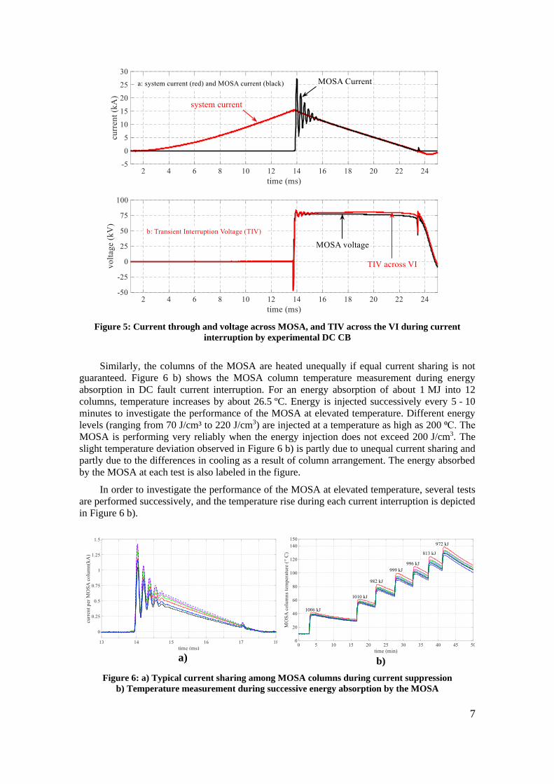
A typical test result of a current interruption by the HVDC circuit breaker is shown in Figure
5. Two MOSA modules, connected in series, are used to double the voltage rating since two
vacuum interrupters are also connected in series. The electrical stresses, namely current and
voltage, of the 12 column MOSA are shown in the figure. The black trace in the top figure shows
the current through the MOSA. The transient overshoots observed are due to the interaction of
the charged capacitor of the breaker and stray inductance in the MOSA circuit. From the bottom
trace in the figure it can be seen that the MOSA maintains the TIV of about 77 kV during the
system current suppression. Unlike in a conventional AC application, where the MOSA conduct
impulse currents for short duration (less than a millisecond), it can be seen from Figure 5 that the
MOSA in HVDC circuit breaker conducts current for about 9.5 ms. Thus, during this period, the
current must be equally distributed throughout the cross-sectional surface of the varistors in order
to avoid local overheating, which could lead to failure. Note that the TIV across the vacuum
interrupter is slightly higher than the voltage across MOSA due to some stray inductance in the
loop. To avoid this difference, the DC CB must be compact designed compact. For the case shown
in Figure 5 about 5.3 MJ energy is dissipated in the two series connected MOSA modules. This
resulted in a temperature rise of about 72 ⁰C. Note that the voltage across the MOSA is more or
less constant even though the system current (through the MOSA) is reducing. This is due to the
fact that, at the beginning of the current suppression, the capacitor (CC) of the breaker is charged
to the same voltage as the MOSA voltage and remain charged during the rest of current
suppression period. When the MOSA voltage tends to reduce following the reduction in the
system current, the capacitor slightly discharges into the MOSA through LC. However, this
discharge is minimal since the voltage difference between the two is also very small. Thus, it does
not affect the voltage across the capacitor.
Figure 6 a) shows a typical current distribution among the MOSA columns measured during
energy absorption. Even if great care is taken during the column matching procedure it is very
difficult to ensure equal current sharing. The matching criterion in this case is, for example, ± 3 %
current deviation from a reference column. It can be seen that the column with the least current
conducts 68 % of the current in the highest conducting column , see the black trace and the dashed
blue trace in Figure 6 a).
7
Figure 5: Current through and voltage across MOSA, and TIV across the VI during current
interruption by experimental DC CB
Similarly, the columns of the MOSA are heated unequally if equal current sharing is not
guaranteed. Figure 6 b) shows the MOSA column temperature measurement during energy
absorption in DC fault current interruption. For an energy absorption of about 1 MJ into 12
columns, temperature increases by about 26.5 ºC. Energy is injected successively every 5 - 10
minutes to investigate the performance of the MOSA at elevated temperature. Different energy
levels (ranging from 70 J/cm³ to 220 J/cm3) are injected at a temperature as high as 200 ⁰C. The
MOSA is performing very reliably when the energy injection does not exceed 200 J/cm3. The
slight temperature deviation observed in Figure 6 b) is partly due to unequal current sharing and
partly due to the differences in cooling as a result of column arrangement. The energy absorbed
by the MOSA at each test is also labeled in the figure.
In order to investigate the performance of the MOSA at elevated temperature, several tests
are performed successively, and the temperature rise during each current interruption is depicted
in Figure 6 b).
a)
b)
Figure 6: a) Typical current sharing among MOSA columns during current suppression
b) Temperature measurement during successive energy absorption by the MOSA

8
Figure 7 a) and b) show thermal images of MOSAs after energy absorption. Part a) shows
the thermal image after successive energy absorption to the model MOSA arrangement. Part b)
shows, as an example of a MOSA of higher voltage rating, the impact of typical unequal current
sharing among the columns and thereby unequal heating of the columns. This is a MOSA in a
different project included here just for comparison. In Figure 6 b) it can be seen that one of the
columns is drawing more current than the other ones and, as a result, heats up to higher values.
This is an observation at much lower energy absorption. This effect could cause a failure if a
nominal energy higher than 200 J/cm3 is rated and that energy is injected.
a) b)
Figure 7: a) Thermal image of MOSA after successive energy absorption b) Impact of unequal
energy sharing – resulting in unequal heating of MOSA columns
V. Aging Phenomena of MOSAs in DC Circuit Breakers
Aging phenomena of MOSAs in AC grids are nowadays well understood [4]. Experienced
manufacturers know how to control the parameters of their makes to change the properties of their
MOSA characteristics. However, in a HVDC CB the requirements and the stresses on the MOSA
are different, as described in the previous section. The main task of the MOSA in a HVDC CB is
the energy absorption during current interruption process.
When the DC CB is in the on-state, the MOSA is short-circuited by the main current path
(the VI), see Figure 1. This allows the MOSA to depolarize, and there is no leakage current under
normal condition [6]. After the DC CB turns into off-state the MOSA is exposed to an impulse
with a fast rise time and a long time to half value (the impulse values will be discussed later). In
general, a DC CB should be operated in series with disconnecting switches. But during the time
period of the DC CB operation up to the opening of the disconnecting switch, the MOSA must
withstand a DC voltage.
A) Aging: Test Setup and Test Cycle
In order to systematically investigate aging phenomena of MOSA in DC circuit breaker
applications, an endurance test circuit for testing individual metal oxide varistors (MOV) is set
up as shown in Figure 8. For this purpose, the test samples are stressed by up to 15 000 impulses,
and a DC voltage is applied for short time directly after impulse injection. The test circuit is
designed to fulfill the requirement of the current impulse described above. The equivalent circuit
of the test setup can be seen in Figure 8, where,
the switch S2 is for depolarization of the MOV;

9
the capacitor C, the resistor R, the inductance L and the switch S1 are generating the
impulse;
the DC source and the switch S3 are generating a DC stress after the impulse current.
The initial switch positions are: S1 open, S2 closed and S3 open. During the charging time
of C the switch S2 is closed. So the MOSA can depolarize for approximately 60 s. After the
capacitor is fully charged switch S2 opens and switch S1 is closed. This generates the desired
impulse for the MOV. The impulse parameters are determined by R, L and the MOV itself. After
the impulse, S1 opens and S2 remains open. S3 is closed, and the MOV is subjected to the DC
stress from the DC source for 2 s. After opening S3 the test cycle starts again.
During the whole cycle, the capacitor voltage and the MOV temperature are constantly
monitored. Impulse current and voltage are measured with an oscilloscope. The oscilloscope data
is transferred to LabVIEW for further calculations and test stand control.
Figure 8: Equivalent circuit of the endurance test stand for combined impulse current and direct
voltage stress
The charging voltage of the capacitor C and the residual voltage of the MOV determine the
amount of energy injected into the MOV. The values of R, L and the characteristics of the MOV
itself determine the rise time and the time to half value.
The test samples are exposed to open air, and their temperature is kept below the limit of
65 °C due to the critical value of 75 °C mentioned in [8]. Recapped, below 75 °C it is ensured
that the MOV only ages electrically. At temperatures above 75 °C there might also be thermal
aging processes in the MOV.
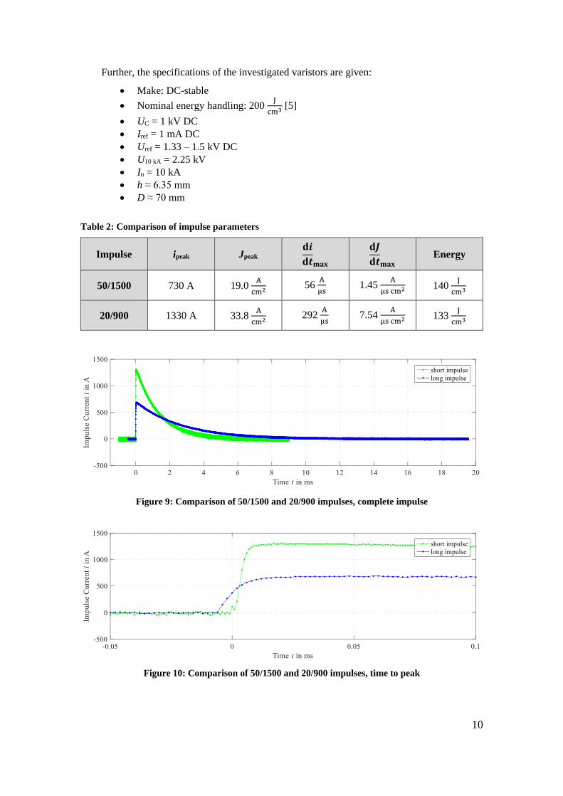
The endurance test stand is able to produce two types of high current impulses. The first
investigations were performed with 50/1500 impulses. This impulse shape represents the
parameters and the stress of a MOSA determined in this project in consultation with an industrial
project partner and based on the investigation of [3]. Important parameters for the impulse are the
values of the RLC circuit in the commutation path, the MOSAs residual voltage in comparison to
the system voltage and the conduction mechanism of the MOSA.
After testing eight MOV samples the impulse shape was changed to a 20/900 impulse. Due
to its higher current rate-of-rise and higher amplitude it imposes more severe stress to the MOV
in terms of electrical aging. While the rise time was decreased from 50 µs to 20 µs and the time
to half value from 1500 µs to 900 µs, the current peak values are increased from 730 A to 1330 A.
A comparison of the two impulses can be seen in Figure 9 and Figure 10, in blue the 50/1500
impulse and in green the 20/900 impulse. Table 2 shows the parameters of the impulses in more
common terms.
Due to experimental restrictions of the endurance test stand, the energy stored in the
capacitor C should not be too high, and specimens with small dimensions (small volume) have to
be used. The specimens for this test series are manufactured out of the same DC stable make as
the larger MOVs used in chapter III and IV.
C
R L S1
V
A
S3
S2 DCMOSA+
-
10
Further, the specifications of the investigated varistors are given:
Make: DC-stable
Nominal energy handling: 200 J
cm3 [5]
UC = 1 kV DC
Iref = 1 mA DC
Uref = 1.33 – 1.5 kV DC
U10 kA = 2.25 kV
In = 10 kA
h ≈ 6.35 mm
D ≈ 70 mm
Table 2: Comparison of impulse parameters
Impulse ipeak Jpeak 𝐝𝒊
𝐝𝒕𝐦𝐚𝐱
𝐝𝑱
𝐝𝒕𝐦𝐚𝐱 Energy
50/1500 730 A 19.0 A
cm2 56 A
μs 1.45
A
μs cm2 140 J
cm3
20/900 1330 A 33.8 A
cm2 292 A
μs 7.54
A
μs cm2 133 J
cm3
Figure 9: Comparison of 50/1500 and 20/900 impulses, complete impulse
Figure 10: Comparison of 50/1500 and 20/900 impulses, time to peak

11
B) Endurance Test Procedure
The endurance test procedure requires interruptions for intermediate electrical
characterization of the MOV. The overall test procedure of one MOV is performed as follows:
Electrical characterization of the new MOV
5000 Impulses
Electrical characterization after 5000 impulses
5000 Impulses
Electrical characterization after 10000 impulses
5000 Impulses
Electrical characterization after 15000 impulses
Determination of the failure energy (destructive test)
Procedure completed
The characterization of the MOV is performed for two regions of its voltage-current-
characteristic, the leakage current region and the protection level current region [4] [8] [9]. The
leakage current region is measured with an automated DC test stand. Because of the small DC
voltage applied to the MOSA and the small current magnitudes, the leakage current measurements
are performed at 35 °C to eliminate any effects of temperature. The current ranges from 10 nA up
to 10 mA. The applied voltage steps are pre-determined in preceding investigations on dummy
MOVs. For high repeatability the recording of the current measurement is started automatically
with a delay of 10 s after the voltage is applied. Due to the extremely low measurement amplitudes
the test stand is monitored with a reference MOV. The reference MOV serves only for monitoring
the DC test stand, no other stress is applied. No changes in the reference MOV characterization
measurements could be observed over the full test time. It can thus be stated that the DC test stand
produces reproducible results and has no impact on possible aging phenomena.
The characterization in the protection level region is measured with a double exponential
current impulse generator. The used impulse is the 8/20 µs [8] [9]. The measurements are taken
at room temperature. The residual voltage is measured at 2.5 kA, 5 kA and 10 kA peak current.
In addition, the voltage-current-characteristic in the current range between 150 A and 750 A
is investigated using the 50/1500 impulse.
C) Evaluation of measured data
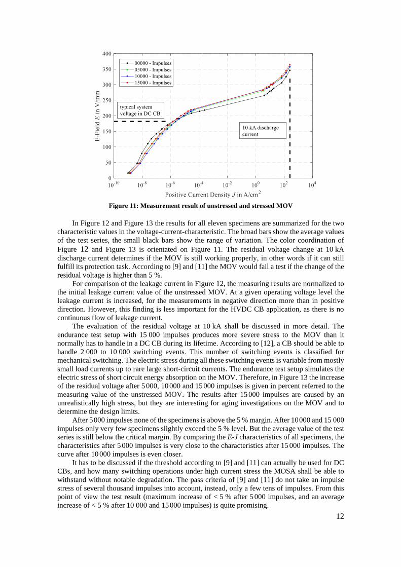
In Figure 11 the typical electric field - current density (E-J) characteristic of one of the
MOVs during the aging process is shown for different numbers of impulse applications. The
characterization is always performed in positive and negative current flow directions through the
MOV. However, in the figure only the positive direction is shown.
In the leakage current region aging phenomena of the MOV can clearly be seen. The new
and aged characteristics are crossing each other at certain point, i.e. they are rotated
counterclockwise around a center at approx. 188 V/mm by the impulse stress. This crossing is
representative of the used make of the MOVs. Similar results were reported e.g. in [10]. This
behavior can usually be accepted as the MOSAs in a HVDC CB application are not continuously
stressed by an applied voltage, and leakage current is typically not an issue.
In the protection level region, aging of the MOV can be observed as well. Aging results in
an increase of the protection level, in this case by approx. 5.5 % as a maximum after 15 000
impulses. This is slightly above the 5 % increase that is in general tolerated according to the IEC
arrester standards [9] [11].
12
Figure 11: Measurement result of unstressed and stressed MOV
In Figure 12 and Figure 13 the results for all eleven specimens are summarized for the two
characteristic values in the voltage-current-characteristic. The broad bars show the average values
of the test series, the small black bars show the range of variation. The color coordination of
Figure 12 and Figure 13 is orientated on Figure 11. The residual voltage change at 10 kA
discharge current determines if the MOV is still working properly, in other words if it can still
fulfill its protection task. According to [9] and [11] the MOV would fail a test if the change of the
residual voltage is higher than 5 %.
For comparison of the leakage current in Figure 12, the measuring results are normalized to
the initial leakage current value of the unstressed MOV. At a given operating voltage level the
leakage current is increased, for the measurements in negative direction more than in positive
direction. However, this finding is less important for the HVDC CB application, as there is no
continuous flow of leakage current.
The evaluation of the residual voltage at 10 kA shall be discussed in more detail. The
endurance test setup with 15 000 impulses produces more severe stress to the MOV than it
normally has to handle in a DC CB during its lifetime. According to [12], a CB should be able to
handle 2 000 to 10 000 switching events. This number of switching events is classified for
mechanical switching. The electric stress during all these switching events is variable from mostly
small load currents up to rare large short-circuit currents. The endurance test setup simulates the
electric stress of short circuit energy absorption on the MOV. Therefore, in Figure 13 the increase
of the residual voltage after 5 000, 10 000 and 15 000 impulses is given in percent referred to the
measuring value of the unstressed MOV. The results after 15 000 impulses are caused by an
unrealistically high stress, but they are interesting for aging investigations on the MOV and to
determine the design limits.
After 5 000 impulses none of the specimens is above the 5 % margin. After 10 000 and 15 000
impulses only very few specimens slightly exceed the 5 % level. But the average value of the test
series is still below the critical margin. By comparing the E-J characteristics of all specimens, the
characteristics after 5 000 impulses is very close to the characteristics after 15 000 impulses. The
curve after 10 000 impulses is even closer.
It has to be discussed if the threshold according to [9] and [11] can actually be used for DC
CBs, and how many switching operations under high current stress the MOSA shall be able to
withstand without notable degradation. The pass criteria of [9] and [11] do not take an impulse
stress of several thousand impulses into account, instead, only a few tens of impulses. From this
point of view the test result (maximum increase of < 5 % after 5 000 impulses, and an average
increase of < 5 % after 10 000 and 15 000 impulses) is quite promising.

13
The TIV during a load current and a short-circuit current switching event reaches the same
amplitude. But due to the larger magnetic energy of the shirt-circuit event the MOSA has to deal
with much higher energy absorption (e.g. its full rated energy handling capability). If this high
energy absorption happens less than 5 000 times during the lifespan of a DC CB, all MOVs are
within the so far tolerated clamping voltage increase. Switching such high currents for 5 000 times
in a DC grid seems to be very unrealistic, however.
The main task of the MOSA in the DC CB is not to limit to a certain voltage, and the slight
increase of the residual voltage in the DC CB should not be critical. Its main task is to absorb
large amounts of energy. And as shown in Table 3 the energy absorption capability is getting even
better after impulse current stress.
a)
b)
Figure 12: Normalized changes of the leakage current at typical system voltage in DC CB after
5000, 10000 and 15000 impulses, a) positive current direction, b) negative current direction
a)
b)
Figure 13: Changes of the residual voltage after 5000, 10000 and 15000 impulses, a) positive current
direction, b) negative current direction
By comparing each individual change in leakage current, residual voltage and
characterization curves between the 50/15000 and the 20/900 impulse, the 20/900 should be more
critical for the MOV. But the results show that specimen stressed with the 20/900 impulse behave
like all others and there is no significant higher stress for the MOV. This leads to the assumption
that the current rate of rise and the amplitude are manageable from the MOVs. The injected
amount of energy seems to be the main factor for aging.

14
The final investigation on the MOVs is the failure energy test. This test is performed with
alternating current in the range of 200 A peak value, because this is a very effective way to
determine changes in failure energy quickly [5] [8]. The current flows until mechanical damage
of the specimen. The failure energy was measured for twelve unstressed MOVs and the eleven
MOVs stressed in the preceding endurance test procedure. In Table 3 the results of this
investigation are listed.
Table 3: Comparison of failure energies
Unstressed Stressed
Mean failure energy 855.72 J
cm3 899.37 J
cm3
Max. failure energy 995.81 J
cm3 962.70 J
cm3
Min. failure energy 706.63 J
cm3 824.49 J
cm3
Standard deviation 97.70 40.60
Peak current 219.00 A 208.41 A
Current density 5.69 A
cm2 5.42 A
cm2
The mean failure energy of the stressed MOVs is 5.1 % higher in comparison to the
unstressed MOVs. While an actual increase in failure energy seems questionable, it can, however,
be stated that the failure energy is definitely not decreased by the endurance test.
In particular the standard deviation is remarkable. The standard deviation is reduced by a
factor of 0.41. This suggests that the conditioning (by the endurance test) of the MOVs has some
sort of leveling effect. The stressed MOVs’ material might be more homogeneous after the
repeated energy stress. This could be a positive effect for large MOSA banks in DC CBs. High
energy stress might be better distributed between the MOSA columns after several switching
events.
VI. Conclusion
The ongoing research on HVDC CB is crucial for multi-terminal, meshed HVDC grids. The
MOSA is an essential component of a HVDC CB. Most papers are focusing on the fundamental
functionality of the DC CB. Closer investigations on partial components of a DC CB and,
therefore, the dedicated use in DC CB is rare to find. This paper deals with the duties and stresses
of MOSA in HVDC CBs.
The differences of MOSA as a protection unit and in DC CB are discussed. The main task
for the MOSA in a DC CB is to handle the TIV stress and energy consumption during a DC
switching event. For a better understanding of the MOSA stress, a basic introduction into DC
switching using the example of a DC CB with mechanical switching element (VI) and active
commutation path is given [3].
Due to the large amount of energy consumption the MOSA has to deal with, several design
issues with respect to energy handling, current distribution and TIV are discussed. In summary,
the energy handling and the TIV determine the amount of paralleled MOSA columns that have to
be used. But it has to be considered that with more MOSA columns in parallel the TIV slightly
drops.

15
During several HVDC switching tests a large MOSA setup was investigated. The
temperature as well as the current distribution through each column is monitored. Differences in
temperature rise and current distribution are discussed. Also maximum energy and temperature
handling are investigated.
Furthermore the aging of MOVs used in the MOSA is investigated with a customized
endurance test stand. All the stresses in a DC CB are simulated in the test stand. As a result, the
MOSA is expected to withstand the stresses over the lifespan of a CB. The E-J-characteristic is
measured before, during and after the aging process. For comparison of the unstressed and
stressed MOSA, criteria from [8] [9] and [11] are used.
In this project only one MOV make could be investigated. To get more information and for
better statistics on the behavior of MOSA in DC CB more MOV makes should be investigated in
the future.
Acknowledgment
The works on surge arresters in an experimental DC CB in this paper are supported by
funding from European Union’s horizon 2020 research and innovation programme under grant
agreement No. 691714.
References
[1] N. A. Belda and R. P. P. Smeets, "Test Circuits for HVDC Circuit Breakers," IEEE
Transaction on Power Delivery, vol. 32, no. 1, pp. 285 - 293, 2017.
[2] C. M. Franck, "HVDC Circuit Breakers: A Review Identifying Future Research Needs,"
IEEE Transaction on Power Delivery, vol. 26, no. 2, pp. 998 - 1007, 2011.
[3] T. Heinz, Gleichstromschalten in der Mittel- und Hochspannungstechnik unter Einsatz
von Vakuumschaltröhren, Darmstadt, Germany: TU Darmstadt, 2017.
[4] V. Hinrichsen, Metal-Oxide Surge Arresters in High-Voltage Power Systems, Berlin and
Darmstadt: Siemens, 2011.
[5] M. Tuczek, Experimental Investigations of the Multiple Impulse Energy Handling
Capability of Metal-Oxide Varistors for Applications in Electrical Power Engineering,
Darmstadt, Germany: TU Darmstadt, 2015.
[6] W. Bassi and H. Tatizawa, "Early Prediction of Surge Arrester Failures by Dielectric
Characterization," IEEE Electrical Insulation Magazine, vol. 32, no. 2, pp. 35-42, 2016.
[7] N. A. Belda, C. A. Plet and R. P. P. Smeets, "Full-Power Test of HVDC Circuit-Breakers
with AC Short-Circuit Generators Operated at low Power Frequency," IEEE Transactions
on Power Delivery ( Early Access ), pp. 1-1, 2019.
[8] CIGRE TB 544, "MO Surge Arresters - Stresses and Test Procedures," CIGRE, Paris,
2013.
[9] IEC 60099-9, Surge arresters – Part 9: Metal-oxide surge arresters without gaps for
HVDC converter stations, IEC Standards, 2014.
[10] M. Bröker and V. Hinrichsen, "Testing Metal-Oxide Varistors for HVDC Breaker
Application," IEEE Transaction on Power Delivery, vol. 34, no. 1, pp. 346 - 352, 2019.
[11] IEC 60099-4, Surge arresters – Part 4: Metal-oxide surge arresters without gaps for a.c.
systems, IEC standards, 2014.
[12] IEC62271-100, High-voltage switchgear and controlgear – Part 100: Alternating-current
circuit-breakers, IEC Standards, 2008.

16
Authors
Peter Hock received his
M.Sc. in electrical
engineering in 2015 from
Technische Universität
Darmstadt, Germany. Since
2016, he is a research
associate at TU Darmstadt in
the working group of Prof.
Volker Hinrichsen. His main
focus is investigation of
HVDC circuit breakers with special interest on the
metal-oxide surge arrester as an energy absorption
element in the breaker. Other research topics have been
accelerated ageing of composite insulators made from
epoxy resin filled with microvaristor particles as well as
arc interrupting behavior of direct current load switches
in electrified railways. He is active in CIGRE Working
Group A3.40.
Volker Hinrichsen worked
with Siemens from 1989 to
2001, where he held the
position of Director R&D of
the Surge Arrester Division.
Since 2001, he is full
professor in high-voltage
engineering at Technische
Universitat Darmstadt,
Germany. He is a member of
several Committees and Working Groups within IEC,
IEEE, Cigre and VDE/DKE. He is Chairman of IEC
TC37 (Surge Arresters) and Convenor of IEC TC37
MT4, responsible for all high-voltage arrester test
standards. His most recent research activities in the field
of surge arresters have been on energy handling
capability and on optimization of external grading
systems of UHV arresters.
Nadew Belda received a joint
M.Sc. in electric power
engineering from the
Eindhoven University of
Technology (TU/e) and the
Royal Institute of Technology
(KTH), Sweden. Currently,
Mr. Belda is with KEMA
Laboratories, Innovation
Section, responsible for the
development of test methods and design of test circuits
for HVDC switchgear. His research is part of his Ph.D.
at Technische Universität Darmstadt (TU Darmstadt),
Germany, where he is an external Ph.D. candidate. He is
a member of IEEE and CIGRE and actively participates
in related Working Groups.
René Peter Paul Smeets received a Ph.D degree for
research work on switchgear
in 1987. Until 1995, he was
an assistant professor at
Eindhoven University.
During 1991 he worked with
Toshiba Corporation in
Japan. In 1995, he joined
KEMA, the Netherlands. At
present, he is with KEMA Laboratories of DNV GL, as
a service area and innovation leader. In 2001 he was
appointed part-time professor at Eindhoven University,
the Netherlands in the field of high-power switching and
testing technology. In 2013 he became adjunct professor
at Xi’an Jiaotong University, China.
Dr. Smeets is convener/member of working groups and
study/advisory committees of CIGRE in the field of
emerging high-voltage equipment such as high-voltage
vacuum -, HVDC switchgear and SF6 alternatives.
In 2008 he was elected Fellow of IEEE and since 2008
he is chairman of the “Current Zero Club”, a scientific
study committee on current interruption. He received six
international awards, among which two from IEEE. He
is convener of two maintenance teams in IEC on high-
voltage switchgear.
Dr. Smeets published and edited three books and
authored over 300 international papers on testing and
switching in power systems, in addition to many
tutorials all over the world.


![Energy Division LV and MV Metal-Oxide Surge Arresters · Overview of ZnO surge arresters offered by Tyco Electronics Energy Division Type Rating [kA] Line Application Continuous Page](https://static.fdocuments.in/doc/165x107/5f048d217e708231d40e87bb/energy-division-lv-and-mv-metal-oxide-surge-overview-of-zno-surge-arresters-offered.jpg)