Investigation of Electromagnetic Interference of PWM Motor ...
75
Investigation of Electromagnetic Interference of PWM Motor Drives in Automotive Electrical Systems by Feng Zhang Submitted to the Department of Electrical Engineering and Computer Science in partial fulfillment of the requirements for the degree of Master of Science at the MASSACHUSETTS INSTITUTE OF TECHNOLOGY May 1999 @ Massachusetts Institute 5ichnolog1 . All rights reserved. A u th or ............. I........................................................... Department of Electrical Engineering and Computer Science May 18, 1999 // / / /1 1 I9 Certified by... ...... .. ....... .. John G. Kassakian Professor of Electrical Engineering and Computer Science Thesis Supervisor Certified by....... .. . Stephan H. Guttowski Visiting Scientist Thesis Supervisor 7- 7-9~ 7 ------- 9 7-- -y Accepted by ..................... ...-........................ Arthur C. Smith Chairman, Department Committee on Graduate Students
Transcript of Investigation of Electromagnetic Interference of PWM Motor ...
Investigation of Electromagnetic Interference of PWM
Motor Drives in Automotive Electrical Systems
by
Feng Zhang
Submitted to the Department of Electrical Engineering and Computer Sciencein partial fulfillment of the requirements for the degree of
Master of Science
at the
MASSACHUSETTS INSTITUTE OF TECHNOLOGY
May 1999
@ Massachusetts Institute 5ichnolog1 . All rights reserved.
A u th or ............. I...........................................................Department of Electrical Engineering and Computer Science
May 18, 1999
/// /
/11 I9
Certified by... ...... .. ....... ..John G. Kassakian
Professor of Electrical Engineering and Computer ScienceThesis Supervisor
Certified by....... .. .Stephan H. Guttowski
Visiting ScientistThesis Supervisor
7- 7-9~
7
------- 97-- -y
Accepted by ..................... ...-........................
Arthur C. SmithChairman, Department Committee on Graduate Students
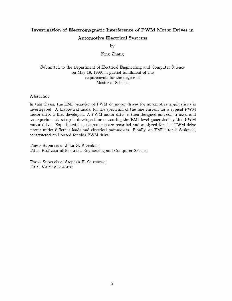
Investigation of Electromagnetic Interference of PWM Motor Drives in
Automotive Electrical Systems
by
Feng Zhang
Submitted to the Department of Electrical Engineering and Computer Scienceon May 18, 1999, in partial fulfillment of the
requirements for the degree ofMaster of Science
Abstract
In this thesis, the EMI behavior of PWM dc motor drives for automotive applications isinvestigated. A theoretical model for the spectrum of the line current for a typical PWMmotor drive is first developed. A PWM motor drive is then designed and constructed andan experimental setup is developed for measuring the EMI level generated by this PWMmotor drive. Experimental measurements are recorded and analyzed for this PWM drivecircuit under different loads and electrical parameters. Finally, an EMI filter is designed,constructed and tested for this PWM drive.
Thesis Supervisor: John G. KassakianTitle: Professor of Electrical Engineering and Computer Science
Thesis Supervisor: Stephan H. GuttowskiTitle: Visiting Scientist
2
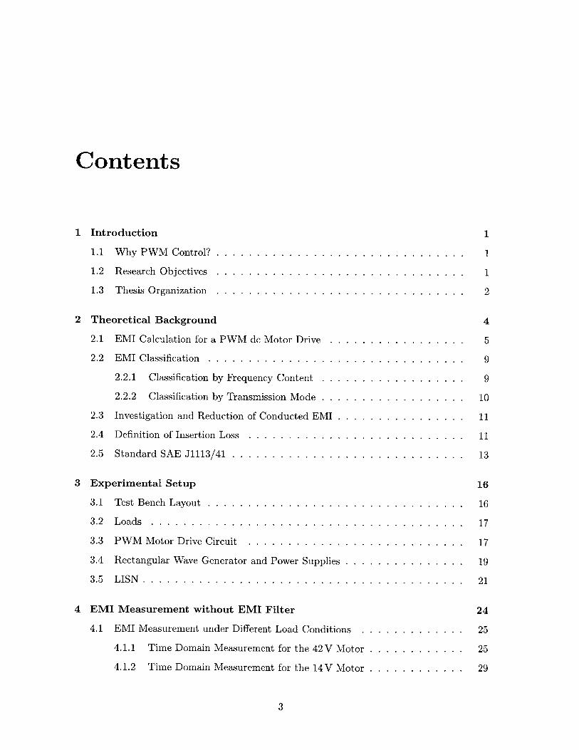
Contents
1 Introduction
1.1 Why PWM Control? ...............
1.2
1.3
Research Objectives ... ...............
Thesis Organization . . . . . . . . . . . . . . .
2 Theoretical Background
2.1 EMI Calculation for a PWM dc Motor Drive . . . . .
2.2 EM I Classification . . . . . . . . . . . . . . . . . . . .
2.2.1 Classification by Frequency Content . . . . . .
2.2.2 Classification by Transmission Mode . . . . . .
2.3 Investigation and Reduction of Conducted EMI . . . .
2.4 Definition of Insertion Loss . . . . . . . . . . . . . . .
2.5 Standard SAE J1113/41 . . . . . . . . . . . . . . . . .
3 Experimental Setup
3.1 Test Bench Layout . . . . . . . . . . . . . . . . . . . .
3.2 Loads . . . . . . . . . . . . . . . . . . . . . . . . . . .
3.3 PWM Motor Drive Circuit . . . . . . . . . . . . . . .
3.4 Rectangular Wave Generator and Power Supplies . . .
3.5 LISN . . . . . . . . . . . . . . . . . . . . . . . . . . . .
4 EMI Measurement without EMI Filter
4.1 EMI Measurement under Different Load Conditions
4.1.1 Time Domain Measurement for the 42 V Motor
4.1.2 Time Domain Measurement for the 14V Motor
3
1
. .. . 1
. .. . .. .. .. 1
. . . . . . . . . . 2
4
5
9
9
10
11
11
13
16
. . . . . . . . . . 16
. . . . . . . . . . 17
. . . . . . . . . . 17
. . . . . . . . . . 19
. . . . . . . . . . 21
24
25
25
29
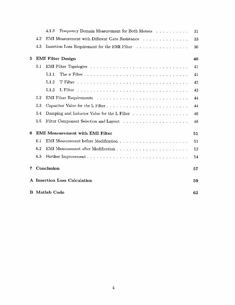
4.1.3 Frequency Domain Measurement for Both Motors . . . . . .
4.2 EMI Measurement with Different Gate Resistance . . . . . . . . . .
4.3 Insertion Loss Requirement for the EMI Filter . . . . . . . . . . . .
. . . 31
. . . 33
. . . 36
5 EMI Filter Design
5.1 EMI Filter Topologies . . . . . . . . . . . . .
5.1.1 The 7r Filter . . . . . . . . . . . . . . .
5.1.2 T Filter . . . . . . . . . . . . . . . . .
5.1.3 L Filter . . . . . . . . . . . . . . . . .
5.2 EMI Filter Requirements . . . . . . . . . . .
5.3 Capacitor Value for the L Filter . . . . . . . .
5.4 Damping and Inductor Value for the L Filter
5.5 Filter Component Selection and Layout . . .
6 EMI Measurement with EMI Filter
6.1 EMI Measurement before Modification . . . . . . . . . . . . . . . . . . . . .
6.2 EMI Measurement after Modification . . . . . . . . . . . . . . . . . . . . . .
6.3 Further Improvement . . . . . . . . . . . . . . . . . . . . . . . . . . . . . . .
7 Conclusion
A Insertion Loss Calculation
B Matlab Code
4
40
. . . . . . . . . . . . . . . . . 4 1
. . . . . . . . . . . . . . . . . 4 1
. . . . . . . . . . . . . . . . . 42
. . . . . . . . . . . . . . . . . 43
. . . . . . . . . . . . . . . . . 44
. . . . . . . . . . . . . . . . . 44
. . . . . . . . . . . . . . . . . 46
. . . . . . . . . . . . . . . . . 48
51
51
52
54
57
59
62
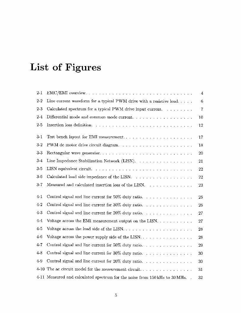
List of Figures
2-1 EMC/EMI overview. . . . . . . . . . . . . . . . . . . . . . . . . . . . .
2-2 Line current waveform for a typical PWM drive with a resistive load. .
2-3 Calculated spectrum for a typical PWM drive input current. . . . . .
2-4 Differential mode and common mode current. . . . . . . . . . . . . . .
2-5 Insertion loss definition. . . . . . . . . . . . . . . . . . . . . . . . . . .
3-1 Test bench layout for EMI measurement .. . . . . . . . . . . . . . . . .
3-2 PWM dc motor drive circuit diagram. . . . . . . . . . . . . . . . . . .
3-3 Rectangular wave generator. . . . . . . . . . . . . . . . . . . . . . . . .
3-4 Line Impedance Stabilization Network (LISN). . . . . . . . . . . . . .
3-5 LISN equivalent circuit. . . . . . . . . . . . . . . . . . . . . . . . . . .
3-6 Calculated load side impedance of the LISN. . . . . . . . . . . . . . .
3-7 Measured and calculated insertion loss of the LISN. . . . . . . . . . .
4-1
4-2
4-3
4-4
4-5
4-6
4-7
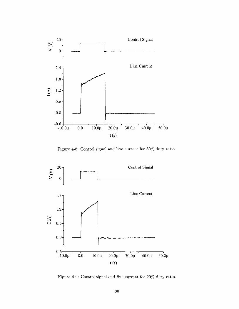
4-8
4-9
4-10
Control signal and line current for 50% duty ratio. . . . . .
Control signal and line current for 30% duty ratio. . . . . .
Control signal and line current for 20% duty ratio. . . . . .
Voltage across the EMI measurement output on the LISN. .
Voltage across the load side of the LISN. . . . . . . . . . . .
Voltage across the power supply side of the LISN . . . . . .
Control signal and line current for 50% duty ratio. . . . . .
Control signal and line current for 30% duty ratio. . . . . .
Control signal and line current for 20% duty ratio. . . . . .
The ac circuit model for the measurement circuit. . . . . . .
4-11 Measured and calculated spectrum for the noise from 150 kHz to 30 MHz.
5
4
6
7
10
12
17
18
20
21
22
22
23
. . . . . . 26
. . . . . . 26
. . . . . . 27
. . . . . . 27
. . . . . . 28
. . . . . . 28
. . . . . . 29
. . . . . . 30
. . . . . . 30
. . . . . . 31
32
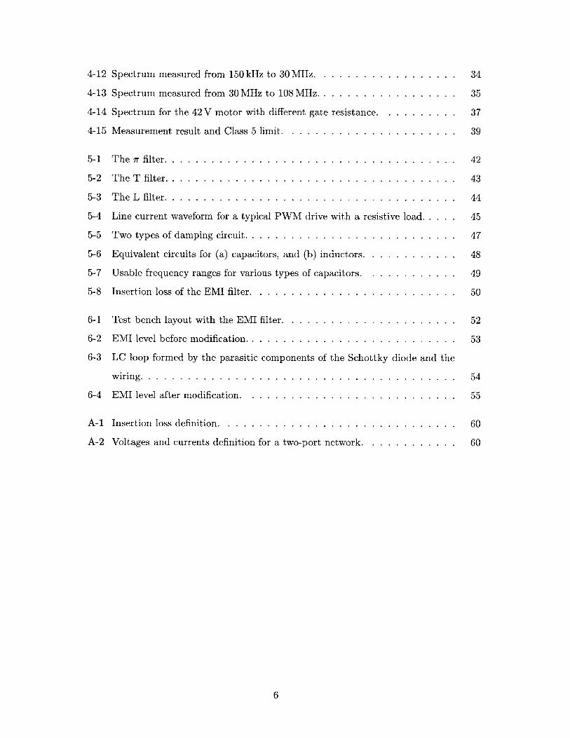
4-12 Spectrum measured from 150 kHz to 30 MHz. . . . . . . . . . . . . . . . . . 34
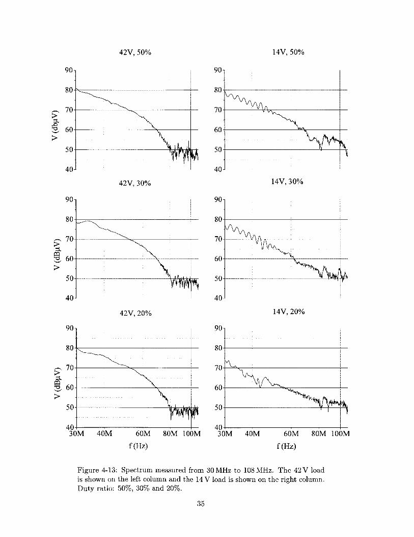
4-13 Spectrum measured from 30 MHz to 108 MHz. . . . . . . . . . . . . . . . . . 35
4-14 Spectrum for the 42 V motor with different gate resistance. . . . . . . . . . 37
4-15 Measurement result and Class 5 limit. . . . . . . . . . . . . . . . . . . . . . 39
5-1 T he 7r filter. . . . . . . . . . . . . . . . . . . . . . . . . . . . . . . . . . . . . 42
5-2 The T filter. . . . . . . . . . . . . . . . . . . . . . . . . . . . . . . . . . . . . 43
5-3 The L filter. . . . . . . . . . . . . . . . . . . . . . . . . . . . . . . . . . . . . 44
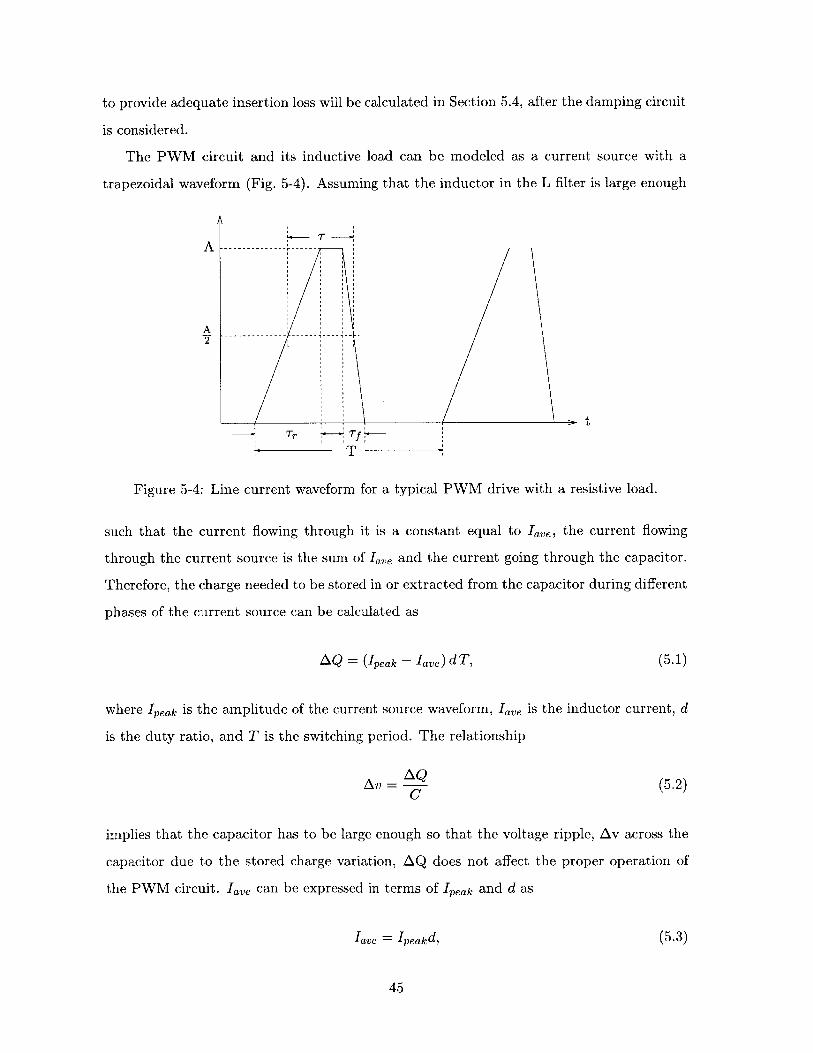
5-4 Line current waveform for a typical PWM drive with a resistive load. . . . . 45
5-5 Two types of damping circuit. . . . . . . . . . . . . . . . . . . . . . . . . . . 47
5-6 Equivalent circuits for (a) capacitors, and (b) inductors. . . . . . . . . . . . 48
5-7 Usable frequency ranges for various types of capacitors. . . . . . . . . . . . 49
5-8 Insertion loss of the EMI filter. . . . . . . . . . . . . . . . . . . . . . . . . . 50
6-1 Test bench layout with the EMI filter. . . . . . . . . . . . . . . . . . . . . . 52
6-2 EMI level before modification. . . . . . . . . . . . . . . . . . . . . . . . . . . 53
6-3 LC loop formed by the parasitic components of the Schottky diode and the
w iring. . . . . . . . . . . . . . . . . . . . . . . . . . . . . . . . . . . . . . . . 54
6-4 EMI level after modification. . . . . . . . . . . . . . . . . . . . . . . . . . . 55
A-1 Insertion loss definition. . . . . . . . . . . . . . . . . . . . . . . . . . . . . . 60
A-2 Voltages and currents definition for a two-port network. . . . . . . . . . . . 60
6
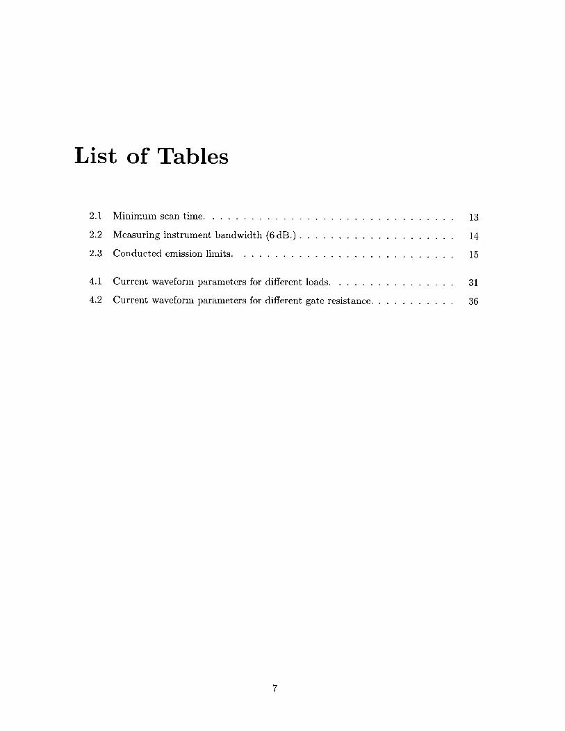
List of Tables
2.1 M inimum scan time. ................................ 13
2.2 Measuring instrument bandwidth (6 dB.) . . . . . . . . . . . . . . . . . . . . 14
2.3 Conducted emission limits. . . . . . . . . . . . . . . . . . . . . . . . . . . . 15
4.1 Current waveform parameters for different loads. . . . . . . . . . . . . . . . 31
4.2 Current waveform parameters for different gate resistance. . . . . . . . . . . 36
7
Chapter 1
Introduction
1.1 Why PWM Control?
To make driving a safer, more comfortable, and more exciting experience, automobile de-
signers keep including electronic devices into their designs, which require higher power from
the power supply. Increased awareness of environmental issues has resulted in demands for
substantial improvements in fuel efficiency in today's automobiles. These demands become
a great challenge in future automobile designs. The current 14V system, however, has a
very difficult time meeting this challenge economically. A solution to this problem is a new
14 V/42 V dual-voltage system [1].
With a 42 V power supply available, alternative ways of operating existing devices,
e.g., various dc motors and lamps, can greatly improve the performance of such devices.
One appealing example is to use pulse-width modulated (PWM) control to manipulate the
operation of the motors and lamps. Not only does PWM control improve the controllability
and efficiency of such devices, but it also allows automobile designers to easily accommodate
new features in their design, e.g., varying the speed of dc motors or adjusting the brightness
of lamps. Power MOSFETs are ideal for such applications, and they are more economical
at 42 V than at 14 V in many aspects.
1.2 Research Objectives
While semiconductor based PWM motor drives bring many advantages, they introduce
electrical noise to the surrounding environment which can cause operational failures of other
1
electronic devices, e.g., ECUs and radio receivers [2]. Usually an EMI filter is required to
suppress this unwanted noise. A good understanding of the electrical characteristics of
the PWM motor drives, especially their electromagnetic interference (EMI) behavior, can
significantly reduce the cost of EMI filter design [3]. In the mean time, no standard exists
for the 42V electrical system, and what levels of conducted emission should be expected
from such a system are not very clear. Therefore, some accurate EMI measurements on the
PWM motor drives and a thorough analysis of these measurement results are invaluable for
both the EMI designers and those who establish the standard.
The objectives of this research project are to:
1. Predict the EMI behavior of a typical PWM dc motor drive used in automotive
applications through theoretical calculations;
2. Conduct a series of EMI measurements with a prototype PWM dc motor drive under
various load conditions and electrical parameters;
3. Analyze the measurement results and comparing them with the theoretical calcula-
tions;
4. Develop a simple and effective EMI filter design methodology for this particular ap-
plication.
1.3 Thesis Organization
The project is divided into several different stages, and the thesis is organized in chapters
accordingly. The content of each chapter is described briefly below.
The second chapter conducts a theoretical calculation for the noise emission of PWM
motor drives. It also defines EMI/EMC and provides some background knowledge of
EMI/EMC classification and EMI standards adopted by the automotive industry.
The third chapter describes a measurement test setup specified by the EMI standard,
and describes each functional unit in the setup. Schematics of important functional units,
such as the prototype PWM motor drive and the Line Impedance Stabilization Network
(LISN) are shown.
The fourth chapter presents EMI measurement results for a prototype PWM dc motor
drive under various load conditions and electrical parameters along with a detailed analysis
2
of these results. The measurement is conducted without any filter element in the circuit.
The measured EMI level is then compared to the existing standard, and the insertion loss
required to meet the standard is calculated.
The fifth chapter describes several most common EMI filter topologies and their advan-
tages and disadvantages. constraints on EMI filter design for this particular application are
listed. A simple and reliable EMI filter design method will be presented.
The sixth chapter presents EMI measurement results with the EMI filter inserted into the
system. Necessary modifications for improving the performance of the filter are discussed.
The last chapter presents conclusions and recommendations for future work.
3
Chapter 2
Theoretical Background
Electromagnetic Interference (EMI) is a problem that exists in all electrical systems. All
electrical circuits emit electrical noise while operating. If not controlled properly, the noise
can affect the normal operation of other devices, or even destroy them, through common
electrical connections or electromagnetic coupling. The issue of compatibility among electri-
cal devices in a system or common environment has evolved into an engineering discipline,
Electromagnetic Compatibility, or EMC. EMC is an engineering discipline that investigates
the amount of electrical noise that different devices can generate or tolerate, and estab-
lishes standards to provide limits on the amount of noise different devices should generate
or be able to tolerate, in order to have them work together in a system or a common
environment [21.
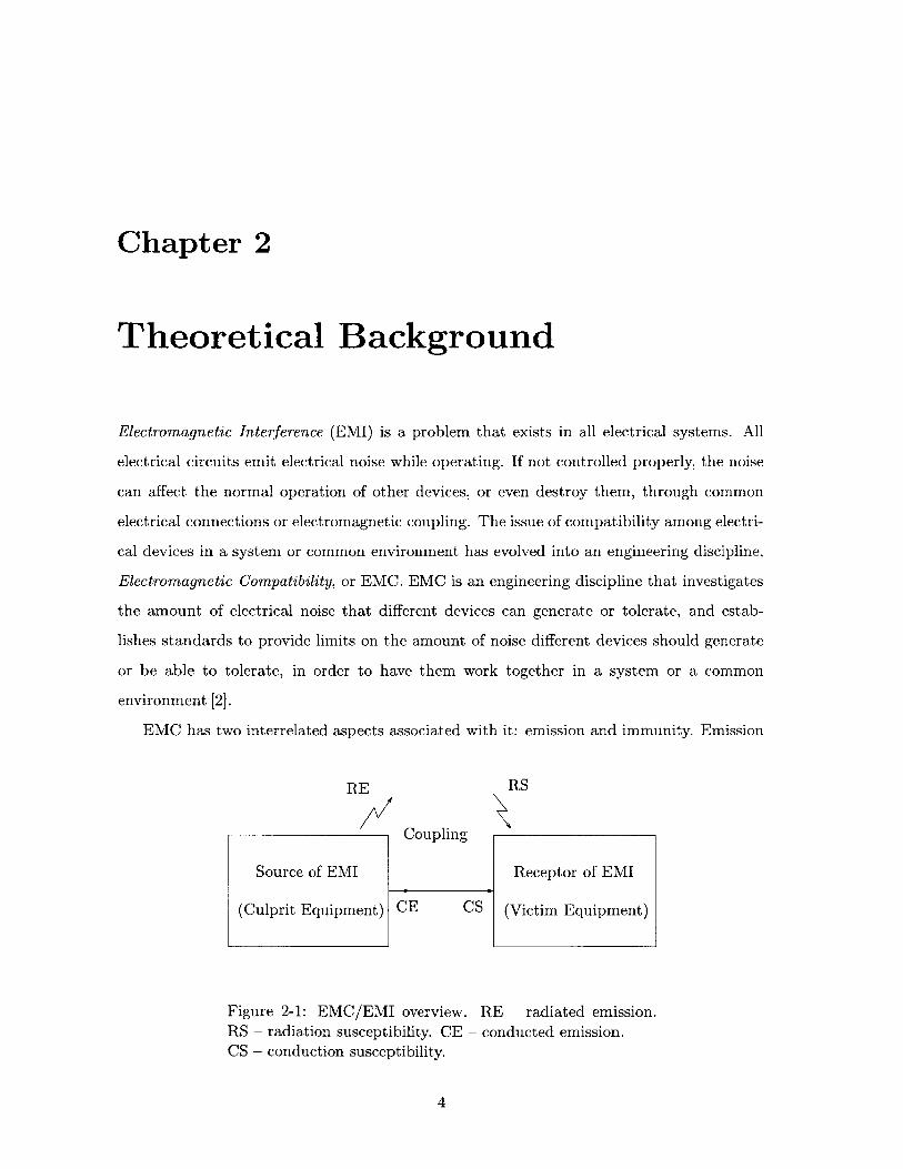
EMC has two interrelated aspects associated with it: emission and immunity. Emission
RE RS
Coupling
Source of EMI Receptor of EMI
(Culprit Equipment) CE CS (Victim Equipment)
Figure 2-1: EMC/EMI overview. RE - radiated emission.RS - radiation susceptibility. CE - conducted emission.CS - conduction susceptibility.
4
deals with how much noise emitted by each of the devices in a common environment should
be allowed such that the total noise existing in the environment is not fatal for the normal
operation of any individual device. Immunity is concerned with how much noise a device
should be able to withstand before it malfunctions.
In this chapter, characteristics of the noise generated by a PWM drive circuit will be
examined and basic background knowledge of EMI will be provided.
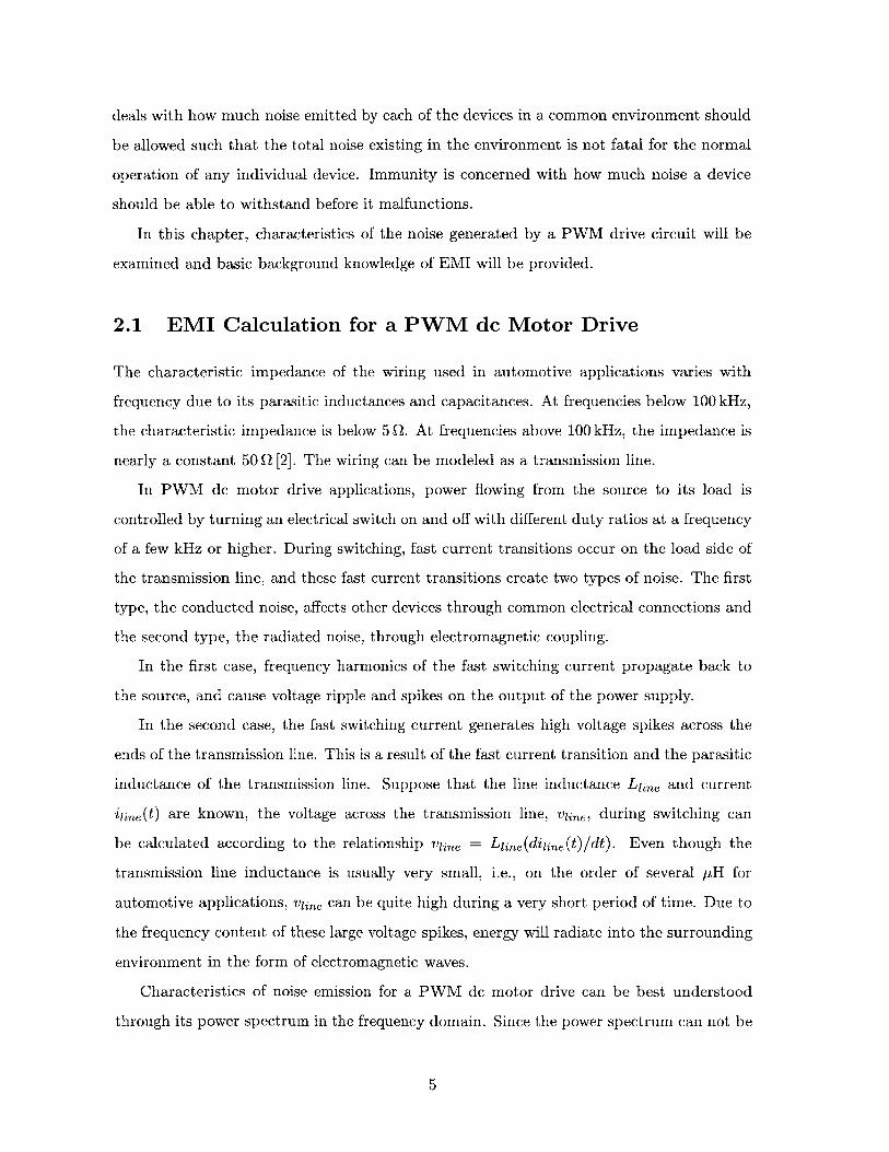
2.1 EMI Calculation for a PWM dc Motor Drive
The characteristic impedance of the wiring used in automotive applications varies with
frequency due to its parasitic inductances and capacitances. At frequencies below 100 kHz,
the characteristic impedance is below 5 Q. At frequencies above 100 kHz, the impedance is
nearly a constant 50 Q [2]. The wiring can be modeled as a transmission line.
In PWM dc motor drive applications, power flowing from the source to its load is
controlled by turning an electrical switch on and off with different duty ratios at a frequency
of a few kHz or higher. During switching, fast current transitions occur on the load side of
the transmission line, and these fast current transitions create two types of noise. The first
type, the conducted noise, affects other devices through common electrical connections and
the second type, the radiated noise, through electromagnetic coupling.
In the first case, frequency harmonics of the fast switching current propagate back to
the source, and cause voltage ripple and spikes on the output of the power supply.
In the second case, the fast switching current generates high voltage spikes across the
ends of the transmission line. This is a result of the fast current transition and the parasitic
inductance of the transmission line. Suppose that the line inductance Lline and current
'iine(t) are known, the voltage across the transmission line, vline, during switching can
be calculated according to the relationship Vline = Liine(diiine(t)/dt). Even though the
transmission line inductance is usually very small, i.e., on the order of several PH for
automotive applications, Viine can be quite high during a very short period of time. Due to
the frequency content of these large voltage spikes, energy will radiate into the surrounding
environment in the form of electromagnetic waves.
Characteristics of noise emission for a PWM dc motor drive can be best understood
through its power spectrum in the frequency domain. Since the power spectrum can not be
5
measured directly, the voltage spectrum is usually used instead. The power spectrum can
then be deduced from the voltage spectrum.
Figure 2-2 approximates the line current waveform of a PWM motor drive circuit with
resistive or highly inductive loads. A is the amplitude of the waveform. T is the period, R,
l\-
A-------- ------
A-
t~~ITrT
Figure 2-2: Line current waveform for a typical PWM drive with a resistive load.
F, and d are the relative rise time, the relative fall time and the duty ratio, respectively.
The variables R, F, d are related to T by the following expressions:
R = rr/T, relative rise time,
F = rf/T, relative fall time,
d = r/T, duty ratio, (2.1)
with the constraintsR+F R+F
d + <1 and ( d. (2.2)2 2
Since the duty ratio varies much slower in time than the switching frequency, it is assumed
to be a constant in the calculation.
The spectrum of this current waveform can be derived through Fourier analysis [4].
Since the current waveform is periodic, its spectrum has nonzero values only at discrete
frequencies, e.g., dc, the switching frequency and its higher harmonics. The harmonics for
the switching frequency can be expressed in terms of the harmonic number, k, as fk = kf,
where f,, is the switching frequency, and fk is its kth harmonic. Given the time domain
6

signal is s(t), its Fourier transform, expressed in terms of k, is
S(k) = A ( sinc (7rkR) e js'kd7rk
- sinc (irkF) e-jTkd),
where sinc (x) = sin (x)/x.
The amplitude spectrum of the waveform shown in Fig. 2-2 is plotted in Fig. 2-3 for the
following set of parameters: A = 1/v/Z A, R =.008, F =.01, d =.2, and fs, =20 kHz. The
envelope shown in the figure, described in the next paragraph, tracks the local maxima of
the waveform tightly. Frequency spectrum analysis shows that the energy level of the noise
120
100
80
60
40
20
0100k iM 10M
frequency (Hz)
Figure 2-3: Calculated spectrum for a typical PWM driveinput current.
concentrates at the switching frequency and its low harmonics. The energy level decreases
rapidly as frequency increases [4]. Other parameters, such as duty ratio, rise time and fall
time, determine the shape of the envelope.
The envelope of the spectrum can be divided into four segments. For low frequencies,
i.e., between the switching frequency and the first cutoff harmonic, the segment is a constant
7
(2.3)
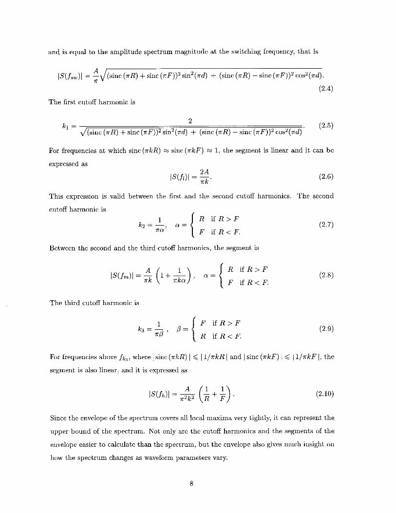
and is equal to the amplitude spectrum magnitude at the switching frequency, that is
IS(f8W)| = - (sinc (irR) + sinc (irF))2 sin2 (7rd) + (sinc (7rR) - sinc (rF))2 cos 2 (ird).
(2.4)
The first cutoff harmonic is
2ki = V/sn -r)+sn iF) i2 2(2.5)
v/(sinc (irR) + sinc (irF))2 sin2 (7rd) + (sinc (irR) - sinc (7rF))2 cos 2 (7rd)
For frequencies at which sinc (7rkR) ~ sinc (7rkF) ~ 1, the segment is linear and it can be
expressed as
IS(fi)= 2A (2.6)irk
This expression is valid between the first and the second cutoff harmonics. The second
cutoff harmonic is
1 R ifR>F (2.7)
7raZ F if R<F.
Between the second and the third cutoff harmonics, the segment is
AS(fm)| = - 1+ , a = (2.8)-7rk 7rka F if R< F.
The third cutoff harmonic is
1 F ifR>Fk3 = # =(2.9)
70 R if R<F.
For frequencies above fk3 , where Isinc (7rkR) I ; |1/7rkR I and I sinc (7rkF) I ; |1/irkF 1, the
segment is also linear, and it is expressed as
IS(fh)| = -2 + - (2.10)7r2 k2 R F
Since the envelope of the spectrum covers all local maxima very tightly, it can represent the
upper bound of the spectrum. Not only are the cutoff harmonics and the segments of the
envelope easier to calculate than the spectrum, but the envelope also gives much insight on
how the spectrum changes as waveform parameters vary.
8
When R and F are much less than 1, (which is generally true for current waveforms
of PWM dc motor drives), the four major factors affecting the spectrum distribution of
the noise are R, F, d and A. The duty ratio only influences the first cutoff frequency fkl
and the amplitude for frequencies lower than fkl. The other two cutoff frequencies solely
depend on R and F.
For frequencies less than the first cutoff frequencies fkl, IS(f8 ")| is proportional to
A/sin(ird).
For frequencies between fkl and the second cutoff frequency fk2 , the spectrum is pro-
portional to A.
For frequencies between fk2 and fk3 , the spectrum is roughly proportional to the ratio
between A and a, because the product irka is usually much less than 1. The definition for
a is given in Eq. 2.7.
For frequencies higher than fk3 , the spectrum depends on all three factors, A, R and F.
If A, R and F increase by the same factor, the magnitude of the spectrum will not change.
When one of R and F is much smaller than the other, the larger one can be ignored. In
another words, the spectrum in this frequency range depends on A and 3, with # as defined
in Eq. 2.9.
These interesting conclusions will be used to analyze the EMI measurement result pre-
sented in Chapter 4.
2.2 EMI Classification
To better understand and describe EMI disturbances, it is beneficial to specify and classify
EMI noise in terms of its electrical characteristics. This, however, is not an easy task. EMI
can be classified in terms of its frequency content and its transmission mode [2].
2.2.1 Classification by Frequency Content
There are many methods to classify EMI disturbances by its frequency content. Most
of these methods are used in transmission line EMI analysis and filter design for power
transmission, and they are irrelevant for applications considered here. Only the broadband
and narrowband classifications are worth mentioning, since they determine the resolution
bandwidth used in the measurement.
9
The noise components in a system are usually very complex due to the fact that there
are many individual noise sources in the system emitting noise with different characteris-
tics. Circuits utilizing oscillators to generate sinusoidal waveforms at a single frequency
as an operational necessity create noise with a very narrow bandwidth, perhaps less than
1 Hz. This kind of noise is defined as narrowband. Circuits generating fast switching wave-
forms, such as switched-mode power supplies, or PWM motor drives, create noise with
frequency components spreading over tens or hundreds of megahertz. This kind of signal is
broadband [5].
2.2.2 Classification by Transmission Mode
EMI can be classified as conducted and radiated EMI in terms of the medium through
which it propagates [3]. The conducted EMI propagates through metal wiring and other
conductive parts, i.e., heat sinks or the ground plane. The radiated EMI propagates through
air and it affects other devices through electromagnetic coupling.
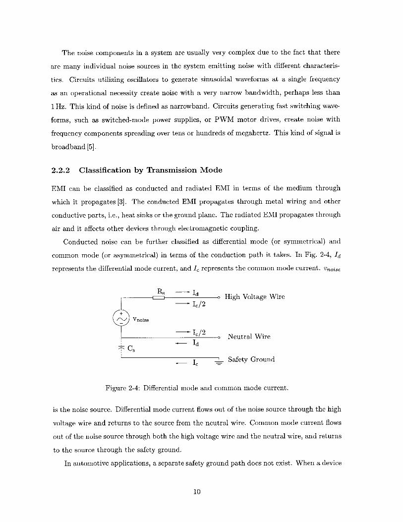
Conducted noise can be further classified as differential mode (or symmetrical) and
common mode (or asymmetrical) in terms of the conduction path it takes. In Fig. 2-4, Id
represents the differential mode current, and Ic represents the common mode current. Vnoise
R's Id High Voltage WireIc/2
+ C /vnoise
Neutral WireId
Cs;
Safety Ground
Figure 2-4: Differential mode and common mode current.
is the noise source. Differential mode current flows out of the noise source through the high
voltage wire and returns to the source from the neutral wire. Common mode current flows
out of the noise source through both the high voltage wire and the neutral wire, and returns
to the source through the safety ground.
In automotive applications, a separate safety ground path does not exist. When a device
10
is directly mounted onto the car body, the car body acts as the neutral wire. When a device
is isolated from the car body, twisted pair wires are used to connect it to the power supply,
and no local grounding is provided. For this reason, the common mode noise will not be
considered in this investigation.
For industrial and household applications, the EMI measurement is generally conducted
in two frequency bands, 0.15 MHz to 30 MHz, and 30 MHz to 300 MHz, according to the
transmission mode of the noise. For automotive applications, the two frequency bands
are from 150 kHz to 108 MHz, and from 150 kHz to 960 MHz. For different transmission
modes, different measurement methods apply. Detailed descriptions of the standards for
automotive applications are presented in Section 2.5.
2.3 Investigation and Reduction of Conducted EMI
The switching frequency for PWM dc motor drive applications is a few kilohertz up to
several tens of kHz. According to Fig. 2-3, most of the noise energy is concentrated at
the fundamental switching frequency and its immediate higher harmonics. At such low
frequencies, almost all of the electrical energy will be in the form of conducted emission,
because the relatively short wiring used in automobile applications prevent electrical signals
at these frequencies to radiate efficiently.
The level of the radiated EMI depends on the level of the conducted EMI in all frequency
ranges. Furthermore, reducing the radiated EMI requires such expensive steps as building
higher quality shielding boxes, and using expensive co-axial cables. Consequently, it is
much cheaper to reduce the radiated EMI by first eliminating the conducted EMI as much
as possible. So, reducing the conducted EMI before trying to reduce the radiated EMI is a
common practice.
Because of the time constraints on this research project and the reasons listed above,
the investigation will focus on the reduction of differential mode conducted EMI in PWM
motor drives.
2.4 Definition of Insertion Loss
The performance of an EMI filter is measured in terms of insertion loss. Insertion loss of a
filter is defined as the ratio of the powers consumed by the load in a reference circuit before
11

SignalGenerator
ZsVg ~ ZI Vb
(a)
zsVg DUT Zi Va
(b)
Figure 2-5: Insertion loss definition. (a) Reference circuit.
(b) Test item inserted.
and after the filter is inserted into the reference circuit (Fig. 2-5). It can be expressed as
IL = 10 log (bSPa
= 20 log (b (2.11)SVa
where Pb and Pa correspond to the power dissipated by the load before and after the filter
is inserted, and Vb and Va are the corresponding voltages across the load. In practice, the
reference circuit has identical source and load impedance, i.e., Zi = Z8 .
If the Z parameters or the A parameters for the filter are known, the insertion loss of
the filter can be expressed in terms of these parameters as
(Z 11 + Zs)(Zl + Z 2 2 ) - Z12Z21IL = 20Olog ( 8 Z) 2
20 log An Z + A 12 + A 21 ZsZ + A 2 2 Zs (2.12)Zs + Zi
(Please see Appendix A for the derivation of Eq. 2.12.) The Z parameters and the A
12

parameters are defined as
Vi Z11 Z12 1
V2 Z21 Z22 12
V A11 A12 V2 (2.13)
I1 A21 A22 -12
The voltage and current signals V1, I1, V2 and 12 are defined in Fig. A-2. Insertion loss is
different from attenuation in the sense that it is determined not only by the characteristics
of the circuit, but also by the source and load impedances.
2.5 Standard SAE J1113/41
Due to the nature of their operating environment, different types of applications require
different EMI limits; therefore, various EMI standards exist. For the automotive industry,
all electronic devices installed in cars sold in the United State should meet standard SAE
J1113/41.
Standard SAE J1113/41 provides details of test requirements and guidelines. Require-
ments are imposed on such things as power supply, measurement resolution bandwidth,
ground noise level, ground plane and test layout. Requirements on resolution bandwidth
and ground noise level are given in this section, and the rest will be given in the next
chapter.
Table 2.1 and Table 2.2 give minimum scan time and measurement instrument band-
width required for the measurement.
Table 2.1: Minimum scan time [6].
Band Peak Detection Quasi-peak Detection9-150 kHz Does not apply Does not apply
0.15-30 MHz 100 ms/MHz 200 s/MHz30-1000 MHz 1 ms/MHz or 100 ms/MHz 20 s/MHz
1 When 9 kHz bandwidth is used, the 100 ms/MHz value shall be used.
The frequency range specified in SAE J1113/41 is different from that specified in stan-
13
Table 2.2: Measuring instrument bandwidth (6 dB.)
Broadband NarrowbandFrequency Band Peak and Quasi-peak Peak and Average
0.15-30 MHz 9kHz 9kHz30-1000 MHz FM Broadcast 120 kHz 120 kHz30-1000 MHz Mobile Service 120 kHz 9 kHz
dards applied in industrial and household appliances. According to SAE J1113/41, the
frequency range of interest for the conducted EMI is from 150 kHz to 108 MHz and that of
the radiated EMI is in the range from 150 kHz to 960 MHz.
Table 2.3 provides the limits on conducted emission for peak and quasi-peak detection.
The limits are divided into classes. The ground noise level for EMI measurement should be
at least 6 dB below the limit specified by the test plan. When designing the filter, the proper
limit will be chosen according to the design specifications, and the difference between this
limit and the measurement results is the insertion loss needed.
14
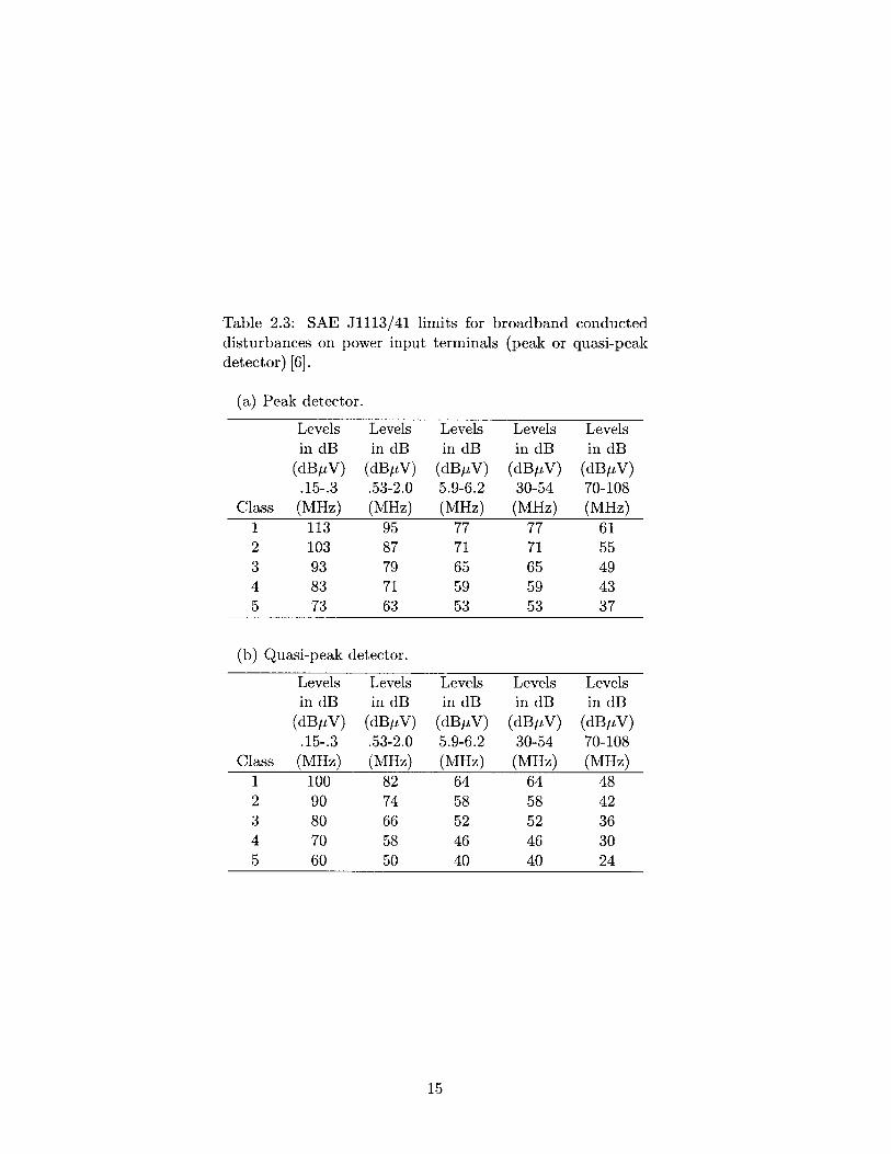
Table 2.3: SAE J1113/41 limits for broadband conducteddisturbances on power inputdetector) [6].
terminals (peak or quasi-peak
(a) Peak detector.
Class
12345
Levelsin dB
(dByiV).15-.3
(MHz)113103938373
Levelsin dB
(dByV).53-2.0(MHz)
9587797163
Levelsin dB
(dByV)5.9-6.2(MHz)
7771655953
Levelsin dB
(dByiV)30-54(MHz)
7771655953
Levelsin dB
(dByiV)70-108(MHz)
6155494337
(b) Quasi-peak detector.
Levels Levels Levels Levels LevelsindB indB indB indB indB
(dByV) (dByV) (dByV) (dByV) (dByiV).15-.3 .53-2.0 5.9-6.2 30-54 70-108
Class (MHz) (MHz) (MHz) (MHz) (MHz)1 100 82 64 64 482 90 74 58 58 423 80 66 52 52 364 70 58 46 46 305 60 50 40 40 24
15
Chapter 3
Experimental Setup
EMI measurement is a well know difficult task, because many factors can affect the cred-
ibility and repeatability of the measurement. For example, if equipment in the test setup
is not carefully isolated electrically from the environment, additional paths for the noise
signal may be introduced, and the measurement result may be higher or lower than the
actual value. Another example would be that a very noisy environment would push the
measurement result into an erroneously high level at some frequencies (this is particularly
true for radiated EMI measurement). Because of the nature of this experiment, testing
environment and equipment layout are considered very carefully.
3.1 Test Bench Layout
The test bench layout used in this experiment follows recommendations given by standard
SAE J1113/41. Figure 3-1 shows the top view of the relative positions of the equipment
on a common ground plane. The common ground plane is made with a 8' x 3' x 1/8' brass
plate.
The ground plane is crucial for correct EMI measurement for two reasons. Not only is
it a reference point with respect to which the noise spectrum is measured, but it also serves
as a shielding of the test equipment against ambient noise.
For differential mode noise measurement, all of the equipment is electrically floating
with respect to the brass plate, except the Line Impedance Stabilization Network (LISN.)
The ground terminal of the LISN is connected to the brass plate. The electrical isolation
is created by lifting all devices 40 mm from the ground plane. The following sections will
16
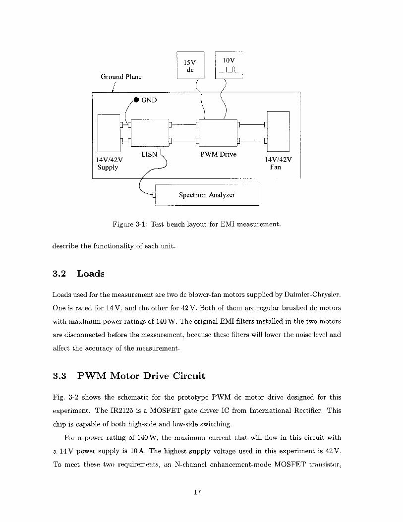
Ground Plane
15V 10Vdc JLIL
Figure 3-1: Test bench layout for EMI measurement.
describe the functionality of each unit.
3.2 Loads
Loads used for the measurement are two dc blower-fan motors supplied by Daimler-Chrysler.
One is rated for 14 V, and the other for 42 V. Both of them are regular brushed dc motors
with maximum power ratings of 140 W. The original EMI filters installed in the two motors
are disconnected before the measurement, because these filters will lower the noise level and
affect the accuracy of the measurement.
3.3 PWM Motor Drive Circuit
Fig. 3-2 shows the schematic for the prototype PWM dc motor drive designed for this
experiment. The IR2125 is a MOSFET gate driver IC from International Rectifier. This
chip is capable of both high-side and low-side switching.
For a power rating of 140 W, the maximum current that will flow in this circuit with
a 14 V power supply is 10 A. The highest supply voltage used in this experiment is 42 V.
To meet these two requirements, an N-channel enhancement-mode MOSFET transistor,
17
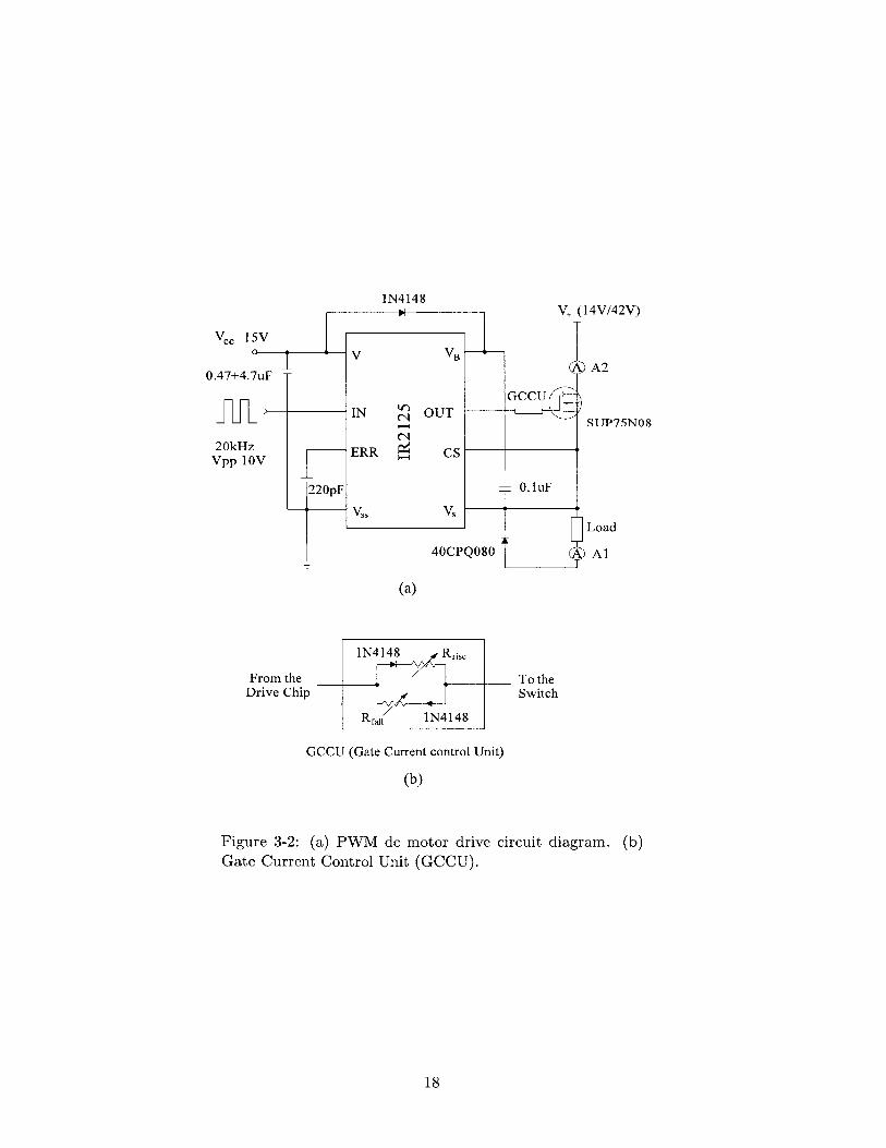
V, (14V/42V)
A2
SUP75NO8
Load
AA1
To theSwitch
GCCU (Gate Current control Unit)
(b)
Figure 3-2: (a) PWM dc motor drive circuit diagram.Gate Current Control Unit (GCCU).
18
1N4148
(a)
From theDrive Chip
(b)

SUP75NO8 by Temic Semiconductors, is used. High-side switching is adopted in this exper-
iment.
The IR2125 utilizes the bootstrap method to control the gate of the MOSFET to achieve
high-side switching. When the control signal is low, the capacitor between VB and Vs, Cb0 0 t,
is charged up by the dc power supply connected to VCC. The voltage of this dc power supply
should be between 10 V and 20 V. When the input signal is high, VB and OUT are connected
inside the IR2125, and the current flows from Cboot to the gate of the MOSFET through
VB and OUT. The switch starts to conduct once the gate-source voltage Vgs reaches its
threshold voltage, and it will remain conducting as long as Vgs is sufficiently high. Capacitor
Cboot has to be large enough to keep Vg, greater than the threshold voltage during the time
the switch is on.
A Schottky diode, 40CPQ080, connected across the inductive load provides a path for
the load current to prevent instantaneous current changes in the load when the MOSFET
is turned on and off.
The Gate Current Control Unit (GCCU) between the output pin of the IR2125 and
the gate of the MOSFET switch controls the rise and fall time during switching. The rise
and fall time directly influences the di/dt level of the current waveform, and consequently,
it affects the energy distribution of the noise in the frequency domain. A more detailed
description of the GCCU can be found in Chapter 4.
3.4 Rectangular Wave Generator and Power Supplies
The control signal of the IR2125 is provided by a rectangular wave generator with a variable
duty ratio and switching frequency. This rectangular wave generator is designed and built
around a LM555 one-shot timer IC from National Semiconductor, and the schematic of the
circuit is shown in Fig. 3-3.
The timing parameters can be determined by the following equations:
thigh = 0.67(RA) - CC (3.1)
tio = 0. 67 (RB) CC (3.2)
T thigh + tiow (3.3)
D = thigh (3.4)T
19
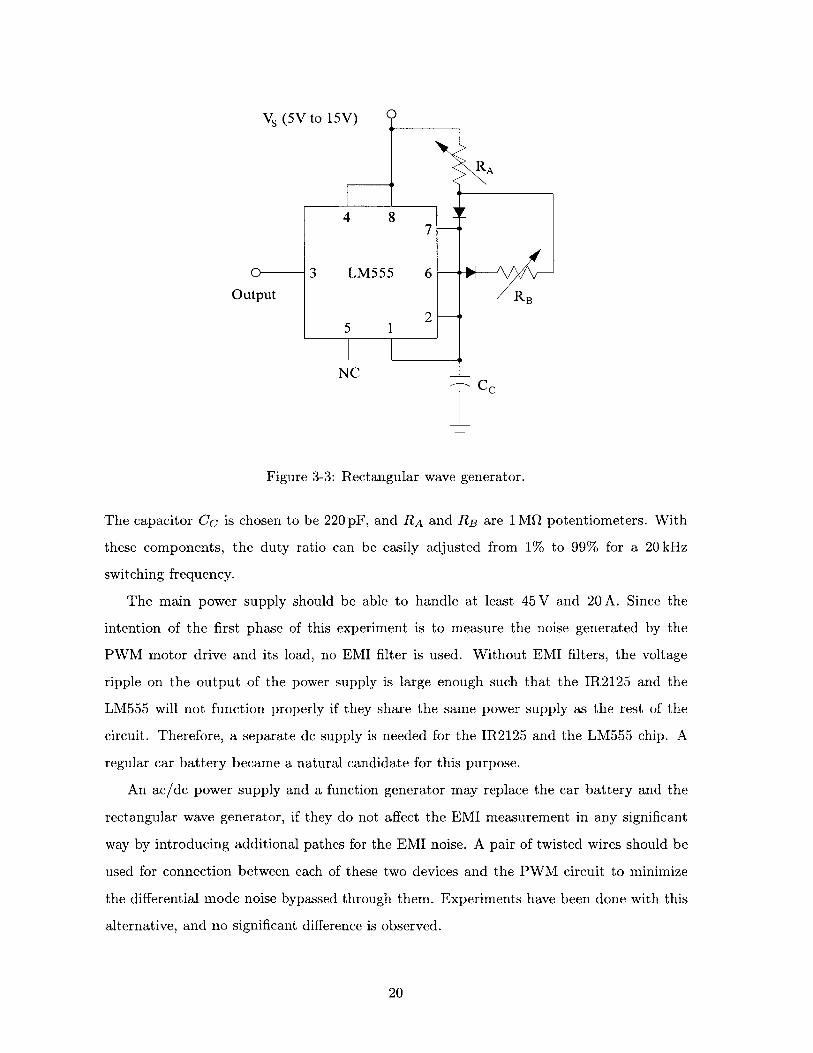
Output /RB
2-5 1
NCcc
Figure 3-3: Rectangular wave generator.
The capacitor Cc is chosen to be 220 pF, and RA and RB are 1 MQ potentiometers. With
these components, the duty ratio can be easily adjusted from 1% to 99% for a 20 kHz
switching frequency.
The main power supply should be able to handle at least 45 V and 20 A. Since the
intention of the first phase of this experiment is to measure the noise generated by the
PWM motor drive and its load, no EMI filter is used. Without EMI filters, the voltage
ripple on the output of the power supply is large enough such that the IR2125 and the
LM555 will not function properly if they share the same power supply as the rest of the
circuit. Therefore, a separate dc supply is needed for the IR2125 and the LM555 chip. A
regular car battery became a natural candidate for this purpose.
An ac/dc power supply and a function generator may replace the car battery and the
rectangular wave generator, if they do not affect the EMI measurement in any significant
way by introducing additional pathes for the EMI noise. A pair of twisted wires should be
used for connection between each of these two devices and the PWM circuit to minimize
the differential mode noise bypassed through them. Experiments have been done with this
alternative, and no significant difference is observed.
20

3.5 LISN
One of the major factors making EMI measurement a difficult task is that the impedance
of the power supply is usually unknown, or varying in a wide range as a function of time.
To make the measurement reliable and repeatable, a Line Impedance Stabilization Net-
work (LISN) is always inserted between the source and the device under test (DUT). The
functionality of the LISN is less intuitive than other units in the test setup, but it should
become clear by the end of this section.
Figure 3-4 shows a typical circuit diagram for LISN. Three major functionalities of the
L
5 pH
C1 1 pF .1 pF C 2
To Power Supply
R1 5.9 Q 50Q R2
To Load
To Measurement Instrument
Figure 3-4: Line Impedance Stabilization Network (LISN).
LISN are:
1. To create an artificial transmission line impedance for the load;
2. To prevent the EMI noise from flowing back to the power supply and
proper operation;
affecting its
3. To provide a measurement outlet for the noise measurement instrument.
At low frequencies, i.e., the switching frequency of the PWM drive and its first several
harmonics, the two capacitors, C1 and C2, have high impedances, and the inductor is
virtually a short. The LISN is transparent between the power supply and its load (Fig.
3-5(a)). At high frequencies, where the specifications are given, the LISN acts as an open
circuit between the power supply and the load because of the inductor (Fig. 3-5(b)). The
measurement is taken across the 50 Q resistor on the load side of the LISN, which is equal to
21
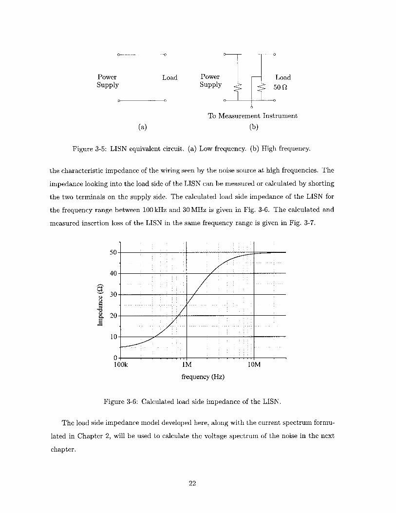
C O
PowerSupply
(a)
Load PowerSupply
To Measurement Instrument
(b)
Figure 3-5: LISN equivalent circuit. (a) Low frequency. (b) High frequency.
the characteristic impedance of the wiring seen by the noise source at high frequencies. The
impedance looking into the load side of the LISN can be measured or calculated by shorting
the two terminals on the supply side. The calculated load side impedance of the LISN for
the frequency range between 100 kHz and 30 MHz is given in Fig. 3-6. The calculated and
measured insertion loss of the LISN in the same frequency range is given in Fig. 3-7.
0i
50
40
30
20
10
0 --1 00k 1M 10M
frequency (Hz)
Figure 3-6: Calculated load side impedance of the LISN.
The load side impedance model developed here, along with the current spectrum formu-
lated in Chapter 2, will be used to calculate the voltage spectrum of the noise in the next
chapter.
22
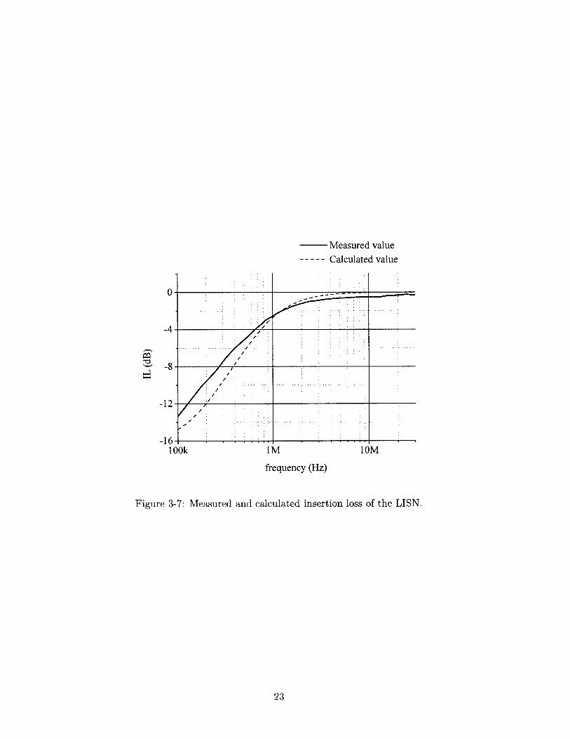
Measured value
----- Calculated value
-4
-o
-1100k IM 10M
frequency (Hz)
Figure 3-7: Measured and calculated insertion loss of the LISN.
23
Chapter 4
EMI Measurement without EMI
Filter
This chapter shows EMI measurement results without the presence of the EMI filter. Both
the frequency and time domain measurements are recorded and a detailed analysis is pro-
vided. The test setup was described in Chapter 3.
The following questions will be answered with the measurement results presented in this
chapter:
1. What level of EMI emission should be expected in the frequency range of specification
for both the 14V system and the 42V system;
2. How accurate is the theoretical model for the EMI emission developed in Chapter 2;
3. What are the key factors in determining the level of EMI emission;
4. Will a higher voltage power supply help to reduce conducted EMI;
5. What effects does the gate resistance have on the level of conducted EMI;
6. How much attenuation does an EMI filter need to meet the EMI limits of standard
SAE J1113/41 for the 42V load?
To answer these questions, both the 14V and 42V dc motors are used. Different electrical
parameters, i.e., duty ratio and gate resistance, are utilized.
24
4.1 EMI Measurement under Different Load Conditions
Although the PWM dc motor drive is rarely used in the current 14 V electrical system,
EMI measurements under this voltage will be extremely helpful for a general understanding
of electrical noise generation. These measurements can also help to answer whether any
improvement, in terms of conducted emission, can be expected by increasing the source
voltage from 14 V to 42 V, as commonly anticipated.
The switching frequency is chosen to be 20 kHz for two major reasons. The first reason
is that if the switching frequency is lower than 20 kHz, the mechanical part of the system
will produce acoustic noise audible to humans. The second reason is that by setting the
switching frequency as low as possible, the energy content of its harmonics in the frequency
range of interest can be minimized, which, in turn, lowers the insertion loss requirement for
the EMI filter to meet the specification. The lower insertion loss needed, the smaller the
filter elements required, and therefore, the cheaper the filter becomes.
The test setup is shown in Fig. 3-1. The duty ratios of the control signal are set to 50%,
30% and 20% for the measurement. The average current level is expected to decrease as
duty ratio decreases while other conditions are the same.
4.1.1 Time Domain Measurement for the 42 V Motor
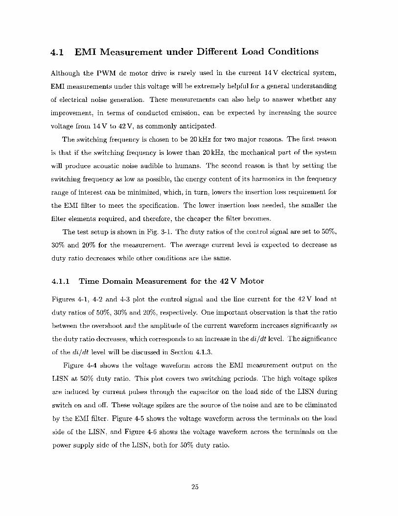
Figures 4-1, 4-2 and 4-3 plot the control signal and the line current for the 42 V load at
duty ratios of 50%, 30% and 20%, respectively. One important observation is that the ratio
between the overshoot and the amplitude of the current waveform increases significantly as
the duty ratio decreases, which corresponds to an increase in the di/dt level. The significance
of the di/dt level will be discussed in Section 4.1.3.
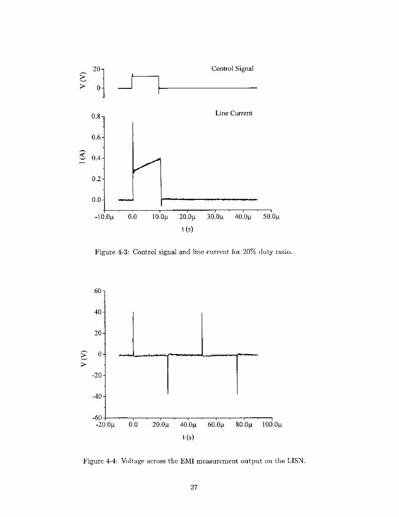
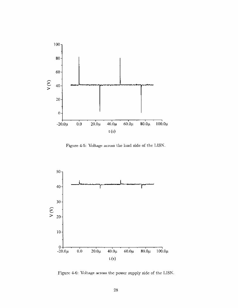
Figure 4-4 shows the voltage waveform across the EMI measurement output on the
LISN at 50% duty ratio. This plot covers two switching periods. The high voltage spikes
are induced by current pulses through the capacitor on the load side of the LISN during
switch on and off. These voltage spikes are the source of the noise and are to be eliminated
by the EMI filter. Figure 4-5 shows the voltage waveform across the terminals on the load
side of the LISN, and Figure 4-6 shows the voltage waveform across the terminals on the
power supply side of the LISN, both for 50% duty ratio.
25

Control Signal
Line Current
50.Op
t (s)
Figure 4-1: Control signal and line current for 50% duty ratio.
20 -
> 01
1.0-
0.8-
0.6-
0.4-
0.2-
0.0-
-0.2- 10 .0 p
Control Signal
Line Current
0.0 10.0p 20.0pt 30.0p 40.0i 50.0pi
t (s)
Figure 4-2: Control signal and line current for 30% duty ratio.
26
20-
0 -
1.6-
1.2-
0.8-
0.4-
0.0-
-10.0t 0.0 10.0i 20.0p 30.0p 40.0pt
-t-
20 -
> 0-]
0.8
0.6-
0.4-
0.2-
0.0-
Control Signal
Line Current
-10.0pj 0.0 1.Opt 20.0pt 30.0pt 40.0i 50.0pt
t (s)
Figure 4-3: Control signal and line current for 20% duty ratio.
-60--20.0i 0.0 20.0pt 40.0i 60.0pt 80.0i 100.0i
t (s)
Figure 4-4: Voltage across the EMI measurement output on the LISN.
27
60
40
20
0
-20
-40
100-
80-
60-
40-
20-
0-
-20.0
50-
40
30-
20-
10-
p 0.0 20.0pi 40.0p 60.0pt 80.0pt 100.0p
t (s)
Figure 4-5: Voltage across the load side of the LISN.
I 0.0 20.0p 40.0pi 60.0p 80.01 100.Op
t (s)
Figure 4-6: Voltage across the power supply side of the LISN.
28
0|-20.(
4.1.2 Time Domain Measurement for the 14 V Motor
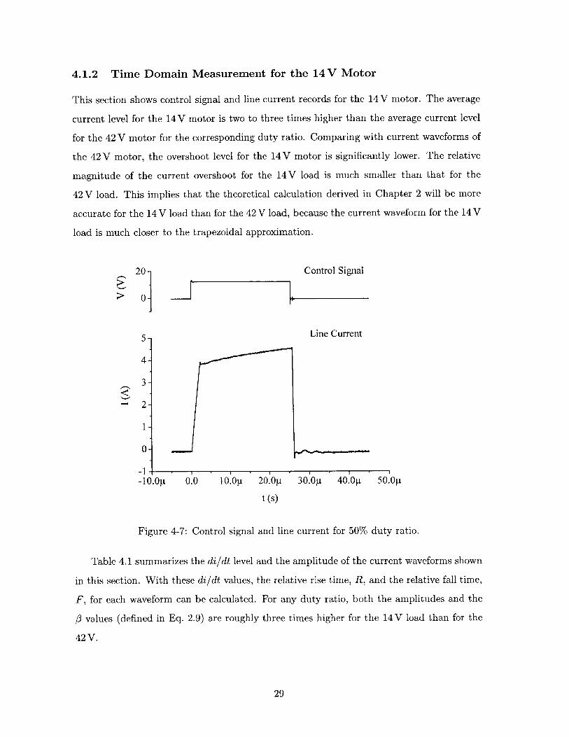
This section shows control signal and line current records for the 14 V motor. The average
current level for the 14 V motor is two to three times higher than the average current level
for the 42 V motor for the corresponding duty ratio. Comparing with current waveforms of
the 42 V motor, the overshoot level for the 14 V motor is significantly lower. The relative
magnitude of the current overshoot for the 14 V load is much smaller than that for the
42 V load. This implies that the theoretical calculation derived in Chapter 2 will be more
accurate for the 14 V load than for the 42 V load, because the current waveform for the 14 V
load is much closer to the trapezoidal approximation.
20- Control Signal
;> 0-
5- Line Current
4-
3-
-2-
1
0-
-1* . I I I
-10.0p1 0.0 10.pt 20.0p 30.0p 40.0p1 50.0pt
t (s)
Figure 4-7: Control signal and line current for 50% duty ratio.
Table 4.1 summarizes the di/dt level and the amplitude of the current waveforms shown
in this section. With these di/dt values, the relative rise time, R, and the relative fall time,
F, for each waveform can be calculated. For any duty ratio, both the amplitudes and the
/ values (defined in Eq. 2.9) are roughly three times higher for the 14 V load than for the
42 V.
29
Control Signal
Line Current
0.0 10.Opt 20.0p 30.0pt 40.0pi 50.0p
t (s)
Figure 4-8: Control signal and line current for 30% duty ratio.
Control Signal
Line Current
-10.0pt 0.0 10.0p 20.0p 30.0p 40.0p 50.0p
t (s)
Figure 4-9: Control signal and line current for 20% duty ratio.
30
20-
> 0-
2.4-
1.8-
1.2-
0.6-
0.0
-0.6 --10.0t
20 -20
>. 01
1.8-
1.2-
0.6-
0.0-
-0 | . .
waveform parameters for different loads.
ratio di(trise)/dt di(tfall)/dt Amplitude(A/ps) (A/ps) (A)
50% 11.2 8.95 1.2042 V 30% 15.9 4.62 .628
20% 17.2 2.47 .442
50% 1.87 11.9 4.5014V 30% 1.99 16.1 2.03
20% 2.30 22.1 1.33
4.1.3 Frequency Domain Measurement for Both Motors
The frequency spectrum of the noise can be easily calculated with theoretical results devel-
oped in Chapter 2. Fig. 4-10 shows the ac circuit model for the spectrum calculation, where
L
1pF --
50Q
Figure 4-10: The ac circuit model for the measurement cir-cuit. The PWM drive with its load is modeled as a currentsource.
the PWM drive circuit and its load is replaced by a current source. The dc power supply
is shorted for ac calculation. The calculation is incorrect for frequencies above 30 MHz,
because the resolution bandwidth used in this frequency range is much higher than the
switching frequency. The correct spectrum can be obtained by convolving an appropriate
window with the calculated spectrum.
Figure 4-11 shows the calculated and measured spectrums for the 14 V load at 20% duty
ratio. Current parameters used in the calculation are A =1.33 A, R =.01, F =.0012, d =.2,
and fe, = 20 kHz, which are obtained from Table 4.1. These parameters were defined in
Section 2.1. The two curves follow each other closely.
Different from the case for the 14V load, the calculated spectrum for the 42V load
31
Table 4.1: Current
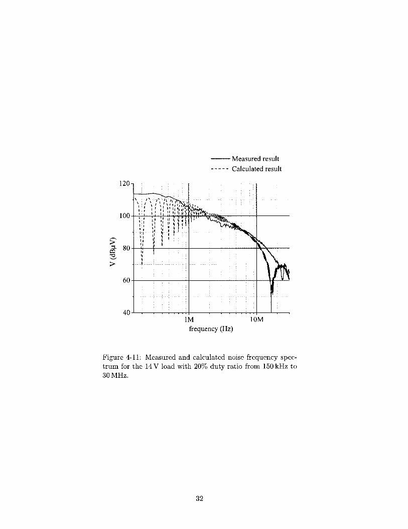
Measured result
----- Calculated result
1
100
-o
iM 10Mfrequency (Hz)
Figure 4-11: Measured and calculated noise frequency spec-trum for the 14 V load with 20% duty ratio from 150 kHz to30 MHz.
32
follows the measured result nicely at frequencies between 150 kHz and 1 MHz, but deviates
upward at higher frequencies. This is due to the overshoot that exists in the line current
for the 42 V load. The calculated spectrum for the 42 V load is not shown here.
As mentioned in Section 2.5, different resolution bandwidths should be applied to differ-
ent frequency ranges. Since the PWM drive circuit emits broadband noise, a 9 kHz resolution
bandwidth is chosen for the frequency range from 150 kHz to 30 MHz , and 120 kHz for the
frequency range from 30 MHz to 108 MHz. The frequency domain measurement results are
shown in Figures 4-12 and 4-13, corresponding to the two frequency ranges given above.
Another requirement for correct EMI measurement is that the ambient noise level should
be at least 6 dB lower than the limit specified in the test plan. The ground noise level is
shown in Fig. 4-14, and it does satisfy the requirement for meeting the Class 5 limit defined
in Table 2.3.
The theoretical analysis in Chapter 2 concludes that when R and F are much smaller
than the switching period, the spectrum distribution of the current waveform depends on
three parameters, R, F and A. Furthermore, once A is fixed, R and F are determined by
the di/dt level.
The current amplitude for the 42V load is three times smaller than that for the 14V
load for the same duty ratio (shown in Table 4.1). The magnitude of the two corresponding
spectrums at low frequencies, i.e. 150 kHz, differs by a factor of three. Since the 3 values
differ by a factor of three for the 14 V load and the 42 V load, the spectrums at high
frequencies are roughly the same for the two loads at the same duty ratio.
The measurement implies that for low frequencies, i.e., 150 kHz, the noise level is higher
for the 14 V system. For higher frequencies, however, prediction will have to be made based
on all important factors, especially, R and F. The measurement result shown in this section
is consistent with the conclusion given in Chapter 2.
4.2 EMI Measurement with Different Gate Resistance
For reasons related to the nonideal properties of the filter components, it is often desirable
to reduce EMI level at high frequencies, i.e., above 10 MHz. Since both the calculated and
measured results predict that the 3 value, or equivalently, the di/dt level determines the
EMI level at high frequencies, reducing the di/dt level can achieve the goal. One method
33

42V, 50%
120-
100-
40
14V, 30%
120-
I vv
80
60
40-
14V, 20%
20-
00-
80-
60
40iM 1OM
f (Hz)
Figure 4-12: Spectrum measured from 150 kHz to 30 MHz. The 42 V load isshown on the left column and the 14 V load is shown on the right column.Duty ratio: 50%, 30% and 20%.
34
120-
100-
-.o 80-
60
40-
42V, 30%
120-
40-
42V, 20%
120-
100-
-o80-
60
40.iM 1OM
f (Hz)
14V, 50%
10C
8C
6C
42V, 50%
90-
80
70
60
50
40-
14V, 30%
90
8C
7C
60
50
40
I-
II tI
14V, 20%
30M 40M 60M 80M lOOM
f (Hz)
Figure 4-13: Spectrum measured from 30 MHz to 108 MHz. The 42 V loadis shown on the left column and the 14 V load is shown on the right column.Duty ratio: 50%, 30% and 20%.
35
90
-o
42V, 30%
90-
80-
70-
60-
50-
40-
-o
\ A~ A .j.i
42V, 20%
90
-o
f (Hz)
v A
v v
14V, 50%
to lower the di/dt level is to increase the turn-on and turn-off time of the switch, which can
be accomplished by increasing the gate resistance of the MOSFET switch.
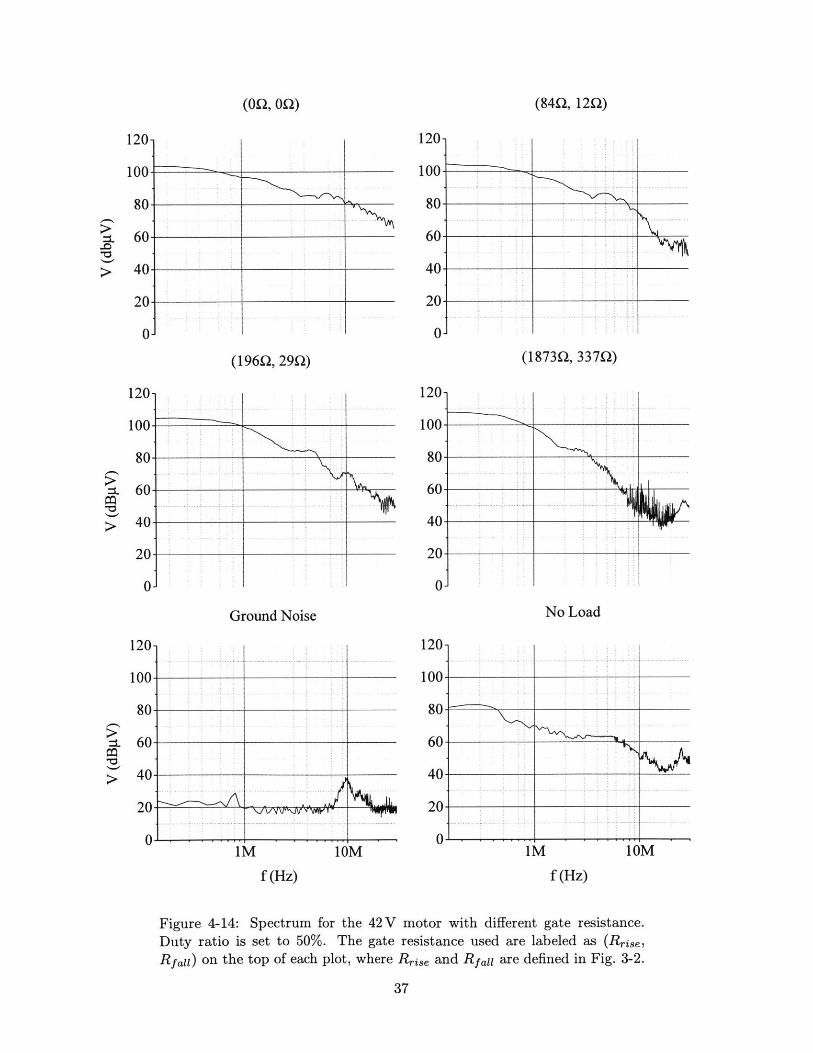
This section will present EMI measurement results of the 42 V motor with different gate
resistance. The gate resistance is controlled by the Gate Current Control Unit (GCCU).
There are two separated paths for the gate current to flow through the GCCU, and each
path is controlled by a diode. This structure of GCCU provides a way to control the rise
time and the fall time individually, so that the difference in latencies for the rising edge and
falling edge of the line current In is minimized, and the duty ratios for both Iin and the
control signal are the same.
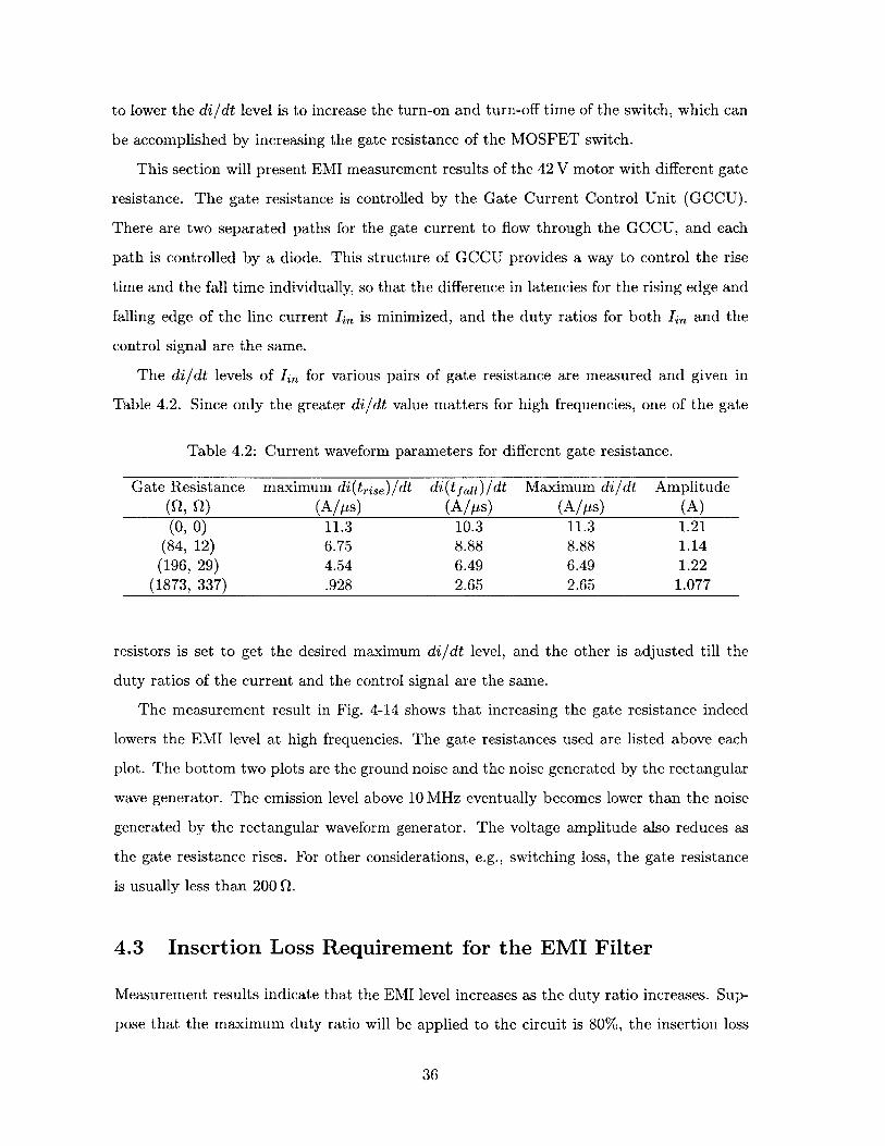
The di/dt levels of Ii, for various pairs of gate resistance are measured and given in
Table 4.2. Since only the greater di/dt value matters for high frequencies, one of the gate
Table 4.2: Current waveform parameters for different gate resistance.
Gate Resistance maximum di(trise)/dt di(tfall)/dt Maximum di/dt Amplitude(Q, Q) (A/ps) (A/ps) (A/ps) (A)(0, 0) 11.3 10.3 11.3 1.21
(84, 12) 6.75 8.88 8.88 1.14(196, 29) 4.54 6.49 6.49 1.22
(1873, 337) .928 2.65 2.65 1.077
resistors is set to get the desired maximum di/dt level, and the other is adjusted till the
duty ratios of the current and the control signal are the same.
The measurement result in Fig. 4-14 shows that increasing the gate resistance indeed
lowers the EMI level at high frequencies. The gate resistances used are listed above each
plot. The bottom two plots are the ground noise and the noise generated by the rectangular
wave generator. The emission level above 10 MHz eventually becomes lower than the noise
generated by the rectangular waveform generator. The voltage amplitude also reduces as
the gate resistance rises. For other considerations, e.g., switching loss, the gate resistance
is usually less than 200 Q.
4.3 Insertion Loss Requirement for the EMI Filter
Measurement results indicate that the EMI level increases as the duty ratio increases. Sup-
pose that the maximum duty ratio will be applied to the circuit is 80%, the insertion loss
36
(0L2, 0n)
120, 120-
100O
80
e~.1-e
f (Hz)
100
80
6C
40
I.-
20
0-
(187392 3370)
120-
I
0 ~
40
20
(1969, 29n)
.20
[00-
80
60-
40
20
0
Ground Noise
[20-
l00-
80-
60-
40-
01iM 10M
f (Hz)
Figure 4-14: Spectrum for the 42 V motor with different gate resistance.Duty ratio is set to 50%. The gate resistance used are labeled as (Rise,
Rfall) on the top of each plot, where Rrise and Rfall are defined in Fig. 3-2.
37
U-
80
60
40-- -
20-
0-i
No Load
20-
00-
60-
40-
20
0
-o
(842, 12M)
-
1M 10M
needed to meet Class 5 limits in SAE J1113/41 is shown in Fig. 4-15. Class 5 limits are
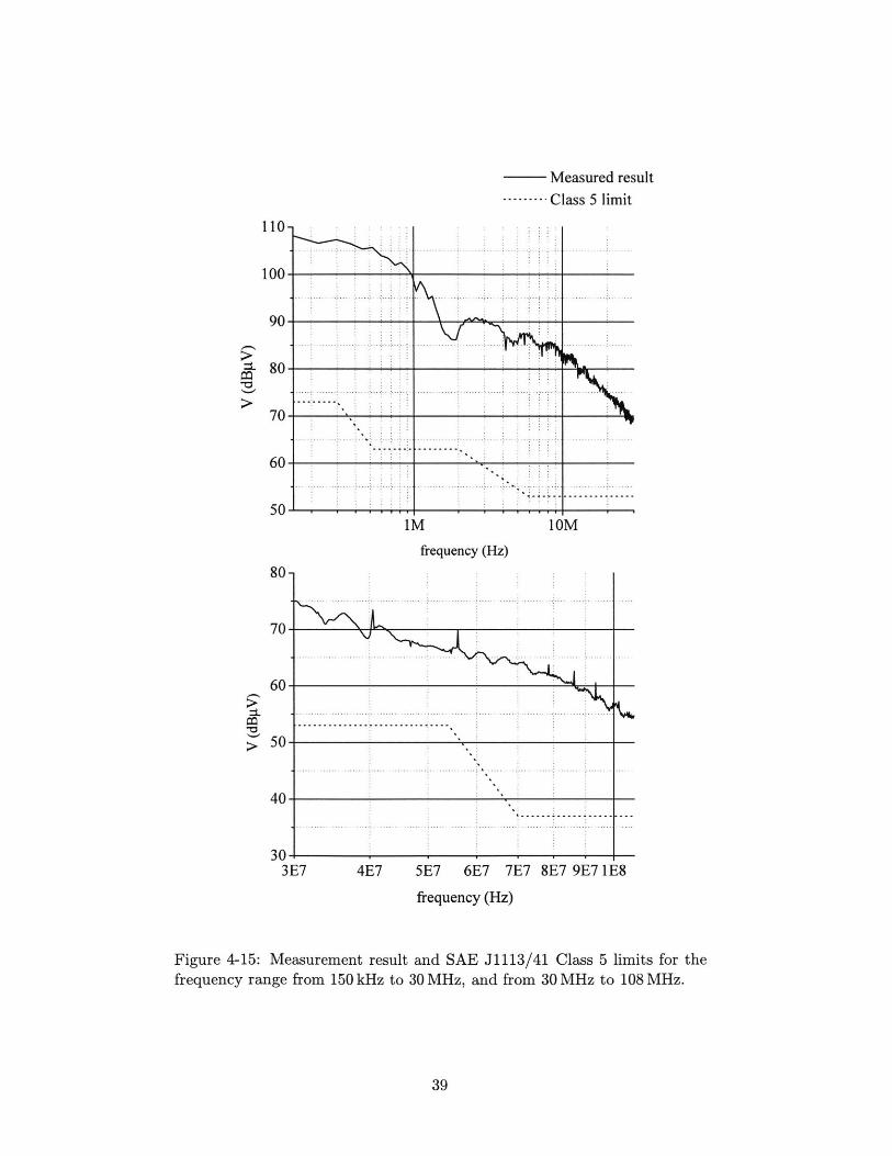
chosen because these are the limits set by the automotive industry for this application. The
plot shows that the worst frequency is at 150 kHz, where 36 dB attenuation is needed to
meet the Class 5 limit.
38
Measured result-....... Class 5 limit
110
1
0
iM 1OM
frequency (Hz)
80-
70
50
60
5C
40
30
... .... ....I ......I .... ......... ...... . . . . . . . . . . . . . . ..........
- -- -- -- -- -- -- - --- -- -- -- --- -- --
. .. .. .. .... .. .. .... ... .. ... ... ... . . ....... .. .. .. ...... ...... ... ... ..... . ...... . ....
................
.. ... ...... .... .. .... .. ... . ...... .. .... ..... . .. ...
3E7
L
4E7 5E7 6E7 7E7 8E7 9E7 1E8
frequency (Hz)
Figure 4-15: Measurement result and SAE J1113/41 Class 5 limits for thefrequency range from 150 kHz to 30 MHz, and from 30 MHz to 108 MHz.
39
......... ... ......
..... ..... ....................
Chapter 5
EMI Filter Design
There are some fundamental differences between EMI filter design and conventional filter
design. For conventional filter design, such as that used in communication, the input and
output impedances are usually known. Specifications are often given on such parameters as
ripple amplitudes in the pass band and stop band, as well as the transition width between
the pass band and stop band. For an EMI filter, on the other hand, the performance
is measured by the amount of insertion loss it can provide over its operating frequency
range. Furthermore, EMI filters in general operate over a much wider frequency range than
conventional filters do, and the flatness over the pass band or stop band is not a concern
for EMI filters , as long as they can provide sufficient insertion loss over defined frequency
ranges.
EMI filter design has often been called "Black Magic", both because EMI filter design
criteria are so flexible that there is no standard design method adopted by filter designers,
and because there are a great number of factors influencing the behavior of the filter. A de-
signer will first determine the cutoff frequency and roll-off slope needed for the filter to meet
the specifications. He will then choose a filter topology that satisfies these requirements, fix
values of some of the components, and finally solve for the rest of the components. If one set
of component values or one topology does not work, he will use a different set of components
or topology. This process will continue till all of the components are reasonably chosen and
all specifications are met. Such a process is a relatively difficult task for an inexperienced
designer. Furthermore, it does not guarantee that the design is optimal in terms of the cost
and volume of the filter.
40
This chapter will introduce some of the most popular EMI filter topologies, and discuss
the advantages and disadvantages of each topology. Constraints on filter design for this
particular type of applications will be addressed. These constraints will help to shrink
down the design scope and make the filter design a much easier task.
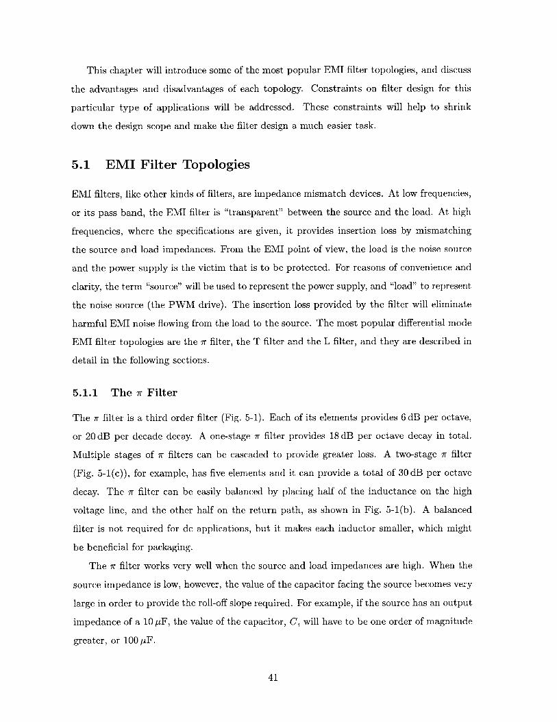
5.1 EMI Filter Topologies
EMI filters, like other kinds of filters, are impedance mismatch devices. At low frequencies,
or its pass band, the EMI filter is "transparent" between the source and the load. At high
frequencies, where the specifications are given, it provides insertion loss by mismatching
the source and load impedances. From the EMI point of view, the load is the noise source
and the power supply is the victim that is to be protected. For reasons of convenience and
clarity, the term "source" will be used to represent the power supply, and "load" to represent
the noise source (the PWM drive). The insertion loss provided by the filter will eliminate
harmful EMI noise flowing from the load to the source. The most popular differential mode
EMI filter topologies are the ir filter, the T filter and the L filter, and they are described in
detail in the following sections.
5.1.1 The 7r Filter
The 7r filter is a third order filter (Fig. 5-1). Each of its elements provides 6 dB per octave,
or 20 dB per decade decay. A one-stage 7r filter provides 18 dB per octave decay in total.
Multiple stages of 7r filters can be cascaded to provide greater loss. A two-stage 7r filter
(Fig. 5-1(c)), for example, has five elements and it can provide a total of 30 dB per octave
decay. The 7r filter can be easily balanced by placing half of the inductance on the high
voltage line, and the other half on the return path, as shown in Fig. 5-1(b). A balanced
filter is not required for dc applications, but it makes each inductor smaller, which might
be beneficial for packaging.
The ir filter works very well when the source and load impedances are high. When the
source impedance is low, however, the value of the capacitor facing the source becomes very
large in order to provide the roll-off slope required. For example, if the source has an output
impedance of a 10 pF, the value of the capacitor, C, will have to be one order of magnitude
greater, or 100 ptF.
41
L 0.5L
0.5L
(a) (b)
L L
C 2C C
(c)
Figure 5-1: (a) One-stage ir filter. (b) Balanced one-stage 7r filter. (c) Two-stage 7r filter.
The 7r filter is suitable for dc applications where the switching frequency is high enough
so that the capacitor connected to the load can supply enough current to the PWM switches
without being excessively large. In these applications, however, the source impedance should
be taken into consideration, as explained in the last paragraph.
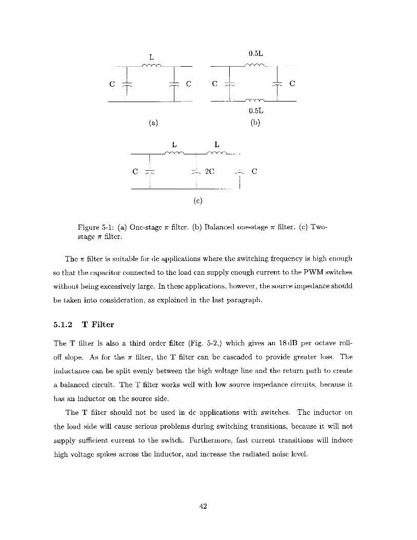
5.1.2 T Filter
The T filter is also a third order filter (Fig. 5-2,) which gives an 18 dB per octave roll-
off slope. As for the 7r filter, the T filter can be cascaded to provide greater loss. The
inductance can be split evenly between the high voltage line and the return path to create
a balanced circuit. The T filter works well with low source impedance circuits, because it
has an inductor on the source side.
The T filter should not be used in dc applications with switches. The inductor on
the load side will cause serious problems during switching transitions, because it will not
supply sufficient current to the switch. Furthermore, fast current transitions will induce
high voltage spikes across the inductor, and increase the radiated noise level.
42

L L
C
(a)
L 2L L
C - C
(b)
Figure 5-2: (a) One-stage T filter. (b) Two-stage T filter.
5.1.3 L Filter
Fig. 5-3 shows the L filter. The L filter combines advantages of both the 7r filter and the
T filter. When the capacitor is connected on the load side, the L filter can deal with a low
source impedance very well, and it has a low load side impedance. The L filter an ideal
candidate for dc applications with switches, because when the capacitor is large enough,
the filter can provide sufficient current to the switch during transitions. The only drawback
of the L filter is that it is a second order filter; therefore it does not give as much roll-off
slope as the other two types of filters do, i.e., to achieve the same amount of insertion loss
at a certain frequency with the same number of stages, the L filter will have a lower cutoff
frequency, which results in bigger components.
As for the 7r and the T filters, a higher order L filter can be constructed by cascading
several one-stage L filters together. Moreover, a two-stage 7r filter will degrade to a two-
stage L filter when the output capacitance of the source is on the same order of magnitude
as, or less than the ir filter capacitor.
43

L
Power Supply I C Load
(a)
L L
Power Supply T c C Load
(b)
Figure 5-3: (a) One-stage L filter. (b) Two-stage L filter.
5.2 EMI Filter Requirements
With a list of advantages and disadvantages of different topologies available, it does not
take very much effort to determine which topology should be applied to the PWM dc motor
drive application. Since the load of the filter is a dc switching circuit, either the L filter or
the 7r filter should be applied.
Even though the 7r filter provides a steeper roll-off slope than the L filter does, its
operation can be greatly influenced by the output impedance of the source (or the load-side
impedance of the LISN, if the goal of the filter design is to meet SAE J1113/41.) The L
filter, on the other hand, has a much higher input impedance, and therefore, it is much
more robust against the varying source impedance than the 7r filter is. In addition, the L
filter requires fewer elements than the 7r filter, and it is easier to design. Therefore, the L
filter topology (a balanced version of Fig. 5-3(a)) is chosen for this particular application.
5.3 Capacitor Value for the L Filter
Since the methodology of choosing filter elements is so flexible, it is much easier for the
designer if some constraints can be applied to the design. constraints on the value of the
capacitor for this particular application are given in this section, and the inductance required
44
to provide adequate insertion loss will be calculated in Section 5.4, after the damping circuit
is considered.
The PWM circuit and its inductive load can be modeled as a current source with a
trapezoidal waveform (Fig. 5-4). Assuming that the inductor in the L filter is large enough
A
A
t
T
Figure 5-4: Line current waveform for a typical PWM drive with a resistive load.
such that the current flowing through it is a constant equal to Iaye, the current flowing
through the current source is the sum of Iave and the current going through the capacitor.
Therefore, the charge needed to be stored in or extracted from the capacitor during different
phases of the current source can be calculated as
AQ = (Ipeak - lave) d T, (5.1)
where Ipeak is the amplitude of the current source waveform, Iave is the inductor current, d
is the duty ratio, and T is the switching period. The relationship
Av = AQC
(5.2)
implies that the capacitor has to be large enough so that the voltage ripple, Av across the
capacitor due to the stored charge variation, AQ does not affect the proper operation of
the PWM circuit. 'ave can be expressed in terms of Ipeak and d as
(5.3)Iave = Ipeakd,
45

which gives
AQ = Ipeak (d - d2 ) T. (5.4)
where Ipeak is a function of d and the load impedance. To simplify the calculation of AQ,
Ipeak is fixed to the maximum switch-on current flowing through the switch. Assuming that
the maximum duty ratio for the PWM drive is 80%, this maximum switch-on current is
measured to be 2.4 A. With Ipeak fixed, A Q reaches its maximum value at a 50% duty
ratio.
For the PWM drive to function properly, the voltage ripple across the capacitor should
be less than 15% of the dc supply voltage. With 42 V supply and a 50ps switching period,
the capacitance required for the L filter can be calculated as
C AQ
0 AV
Ipeak (d - d2 ) TAv
(2.4 A) (.5 - .52) (50ps)
(42 V)(.15)= 4.76pF. (5.5)
The capacitor value is rounded up to 5pF.
5.4 Damping and Inductor Value for the L Filter
The Q value is a very important measure for the stability of the filter and the overall
system [7]. A filter with a high Q value can cause ringing in the circuit. The voltage ripple
due to the ringing can be large enough to affect the proper operation of the circuit or even
damage the circuit.
The Q value of the filter can be reduced by adding damping to the filter. Two of the
most common damping circuits are shown in Fig. 5-5. The configuration in Fig. 5-5 (a) is
chosen for the PWM circuit, although the other configuration will work just as well. There
are two LC loops in this configuration, LC1 , and LC 2 . In general, the capacitor C2 is much
greater than C1, which gives LC 2 a much lower cutoff frequency than LC 1 . At the cutoff
frequency of LC 1 , LC 2 provides additional attenuation, and therefore, reduces the Q value
of LC 1 .
46

L
C 2
C1T R
(a)
L2 R - C
(b)
Figure 5-5: Two types of damping circuit.
In Fig. 5-5(a), C1 is the capacitor in the original L filter whose value is calculated in
the previous section. The capacitance of C2 should be at least five times larger than C1.
A 100 pF electrolytic capacitor is used for C2. R should be small to minimize the output
impedance of the filter. It is set to be 0.5 Q. The output impedance can be expressed as
= Ls(1+ RC 2 s)Z = +RC 2 s+L(C1+C2 )s 2 +LRC1C 2s 3
L sLs (5.6)
1+ f s+ L C~ s2
The gain of this filter can be expressed as
1+RC2 sGAIN = ~
AR1+ RC2 s+ L (C1 +C2) s2+LRC1 C2 3
11 (5.7)
1+is+LC~2
which can be used to calculate the inductance [7].
The measurement result in Chapter 4 shows that the greatest attenuation needed to meet
Class 5 on Standard SAE J1113/41 is 36dB, which occurs at 150 kHz. A 6dB margin is
usually recommended in EMI filter design, which increases the total attenuation at 150 kHz
to 42 dB. The inductor value is calculated using Eq. 5.7 and is equal to 27.4piH. The balanced
47
configuration of the L filter will be used, and each of the inductors will be 15pH.
5.5 Filter Component Selection and Layout
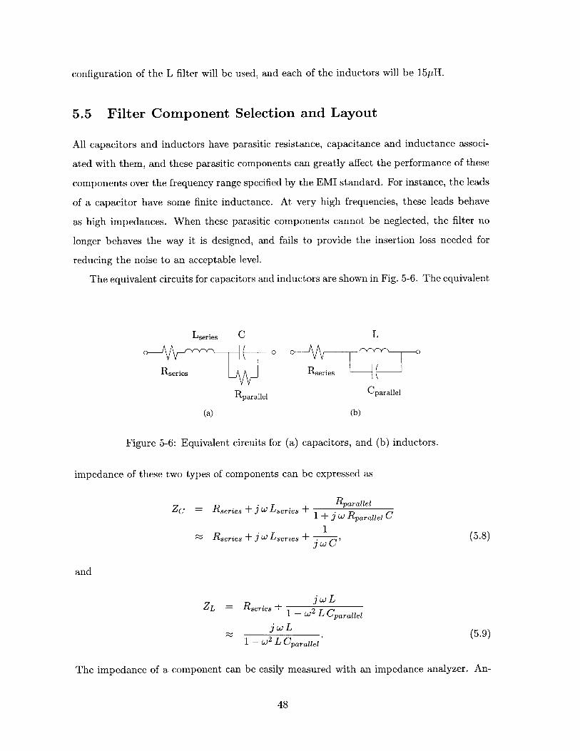
All capacitors and inductors have parasitic resistance, capacitance and inductance associ-
ated with them, and these parasitic components can greatly affect the performance of these
components over the frequency range specified by the EMI standard. For instance, the leads
of a capacitor have some finite inductance. At very high frequencies, these leads behave
as high impedances. When these parasitic components cannot be neglected, the filter no
longer behaves the way it is designed, and fails to provide the insertion loss needed for
reducing the noise to an acceptable level.
The equivalent circuits for capacitors and inductors are shown in Fig. 5-6. The equivalent
Lseries C L
Rseries Rseries
Rparallei Cparallei
(a) (b)
Figure 5-6: Equivalent circuits for (a) capacitors, and (b) inductors.
impedance of these two types of components can be expressed as
Zc = Rseries + j w Lseries + Rparauiei
1+ j W Rparaiel C1
Rseries + j w Lseries + jwC' (5.8)
and
ZL =Rseries + w1 - W2 L Cparallel
jwL (5.9)1 - W2 L Cparauel(.
The impedance of a component can be easily measured with an impedance analyzer. An-
48

other way to evaluate the performance of capacitors and inductors is to look at the insertion
loss they provide.
The performance of the inductors and capacitors depends on their physical structure
and the material used to construct them. Figure 5-7 shows usable frequency ranges for
various types of capacitors. The solid lines indicate usable frequency ranges for the regular
capacitors, and the dashed lines show those for the high quality capacitors of the same type.
Unlike capacitors, there are many parameters that characterize the behavior of inductors.
Al electrolytic
Tantalum electrolytic Mica, low-loss ceramic
Paper Metal paper I
Hi h K ceramic- - - - - - - - - - - --- :3
Polystyrene
100 101 102 103 104 105 106 107 108 109
(Hz)
Figure 5-7: Usable frequency ranges for various types of capacitors.
Consequently, different manufacturers tend to make inductor cores with various types of
material and different physical shapes. It is hard to categorize them in general [8]. Iron
powder cores are a good candidate to construct inductors for their wide operating frequency
ranges.
An electrolytic capacitor is the best choice for the 100 pF capacitor, and a film capacitor
can be used for the 5 pF capacitor. To compensate the poor high frequency performance of
the electrolytic and film capacitors, a small ceramic disk capacitor of .1 pF will be added
and described in Chapter 6. Two T68-26A iron powder cores from Micrometals are used to
construct the inductors [9].
Besides the physical structure of the components, their placement on the printed circuit
board (PCB) also has a great impact on the performance of the components. The capacitor
should be placed as close as possible to the switch, and its leads should be as short as
possible to reduce its parasitic inductance. The inductor turns should be evenly separated,
49
and as widely as possible to reduce the parasitic capacitance. The measured insertion loss
of the designed filter is shown in Fig. 5-8.
-30
-35.
-40
-45
-55 I100k IM 10M
frequency (Hz)
Figure 5-8: Insertion loss of the EMI filter.
50

Chapter 6
EMI Measurement with EMI Filter
This chapter presents EMI measurement results with the EMI filter designed in Chapter 5
inserted in the PWM drive circuit. As in Chapter 4, both the frequency and time domain
measurements are recorded, and a detailed analysis is provided.
System designers often overlook EMC issues until the last stage of the design process.
The EMI level could be unnecessarily high due to improper routing or placement of com-
ponents. Proper circuit layout and grounding can make EMI filter design much easier and
cheaper. In this chapter, the measurement result will also show how important a careful
layout is for the performance of the system. Necessary adjustments for both the filter and
the original PWM drive circuit are also discussed in detail.
6.1 EMI Measurement before Modification
The filter is inserted between the LISN and the PWM drive. Figure 3-1, repeated here as
Fig. 6-1, shows the positions of the LISN and the PWM dirve. Figure 6-2 shows the EMI
measurement for the PWM drive circuit with the filter inserted. Even though the EMI level
meets the design objective quite nicely at 150 kHz, it peaks at 8.8 MHz and gives an EMI
level 30.6 dB higher than the limit. This peak is due to the parasitic components of the
film capacitor, the excessive wiring within the PWM drive circuit, and the semiconductor
switches. These parasitic inductances and capacitances form an LC loop with a cutoff
frequency at the peak frequency.
The parasitic inductance of the wiring and the motor, along with the parasitic capacitor
of the Schottky diode (shown in Fig. 6-3) creates another LC loop with a much higher cutoff
51
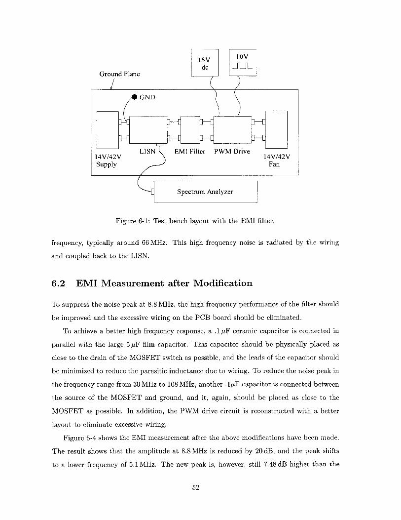
Ground Plane
15V 10Vdc L
Figure 6-1: Test bench layout with the EMI filter.
frequency, typically around 66 MHz. This high frequency noise is radiated by the wiring
and coupled back to the LISN.
6.2 EMI Measurement after Modification
To suppress the noise peak at 8.8 MHz, the high frequency performance of the filter should
be improved and the excessive wiring on the PCB board should be eliminated.
To achieve a better high frequency response, a .1 pF ceramic capacitor is connected in
parallel with the large 5 pF film capacitor. This capacitor should be physically placed as
close to the drain of the MOSFET switch as possible, and the leads of the capacitor should
be minimized to reduce the parasitic inductance due to wiring. To reduce the noise peak in
the frequency range from 30 MHz to 108 MHz, another .1pF capacitor is connected between
the source of the MOSFET and ground, and it, again, should be placed as close to the
MOSFET as possible. In addition, the PWM drive circuit is reconstructed with a better
layout to eliminate excessive wiring.
Figure 6-4 shows the EMI measurement after the above modifications have been made.
The result shows that the amplitude at 8.8 MHz is reduced by 20 dB, and the peak shifts
to a lower frequency of 5.1 MHz. The new peak is, however, still 7.48 dB higher than the
52
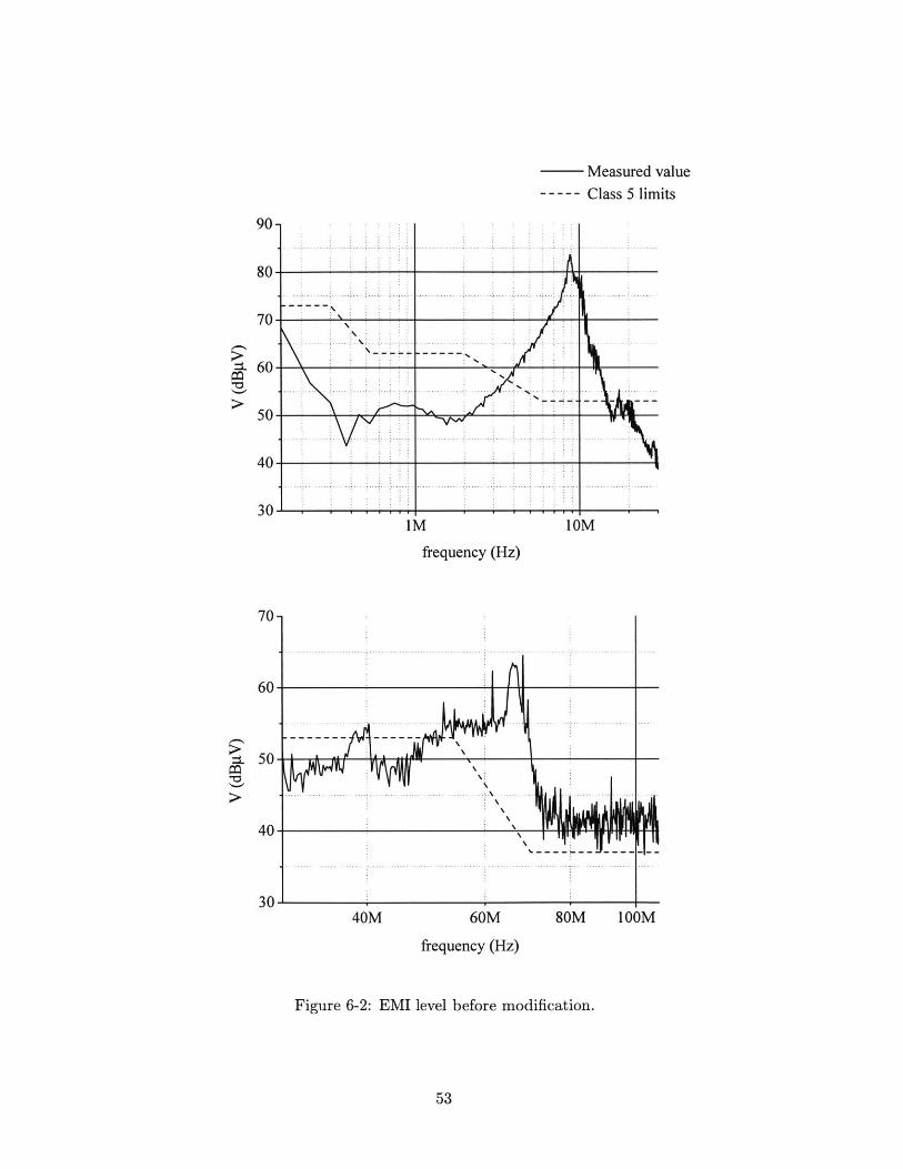
Measured value
----- Class 5 limits
IM 10M
frequency (Hz)
40M 60M 80M lOOM
frequency (Hz)
Figure 6-2: EMI level before modification.
53
90
-o
70
60
50-t
40
30
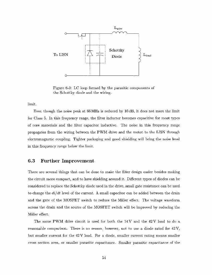
Lwire
To LISN LioadDiode o
Figure 6-3: LC loop formed by the parasitic components ofthe Schottky diode and the wiring.
limit.
Even though the noise peak at 66 MHz is reduced by 10 dB, it does not meet the limit
for Class 5. In this frequency range, the filter inductor becomes capacitive for most types
of core materials and the filter capacitor inductive. The noise in this frequency range
propagates from the wiring between the PWM drive and the motot to the LISN through
electromagnetic coupling. Tighter packaging and good shielding will bring the noise level
in this frequency range below the limit.
6.3 Further Improvement
There are several things that can be done to make the filter design easier besides making
the circuit more compact, and to have shielding around it. Different types of diodes can be
considered to replace the Schottky diode used in the drive, small gate resistance can be used
to change the di/dt level of the current. A small capacitor can be added between the drain
and the gate of the MOSFET awitch to reduce the Miller effect. The voltage waveform
across the drain and the source of the MOSFET switch will be improved by reducing the
Miller effect.
The same PWM drive circuit is used for both the 14 V and the 42 V load to do a
reasonable comparison. There is no reason, however, not to use a diode rated for 42 V,
but smaller current for the 42 V load. For a diode, smaller current rating means smaller
cross section area, or smaller parasitic capacitance. Smaller parasitic capacitance of the
54
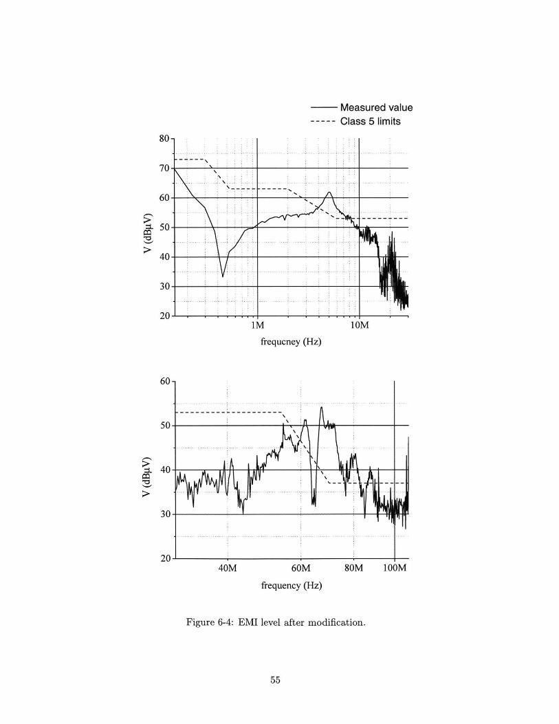
Measured value----- Class 5 limits
iM lOM
frequcney (Hz)
.' gI~ A L.
I~I. I
1 1911
40M 60M 80M looM
frequency (Hz)
Figure 6-4: EMI level after modification.
55
-o
60-
50-
-o
20
.... . ...... ..
-----------
4(
30
diode can help reduce the current spikes during turn on, which, in turn, will bring the noise
level down. Furthermore, a soft recovery diode can be used in this particular application,
because power consumption of the switch is not an issue here, as long as it does not affect
the normal operation of the switch.
The effect of the gate resistance on EMI level in the high frequency range was explained
in Chapter 4. As long as the gate resistance is not so large that it forces the MOSFET
transistor to its active region, it should be applied.
The Miller effect has some nonlinear effects on the voltage across the MOSFET switch,
which will introduce noise into the system. A capacitor on the order of a few nF can be
added between the drain and the gate of the MOSFET transistor to reduce the Miller effect.
56
Chapter 7
Conclusion
This chapter concludes this research project, and provides recommendations for future
development of the PWM dc motor drive system in automotive applications from an EMI
perspective.
This research project investigated EMI behavior of PWM dc motor drives in a typical
automotive application - blower-fan motor control. The investigation can be divided into
five phases: theoretical development, experimental test setup, EMI measurement without
filter, EMI filter design, and EMI measurement with EMI filter, and these five phases were
described in chapters 2 to 6.
Chapter 2 started with modelling the line current in a typical PWM dc motor drive
application as a trapezoidal waveform. A mathematical model of the spectrum for this line
current was then established through Fourier analysis. This model, along with a simple
LISN model, was used to calculate the EMI level for the PWM drive. One example was
given in Chapter 4.
In Chapter 3, a prototype PWM motor drive was designed and constructed. A test setup
for EMI measurements was built according to the specifications listed in SAE J1113/41.
A supporting device for accurate measurements, the rectangular wave generator, was also
built and added on to the PWM drive circuit.
Chapter 4 involved collecting and analyzing EMI measurement results for the PWM
motor drive under different load conditions and duty ratios. The effect of gate resistance
on the EMI level was also explored.
Chapter 5 focused on different aspects of EMI filter design. Such issues as topologies,
57

Q value and damping, parasitic components and frequency response of capacitors and in-
ductors were considered. An EMI filter for the prototype PWM drive was designed and
constructed.
In Chapter 6, the performance of the EMI filter built in the previous phase was evaluated.
Adjustments were made for the original PWM drive circuit to improve the high frequency
performance of the entire system.
The theoretical model developed in the second phase was found to be very accurate in
determining the EMI level of the PWM drive. The calculated result accurately matched
the measurement result.
Measurement results in the third phase show that the conducted emission of a PWM
dc motor drive depends on four parameters of the line current waveform - the relative rise
time, the relative fall time, the duty ratio and the amplitude. The first three parameters
had a great impact at frequencies higher than 1 MHz, while the last parameter determined
the EMI level over the entire frequency range. Since the amplitude is a function of duty
ratio for a particular load, the greater the duty ratio, the higher the EMI level.
For two different loads with similar power rating, the one with higher voltage rating
had lower current amplitudes for corresponding duty ratio. This indicated that the load
with the higher voltage rating has a lower EMI level than the other at low frequencies, i.e.,
150 kHz, which is the frequency requiring the greatest attenuation, or matters the most. At
higher frequencies, the other three parameters start to take effect, and the overall effect can
only be determined after a detailed calculation using the theoretical result developed in the
second phase.
The high frequency performance of the filter was limited by the packaging technology
and components available for this project, which can be easily overcome during system
integration. The behavior of the EMI filter can be correctly predicted if the parasitic
capacitance and inductance for the switches and wiring are available.
58
Appendix A
Insertion Loss Calculation
The performance of an EMI filter is evaluated by insertion loss, instead of attenuation.
Insertion loss of a device under test (DUT) is defined as
IL = 10 log (P)Pa
- 20 log( b (A.1)Va
where P and Pa are the power delivered to the load of a reference circuit before and after
the DUT is inserted into the reference circuit, and V and Va are the corresponding voltages.
Fig. 2-5 is duplicated here to show a typical way of measuring insertion loss.
A DUT can be represented by a matrix under two-port network theory, and the insertion
loss of the DUT can be calculated with this matrix. The most common matrix forms used
to calculate insertion loss are the A and the Z matrix. The A matrix is also known as the
chain matrix. It has the advantage of expressing a complicated circuit as a product of many
matrices, each of which characterizes a cascaded part of the overall circuit.
The A matrix relates the input and output voltages and current in the following way:
V Anl A 12 V2
11 ) (A21 A22 -12)
Vi, I1, V2 and 12 are defined in Fig. A-2. The Z matrix is defined as
Vi Z11 Z12 1 A3V21 Z2 )(A.3)V2Z21 Z22 I2)59

SignalGenerator
ZSg NZi %
(a)
Va
(b)
Figure A-1: Insertion loss(b) Test item inserted.
definition. (a) Reference circuit.
The relationship between the A parameters and the Z parameters are
+ 0-
V1
- 0-
DUT
1 2 <-0O+
V2
-0
Figure A-2: Voltages and currents definition for a two-portnetwork.
An1 =Z 2 1
A 1 2 = ZnIZ22 _ Z12Z 2 1
A 21
A 22
= AnZ22 - Z 1 2
1
Z 2 1
Z 2 2
Z 2 1
Eq. A.2 implies that
V2 = Z 2 1 1+Z 221 2
60
(A.4)
(A.5)
or
Z22
Z,
Va
Z21
Since
V1 = V-IiZg
= Z 11I1 + Z 1212 ,
V can be expressed as
V2Vg = (VZ + Z
2)I - Z1 2 Z,
(Zni + Zg)(Z 22 + Z1)Z21 Z1
Vb can be expressed in terms of V, as
Vb= Z VZi + Zg
and the insertion loss is
IL = 20 logV( blo(a
= 20 log (Znl+ Zg)(Z22 + Zi) - Z 12 Z2 1
(Zg + Z1)Z 21
Applying the relationship between the A parameters and Z parameters, the insertion loss
can be expressed as
IL = 20 logAn Zi + A 12 + A 2 1 Zg Z + A22Zg
Zg + Zi
This result is used to calculate the insertion loss of the LISN in Chapter 3.
61
(A.6)
(A.7)
(A.8)
(A.9)
(A.10)
(A.11)
=Z21I1 - Z22 ,
Z12 V.Zi )V

Appendix B
Matlab Code
The matlab codes listed in this Appendix are used to calculate the spectrums of the trape-
zoidal current waveform of the PWM drive and the noise, and the insertion loss of the
LISN.
The first and second functions are used to calculate the spectrums for the current wave-
form and the noise.
function trapfreq(A, R, F, d, fsw)
% File trapfreq.m
X This function calculates the spectrum of a periodic
X trapezoidal waveform.
X A: amplitude
X fsw: switching frequency
X R: rise time/period
X F: fall time/period
X d: duty ratio
X step, step1, step2: increments for different resolution
X k: harmonic number
X S: 20*logIS(k)|
X kcx: cutoff harmonic numbers;
X Si: the first segment of the envelop;
X n1: index for Si;
62

X S2: the second segment;
% n2: index for S2;
X S3: the third segment;
X n3: index for S3.
X S4: the forth segment;
X n4: index for S4.
step=1;
stepl=.2;
step2=.6;
initk=1;
finalk=3000;
% Calculate the rms value
A=A/sqrt(2);
k=initk:step:finalk;
fS=fsw*k;
ymin=10;
ymax=110;
X Calculate the spectrum
pid=pi*d;
X sinc(x)=sin(pi*x)/(pi*x)
S=20*loglO(A/pi)+120+20*loglO(abs(exp(j*pid*k)...
.*sinc(R*k)-exp(-j*pid*k).*sinc(F*k)) ./k);
X Calculate the envelop.
Sia=20*log1O(A/pi)+120+20*log1O(abs(exp(j*pid)...
*sinc(R)-exp(-j*pid)*sinc(F)));
kc1=2/sqrt((sinc(R)+sinc(F))^2*sin(pid)^2+(sinc(R)...
-sinc(F))^2*cos(pid)^2);
nl1=:step1:kcl;
63

S1=ones(1,size(n1,2));
S1=S1*Sla;
if R>F
alpha=R;
beta=F;
else
alpha=F;
beta=R;
end
kc2=1/(pi*alpha);
n2=kcl:step2:kc2;
S2a=20*loglO(A/pi)+120;
S2=S2a+20*loglO(2./n2);
kc3=1/(pi*beta);
n3=kc2:step2:kc3;
S3a=20*loglO(A)+120;
S3=S3a+20*loglO(1/pi*(1.+kc2./n3)./n3);
n4=kc3:step:finalk;
S4a=20*loglO(A)+120;
S4=S4a+20*log10((1/R+1/F)/pi^2./n4.^2);
kenv=[nl n2 n3 n4];
fenv=fsw*kenv;
env=[Sl S2 S3 S4];
figure(1)
semilogx(fS,S,'b-',fenv,env,'r-'), grid on
64
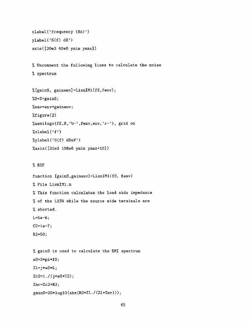
xlabel('frequency (Hz)')
ylabel('S(f) dB')
axis([20e3 40e6 ymin ymax])
X Uncomment the following lines to calculate the noise
X spectrum
X[gainS, gainenv]=LisnIM1(fS,fenv);
%S=S+gainS;
Xenv=env+gainenv;
Xfigure(2)
%semilogx(fS,S,'b-',fenv,env,'r-'), grid on
Xxlabel('f')
Xylabel('S(f) dBuV')
Xaxis([20e3 108e6 ymin ymax+10])
% EOF
function [gainS,gainenv]=LisnIM1(fS, fenv)
% File LisnIM1.m
% This function calculates the load side impedance
X of the LISN while the source side terminals are
X shorted.
L=5e-6;
C2=le-7;
R2=50;
X gainS is used to calculate the EMI spectrum
wS=2*pi*fS;
Zl=j*wS*L;
Zc2=1./(j*wS*C2);
Zsr=Zc2+R2;
gainS=20*loglO(abs(R2*Zl./(Zl+Zsr)));
65
X gainenv is used to calculate the envelop of the
% EMI spectrum
wenv=2*pi*fenv;
Zl=j*wenv*L;
Zcl=1./(j*wenv*C1);
Zc2=1./(j*wenv*C2);
Zsl=Zl+Zcl+R1;
Zsr=Zc2+R2;
gainenv=20*loglO (abs (R2*Zl . /(Zsr+Zl)));
XEOF
The third file is used to calculate the insertion loss of the LISN.
function IL=LisnIL
% File LisnIL.m
X This function calculates the insertion loss of the LISN.
X these parameters are defined in Fig. 3-4.
R1=5.9;
R2=1e4;
L=5e-6;
C1=1e-6;
C2=le-7;
% The source and load impedances of the reference circuit.
Zg=50;
Zld=50;
X The insertion loss will be calculated from 100kHz to 30MHz.
f=1e5:1e4:3e8;
w=2*pi*f;
Zl=j*w*L;
66
Zcl=1./(j*w*C1);
Zc2=1./(j*w*C2);
Zs=R1+Zcl+Zl;
X. Solve for A parameters.
A11=1+Zc2/R2;
A12=Zc2;
A22=Zc2./Zs+1;
A21=1./Zs+A22/R2;
X Use the result derived in Appendix A.
X The final result is negated to match the measurement.
IL=abs((Zld*A11+A12+A21*Zg*Zld+Zg*A22)/(Zg+Zld));
IL=-20*loglO(IL);
figure (1)
semilogx(f ,IL)
X EOF
67
Bibliography
[1] J.G. Kassakian, Hans-Christoph Wolf, J.M. Miller, and C.J. Hurton. Automotive elec-
trical systems circa 2005. IEEE Spectrum, August 1996.
[2] Laszl6 Tihanyi. Electromagnetic Compatibility in Power Electronics. IEEE Press, 1995.
[3] Mark J. Nave. Power Line Filter Design for Switched-mode Power Supplies. Van Nos-
trand Reinhold, 1991.
[4] A. Nagel and R.W. De Doncker. Some simple approximation of interference spectra.
EPE'97, 7th European Conf. on Power Electronics and Applications, September 1997.
[5] David Morgan. A Handbook for EMC Testing and Measurement. Peter Peregrinus Ltd.,
1994.
[6] SAE J1113/41. SAE Surface Vehicle Electromagnetic Compatibility (EMC) Standards
Manual. Society of Automotive Engineers, Inc., Warrendale, PA, 1997 edition, July
1995.
[7] T.K. Phelps and W.S. Tate. Optimizing passive input filter design. In Proc. of the
6th National Solid-State Power Conversion Conf., pages Gi-1-GI-10. Academic Press,
May 1979.
[8] M.F. Schlecht J.G. Kassakian and G.C. Verghese. Principles of Power Electronics.
Addison-Wesley Publishing Company, 1991.
[9] Issue H. Power Conversion & Line Filter Applications. Micrometals, Inc., Anaheim,
CA, 1995.
68