InvenSense MPU-9150 - Home - System Plus ConsultingC_R… · · 2013-05-13InvenSense –MPU-9150...
12
© 2011 by SYSTEM PLUS CONSULTING, all rights reserved. InvenSense – MPU-9150 1 21 rue La Nouë Bras de Fer – 44200 Nantes - France Phone : +33 (0) 240 180 916 - email : [email protected] - website : www.systemplus.fr November 2012- Version 2 Written by: Sylvain HALLEREAU DISCLAIMER : System Plus Consulting provides cost studies based on its knowledge of the manufacturing and selling prices of electronic components and systems. The given values are realistic estimates which do not bind System Plus Consulting nor the manufacturers quoted in the report. System Plus Consulting is in no case responsible for the consequences related to the use which is made of the contents of this report. The quoted trademarks are property of their owners.
-
Upload
nguyenthuy -
Category
Documents
-
view
240 -
download
9
Transcript of InvenSense MPU-9150 - Home - System Plus ConsultingC_R… · · 2013-05-13InvenSense –MPU-9150...
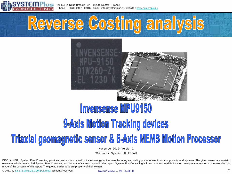
© 2011 by SYSTEM PLUS CONSULTING, all rights reserved. InvenSense – MPU-9150 1
21 rue La Nouë Bras de Fer – 44200 Nantes - France
Phone : +33 (0) 240 180 916 - email : [email protected] - website : www.systemplus.fr
November 2012- Version 2
Written by: Sylvain HALLEREAU
DISCLAIMER : System Plus Consulting provides cost studies based on its knowledge of the manufacturing and selling prices of electronic components and systems. The given values are realistic
estimates which do not bind System Plus Consulting nor the manufacturers quoted in the report. System Plus Consulting is in no case responsible for the consequences related to the use which is
made of the contents of this report. The quoted trademarks are property of their owners.
© 2011 by SYSTEM PLUS CONSULTING, all rights reserved. InvenSense – MPU-9150 2
Table of Contents
• 1. Overview / Introduction 3
– Executive Summary
– Reverse Costing Methodology
• 2. Company Profile 5
• 3. Physical Analysis 13
– Synthesis of the Physical Analysis
– Physical Analysis methodology
– Package characteristics & markings
– Package opening
– Package Opening : Dies Bonding
– Package Cross Section
– Invensense ASIC Marking
– Invensense ASIC Dimensions
– Invensense ASIC minimal dimensions
– Invensense ASIC Cross section
– Invensense ASIC Process Characteristics
– Invensense MEMS marking
– Invensense MEMS Opening
– Invensense MEMS Sensing Area
– Invensense MEMS Cap
– Invensense MEMS Process Characteristics
– Magnetometer marking
– Magnetometer Dimensions
– Magnetometer Cross Section
– Magnetometer Process Characteristics
• 4. Manufacturing Process Flow 84
– Global view
– Process Flow Accelerometer ASIC
– Process Flow MEMS Accelerometer
– Process Flow Magnetometer
– Process Flow Packaging
– Description of the Wafer Fabrication Unit
• 5. Cost Analysis 102
– Synthesis of the cost analysis
– Methodology
– Hypothesis
– Yield Synthesis
– Invensense ASIC Wafer Cost
– Invensense ASIC Die Cost Data
– MEMS Accelerometer Wafer Cost
– MEMS Accelerometer cost per Steps
– MEMS Accelerometer Equipment cost
– MEMS Accelerometer Material cost
– MEMS Accelerometer Die Cost
– Magnetometer Wafer Cost
– Magnetometer cost per Steps
– Magnetometer Material cost
– Magnetometer Die Cost
– Back-End : Package Cost
– Back-End : Package Cost Per Steps
– Back-End : Package Material cost
– Back-End : Final Test
– MPU9150 Manufacturing Cost
– Cost Analysis Evolution over yield
• 6. Estimated Selling Price Analysis 148
– Supply Chain Analysis
– Estimated Selling Price
– Price Evolution according to the yield
• Glossary
• Contacts
© 2011 by SYSTEM PLUS CONSULTING, all rights reserved. InvenSense – MPU-9150 3
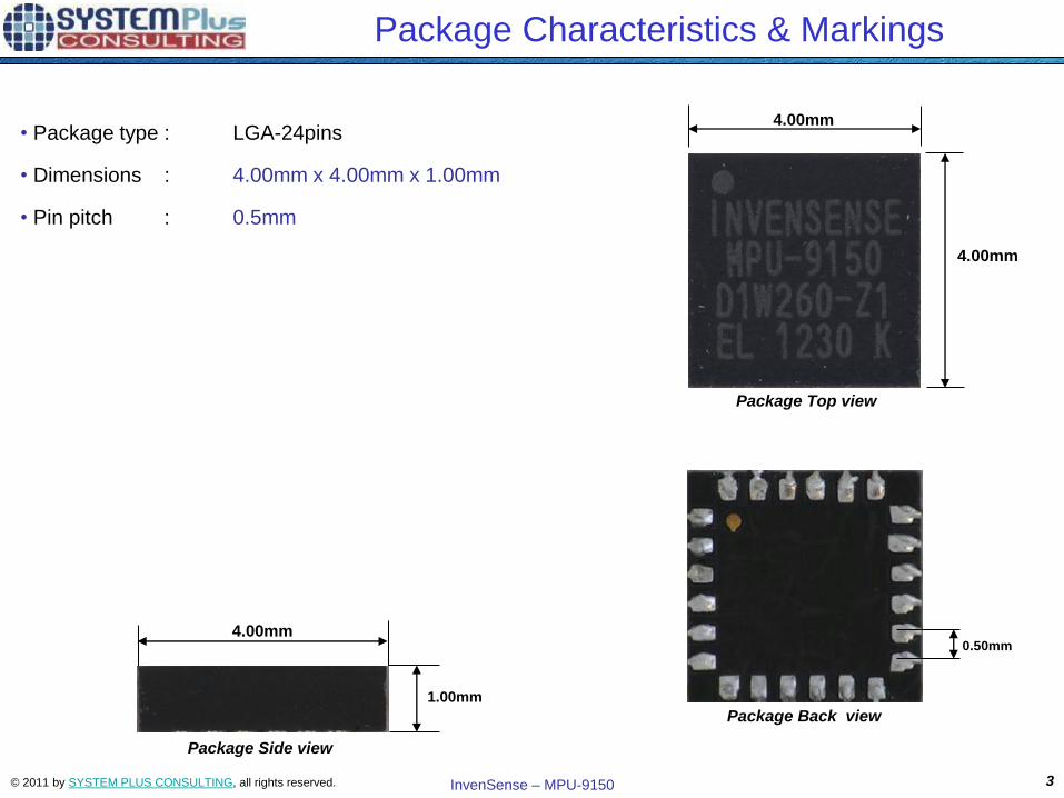
Package Characteristics & Markings
• Package type : LGA-24pins
• Dimensions : 4.00mm x 4.00mm x 1.00mm
• Pin pitch : 0.5mm
Package Top view
Package Back view
4.00mm
1.00mm
0.50mm
Package Side view
4.00mm
4.00mm
© 2011 by SYSTEM PLUS CONSULTING, all rights reserved. InvenSense – MPU-9150 4
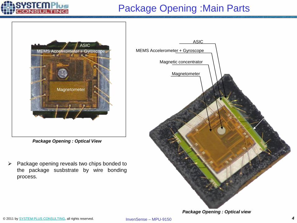
Package Opening : Optical View
Package Opening :Main Parts
Package Opening : Optical view
Package opening reveals two chips bonded to
the package susbstrate by wire bonding
process.
ASIC
Magnetic concentrator
Magnetometer
Y-axis
magnetometer
MEMS Accelerometer + Gyroscope
Magnetometer
MEMS Accelerometer + Gyroscope
ASIC
© 2011 by SYSTEM PLUS CONSULTING, all rights reserved. InvenSense – MPU-9150 5
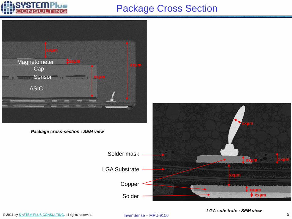
Package Cross Section
Package cross-section : SEM view
LGA substrate : SEM view
xxµm
xxµm
xxµm
xxµm
xxµm
xxµm
xxµm
xxµm xxµm
ASIC
Magnetometer Cap
Sensor
Solder mask
LGA Substrate
Copper
Solder
xxµm
© 2011 by SYSTEM PLUS CONSULTING, all rights reserved. InvenSense – MPU-9150 6
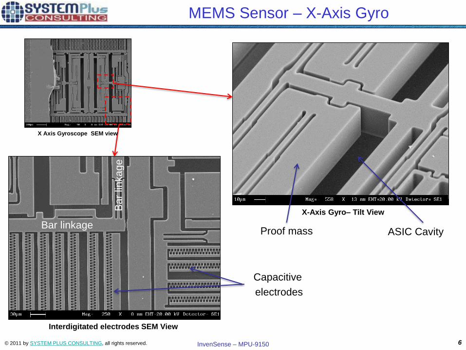
Capacitive
electrodes
Proof mass ASIC Cavity
X-Axis Gyro– Tilt View
Interdigitated electrodes SEM View
MEMS Sensor – X-Axis Gyro
Bar linkage
Bar
linkage
X Axis Gyroscope SEM view
© 2011 by SYSTEM PLUS CONSULTING, all rights reserved. InvenSense – MPU-9150 7
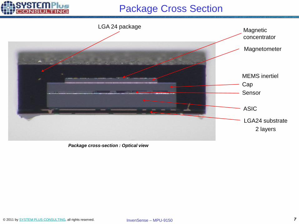
Package Cross Section
ASIC
Magnetic
concentrator
Magnetometer
MEMS inertiel
Cap
Sensor
LGA24 substrate
2 layers
LGA 24 package
Package cross-section : Optical view
© 2011 by SYSTEM PLUS CONSULTING, all rights reserved. InvenSense – MPU-9150 8
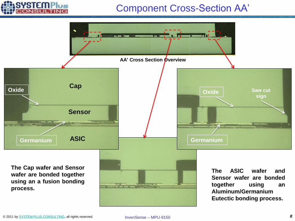
AA' Cross Section Overview
Cap
Sensor
ASIC
The ASIC wafer and
Sensor wafer are bonded
together using an
Aluminum/Germanium
Eutectic bonding process.
Germanium
The Cap wafer and Sensor
wafer are bonded together
using an a fusion bonding
process.
Oxide
Component Cross-Section AA’
Saw cut
sign
Germanium
Oxide
© 2011 by SYSTEM PLUS CONSULTING, all rights reserved. InvenSense – MPU-9150 9
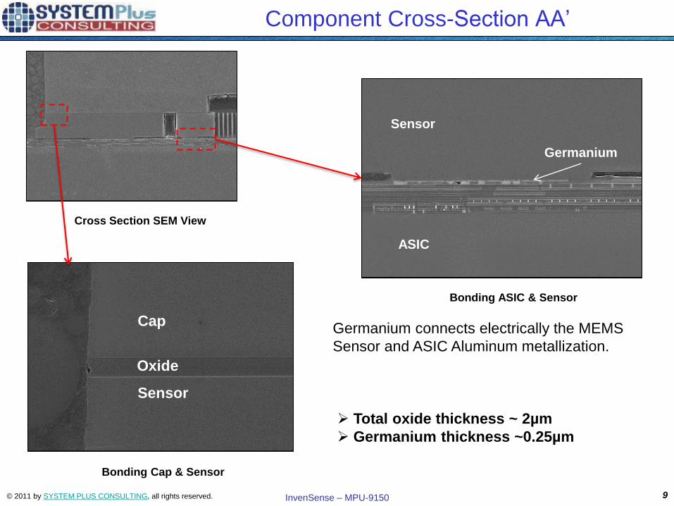
Bonding Cap & Sensor
Bonding ASIC & Sensor
Cross Section SEM View
Cap
Sensor
Oxide
Total oxide thickness ~ 2µm
Germanium thickness ~0.25µm
Germanium
Sensor
ASIC
Component Cross-Section AA’
Germanium connects electrically the MEMS
Sensor and ASIC Aluminum metallization.
© 2011 by SYSTEM PLUS CONSULTING, all rights reserved. InvenSense – MPU-9150 10
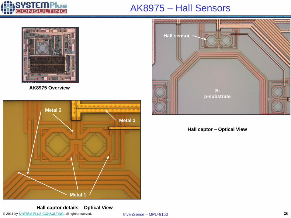
AK8975 – Hall Sensors
AK8975 Overview
Hall captor details – Optical View
Hall captor – Optical View
Metal 1
Metal 2
Metal 3
Si
p-substrate
Hall sensor
© 2011 by SYSTEM PLUS CONSULTING, all rights reserved. InvenSense – MPU-9150 11
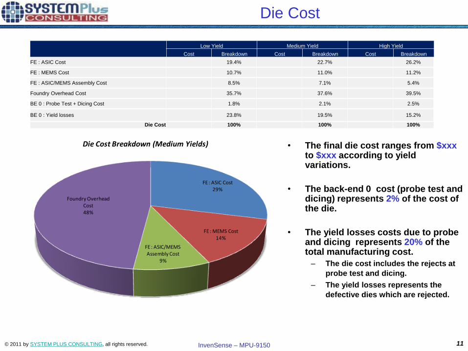
Die Cost
• The final die cost ranges from $xxx to $xxx according to yield variations.
• The back-end 0 cost (probe test and dicing) represents 2% of the cost of the die.
• The yield losses costs due to probe and dicing represents 20% of the total manufacturing cost.
– The die cost includes the rejects at
probe test and dicing.
– The yield losses represents the
defective dies which are rejected.
Low Yield Medium Yield High Yield
Cost Breakdown Cost Breakdown Cost Breakdown
FE : ASIC Cost29%
FE : MEMS Cost14%
FE : ASIC/MEMS Assembly Cost
9%
Foundry Overhead Cost48%
Die Cost Breakdown (Medium Yields)
FE : ASIC Cost 19.4% 22.7% 26.2%
FE : MEMS Cost 10.7% 11.0% 11.2%
FE : ASIC/MEMS Assembly Cost 8.5% 7.1% 5.4%
Foundry Overhead Cost 35.7% 37.6% 39.5%
BE 0 : Probe Test + Dicing Cost 1.8% 2.1% 2.5%
BE 0 : Yield losses 23.8% 19.5% 15.2%
Die Cost 100% 100% 100%
© 2011 by SYSTEM PLUS CONSULTING, all rights reserved. InvenSense – MPU-9150 12
• Reverse costing analysis represents the best cost/price evaluation given the publically
available data, completed with industry expert estimates.
• Given the hypothesis presented in this analysis the major sources of correction would lead to
a +/- 10% correction on the manufacturing cost (if all parameters are cumulated)
• IC +/- 8%
• MEMS +/- 5%
• Packaging +/- 10%
• Test +/- 20%
• These results are open for discussion. We can re-evaluate this component with your
information. Please contact us:
Conclusion