Introduction to Digital Designangelov/VHDL/VHDL...The world is to a good approximation analogue •...
77
© V. Angelov VHDL-FPGA@PI 2013 1 Introduction to Digital Design
Transcript of Introduction to Digital Designangelov/VHDL/VHDL...The world is to a good approximation analogue •...

© V. Angelov VHDL-FPGA@PI 2013 1
Introduction to Digital Design

© V. Angelov VHDL-FPGA@PI 2013 2
Introduction to Digital Design
•
Why digital processing?•
Basic logical circuits, first conclusions
•
Combinational circuits–
Adder, multiplexer, decoder ...
•
Sequential circuits–
Circuits with memory
–
State machine, synchronous circuits•
General structure of a digital design–
Top-down
–
Hardware/software
© V. Angelov VHDL-FPGA@PI 2013 3
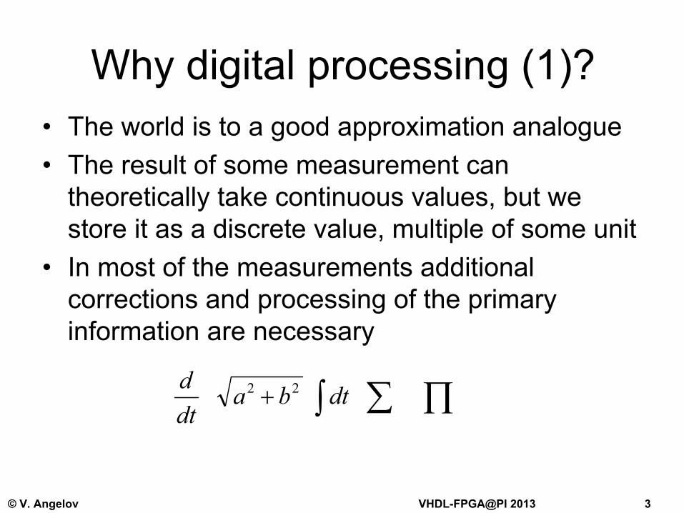
Why digital processing (1)?•
The world is to a good approximation analogue
•
The result of some measurement can theoretically take continuous values, but we store it as a discrete value, multiple of some unit
•
In most of the measurements additional corrections and processing of the primary information are necessary
∏∑∫+ 22 dtbadtd

© V. Angelov VHDL-FPGA@PI 2013 4
Why digital processing (2)?•
Block diagram of some measurement device
AD
Digital Proc.Analog
Noise, Disturbances, Nonlinearity, Temperature, Supply voltage
Discretization error,
Nonlinearity
Rounding errors
•
How to arrange the full processing in order to get the best results?
© V. Angelov VHDL-FPGA@PI 2013 5
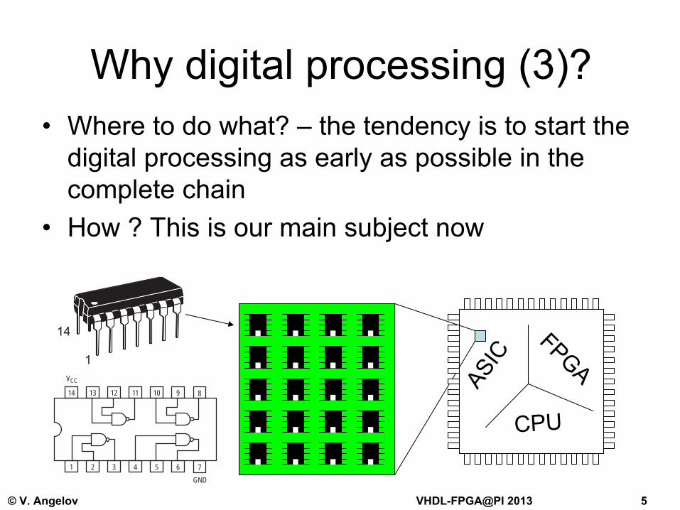
Why digital processing (3)?•
Where to do what? –
the tendency is to start the
digital processing as early as possible in the complete chain
•
How ? This is our main subject now
ASIC
FPGA
CPU14 13 12 11 10 9
1 2 3 4 5 6
VCC
8
7
GND
14
1

© V. Angelov VHDL-FPGA@PI 2013 6
Notations of the logic elements
•
The most used are shown below•
Frequent use of non-standard symbols
YAB
1AB
& Y 1AB
Y
Y=(A*B)
NOT
Y
A B Y0 0 00 1 11 0 11 1 1
A
Y
OR
A
B
XNOR
BY=(A+B)
AY
Y
B B
A B Y0 0 00 1 01 0 01 1 1
OR
A
A
A
Y = A
Y
B
A
NORXOR
Y
AA
AND
B
AND
A B Y0 0 00 1 11 0 11 1 0
B
NAND
B
© V. Angelov VHDL-FPGA@PI 2013 7
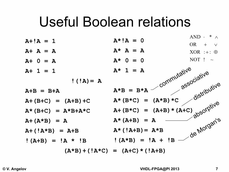
Useful Boolean relationsA+!A = 1
A+ A = A
A+ 0 = A
A+ 1 = 1
!(!A)= A
A+B = B+A
A+(B+C) = (A+B)+C
A*(B+C) = A*B+A*C
A+(A*B) = A
A+(!A*B) = A+B
!(A+B) = !A * !B
(A*B)+(!A*C) = (A+C)*(!A+B)
A*!A = 0
A* A = A
A* 0 = 0
A* 1 = A
A*B = B*A
A*(B*C) = (A*B)*C
A+(B*C) = (A+B)*(A+C)
A*(A+B) = A
A*(!A+B)=
A*B
!(A*B) = !A + !B
commutative
associative
distributive
absorptive
de Morgan's
~ ! NOT :: XOR
OR * AND
⊕+∨+∧⋅

© V. Angelov VHDL-FPGA@PI 2013 8
NAND or NOR can do everything…
NAND
NAND
NAND
NOR
NAND
NAND
NOR
NOR
NOT
NANDAND
NOR
NOROR
NOR
with NAND with NOR

© V. Angelov VHDL-FPGA@PI 2013 9
XOR with NAND or NOR
XOR
= =
A :+: B = A*!B + !A*BA + B = !(!A*!B)
OR
=
(de Morgan)
A:+:B = (A + B)*(!A + !B)=(A + B)*!(A * B)
(de Morgan)

© V. Angelov VHDL-FPGA@PI 2013 10
Simplifying Boolean expressions
F=A*!C + A*!B + !A*B*!C + !A*!B = !C*(A+!A*B) + !B = !C*(A+B)+!B
=
= !C*A+!C*B+!B = A*!C + !B + !C = !B + !C A+(A*B) = AA+(!A*B)= A+B
F=A*!C + A*!B + !A*B*!C + !A*!BFor
A=0 F=B*!C +!B = !B+!C
For
A=1 F=!C+!B
F=A*!C + A*!B + !A*B*!C + !A*!BFor
B=0 F=A*!C + A + !A = 1
For
B=1 F=A*!C + !A*!C = !C
F(a1
, a2
, …
aN
) = = a1
*F(1, a2
, …
aN
) + !a1
*F(0, a2
, …
aN
)01
F(0, a2
, …
aN
)
a1
FF(1, a2
, …
aN
)
With 4:1 mux, two variables can be eliminated

© V. Angelov VHDL-FPGA@PI 2013 11
What kind of logical elements do we need?
•
Exactly like a house, that can be built using many identical small bricks, one logical circuit can be built using many identical NOR (OR-
NOT) or NAND (AND-NOT) elements•
For practical reasons it is much better to have a rich set of different logical elements, this will save area and power and will speed up the circuit
VCC

© V. Angelov VHDL-FPGA@PI 2013 12
•
If the function is more frequently 1, it is better to calculate the inverted function in order to have less terms:
Sum of products representation
•
Truth table
Y = !A*!B*!C + !A*B*C + A*!B*C + A*B*!C + A*B*C
Y = ! ( !A*!B*C + !A*B*!C + A*!B*!C )
A B C Y0 0 0 10 0 1 00 1 0 00 1 1 11
0 0 0
1 0 1 11 1 0 11 1 1 1
A
C
CB
A
B
CB
Y
A

© V. Angelov VHDL-FPGA@PI 2013 13
Karnaugh Map (K-Map) with 3 signals
Y = !A*!B*!C+!A*B*C+A*!B*C+A*B*!C+A*B*C
A
A
C C
B BB
1
1
1
1 1
Y = !A*!B*!C + A*B + A*C + B*C
A
A
C C
B BB
1
11
1Y = A*!B + !A*C
Y =!B*C+A*!B*!C+!A*!B*C+!A*B*C
00
0
00
00

© V. Angelov VHDL-FPGA@PI 2013 14
K-Map with 4 signals
A
A
C C
D DD
B
1 1
1
1
1 1
0
0
0 0
0
0
0
0
0
0
F = !B*!D + A*!C*!D + !A*B*!C*DA*!C*!D
!B*!D
The four corner cells can be combined together as !B*!D
The two cells bottom left can be combined as A*!C*!D
One minterm
remains !A*B*!C*D
Finally we get:

© V. Angelov VHDL-FPGA@PI 2013 15
K-Map with don't care
A
A
C C
D DD
B
1 1
1
1
1 1
x
x
x x
x
0
0
0
0
0
!B*!D
!C*!D
!A*B
!A*!C
F = !B*!D + !C*!D + !A*!C
F = !B*!D + !C*!D + !A*B
If the function is not used in some combinations (x -
don't
care) of the input signals, we are free to replace any x with 0 or 1.
In this example we have two options to include the minterm
!A*B*!C*D

© V. Angelov VHDL-FPGA@PI 2013 16
K-Map for XOR
A
A
C C
D DD
B
0 1
0
0
1 0
1
1
1 0
0
0
1
1
0
1
F = A :+: B :+: C :+: D
When going from one field to any neighbour field in the K-
map, only ONE signal is changed (Gray code, see later) but the output toggles.As can be seen, this prevents any optimization, the function can be built by 8 product terms.
In the general case of XOR between N signals, the number of product terms needed is 2N-1! Actually XOR is the worst function to be implemented as sum of products.

© V. Angelov VHDL-FPGA@PI 2013 17
Conclusions(1) –
PAL/CPLD/HDL
•
The sum of products representation was a good move! It seems to be a universal method (with some exceptions) to build any logical function –
PAL and CPLD•
Drawing of the circuit is tedious and not very reliable!
•
Writing of equations seems to be easier and more reliable → languages to describe hardware (HDL -
hardware description
language)

© V. Angelov VHDL-FPGA@PI 2013 18
Conclusions(2) – ASICAnother possibility is to have many different logic functions. Here are shown only a small subset of the variations with AND-OR-
NOT primitive functions available in a typical ASIC library
All about 130 units + with different fanout
capability
AO32
AO22
AO31
AO211AOI211
AO31M10
AO22M10
AO22M20AOI22M10
AO21M10
AO21M20

© V. Angelov VHDL-FPGA@PI 2013 19
Conclusions(3) – LUT/FPGA•
Another possible architecture for logical functions is to implement the truth table directly as a ROM
•
When increasing the number of the inputs N, the size of the memory grows very quickly as 2N!
•
If we have reprogrammable small memory blocks (LUT - Look Up Table), we could easily realize any function –
the only limit is the number of the input signals
•
For larger number of inputs we need to do something
LUT
abc
F(a, b, c)0 0 0 : 10 0 1 : 00 1 0 : 00 1 1 : 1…
The FPGAs
contain a lot of LUT with 4 to 6 inputs + something more

© V. Angelov VHDL-FPGA@PI 2013 20
Conclusions(4) – FPGA•
Another possible architecture is to use multiplexers
•
Examples of simple 2-input logical functions built with 2:1 multiplexer
This approach is used in some FPGA architectures
B
B
A
A
A
'1'
B
B
B
Y
Y
1
0
Y 1
Y0
A
1
A
Y
B
A
0
1
Y'1'
0
A
'0'
'0'A
Y
B
=
=
=
=

© V. Angelov VHDL-FPGA@PI 2013 21
Combinational circuits•
... are the circuits, where the outputs depend only on the present values of the inputs
•
Practically there is always some delay
in the reaction of the circuit, depending on the temperature, supply voltage, the particular input and the state of the other inputs
•
it is good to know the min and max values (worst/best case) A1
AN
F(A1
, A2
, ... AN
)

© V. Angelov VHDL-FPGA@PI 2013 22
Special combinational circuits - multiplexer
•
Used to control data streams –
several data sources to a single receiver
0123
I1I2
I0
I3
S1..0
Y
S Y0 I01 I12 I23 I3
Y = !S[1]*!S[0]*I[0]+!S[1]* S[0]*I[1]+S[1]*!S[0]*I[2]+S[1]* S[0]*I[3]
I3
Y
S0
I2
I0
I1
S1
© V. Angelov VHDL-FPGA@PI 2013 23
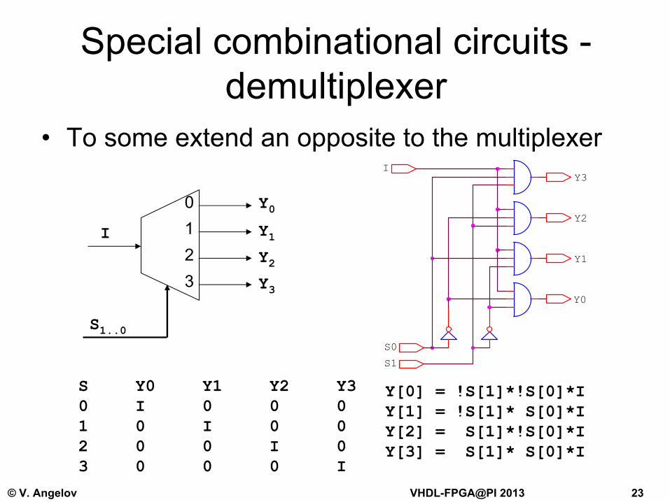
Special combinational circuits - demultiplexer
•
To some extend an opposite to the multiplexer
0123
Y1Y2
Y0
Y3
S1..0
I
S Y0 Y1 Y2 Y30 I 0 0 01 0 I 0 02 0 0 I 03 0 0 0 I
Y[0] = !S[1]*!S[0]*IY[1] = !S[1]* S[0]*IY[2] = S[1]*!S[0]*IY[3] = S[1]* S[0]*I
Y1
Y0
S1
I
S0
Y2
Y3

© V. Angelov VHDL-FPGA@PI 2013 24
Special combinational circuits - adder
•
Add/subtract –
for more than some bits here it is not practical to use the sum-of-products approach (Why?)
•
Binary system–
Integer numbers ≥
0 (unsigned)
–
Integer numbers –
positive and negative (signed) -
later–
Adding of binary integer numbers, carry
•
Building blocks–
Half-
and Full-
adder
1011011010001
+ ?To calculate the most significant bit of the result we have to go through all the other bits, the carry jumps from bit to bit and this takes time!

© V. Angelov VHDL-FPGA@PI 2013 25
Half-
and Full-
adder
A + B = 2·Cout + S
A + B + Cin
= 2·Cout + S
AB
SCout
FACin
AB
SCo
Ci
AB
SCout
HAAB
SCo
Half-adder
Full-adder
B
SA
Cout
B
A
Cin
S
Cout

© V. Angelov VHDL-FPGA@PI 2013 26
4 bit ripple carry adder
1111000110000
+ A3..0B3..0S4..0
A0B0
S0HA
A1B1
S1FA
A2B2
S2FA
A3B3
S3FAS4
Ripple carry adder
Co0
Co1
Co2
AB
SCo
Ci
AB
SCo
Ci
AB
SCo
Ci
AB
SCo
A
B
S[0]
CO[0]
S[1]
CO[1]
S[2]
CO[2]
S[3]
S[4]
0 F
0 1

© V. Angelov VHDL-FPGA@PI 2013 27
Signed integers•
One’s complement –
invert all bits of A
to get the negative of A
–
The 0
has two representations +0
and -0.–
Not practical for mathematical operations
•
Two’s complement –
invert all bits and add 1–
The sum of A
and (not A +1)
is 2N
but expressed with N
bits is 00..00
=> -A=2N-A
–
All numbers from 00..00
to 01..11
are positive (0
to 2N-1-1)–
All numbers from 11..11 (-1)
to 10..00 (-2N-1)
are negative, the
MSB is 1
when the number is negative–
The full range is asymmetric, from -2N-1
to +2N-1-1
(for 8 bits, from -128
to +127). Note that the VHDL Integer
is symmetric: from
-(231-1)
to +(231-1)
–
Before doing mathematical operations with two signed numbers with different length, the shorter must be sign-extended to the length of the other

© V. Angelov VHDL-FPGA@PI 2013 28
Two’s complement – a closer look
•
Let A
be a positive integer:
•
Then the negative of A
is
•
Subtracting 2N
from both sides yields ( ):
•
In two’s complement the MSB has weight -2N-1 instead of +2N-1
–
note that this is valid for both
positive and negative numbers!
0 ,2 1
1
0== −
−
=∑ N
N
k
kk aaA
1 , 222 as drepresente 1
1
0
1
0==−− −
−
=
−
=∑∑ N
N
k
kk
N
k
kk
N bbaA
11
2
0
11
2
0
1
0
1
022222222 −
−
−
=
−−
−
=
−
=
−
=
−=−+=−=−=− ∑∑∑∑ NN
N
k
kk
NNN
N
k
kk
NN
k
kk
N
k
kk bbbbbaA
11 =−Nb

© V. Angelov VHDL-FPGA@PI 2013 29
Carry, borrow
•
For unsigned integers, carry out = 1 means, that–
when adding A+B
the result is above 2N-1
–
when subtracting A-B, B
is larger than A, in this case we speak of borrow
1011 110110 610001 1
+ 0011 30110 611101 13
-
carryborrow

© V. Angelov VHDL-FPGA@PI 2013 30
Carry, borrow, overflow
•
For signed integers, carry output = 1 is not necessary bad
•
but
1011 -50110 610001 1
+ 0011 30110 611101 -3
-
carryborrow
1011 -51010 -610101 5
+ 0011 31010 -611001 7
-
carryborrow
correct
wrong
Overflow = carry out XOR carry between the last two bits

© V. Angelov VHDL-FPGA@PI 2013 31
Correct Wrongpos + pos →
pos neg
neg + neg →
neg pospos –
neg →
pos neg
neg –
pos →
neg pos
Overflow
•
For signed integers, overflow can be detected by the wrong sign of the result:
pos + negpos –
pos
neg –
negAlways correct
This is overflow!
The MSB is 1 for the negative numbers and 0 for the positive (incl. 0), so one can detect the overflow only using the MSBs
of
the two operands and of the result

© V. Angelov VHDL-FPGA@PI 2013 32
Subtracting using an adder
•
Add/subtract with two’s complement numbers can be done exactly like with unsigned integers
•
For N-bit signed:A–B=A+(2N–B)=A+two’s_complement(B)
=B
ACin
NOT
'1'
B
A

© V. Angelov VHDL-FPGA@PI 2013 33
A_GT_B
B2
B0
A1
B1
A0
A2
Comparator
A
BA_GT_B
Other possibilities:>=, <, <=, signed/unsigned
A2.!B2
A2=B2
A1.!B1
A1=B1
A0.!B0
B[2..0]
A[2..0]
A_GT_B
5 6 7 0
0 1 2 3 4 5 6 7 0 1 2 3 4 5 6 7 0 1 2 3 4 5 6 7 0 1 2 3 4 5
If (A2=1 and B2=0) or(A2=B2 and A1=1 and B1=0) or(A2=B2 and A1=B1 and A0=1 and B0=0)…
© V. Angelov VHDL-FPGA@PI 2013 34
Combinational ↔ sequential circuits
•
Theoretically we can make a combinational circuit which gets all input data and solves the complete problem after some delay
•
This approach is hardly usable, even when the problem has an analytical solution
•
The data come in most of the cases sequentially in time, the algorithms have branches
A typical digital design consists of several blocks of combinational circuits and circuits with memory, the processing is done in small portions in equal steps in time

© V. Angelov VHDL-FPGA@PI 2013 35
•
In order to memorize the previous state of the circuit, one needs feedback from the output(s) to the input(s)
•
R-S flip-flop, two possible implementations:
•
Two stable states after deactivation of the inputs
Circuits with memory (R-S)
Q\
QS\
R\
Q\
RQ
S
R\S\
Q\Q
RS
Q\Q
© V. Angelov VHDL-FPGA@PI 2013 36
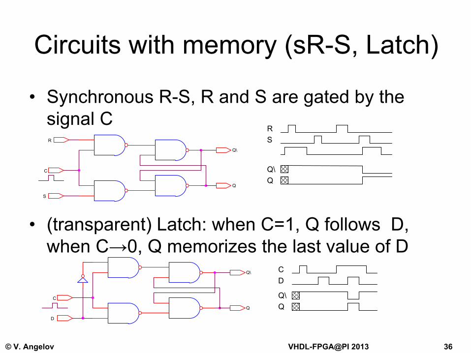
•
Synchronous R-S, R and S are gated by the signal C
•
(transparent) Latch: when C=1, Q follows D, when C→0, Q memorizes the last value of D
Circuits with memory (sR-S, Latch)
C
Q
D
Q\
S
C
Q
Q\
R
CD
Q\Q
RS
Q\Q

© V. Angelov VHDL-FPGA@PI 2013 37
Circuits with memory (JKFF, DFF)
•
Sensitive to the edge of the clock signal, in the rest of the time the outputs do not depend on the inputs
•
JKFF: similar to the synchronous R-S, but when J and K are both 1, it toggles its state
•
Consists of two synchronous R-S flip-flops (master- slave)
–
Used in counters in the past•
DFF: similar to the Latch: when C↑,
Q memorizes D
–
Currently the most used memorizing component together with the memories (RAM)
–
Some flip-flop types have an additional enable input and asynchronous set or reset inputs

© V. Angelov VHDL-FPGA@PI 2013 38
Circuits with memory (DFF)•
D must be stable tS
(setup) before and tH
(hold) after the active edge of the clock signal CLK
•
The output Q settles within some time tCO
, if the conditions are violated (tS
, tH
) the state of the flip-flop is unknown, oscillations are possible
D
CLK
?Q
tS tH
tCO
DFF
D
CK
Q

© V. Angelov VHDL-FPGA@PI 2013 39
State of a sequential circuit
According to H. Hellermann
(Digital Computer System Principles):
“The state
of a sequential circuit is a collection of state variables
whose values at
any one time contain all the information about the past necessary to account for the circuit’s future behaviour”

© V. Angelov VHDL-FPGA@PI 2013 40
State machines
.
.
.
.
.
.
.
.
.
CLK
The next state S[1..M]i+1
is a function of the present S[1..M]i
and of the inputs I[1..N]. The outputs Y[1..K] are function of the present state S[1..M]i
, but could depend on the inputs I[1..N]
I1I2
IN
Y1Y2
YK
S1
S2
SM
Moore machine: the outputs depend only on the state
Mealy machine: the outputs depend on the state and on the inputs

© V. Angelov VHDL-FPGA@PI 2013 41
State machine example
The description of a state machine is often done by state diagrams. Here are shown all the states, the transitions with their conditions and the outputs. For convenience the condition to stay in the same state
can be
omitted. The conditions to exit any state should be never in conflict!
Outputs (Moore machine)Inputs State
S0
SL
SA
SR
LL LR
1 X 0 0 0
0 11 0
1 1
X X X
0 X X
0 1 X
X X 1
1 X X
X 0 X1 1 X
0 1 0
L R W
0 0 0

© V. Angelov VHDL-FPGA@PI 2013 42
.
.
.
.
.
.
.
.
.
.
.
.
.
.
.
.
.
.
CLK
Synchronous circuits
At each rising clock edge the registers memorize the current values at their inputs. The outputs are updated after some small delay tCO
T=tH
+tL
tH tL
Clock signal
register
© V. Angelov VHDL-FPGA@PI 2013 43
Register Transfer Level (RTL)
•
A digital synchronous circuit consists of registers and combinational logic between them
•
The description of such a circuit actually specifies what happens after each clock cycle –
the data transfer between the
registers –
RTL

© V. Angelov VHDL-FPGA@PI 2013 44
Structural approach: top-down
U1
U2
A
B
C
Y1
Y2
A
B
A
B
Y
Y
my_top •
Try to understand the problem, do not stop at the first most obvious solution•
Divide into subdesigns
(3..8), with
possibly less connections between them, prepare block diagrams before starting with the implementation•
Clearly define the function of each
block and the interface between the blocks, independently on the implementation(s) of each block•
Develop the blocks (in team) and
then check the functionality•
Combine all blocks into the top
module, if some of them is not finished, put temporarily
a dummy
Iterative process !•
Don't delay the documentation, it is
part of each design phase

© V. Angelov VHDL-FPGA@PI 2013 45
Structural approach: top-down• Think about compatibility and extensibility of the design•
Try to do the functionality of the module symmetrical and include all simple
and reasonable extensions•
Maximize orthogonality, do not implement functions, just because they are
"nice", but are combinations of already implemented functions (example: many ways to clear or increment some CPU register). An architecture with high orthogonality
tends to provide more function at the same level of
complexity and cost•
The hardware should be not damageable by the user, think about auto-
consistency of the configuration and about protections•
Do not spread the important constants like dimensions, addresses etc. in
the several sources of the design, put them into one central place• Try to be technologically independent as long as possible• Make the configuration registers read/write instead of write only• Think about testing and debugging

© V. Angelov VHDL-FPGA@PI 2013 46
Hardware : software?
U1
μC, RISC
A
B
C
Y1
Y2
A
B
I/O
I/O
Y
I/O
my_top
• select the processor core•
for the architecture of the
hardware
part proceed as described before
again: inc r5load r2, [r5]and r2, 0xABbra cc_zero, againstore [r3], r6...HW
SW
Just a few questions more:
•
Divide in two parts -
hardware : software, taking into account the desired speed, size, flexibility, power consumption and other conditions

© V. Angelov VHDL-FPGA@PI 2013 47
Questions, questions...
•
How to partition the design? Where to put the boundary between software and hardware?
•
How to enter the design?•
How to check whether each subblock
works as
expected, according to the description?•
How to select the possible implementation in a silicon chip?
•
How to check whether the chip will work so as we want before ordering it?
•
How to check the chip functionality when we get it back?•
How to test the chips in the production (and the boards after assembly)?

© V. Angelov VHDL-FPGA@PI 2013 48
Technologies

© V. Angelov VHDL-FPGA@PI 2013 49
Technologies•
Small Scale Integration (SSI) ICs (74xx, 4000)
•
Simple Programmable Logic Devices (SPLD) -
PAL (Programmable Array Logic) & GAL (Generic Array Logic), Complex Programmable Logic Devices (CPLD)–
Architecture, manufacturers, overview of the available products
•
Field Programmable Gate Arrays (FPGA)–
Architecture, manufacturers, overview of the available products
•
Design flow FPGA/CPLD•
Application Specific Integrated Circuit (ASIC)–
Standard cell (structured ASIC)
–
Others (gate array, full-custom)–
Design flow

© V. Angelov VHDL-FPGA@PI 2013 50
1 213
GND
7
14
6
12
9
VCC
3
10
4 5
11
8
TTL (transistor-transistor logic)•
7400 -
4 х
(4 bipolar transistors + 4 resistors)
•
74хх
–
many combinations of different logical elements (AND, OR, NOT), flip-flops, counters and many others.
•
From the modern point of view –
slow, hungry (for electrical power) monster
•
Small Scale IntegrationIC (SSI)

© V. Angelov VHDL-FPGA@PI 2013 51
TTL families•
The basic family was replaced by the LS
(Low-
power Shottky)•
Other popular subfamilies: AS
(Advanced Shottky), ALS (Advanced Low-power
Shottky) and F
(Fast)•
The industry standard for long time, used in mini computers and other digital devices
74151
4321
15141312
1110
97
6
5D0D1D2D3D4D5D6D7
ABCG
W
Y
74LS283
53
1412
62
1511
7
411310
9
A1A2A3A4
B1B2B3B4
C0
S1S2S3S4
C4
1/4 of 7402
2
31
1/4 of 7400
1
23
74LS161
3456
710291
1413121115
ABCD
ENPENTCLKLOADCLR
QAQBQCQD
RCO
1/4 of 7408
1
23
1/4 of 7432
1
23
1/2 of 747314
1
3
12
13
2
J
CLK
K
Q
QCL
1/2 of 7474
2
3
5
6
41
D
CLK
Q
Q
PR
CL
74LS174
346
111314
91
257101215
D1D2D3D4D5D6
CLKCLR
Q1Q2Q3Q4Q5Q6
1/6 of 7414
1 2
1/4 of 74125
2 3
1
1/4 of 7486
1
23
1/2 of 7420
12
45
6

© V. Angelov VHDL-FPGA@PI 2013 52
CMOS technology•
Built with nMOS
and pMOS
transistors
S
Y
S
D
NMOS
DVSS
NMOS
PMOS
Y
VDD
VDD
VSS
Y
VDD
AA=1A
VSS
A=0
PMOSG
G
Y
VDD
Y
VSS
VDD
Y Y
BA
VSS
YA=1
B
VDD
B=1
A=1
VDD
VSS
B=0
A=0
B=0
A
VSS
Y
© V. Angelov VHDL-FPGA@PI 2013 53
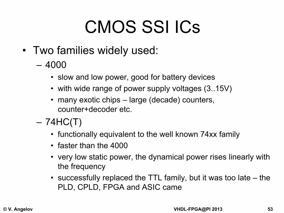
CMOS SSI ICs•
Two families widely used:–
4000
•
slow and low power, good for battery devices•
with wide range of power supply voltages (3..15V)
•
many exotic chips –
large (decade) counters, counter+decoder
etc.
–
74HC(T)•
functionally equivalent to the well known 74xx family
•
faster than the 4000•
very low static power, the dynamical power rises linearly with the frequency
•
successfully replaced the TTL family, but it was too late –
the PLD, CPLD, FPGA and ASIC came

© V. Angelov VHDL-FPGA@PI 2013 54
Simple PLD – GAL (generic array logic) 1
2
3
4
5
16
17
18
0000
0224
0256
0480
0512
0736
0768
0992
19
XOR-2048AC1-2120
XOR-2049AC1-2121
XOR-2050AC1-2122
XOR-2051AC1-2123
2824201612840 PTD2128
OLMC
OLMC
OLMC
OLMC
Programmable AND array
Output Logic Macrocells
Inpu
ts
CLK
8 PTs/OLMC
pin #
© V. Angelov VHDL-FPGA@PI 2013 55
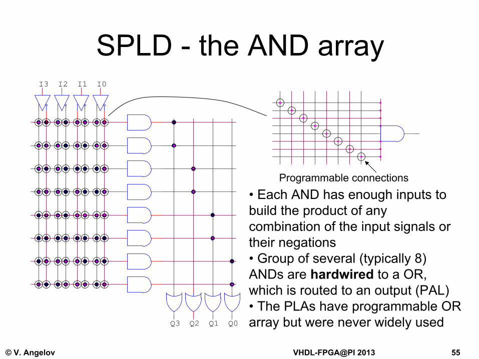
SPLD - the AND array
Programmable connections•
Each AND has enough inputs to
build the product of any combination of the input signals or their negations•
Group of several (typically 8)
ANDs
are hardwired
to a OR, which is routed to an output (PAL)•
The PLAs
have programmable OR
array but were never widely used
I2 I1
Q3
I0
Q2 Q1
I3
Q0

© V. Angelov VHDL-FPGA@PI 2013 56
GAL – Output Logic Macrocell
•
The polarity is programmable, sometimes it is easier to calculate the negation of the output signal
•
The output can be fed back to the programmable AND array
•
The chip output can be put into tri-state
• Optional register
From
/to th
e A
ND
mat
rix
0/1
0/1
From
/to th
e A
ND
mat
rix
D
CLK
Q
Q
OECLK

© V. Angelov VHDL-FPGA@PI 2013 57
PAL/GAL – summary• The first widely used programmable logic devices•
Used in the past to replace several small scale integration ICs,
like 74xx• Very successfully used for small state machines•
Manufactured first by MMI (Monolitic
Memories Inc.), later by
AMD, Lattice and others•
The first devices were one time programmable (OTP) and with
either combinational or registered macrocells
(or a fixed mixture), the later were electrically erasable/programmable (up to 100 times) with freely programmable type of the macrocells•
Software tools –
based on Hardware Description Languages
(HDL) –
ABEL, CUPL, PALASM or schematics•
The next generation of PLD –
Complex PLD (CPLD) are based on
the same architecture

© V. Angelov VHDL-FPGA@PI 2013 58
CPLD –
ispMACH
4000 (Lattice)
Output Routing Pool
CLK0..3pwr/gnd GOE0/1 JTAGpwr/gnd pwr/gnd
Global
Routing
Pool
Similar to a GAL

© V. Angelov VHDL-FPGA@PI 2013 59
CPLD – ispMACH 4000 - GLB
36 inputs from GRP
Generic Logic Block
cluster
n−1 n−2 n−1 n−4
ton+1
n+2 n+1
ton+4
Fast 5−PTPath
toXOR
(MC)
Individual PTAllocator
Cluster Allocator
n
from
fromto
shared clock, oe, reset
PTCluster 0
PTCluster 15
inputs
AND array programmable fuse
83 PTs
x16

© V. Angelov VHDL-FPGA@PI 2013 60
power upinit
sharedPT init
PT init
PT init/CE
From LogicAllocator
Single PT
delay
R P
D/T/L
CE
From I/O Cell
ORP
GRP
To
CLK0..3
PT clock
SharedPT clock
CPLD –
ispMACH
4000 Macrocell
The FF can be configured as DFF, TFF, Latch, with optional asynchronous set/reset
The output of the cell can be routed to some I/O cell via the Output Routing Pool and/or to other cells via the Global Routing Pool
Up to 80 PTs
are possible, by using the PTs
of the
neighbour cells (cluster allocator).
set/reset logic
Clock source selection

© V. Angelov VHDL-FPGA@PI 2013 61
CPLD –
ispMACH
4000 I/O-
cell
GOE0..3
From ORP
VCC
From ORP
To Macrocell
To GRP
Globalfuses
Vcco
bus keeper pull−up
pull−down
The output cell can be configured as input, output or bidirectional. Weak pull-up/down resistors and bus keepers are globally available.
Output enable selection
outputinput
with
tri-s
tate
From Output Routing Pool
To MacrocellTo Global Routing Pool
I/O pin
© V. Angelov VHDL-FPGA@PI 2013 62
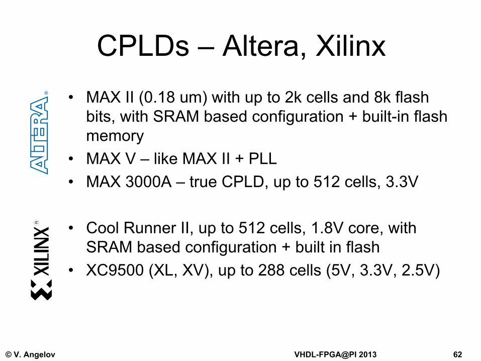
CPLDs – Altera, Xilinx•
MAX II (0.18 um) with up to 2k cells and 8k flash bits, with SRAM based configuration + built-in flash memory
•
MAX V –
like MAX II + PLL•
MAX 3000A –
true CPLD, up to 512 cells, 3.3V
•
Cool Runner II, up to 512 cells, 1.8V core, with SRAM based configuration + built in flash
•
XC9500 (XL, XV), up to 288 cells (5V, 3.3V, 2.5V)
R

© V. Angelov VHDL-FPGA@PI 2013 63
CPLDs – Lattice•
ispMACH
4000 Z-ZE (zero power 1.8V
core), C, B, V (1.8, 2.5, 3.3V core), up to 512 cells, probably the fastest
true CPLD
now•
MachXO, 1.2, 1.8, 2.5, 3.3V core, up to 2k cells (LUT4), RAM, with SRAM based configuration + built in flash memory
•
MachXO2 –
same as MachXO
+ up to 7k cells (LUT4), PLL, hardcores
I2C, SPI, user
flash memory

© V. Angelov VHDL-FPGA@PI 2013 64
CPLD – summarySum of product terms architecture, similar to PAL/GAL
•
Simple model of the internal delays and from pin to pin•
Ready to operate immediately after power up
•
In situ programmable using JTAG, FLASH memory cells store the configuration (about 10,000 times)
•
Reliable copy protection possible•
Radiation tolerant (the newer CPLDs
are similar to
FPGA + built-in FLASH and are NOT radiation tolerant!)•
Limited number of logic elements (up to about 1k)
•
Higher price/logic element•
No internal RAM

© V. Angelov VHDL-FPGA@PI 2013 65
FPGA – general structure
Logic Block (LE, LC, Slice)
I/O Blocks and pins
-
contains a look up table (LUT) with 4 to 6 inputs and a FF. In some FPGAs
several
Logic Blocks are grouped into clusters with some local routing.
Routing channels-
general purpose
-
for global signals like clocks, reset, output enable, with high fanout
and low skew
2
3
5
1
D
CLK
Q
CL
2
3
5
1
D
CLK
Q
CL
2
3
5
1
D
CLK
Q
CL
2
3
5
1
D
CLK
Q
CL
2
3
5
1
D
CLK
Q
CL
2
3
5
1
D
CLK
Q
CL
2
3
5
1
D
CLK
Q
CL
2
3
5
1
D
CLK
Q
CL
2
3
5
1
D
CLK
Q
CL
2
3
5
1
D
CLK
Q
CL
2
3
5
1
D
CLK
Q
CL
2
3
5
1
D
CLK
Q
CL
2
3
5
1
D
CLK
Q
CL
2
3
5
1
D
CLK
Q
CL
2
3
5
1
D
CLK
Q
CL
2
3
5
1
D
CLK
Q
CL

© V. Angelov VHDL-FPGA@PI 2013 66
FPGA – Virtex 4 SLICE L/M
LUT
FX
Ginputs
FXINA MUXFX
FXINB
DFF/LAT
Q
REV
D
CE
CLK
SR
BY
BX
CE
CLK
SR
Y
YQ
F5MUXF5
XLUT
Finputs
D
FF/LAT
Q
REV
D
CE
CLK
SR
XQ
UG070_5_20_071504
Each SLICE contains two LUT4, two FFs
and
MUXes. The two LUT4 can be combined into one LUT5.
The Configurable Logic Block (CLB) contains 2x SLICEL and 2x SLICEM. The Ms can be used for distributed RAM and large shift registers.
The CLB has 8 LUT4, 8 FFs, can be used for 64 bits distributed RAM or shift register

© V. Angelov VHDL-FPGA@PI 2013 67
FPGA – Virtex 5 with LUT6
WP284_01_121907
B
BQ
BMUX
6-Input LUTB6
BX
B5B4B3B2B1
COUT
CIN
In the modern sub-micron processes the routing delay becomes a substantial part of the whole delay. On the other side the logic
needs
less area. Therefore the leading manufacturers go to larger LUT6.
Can operate as 1 LUT6 or 2 LUT5 with common inputs
x4 → SLICE, 2 x SLICEs
→ CLB
The CLB contains 8 LUT6, 8 FFs; can be used as distributed RAM with 256 bits or as a 128 bit shift register
© V. Angelov VHDL-FPGA@PI 2013 68
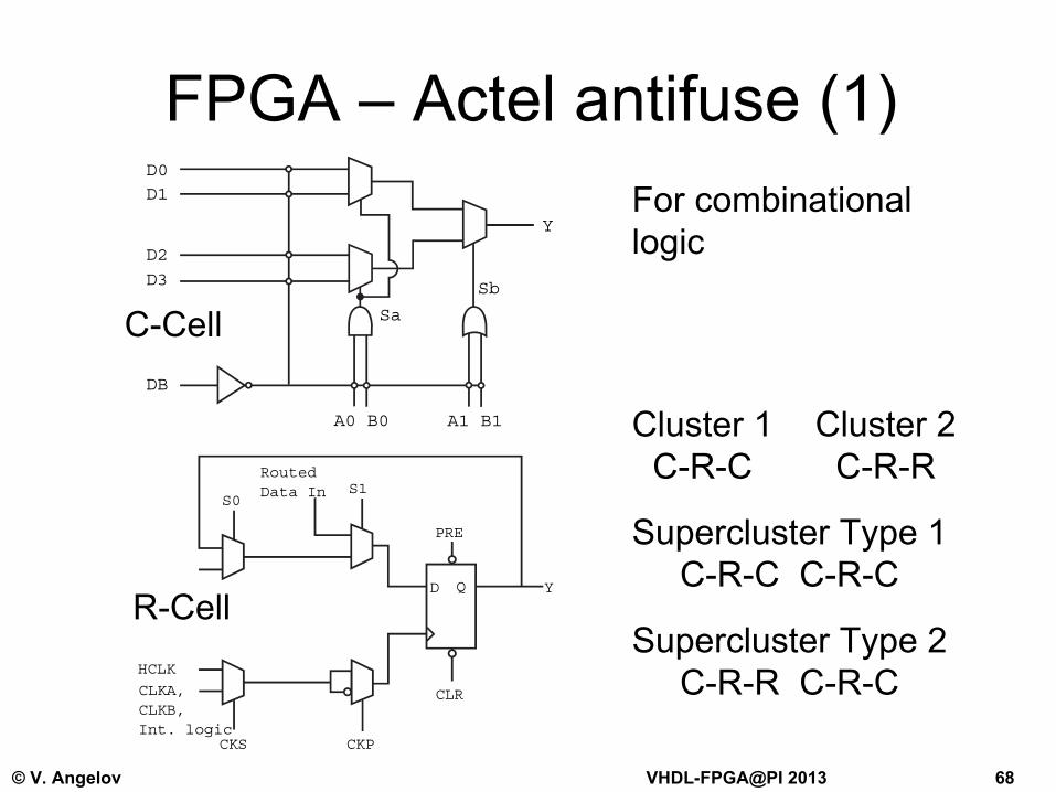
D0D1
D2
D3
DB
A0 B0 A1 B1
Sa
Sb
Y
FPGA – Actel antifuse (1)
C-Cell
Cluster 1C-R-C
For combinational logic
R-Cell
Supercluster
Type 1C-R-C C-R-C
Cluster 2C-R-R
Supercluster
Type 2C-R-R C-R-C
S0S1
RoutedData In
D
PRE
CLR
Q Y
CKPCKS
HCLK
CLKA,CLKB,Int. logic

© V. Angelov VHDL-FPGA@PI 2013 69
FPGA – Actel antifuse (2)
The same for the FLASH FPGAs
of
Actel
•
Don‘t need configuration memory, lower price, more reliable
•
Illegal copy is impossible•
Radiation tolerant
•
Perfect prototyping service
•
Every chip is exactly once programmable
•
Design flow similar to ASIC•
Slightly slower

© V. Angelov VHDL-FPGA@PI 2013 70
Low cost FPGAs overview
Name
LUT4 (k)
RAM kBits
18x18
PLLs
TechCyclone II
4-68
120-1100
13-150
2-4
90nm
Cyclone III
5-120
400-3800 23-288
2-4
65nm (lp)
Cyclone IV E
14-150
270-3800 15-266
2-4
60nm (lp)
Cyclone V E
25-301
1760-12200
50-684
4-8
28nm (lp)
Name
LUT4 (k)
RAM kBits
18x18
DLLs
TechSpartan 3
2-75
72-1800
4-104
2-4
90nm
Spartan 3E
2-33
72-650
4-36
2-8
90nmSpartan 3A/AN
2-25
54-576
3-32
2-8
90nm
Spartan 3D
37-53
1500-3200
84-126
8 90nm
Spartan 6 3-147
216-4800
8-180
4PLL
45nm
Artix-7
16-71
208-974 60-250
4PLL
28nm
R
with built-in flash equivalent
LUT4, but LUT6

© V. Angelov VHDL-FPGA@PI 2013 71
Low cost FPGAs overview
Name
LUT4 (k)
RAM kBits
18x18
PLLs
TechLatticeXP
3-20
54-396
---
2-4
130nmLatticeXP2
5-40
166-885
12-32
2-4
90nm
XP and XP2 have built-in configuration flash
Name LUT4 (k)
RAM kBits 18x18 SerDes Speed
GbpsTech
Cyclone
IV GX 14-150 540-6400 0-360 2-8 3.125 60nm
Cyclone
V GX/T 77-301 4460-12200 300-684 2-12 6.144 28nm
Spartan
6 24-147 936-4824 38-180 2-8 3.125 45nm
Artix-7 16-215 208-2888 60-740 4-16 6.6 28nmwith
Ser
Des
© V. Angelov VHDL-FPGA@PI 2013 72
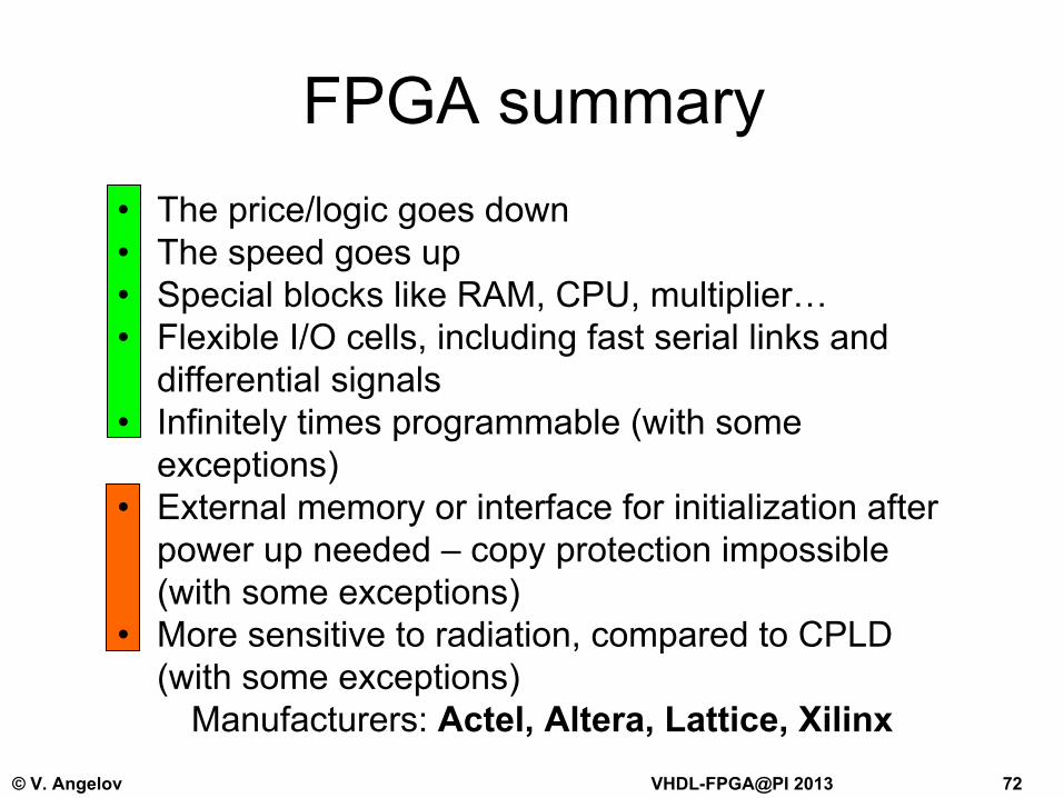
FPGA summary•
The price/logic goes down
•
The speed goes up•
Special blocks like RAM, CPU, multiplier…
•
Flexible I/O cells, including fast serial links and differential signals
•
Infinitely times programmable (with some exceptions)
•
External memory or interface for initialization after power up needed –
copy protection impossible
(with some exceptions)•
More sensitive to radiation, compared to CPLD (with some exceptions)
Manufacturers: Actel, Altera, Lattice, Xilinx

© V. Angelov VHDL-FPGA@PI 2013 73
Design flow CPLD/FPGA
Your favourite text editor!Some recommendations: emacs, notepad++, nedit, with syntax colouring and more for VHDL
and Verilog
LeoSpecPrecisionSynplify
FPGA vendorsSynopsys
ModelSimAldec AHDL
FPGA vendor
Device programming
Each step can take seconds, minutes, hours ... (place & route)
functional simulation
synthesis
timing estimation
gate-level simulation
place & route
sdf
simulation
timing analysis
design entry: schematic, HDL
board production
& test

© V. Angelov VHDL-FPGA@PI 2013 74
FPGA development tools•
Each manufacturer has own tools, absolutely necessary for placing and routing, optionally for synthesis, simulation etc. The free versions have some limitations
•
Leading suppliers of synthesis tools -
Mentor Graphics (Leonardo Spectrum, Precision), Synopsys (FPGA compiler), Synplicity
(Synplify) –
already part of Synopsys
•
Leading suppliers of simulation tools -
Mentor Graphics (ModelSim), Aldec
(Active HDL)
•
The FPGA manufacturers offer free but limited versions of the synthesis and simulation tools mentioned above

© V. Angelov VHDL-FPGA@PI 2013 75
ASICs - Standard Cells, Gate Arrays, Full Custom
•
Standard Cells–
rich library with primitive functions and flip-flops
–
I/O cells for different standards and voltages–
core generators for memory, CPU, interfacing, PLL
–
the user must pay all production masks–
multiproject
wafer option for prototyping
•
Gate Array–
array of ready simple gates
–
the user prepares only some routing masks–
compared to Standard Cells: cheaper, slower, no mixed mode
•
Full custom –
for very high volumes–
the most optimal, even longer development time and higher costs

© V. Angelov VHDL-FPGA@PI 2013 76
ASIC ↔ FPGA•
ASICs
compared to CPLD and FPGAs:
–
lower price in high volume production runs–
possibility for mixed mode designs (with analog
part)
–
higher design density, higher operation speed, lower power–
much longer development time, several months per submission
–
higher development costs and much more expensive software
•
FPGA to ASIC–
FPGA architecture, with fixed routing and function of each cell
–
compared to FPGA•
cheaper for mid-volume production and large designs
•
faster & smaller chips, lower power, no configuration memories•
radiation tolerant
–
Altera
HardCopy, eASIC

© V. Angelov VHDL-FPGA@PI 2013 77
Design flow ASIC
Synopsys
ModelSim
CadenceFirst
Encountersubmission
DRC, LvS
The process can take months!The manufacturing too!Price for ≈100 prototypes ≈$10,000
functional simulation
synthesis
timing estimation
gate-level simulation
place & route
sdf
simulation
timing analysisdesign entry:
schematic, HDL
production
wafer test
packaging & test
board production
& test
Calibre
PrimeTime
Your favour text editor!Some recomendations: emacs, notepad++, nedit, with syntax coloring
and more for VHDL
and Verilog