Introduction Key Features Specifications - renesas.com · many shared features such as clock...
15
USER’S MANUAL UG014 Rev 0.00 December 18, 2014 ZL6105-1CH-DEMO1Z Demonstration Board User Guide UG014 Rev 0.00 Page 1 of 15 December 18, 2014 Introduction The ZL6105 is an innovative power conversion and management IC that combines integrated MOSFET drivers with key power and fault management functions in a small package, resulting in a flexible and integrated solution. The ZL6105-1CH-DEMO1Z platform allows quick evaluation of the highly configurable ZL6105’s performance and features in either stand-alone mode or via the SMBus™ interface using Intersil’s PowerNavigator™ GUI software. Specifications This board has been configured and optimized for the following range of operating conditions: •V IN = 5.5V to 14V •V OUT = 0.6V to 3.6V •I MAX = 40A •f SW = 300kHz to 1333kHz • Peak efficiency: >90% at 50% load • Output ripple: <1% at 50% load Key Features • Optimized for small circuit footprint • Onboard enable switch • Power-good indicator • SMBus control interface • Interconnectivity with other Intersil demo boards References • ZL6105 , Datasheet • AN2010 , “Thermal and Layout Guidelines for Digital-DC TM Products” • AN2035 , “Compensation Using CompZL TM ” • AN1779 , “Configuring Current Sharing on the ZL6105 and ZL8101” • TB389 , “PCB Land Pattern and Surface Mount Guidelines for QFN Packages” Ordering Information PART NUMBER DESCRIPTION ZL6105-1CH-DEMO1Z ZL6105 Evaluation Kit, one channel (EVB, USB adapter, Cable, Software FIGURE 1. ZL6105-1CH-DEMO1Z SIMPLIFIED SCHEMATIC ZL6105 V IN DDC SMBus V OUT EN SYNC ENABLE SW1 ENABLE SYNC SMBus DDC ENABLE SYNC SMBus DDC
Transcript of Introduction Key Features Specifications - renesas.com · many shared features such as clock...

USER’S MANUAL
UG014Rev 0.00
December 18, 2014
ZL6105-1CH-DEMO1ZDemonstration Board User Guide
IntroductionThe ZL6105 is an innovative power conversion and management IC that combines integrated MOSFET drivers with key power and fault management functions in a small package, resulting in a flexible and integrated solution. The ZL6105-1CH-DEMO1Z platform allows quick evaluation of the highly configurable ZL6105’s performance and features in either stand-alone mode or via the SMBus™ interface using Intersil’s PowerNavigator™ GUI software.
SpecificationsThis board has been configured and optimized for the following range of operating conditions:
• VIN = 5.5V to 14V
• VOUT = 0.6V to 3.6V
• IMAX = 40A
• fSW = 300kHz to 1333kHz
• Peak efficiency: >90% at 50% load
• Output ripple: <1% at 50% load
Key Features• Optimized for small circuit footprint
• Onboard enable switch
• Power-good indicator
• SMBus control interface
• Interconnectivity with other Intersil demo boards
References• ZL6105, Datasheet
• AN2010, “Thermal and Layout Guidelines for Digital-DCTM Products”
• AN2035, “Compensation Using CompZLTM”
• AN1779, “Configuring Current Sharing on the ZL6105 and ZL8101”
• TB389, “PCB Land Pattern and Surface Mount Guidelines for QFN Packages”
Ordering InformationPART NUMBER DESCRIPTION
ZL6105-1CH-DEMO1Z ZL6105 Evaluation Kit, one channel (EVB, USB adapter, Cable, Software
FIGURE 1. ZL6105-1CH-DEMO1Z SIMPLIFIED SCHEMATIC
ZL6105
VIN
DDCSMBus
VOUT
ENSYNC
ENABLE
SW1
ENABLESYNC
SMBusDDC
ENABLESYNCSMBusDDC
UG014 Rev 0.00 Page 1 of 15December 18, 2014

ZL6105-1CH-DEMO1Z
ZL6105-1CH-DEMO1Z BOARD
FIGURE 2. TOP SIDE
FIGURE 3. BOTTOM SIDE
UG014 Rev 0.00 Page 2 of 15December 18, 2014
ZL6105-1CH-DEMO1Z
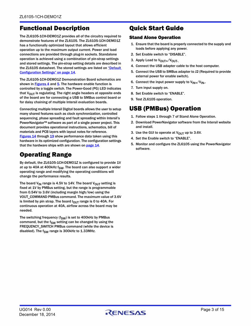
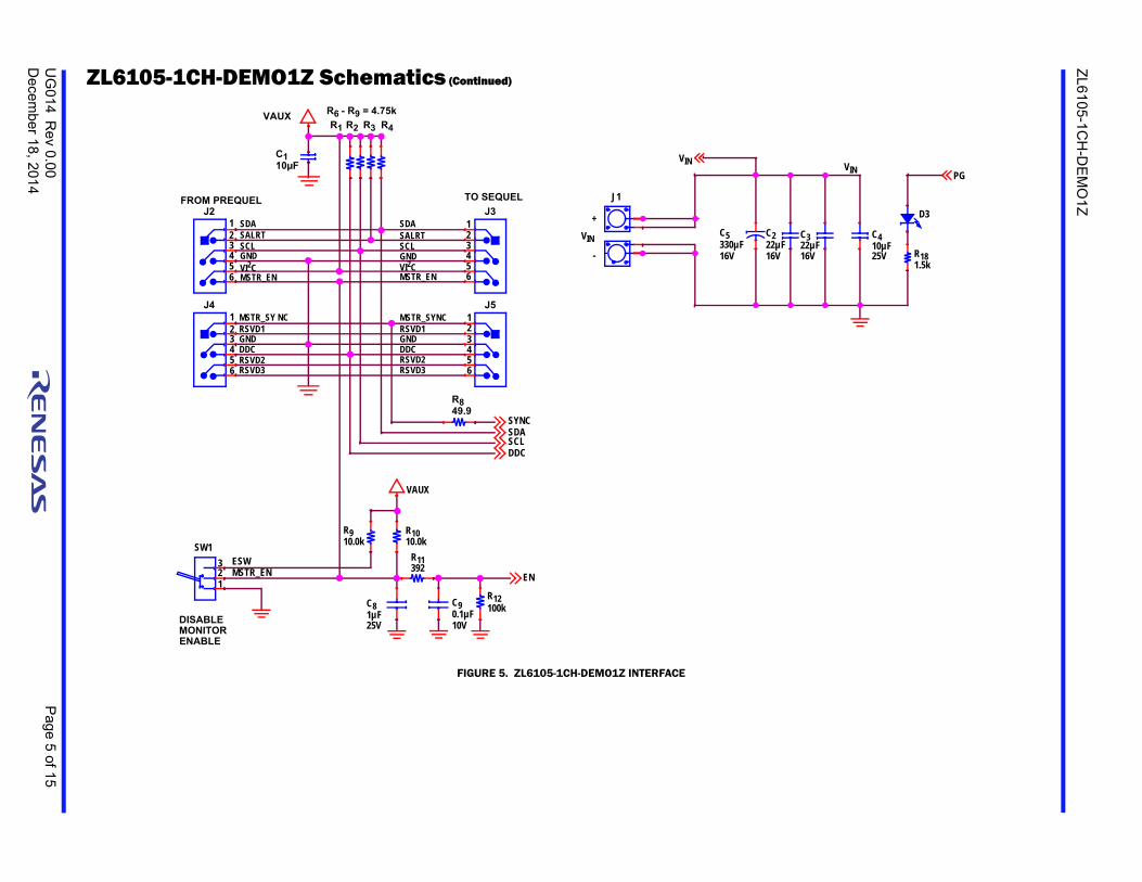
Functional DescriptionThe ZL6105-1CH-DEMO1Z provides all of the circuitry required to demonstrate features of the ZL6105. The ZL6105-1CH-DEMO1Z has a functionally optimized layout that allows efficient operation up to the maximum output current. Power and load connections are provided through plug-in sockets. Standalone operation is achieved using a combination of pin-strap settings and stored settings. The pin-strap setting details are described in the ZL6105 datasheet. The stored settings are listed on “Default Configuration Settings” on page 14.
The ZL6105-1CH-DEMO1Z Demonstration Board schematics are shown in Figures 4 and 5. The hardware enable function is controlled by a toggle switch. The Power-Good (PG) LED indicates that VOUT is regulating. The right angle headers at opposite ends of the board are for connecting a USB to SMBus control board or for daisy chaining of multiple Intersil evaluation boards.
Connecting multiple Intersil Digital boards allows the user to setup many shared features such as clock synchronization, controlled sequencing, phase spreading and fault spreading within Intersil’s PowerNavigator™ software as part of a single power project. This document provides operational instructions, schematics, bill of materials and PCB layers with layout notes for reference. Figures 14 through 19 show performance data taken using this hardware in its optimized configuration. The configuration settings that the hardware ships with are shown on page 14.
Operating RangeBy default, the ZL6105-1CH-DEMO1Z is configured to provide 1V at up to 40A at 400kHz fSW. The board can also support a wider operating range and modifying the operating conditions will change the performance results.
The board VIN range is 4.5V to 14V. The board VOUT setting is fixed at 1V by PMBus setting, but the range is programmable from 0.54V to 3.6V (including margin high/low) using the VOUT_COMMAND PMBus command. The maximum value of 3.6V is limited by pin strap. The board IOUT range is 0 to 40A. For continuous operation at 40A, airflow across the board may be needed.
The switching frequency (fSW) is set to 400kHz by PMBus command, but the fSW setting can be changed by using the FREQUENCY_SWITCH PMBus command (while the device is disabled). The fSW range is 300kHz to 1.33MHz.
Quick Start GuideStand Alone Operation1. Ensure that the board is properly connected to the supply and
loads before applying any power.
2. Set Enable switch to “DISABLE”.
3. Apply Load to VOUT+/VOUT-.
4. Connect the USB adapter cable to the host computer.
5. Connect the USB to SMBus adapter to J2 (Required to provide external power for enable switch).
6. Connect the input power supply to VIN+/VIN-.
7. Turn input supply on.
8. Set Enable switch to “ENABLE”.
9. Test ZL6105 operation.
USB (PMBus) Operation1. Follow steps 1 through 7 of Stand Alone Operation.
2. Download PowerNavigator software from the Intersil website and install.
3. Use the GUI to operate at VOUT up to 3.6V.
4. Set the Enable switch to “ENABLE”.
5. Monitor and configure the ZL6105 using the PowerNavigator software.
UG014 Rev 0.00 Page 3 of 15December 18, 2014

UG
014R
ev 0.00P
age 4 of 1
5D
ece
mb
er 1
8, 2
014
ZL
610
5-1CH
-DE
MO
1Z
VOUT
+
VOUT
-
J7
VOUT1
J8
1
C211500µF4V
FC18100µF6.3V
C19100µF6.3V
C20100µF6.3V
ZL6105-1CH-DEMO1Z Schematics
FIGURE 4. ZL6105-1CH-DEMO1Z DEMO BOARD
SENA
VR
R1761.9k
SDASCL
DDCPG
XX1
VIN
GL
XX2EN
SYNCSYNC
R16100k
EN
R131
XX4
VIN VDD
XX5
SW
L1470nH
Address = Ox16
U2ZL6105-02
DGND 1
SYNC2
SA03
SA14
CFG06
SCL7
SDA8
SALRT9
FC010
FC111
V012
V113
SS15
VTRK16
VSEN+17
VSEN- 18
ISENB 19ISENA
20GL
22
PGND23
GH25
BST 26
21VR
VDD27
V2528
XTEMP29
DDC30
MGN31
EN33
PH_EN34
CFG235
PG36
ILIM5
UVLO14
SW24
CFG132
SGND37
SDA
SG
PG
C2210µF6.3V
C1310µF
C141µF16V
D4BAT54
C151µF16V
C1022µF16V
SENB
C16100µF6.3V
FB+
SCL
Q2BSC050NE2LS5
C1122µF16V
C1222µF16V
Q3BSC010NE2LS
GH
C17100µ6.3V
R14698
XX3
R15100k
C2310µF6.3V
DDC
R19 3.48k
UG
014R
ev 0.00P
age 5 of 1
5D
ece
mb
er 1
8, 2
014
ZL
610
5-1CH
-DE
MO
1Z
VIN
C410µF25V R18
1.5k
D3
PG
FIGURE 5. ZL6105-1CH-DEMO1Z INTERFACE
ZL6105-1CH-DEMO1Z Schematics (Continued)
R2 R3R1
EN
VI2C
RSVD1 RSVD1
SCL
RSVD3 RSVD3RSVD2 RSVD2
GND
C110µF
J2
2
4
6
1
3
5
J4
2
4
6
1
3
5
GND
J3
2
4
6
1
3
5GND
SDASALRT
J5
2
4
6
1
3
5DDC
MSTR_EN
MSTR_SYNC
VAUX
SALRT
TO SEQUEL
SCL
SDA
GNDVI2C
DDC
MSTR_SY NC
MSTR_EN
SCL
R910.0k
R1010.0k
SYNC
DDC
DISABLE
R849.9
C81µF25V
C90.1µF10V
R11392
VAUX
SW1
123 ESW
R12
R4
MSTR_EN
R6 - R9 = 4.75k
SDA
C5330µF16V
C222µF16V
C322µF16V
+
VIN
-
VIN
J1
100k
MONITORENABLE
FROM PREQUEL
-

ZL6105-1CH-DEMO1Z
Bill of Materials
QTY REFERENCE VALUETOL(%) RATING TYPE PCB FOOTPRINT MANUFACTURER PART NUMBER
1 U2 ZL6105 MLF36_6X6BX Intersil Corporation
2 C2, C3 22µF 20 16V X5R SM1206 Murata GRM31CR61C226ME15L
1 C4 10µF 10 25V X5R SM1206 Panasonic - ECG ECJ-3YB1E106K
1 C5 330µ 20 16V AL POLY SM_CAP_10.5X10.5_PXA_FLD
United Chemi-Con APXA160ARA331MJC0G
1 C8 1µF 10 25V X5R SM0603 Taiyo Yuden TMK107BJ105KA-T
1 C9 0.1µF 10 10V X7R SM0603 Kemet C0603C104K8RACTU
3 C10, C11, C12
22µF 20 16V X5R SM1206 Panasonic - ECG ECJ-3YB1C226M
1 C13 10µF 10 25V X7R SM1206 Taiyo Yuden TMK316B7106KL-TD
2 C14, C15 1µF 10 16V X7R SM0603 AVX Corporation 0603YC105KAT2A
5 C16, C17, C18, C19,
C20
100µF 20 6.3V X5R SM1206 TDK Corporation C3216X5R0J107M
1 C21 1500µF 20 4V AL POLY SM7343_KEMET_T530_BC
AVX TPME158K004R0018
2 C22, C23 10µF 10 6.3V X7R SM0805 TDK Corporation CGA4J1X7R0J106K125AC
1 D4 BAT54 30V Schottky SOD_523 ON Semiconductor BAT54XV2T1OS
1 L1 470nH 0.8mΩ Inductor IND_HCM1305_XX Cooper Bussmann HCM1305-R47-R
1 Q2 BSC050NE2LS5 30V PG_TDSON_8_LAS Infineon
1 Q3 BSC010NE2LS 30V PG_TDSON_8_LAS Infineon
4 R1, R2, R3, R4
4.75k 1 1/16W SM0402 Panasonic - ECG ERJ-2RKF4751X
1 R13 1 1 1/16W SM0603 Panasonic - ECG ERJ-3RQF1R0V
1 R14 953 1 1/16W SM0603 Panasonic ERJ-3EKF9530V
2 R15, R16 100k 1 1/16W SM0402 Vishay/Dale CRCW0402100KFKED
1 R17 133k 1 1/16W SM0402 Panasonic - ECG ERJ-2RKF1333X
1 R19 3.48k 1 1/16W SM0402 Panasonic - ECG ERJ-2RKF3481X
ANCILLARY PARTS SPECIFIC TO DEMO BOARD OPERATION
1 C1 10µF 10 10V X7R SM0805 Taiyo Yuden LMK212B7106KG-TD
1 D3 GRN 1.8V DIO_LG_T67K Osram LG T67K-H2K1-24-Z
2 J2, J4 HDR_3x2_RA RA HDRM3DUALRA100X100
SAMTEC TSW-103-08-T-D-RA
2 J3, J5 SKT_3x2_RA RA HDRF3DUALRA100X100 SAMTEC SSQ-103-02-T-D-RA
1 R8 49.9 1 100mW THK FILM
SM0402 PANASONIC-ECG ERJ-2RKF49R9X
2 R9, R10 10.0k 1 63mW THK FILM
SM0402 Panasonic - ECG ERJ-2RKF1002X
1 R11 392 1 100mW THK FILM
SM0402 Panasonic ERJ-2RKF3920X
1 R12 100k 1 63mW THK FILM
SM0402 Panasonic - ECG ERJ-2RKF1003X
1 R18 1.5K 1 63mW THK FILM
SM0603 Panasonic - ECG ERJ-3EKF1501V
1 SW1 SW_SPDT PCB VERT
SW_TOG_ULTRAMIN_SPDT
NKK G13AP-RO
UG014 Rev 0.00 Page 6 of 15December 18, 2014

ZL6105-1CH-DEMO1Z
4 J1A, J1B, J7, J8
JACK_BANANA JACK_KEYSTONE_575-4 Keystone Electronics
575-4
4 STANDOFF_#4-40.75LG
STANDOFF_4-40_NDH
4 SCREW_#4-40.25"
SCREW_4-40
Bill of Materials (Continued)
QTY REFERENCE VALUETOL(%) RATING TYPE PCB FOOTPRINT MANUFACTURER PART NUMBER
UG014 Rev 0.00 Page 7 of 15December 18, 2014

ZL6105-1CH-DEMO1Z
Measured Data The following data was obtained using a ZL6105-1CH-DEMO1Z evaluation board. VIN = 12V for all data.
FIGURE 6. EFFICIENCY DATA AT 300kHz FIGURE 7. EFFICIENCY DATA AT 400kHz
FIGURE 8. EFFICIENCY DATA AT 500kHz FIGURE 9. EFFICIENCY DATA AT 600kHz
60
65
70
75
80
85
90
95
0 10 20 30 40
VOUT = 1.2V
VOUT = 1.8V
EF
FIC
IEN
CY
(%
)
OUTPUT CURRENT (A)
VOUT = 1V
VOUT = 1.5VVOUT = 3.3V
VOUT = 2.5V
60
65
70
75
80
85
90
95
100
0 10 20 30 40
OUTPUT CURRENT (A)
VOUT = 1V
VOUT = 1.8V
VOUT = 1.2V
EF
FIC
IEN
CY
(%
)
VOUT = 2.5V VOUT = 1.5V
VOUT = 3.3V
69
74
79
84
89
94
99
0 10 20 30 40
EF
FIC
IEN
CY
(%
)
OUTPUT CURRENT (A)
VOUT = 1V
VOUT = 2.5V
VOUT = 3.3V
VOUT = 1.2V
VOUT = 1.8V VOUT = 1.5V
60
65
70
75
80
85
90
95
100
0 10 20 30 40
VOUT = 1.8V
OUTPUT CURRENT (A)
EF
FIC
IEN
CY
(%
)
VOUT = 3.3V
VOUT = 1.0V
VOUT = 1.5V
VOUT = 2.5V
VOUT = 1.2V
UG014 Rev 0.00 Page 8 of 15December 18, 2014

ZL6105-1CH-DEMO1Z
FIGURE 10. TYPICAL TURN-ON RAMP, TRISE = 5ms, tON_DELAY = 5ms
FIGURE 11. TYPICAL TURN-OFF RAMP, tFALL = 5ms, tOFF_DELAY = 5ms
FIGURE 12. TRANSIENT RESPONSE 5 TO 15A, 5A/µ FIGURE 13. STATIC RIPPLE
Measured Data The following data was obtained using a ZL6105-1CH-DEMO1Z evaluation board. VIN = 12V for all data. (Continued)
ZL6105-1CH-DEMO1Z
VIN = 12V, VOUT = 1V
IOUT = 20A, fSW = 400kHz
tON_DELAY
5ms
ENABLE
TYPICAL RAMP ARTIFACTVOUT
ENABLEtON_DELAY
5ms
tOFF
5ms
ZL6105-1CH-DEMO1Z
VIN = 12V, VOUT = 1V
IOUT = 20A, fSW = 400kHz
VOUT
ZL6105-1CH-DEMO1Z
VIN = 12V, VOUT = 1VIOUT = 20A, fSW =400kHz
MEASURED ACROSS C21
INDUCTIVE LOAD CABLE ARTIFACT
100 mV
VOUT = 1V
ZL6105-1CH-DEMO1Z
VIN = 12V, VOUT = 1VIOUT = 20A, fSW = 400kHz
TYPICAL STATIC VOUT RIPPLE PROFILE
STATIC RIPPLE = 8mV
UG014 Rev 0.00 Page 9 of 15December 18, 2014

ZL6105-1CH-DEMO1Z
ZL6105 PCB Layout GuidelinesDevice Ground Pins
- SGND is the analog reference for VDD, VR, V25, XTEMP and the pin straps. Very little current passes through this path normally.
- DGND is the high current digital GND return path for the controller. It is isolated internally from SGND to avoid noise coupling.
- PGND is the high current GND return for the MOSFET drivers and the bootstrap circuit. It is isolated internally from SGND to avoid noise coupling.
Ground Pin Usage- The pins are isolated within the device only to avoid noise
coupling through the package and bond wires. They should be tied together on the PCB with a very low impedance connection for best operation. If the DGND pin is not closely coupled to SGND, the SGND pin will become a current path for digital circuits and will get noisy.
Device Power Supply Pins- VDD is the input supply pin. It provides power to the internal
VR regulator.
- VR is the internal 5V regulator used to power the MOSFET drivers and the V25 regulator.
- V25 is the internal 2.5V regulator used to power the digital circuits.
Power Supply Pin Usage- VDD, VR and V25 are all referenced to SGND and all need to
have capacitors placed closely to the pins.
ZL6105 Voltage, Current and Temperature Sense Connections• Ensure that the current sense signals are routed differentially
and that the averaging circuit is Kelvin connected to the sensing element for most accurate current sense.
• Ensure that the voltage sense signals are routed differentially and are Kelvin connected to the final capacitor away from the inductor for best noise performance.
• Ensure that the XTEMP and SGND traces are routed differentially to the temperature sensing transistor.
UG014 Rev 0.00 Page 10 of 15December 18, 2014

ZL6105-1CH-DEMO1Z
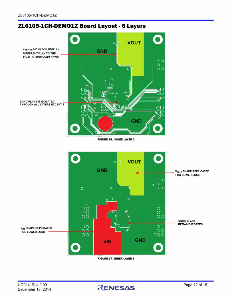
ZL6105-1CH-DEMO1Z Board Layout - 6 Layers
FIGURE 14. PCB TOP LAYER
FIGURE 15. INNER LAYER 1
Top Layer
7
PGND PIN TO COMMON GND PLANE DIRECTLY AT LS FET
VDD CAPACITOR TO COMMON GND PLANE
DGND PIN TIED TO COMMON
VIN
GND PLANE ON ALL LAYERS WITH A VIA
VOUT
TIGHT SWITCHING LOOP
COMMON GND PLANE ON
MANY GND VIAS FOR GOOD ELECTRICAL AND THERMAL PERFORMANCE
ALL LAYERS
ALL PIN STRAPS CLOSE TO DEVICE AND TIED TO INTERNALSGND PLANE
Inner layer 1
8
GNDVOUT
GND
COMPLETE GND PLANE
THROUGHOUT THIS LAYER
PROVIDES A REFERENCE
FOR ROUTED LAYERS
ISOLATED SGND PLANE
IS RECONNECTED TO
GND DIRECTLY UNDER
PGND PIN
SGND PLANE
UG014 Rev 0.00 Page 11 of 15December 18, 2014
ZL6105-1CH-DEMO1Z
FIGURE 16. INNER LAYER 2
FIGURE 17. INNER LAYER 3
ZL6105-1CH-DEMO1Z Board Layout - 6 LayersInner Layer 2
9
GNDVOUT
GND
VSENSE LINES ARE ROUTED
DIFFERENTIALLY TO THE
FINAL OUTPUT CAPACITOR
SGND PLANE IS ISOLATED THROUGH ALL LAYERS EXCEPT 1
Inner Layer 3
10
GNDVOUT
GNDVIN
VIN SHAPE REPLICATED
FOR LOWER LOSS
VOUT SHAPE REPLICATED
SGND PLANE
FOR LOWER LOSS
REMAINS ISOATED
UG014 Rev 0.00 Page 12 of 15December 18, 2014

ZL6105-1CH-DEMO1Z
FIGURE 18. INNER LAYER 4
FIGURE 19. BOTTOM LAYER
ZL6105-1CH-DEMO1Z Board Layout - 6 LayersInner Layer 4
11
GNDVOUT
GNDVIN
REPLICATION OF
INNER LAYER 3
FOR LOWER LOSS
Bottom Layer
12
GNDVOUT
GNDVIN
V25 CAPACITOR CLOSE TO THE
DEVICE AND TIED TO
SGND PLANE
VR CAPACITOR CLOSE TO THE DEVICE AND TIED TO SGND PLANE NEAR THE SGND/GND RECONNECTION POINT
ISENSE LINES ARE ROUTED
DIFFERENTIALLY AND KELVIN CONNECTED TO THE INDUCTOR
UG014 Rev 0.00 Page 13 of 15December 18, 2014
ZL6105-1CH-DEMO1Z
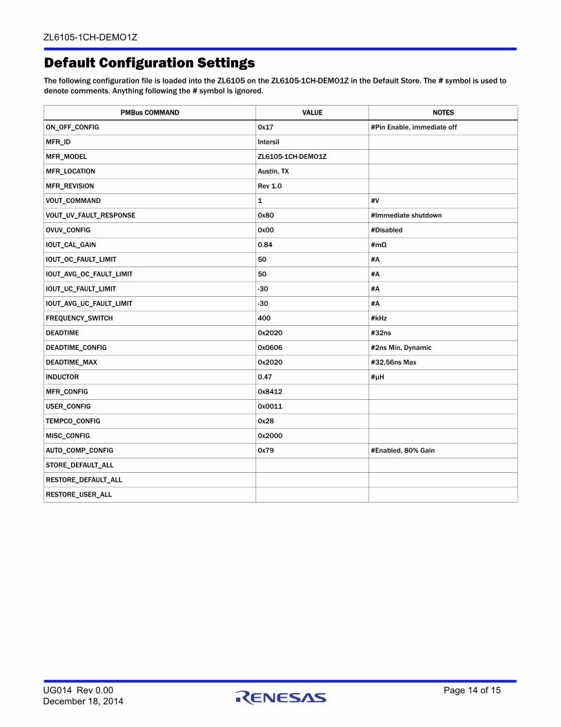
Default Configuration SettingsThe following configuration file is loaded into the ZL6105 on the ZL6105-1CH-DEMO1Z in the Default Store. The # symbol is used to denote comments. Anything following the # symbol is ignored.
PMBus COMMAND VALUE NOTES
ON_OFF_CONFIG 0x17 #Pin Enable, immediate off
MFR_ID Intersil
MFR_MODEL ZL6105-1CH-DEMO1Z
MFR_LOCATION Austin, TX
MFR_REVISION Rev 1.0
VOUT_COMMAND 1 #V
VOUT_UV_FAULT_RESPONSE 0x80 #Immediate shutdown
OVUV_CONFIG 0x00 #Disabled
IOUT_CAL_GAIN 0.84 #mΩ
IOUT_OC_FAULT_LIMIT 50 #A
IOUT_AVG_OC_FAULT_LIMIT 50 #A
IOUT_UC_FAULT_LIMIT -30 #A
IOUT_AVG_UC_FAULT_LIMIT -30 #A
FREQUENCY_SWITCH 400 #kHz
DEADTIME 0x2020 #32ns
DEADTIME_CONFIG 0x0606 #2ns Min, Dynamic
DEADTIME_MAX 0x2020 #32,56ns Max
INDUCTOR 0.47 #µH
MFR_CONFIG 0x8412
USER_CONFIG 0x0011
TEMPCO_CONFIG 0x28
MISC_CONFIG 0x2000
AUTO_COMP_CONFIG 0x79 #Enabled, 80% Gain
STORE_DEFAULT_ALL
RESTORE_DEFAULT_ALL
RESTORE_USER_ALL
UG014 Rev 0.00 Page 14 of 15December 18, 2014
http://www.renesas.comRefer to "http://www.renesas.com/" for the latest and detailed information.
Renesas Electronics America Inc.1001 Murphy Ranch Road, Milpitas, CA 95035, U.S.A.Tel: +1-408-432-8888, Fax: +1-408-434-5351Renesas Electronics Canada Limited9251 Yonge Street, Suite 8309 Richmond Hill, Ontario Canada L4C 9T3Tel: +1-905-237-2004Renesas Electronics Europe LimitedDukes Meadow, Millboard Road, Bourne End, Buckinghamshire, SL8 5FH, U.KTel: +44-1628-651-700, Fax: +44-1628-651-804Renesas Electronics Europe GmbHArcadiastrasse 10, 40472 Düsseldorf, Germany Tel: +49-211-6503-0, Fax: +49-211-6503-1327Renesas Electronics (China) Co., Ltd.Room 1709 Quantum Plaza, No.27 ZhichunLu, Haidian District, Beijing, 100191 P. R. ChinaTel: +86-10-8235-1155, Fax: +86-10-8235-7679Renesas Electronics (Shanghai) Co., Ltd.Unit 301, Tower A, Central Towers, 555 Langao Road, Putuo District, Shanghai, 200333 P. R. China Tel: +86-21-2226-0888, Fax: +86-21-2226-0999Renesas Electronics Hong Kong LimitedUnit 1601-1611, 16/F., Tower 2, Grand Century Place, 193 Prince Edward Road West, Mongkok, Kowloon, Hong KongTel: +852-2265-6688, Fax: +852 2886-9022Renesas Electronics Taiwan Co., Ltd.13F, No. 363, Fu Shing North Road, Taipei 10543, TaiwanTel: +886-2-8175-9600, Fax: +886 2-8175-9670Renesas Electronics Singapore Pte. Ltd.80 Bendemeer Road, Unit #06-02 Hyflux Innovation Centre, Singapore 339949Tel: +65-6213-0200, Fax: +65-6213-0300Renesas Electronics Malaysia Sdn.Bhd.Unit 1207, Block B, Menara Amcorp, Amcorp Trade Centre, No. 18, Jln Persiaran Barat, 46050 Petaling Jaya, Selangor Darul Ehsan, MalaysiaTel: +60-3-7955-9390, Fax: +60-3-7955-9510Renesas Electronics India Pvt. Ltd.No.777C, 100 Feet Road, HAL 2nd Stage, Indiranagar, Bangalore 560 038, IndiaTel: +91-80-67208700, Fax: +91-80-67208777Renesas Electronics Korea Co., Ltd.17F, KAMCO Yangjae Tower, 262, Gangnam-daero, Gangnam-gu, Seoul, 06265 KoreaTel: +82-2-558-3737, Fax: +82-2-558-5338
SALES OFFICES
© 2018 Renesas Electronics Corporation. All rights reserved.Colophon 7.0
(Rev.4.0-1 November 2017)
Notice
1. Descriptions of circuits, software and other related information in this document are provided only to illustrate the operation of semiconductor products and application examples. You are fully responsible for
the incorporation or any other use of the circuits, software, and information in the design of your product or system. Renesas Electronics disclaims any and all liability for any losses and damages incurred by
you or third parties arising from the use of these circuits, software, or information.
2. Renesas Electronics hereby expressly disclaims any warranties against and liability for infringement or any other claims involving patents, copyrights, or other intellectual property rights of third parties, by or
arising from the use of Renesas Electronics products or technical information described in this document, including but not limited to, the product data, drawings, charts, programs, algorithms, and application
examples.
3. No license, express, implied or otherwise, is granted hereby under any patents, copyrights or other intellectual property rights of Renesas Electronics or others.
4. You shall not alter, modify, copy, or reverse engineer any Renesas Electronics product, whether in whole or in part. Renesas Electronics disclaims any and all liability for any losses or damages incurred by
you or third parties arising from such alteration, modification, copying or reverse engineering.
5. Renesas Electronics products are classified according to the following two quality grades: “Standard” and “High Quality”. The intended applications for each Renesas Electronics product depends on the
product’s quality grade, as indicated below.
"Standard": Computers; office equipment; communications equipment; test and measurement equipment; audio and visual equipment; home electronic appliances; machine tools; personal electronic
equipment; industrial robots; etc.
"High Quality": Transportation equipment (automobiles, trains, ships, etc.); traffic control (traffic lights); large-scale communication equipment; key financial terminal systems; safety control equipment; etc.
Unless expressly designated as a high reliability product or a product for harsh environments in a Renesas Electronics data sheet or other Renesas Electronics document, Renesas Electronics products are
not intended or authorized for use in products or systems that may pose a direct threat to human life or bodily injury (artificial life support devices or systems; surgical implantations; etc.), or may cause
serious property damage (space system; undersea repeaters; nuclear power control systems; aircraft control systems; key plant systems; military equipment; etc.). Renesas Electronics disclaims any and all
liability for any damages or losses incurred by you or any third parties arising from the use of any Renesas Electronics product that is inconsistent with any Renesas Electronics data sheet, user’s manual or
other Renesas Electronics document.
6. When using Renesas Electronics products, refer to the latest product information (data sheets, user’s manuals, application notes, “General Notes for Handling and Using Semiconductor Devices” in the
reliability handbook, etc.), and ensure that usage conditions are within the ranges specified by Renesas Electronics with respect to maximum ratings, operating power supply voltage range, heat dissipation
characteristics, installation, etc. Renesas Electronics disclaims any and all liability for any malfunctions, failure or accident arising out of the use of Renesas Electronics products outside of such specified
ranges.
7. Although Renesas Electronics endeavors to improve the quality and reliability of Renesas Electronics products, semiconductor products have specific characteristics, such as the occurrence of failure at a
certain rate and malfunctions under certain use conditions. Unless designated as a high reliability product or a product for harsh environments in a Renesas Electronics data sheet or other Renesas
Electronics document, Renesas Electronics products are not subject to radiation resistance design. You are responsible for implementing safety measures to guard against the possibility of bodily injury, injury
or damage caused by fire, and/or danger to the public in the event of a failure or malfunction of Renesas Electronics products, such as safety design for hardware and software, including but not limited to
redundancy, fire control and malfunction prevention, appropriate treatment for aging degradation or any other appropriate measures. Because the evaluation of microcomputer software alone is very difficult
and impractical, you are responsible for evaluating the safety of the final products or systems manufactured by you.
8. Please contact a Renesas Electronics sales office for details as to environmental matters such as the environmental compatibility of each Renesas Electronics product. You are responsible for carefully and
sufficiently investigating applicable laws and regulations that regulate the inclusion or use of controlled substances, including without limitation, the EU RoHS Directive, and using Renesas Electronics
products in compliance with all these applicable laws and regulations. Renesas Electronics disclaims any and all liability for damages or losses occurring as a result of your noncompliance with applicable
laws and regulations.
9. Renesas Electronics products and technologies shall not be used for or incorporated into any products or systems whose manufacture, use, or sale is prohibited under any applicable domestic or foreign laws
or regulations. You shall comply with any applicable export control laws and regulations promulgated and administered by the governments of any countries asserting jurisdiction over the parties or
transactions.
10. It is the responsibility of the buyer or distributor of Renesas Electronics products, or any other party who distributes, disposes of, or otherwise sells or transfers the product to a third party, to notify such third
party in advance of the contents and conditions set forth in this document.
11. This document shall not be reprinted, reproduced or duplicated in any form, in whole or in part, without prior written consent of Renesas Electronics.
12. Please contact a Renesas Electronics sales office if you have any questions regarding the information contained in this document or Renesas Electronics products.
(Note 1) “Renesas Electronics” as used in this document means Renesas Electronics Corporation and also includes its directly or indirectly controlled subsidiaries.
(Note 2) “Renesas Electronics product(s)” means any product developed or manufactured by or for Renesas Electronics.