INTRODUCTION - cittumkur.org Controller Lab (15ECL67) 2017-18 Dept. of ECE, CIT, Gubbi Page 2...
84
Embedded Controller Lab (15ECL67) 2017-18 Dept. of ECE, CIT, Gubbi Page 1 INTRODUCTION Key features of Cortex-M3 Core: 32-bit microprocessor & High Performance It comes with 32-bit data path, 32-bit register bank, and 32-bit memory interface. It‟s a Harvard architecture(separate instruction bus and data bus) It supports fixed number of debugging components. Optional MPU(Memory Protection Unit) The core pipeline has 3 stages: Instruction Fetch, Instruction Decode and Instruction Execute. It enables direct access to single bits of data in a simple system by implementing a technique called Bit-Banding. NVIC (Nested Vectored Interrupt Controller) provides the processor outstanding interrupt handling abilities. Two separate instruction and data buses allow simultaneous data and instruction accesses to be performed. Instruction fetches are 32 bits and has High clock frequency(100 MHz) Advanced Interrupt-Handling features The built-in NVIC Reduced IRQ handling latency Interrupt arrangement is flexible(we can change the priority at the time of running also) On receipt of NMI request, immediate execution of the NMI handler is guaranteed. Low Power consumption and Advanced fault-handling features It provides bit-band operations, byte-invariant big endian mode, and unaligned data access support. Supports JTAG or serial wire debug interface Built-in support for six breakpoints and four watchpoints New debugging features, including fault status registers, new fault exceptions, and Flash Patch operations, make debugging much easier ITM provides an easy-to-use method to output debug information from test code
Transcript of INTRODUCTION - cittumkur.org Controller Lab (15ECL67) 2017-18 Dept. of ECE, CIT, Gubbi Page 2...

Embedded Controller Lab (15ECL67) 2017-18
Dept. of ECE, CIT, Gubbi Page 1
INTRODUCTION
Key features of Cortex-M3 Core:
32-bit microprocessor & High Performance
It comes with 32-bit data path, 32-bit register bank, and 32-bit memory
interface.
It‟s a Harvard architecture(separate instruction bus and data bus)
It supports fixed number of debugging components.
Optional MPU(Memory Protection Unit)
The core pipeline has 3 stages: Instruction Fetch, Instruction Decode and
Instruction Execute.
It enables direct access to single bits of data in a simple system by
implementing a technique called Bit-Banding.
NVIC (Nested Vectored Interrupt Controller) provides the processor outstanding
interrupt handling abilities.
Two separate instruction and data buses allow simultaneous data and
instruction accesses to be performed.
Instruction fetches are 32 bits and has High clock frequency(100 MHz)
Advanced Interrupt-Handling features
The built-in NVIC
Reduced IRQ handling latency
Interrupt arrangement is flexible(we can change the priority at the time of
running also)
On receipt of NMI request, immediate execution of the NMI handler is
guaranteed.
Low Power consumption and Advanced fault-handling features
It provides bit-band operations, byte-invariant big endian mode, and unaligned
data access support.
Supports JTAG or serial wire debug interface
Built-in support for six breakpoints and four watchpoints
New debugging features, including fault status registers, new fault exceptions,
and Flash Patch operations, make debugging much easier
ITM provides an easy-to-use method to output debug information from test code
Embedded Controller Lab (15ECL67) 2017-18
Dept. of ECE, CIT, Gubbi Page 2
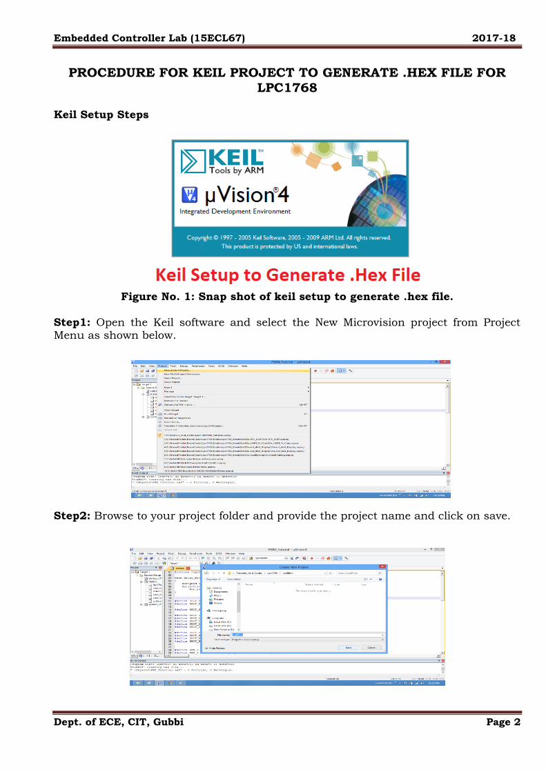
PROCEDURE FOR KEIL PROJECT TO GENERATE .HEX FILE FOR LPC1768
Keil Setup Steps
Figure No. 1: Snap shot of keil setup to generate .hex file.
Step1: Open the Keil software and select the New Microvision project from Project Menu as shown below.
Step2: Browse to your project folder and provide the project name and click on save.
Embedded Controller Lab (15ECL67) 2017-18
Dept. of ECE, CIT, Gubbi Page 3
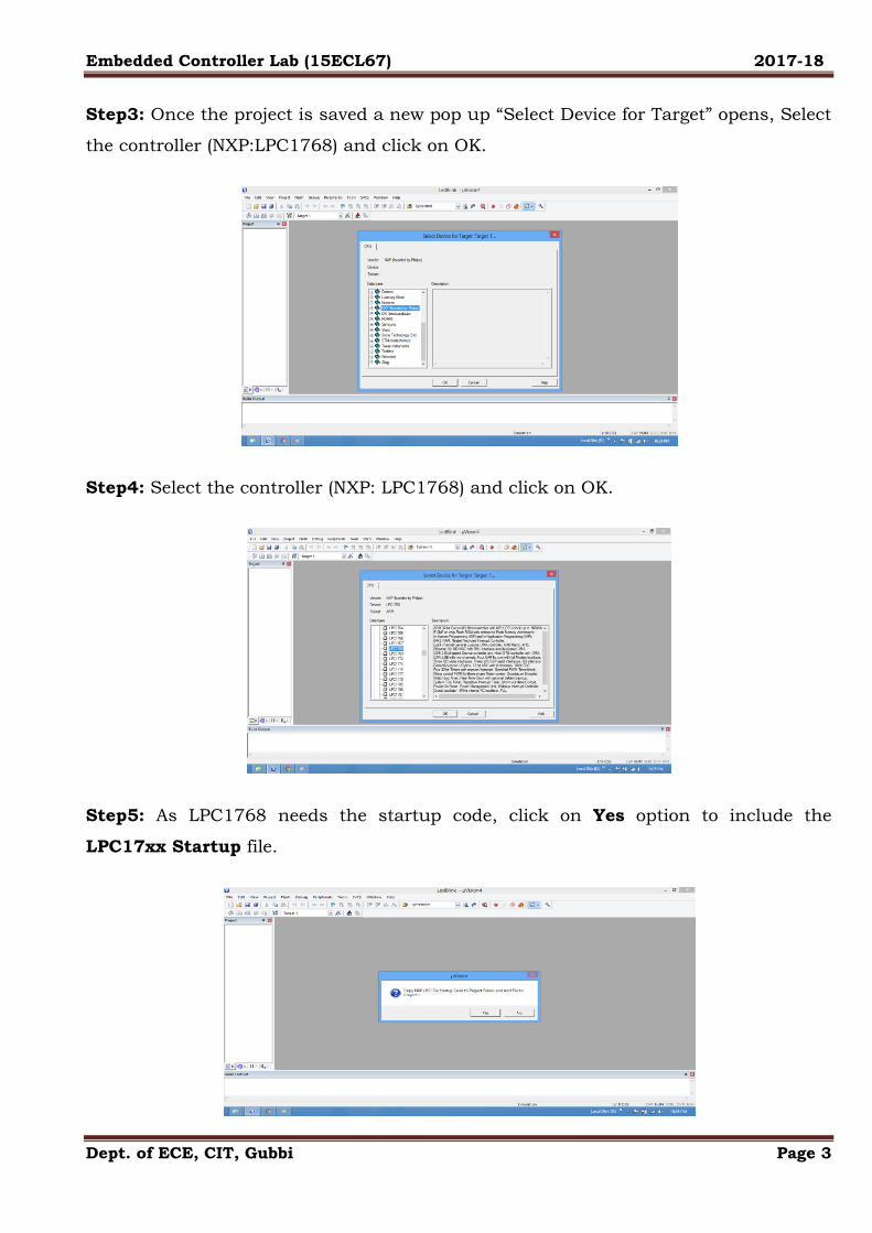
Step3: Once the project is saved a new pop up “Select Device for Target” opens, Select
the controller (NXP:LPC1768) and click on OK.
Step4: Select the controller (NXP: LPC1768) and click on OK.
Step5: As LPC1768 needs the startup code, click on Yes option to include the
LPC17xx Startup file.

Embedded Controller Lab (15ECL67) 2017-18
Dept. of ECE, CIT, Gubbi Page 4
Step6: Create a new file to write the program.
Step7: Type the code or Copy paste the below code snippet.
(Sample led on off main program)
Step8: After typing the code save the file as main.c.

Embedded Controller Lab (15ECL67) 2017-18
Dept. of ECE, CIT, Gubbi Page 5
Step9: Add the recently saved file to the project.
Step10: Add the main.c along with system_LPC17xx.c.
Step11: Build the project and fix the compiler errors/warnings if any.

Embedded Controller Lab (15ECL67) 2017-18
Dept. of ECE, CIT, Gubbi Page 6
Step12: Code is compiled with no errors. The .hex file is still not generated.
Enable Hex File Generation
Step13: Click on Target Options to select the option for generating .hex file.
Step14: Set IROM1 start address as 0x0000.

Embedded Controller Lab (15ECL67) 2017-18
Dept. of ECE, CIT, Gubbi Page 7
Step15: Enable the option to generate the .hex file
Step16: .Hex file is generated after a rebuild.
Step17: Check the project folder for the generated .hex file.
Now .hex file with project name will be generated.

Embedded Controller Lab (15ECL67) 2017-18
Dept. of ECE, CIT, Gubbi Page 8
FLASH MAGIC SOFTWARE INSTALLATION
Install the Flash Magic software provided on the CD. Run the EXE file and
follow the on screen process. Steps to work with Flash Magic Software to execute the application
Open the flash magic software and follow the below steps.
1. Select the IC from Select Menu(LPC1768).
2. Select the COM Port. Check the device manger for detected Com port.
3. Select Baud rate from 9600
4. Select None Isp Option.
5. Oscillator Freq 12.000000(12Mhz).
6. Check the Erase blocks used by Hex file option
7. Browse and Select the hex file.
8. Check the Verify After Programming Option.
9. If DTR and RTS are used then go to Options->Advanced Options-> Hardware
Config and select the Use DTR and RTS Option.
10. Hit the Start Button to flash the hex file.
11. Once the hex file is flashed, Reset the board. Now the controller should
run your application code.
Note: If you want to download a .Hex file then put the Sliding switch SW4 to programming mode and press RESET button once. After downloading the .Hex
files put the switch SW4 to execution mode and press the RESET switch again.

Embedded Controller Lab (15ECL67) 2017-18
Dept. of ECE, CIT, Gubbi Page 9
Experiment No: 1 Date:
ALP TO MULTIPLY TWO 16 BIT BINARY NUMBERS.
TTL Ch5Ex1
Area Program, CODE, READONLY
MAIN
LDR R0, Number1
LDR R1,Number2
Mul R0, R1,R0
MUL R0,R0,R1
STR R0, Result
SWI &11
AREA Data1, DATA
Number1 DCD &706F
Number2 DCD &7016
ALIGN
AREA Data2, DATA
Result DCD
ALIGN
END
Embedded Controller Lab (15ECL67) 2017-18
Dept. of ECE, CIT, Gubbi Page 10
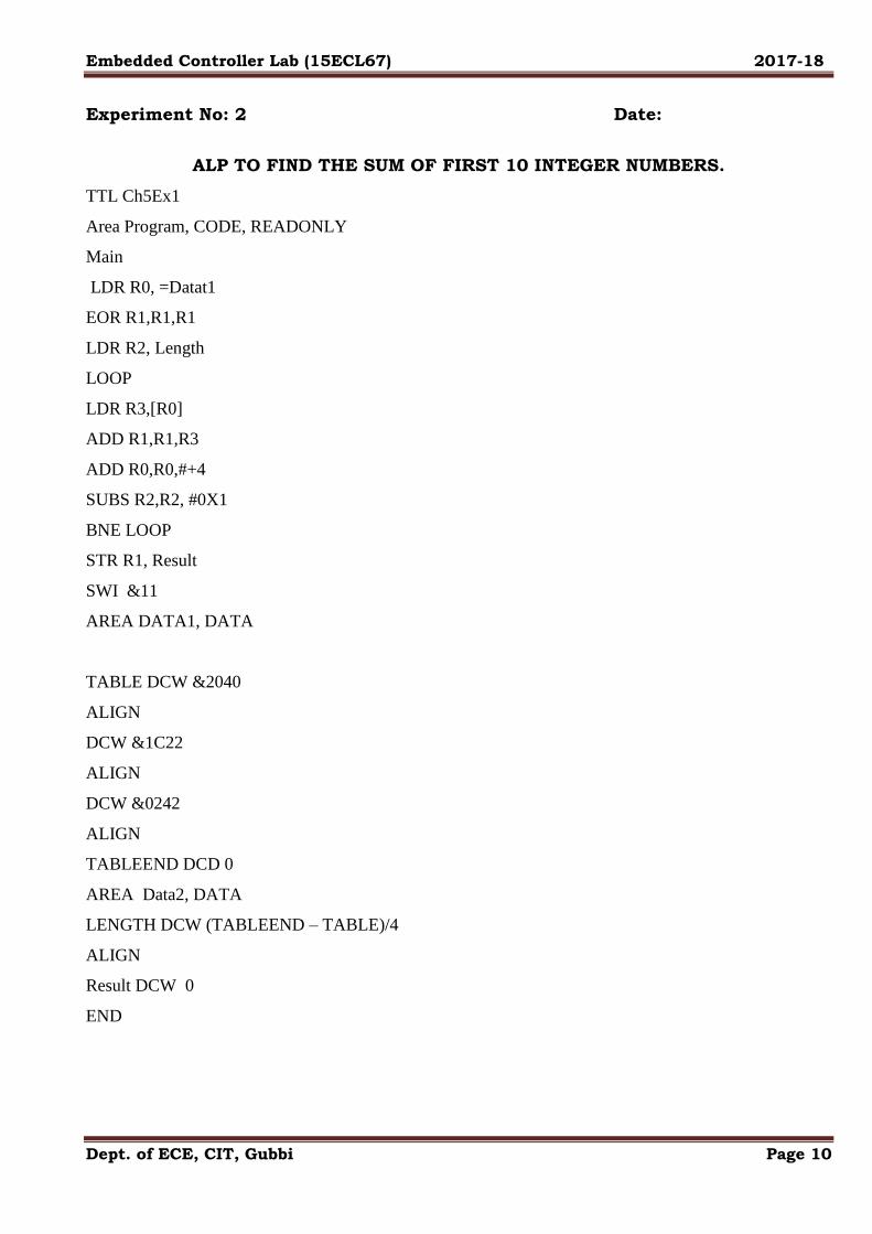
Experiment No: 2 Date:
ALP TO FIND THE SUM OF FIRST 10 INTEGER NUMBERS.
TTL Ch5Ex1
Area Program, CODE, READONLY
Main
LDR R0, =Datat1
EOR R1,R1,R1
LDR R2, Length
LOOP
LDR R3,[R0]
ADD R1,R1,R3
ADD R0,R0,#+4
SUBS R2,R2, #0X1
BNE LOOP
STR R1, Result
SWI &11
AREA DATA1, DATA
TABLE DCW &2040
ALIGN
DCW &1C22
ALIGN
DCW &0242
ALIGN
TABLEEND DCD 0
AREA Data2, DATA
LENGTH DCW (TABLEEND – TABLE)/4
ALIGN
Result DCW 0
END
Embedded Controller Lab (15ECL67) 2017-18
Dept. of ECE, CIT, Gubbi Page 11
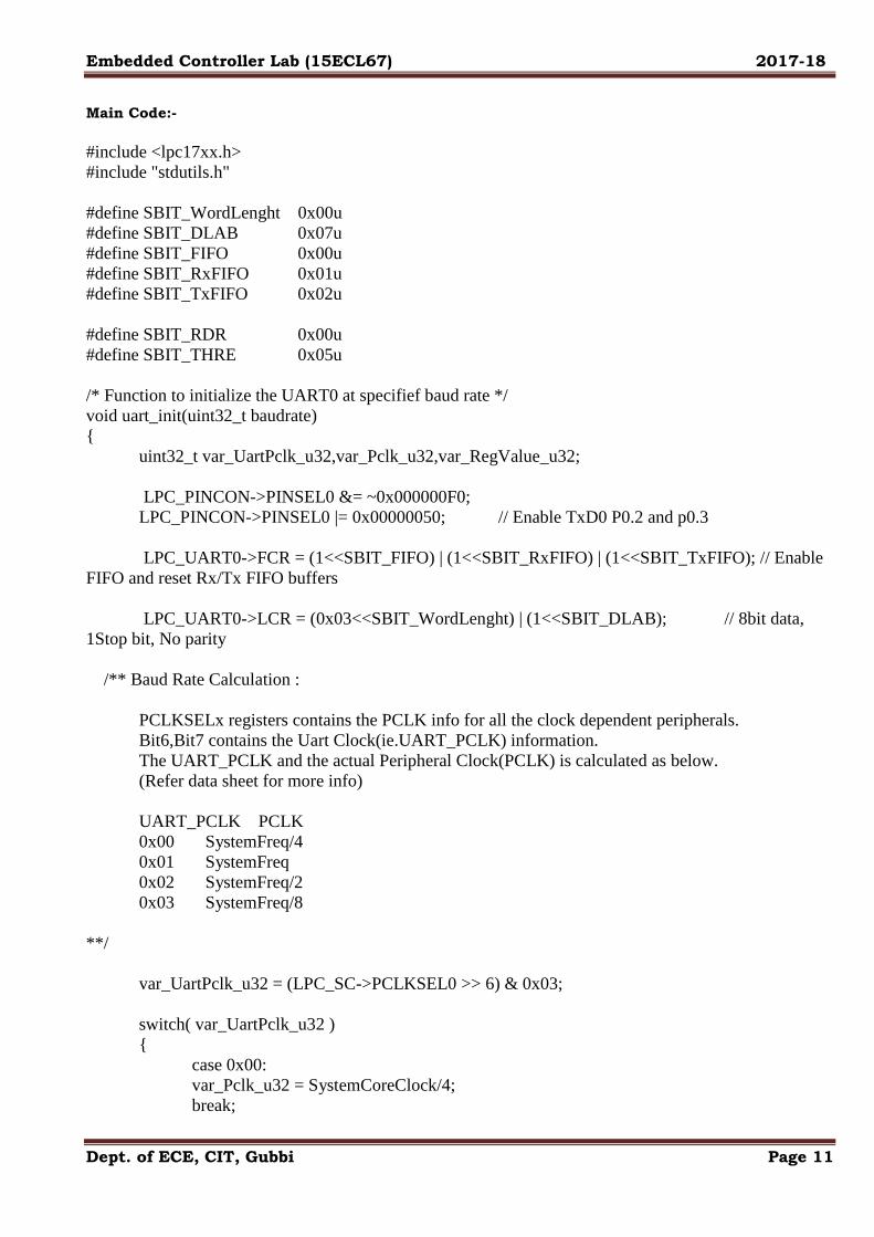
Main Code:-
#include <lpc17xx.h>
#include "stdutils.h"
#define SBIT_WordLenght 0x00u
#define SBIT_DLAB 0x07u
#define SBIT_FIFO 0x00u
#define SBIT_RxFIFO 0x01u
#define SBIT_TxFIFO 0x02u
#define SBIT_RDR 0x00u
#define SBIT_THRE 0x05u
/* Function to initialize the UART0 at specifief baud rate */
void uart_init(uint32_t baudrate)
{
uint32_t var_UartPclk_u32,var_Pclk_u32,var_RegValue_u32;
LPC_PINCON->PINSEL0 &= ~0x000000F0;
LPC_PINCON->PINSEL0 |= 0x00000050; // Enable TxD0 P0.2 and p0.3
LPC_UART0->FCR = (1<<SBIT_FIFO) | (1<<SBIT_RxFIFO) | (1<<SBIT_TxFIFO); // Enable
FIFO and reset Rx/Tx FIFO buffers
LPC_UART0->LCR = (0x03<<SBIT_WordLenght) | (1<<SBIT_DLAB); // 8bit data,
1Stop bit, No parity
/** Baud Rate Calculation :
PCLKSELx registers contains the PCLK info for all the clock dependent peripherals.
Bit6,Bit7 contains the Uart Clock(ie.UART_PCLK) information.
The UART_PCLK and the actual Peripheral Clock(PCLK) is calculated as below.
(Refer data sheet for more info)
UART_PCLK PCLK
0x00 SystemFreq/4
0x01 SystemFreq
0x02 SystemFreq/2
0x03 SystemFreq/8
**/
var_UartPclk_u32 = (LPC_SC->PCLKSEL0 >> 6) & 0x03;
switch( var_UartPclk_u32 )
{
case 0x00:
var_Pclk_u32 = SystemCoreClock/4;
break;

Embedded Controller Lab (15ECL67) 2017-18
Dept. of ECE, CIT, Gubbi Page 12
Experiment No: 1 Date:
DISPLAY “HELLO WORLD” MESSAGE USING INTERNAL UART
LPC1768: UART Programming
Objective
In this tutorial we are going to discuss the serial communication using UART. LPC1768 has four inbuilt
USARTs. We are going to discuss only UART0. After this tutorial you should be able to extend it to
remaining three UARTS.
UART module
UART module and registers. LPC1768 has 4-UARTs numbering 0-3, similarly the pins are also named
as RXD0-RXD3 and TXD0-TXD3.As the LPC1768 pins are multiplexed for multiple functionalities, first
they have to be configured as UART pins.
Below table shows the multiplexed UARTs pins.
Port Pin Pin Number PINSEL_FUNC_0 PINSEL_FUNC_1 PINSEL_FUNC_2 PINSEL_FUNC_3
P0.02 98 GPIO TXD0 ADC0[7]
P0.03 99 GPIO RXD0 ADC0[6]
P2_0 48 GPIO PWM1[1] TXD1
P2.1 49 GPIO PWM1[2] RXD1
P0.10 62 GPIO TXD2 SDA2 MAT3[0]
P0.11 63 GPIO RXD2 SCL2 MAT3[1]
P0.0 82 GPIO CAN1_Rx TXD3 SDA1
P0.1 85 GPIO CAN1_Tx RXD3 SCL1
UART Registers
The below table shows the registers associated with LPC1768 UART.
Register Description
RBR Contains the recently received Data
THR Contains the data to be transmitted
FCR FIFO Control Register
LCR Controls the UART frame formatting(Number of Data Bits, Stop bits)
DLL Least Significant Byte of the UART baud rate generator value.
DLM Most Significant Byte of the UART baud rate generator value.
Embedded Controller Lab (15ECL67) 2017-18
Dept. of ECE, CIT, Gubbi Page 13
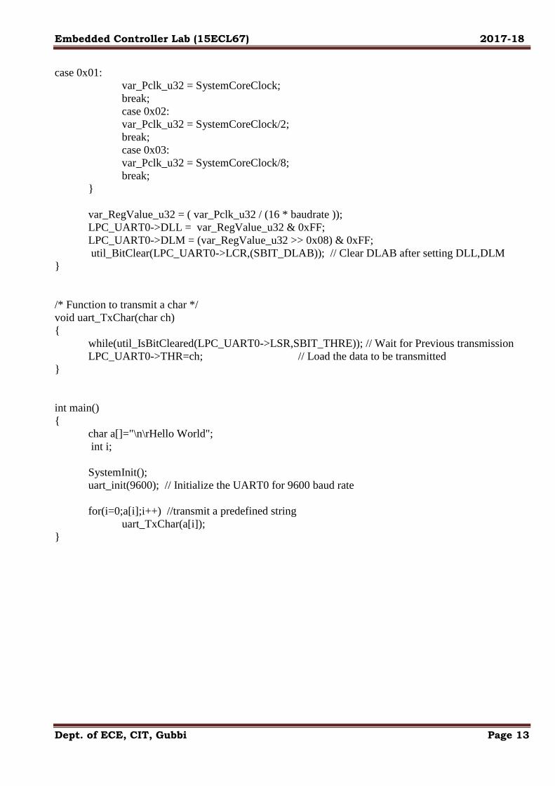
case 0x01:
var_Pclk_u32 = SystemCoreClock;
break;
case 0x02:
var_Pclk_u32 = SystemCoreClock/2;
break;
case 0x03:
var_Pclk_u32 = SystemCoreClock/8;
break;
}
var_RegValue_u32 = ( var_Pclk_u32 / (16 * baudrate ));
LPC_UART0->DLL = var_RegValue_u32 & 0xFF;
LPC_UART0->DLM = (var_RegValue_u32 >> 0x08) & 0xFF;
util_BitClear(LPC_UART0->LCR,(SBIT_DLAB)); // Clear DLAB after setting DLL,DLM
}
/* Function to transmit a char */
void uart_TxChar(char ch)
{
while(util_IsBitCleared(LPC_UART0->LSR,SBIT_THRE)); // Wait for Previous transmission
LPC_UART0->THR=ch; // Load the data to be transmitted
}
int main()
{
char a[]="\n\rHello World";
int i;
SystemInit();
uart_init(9600); // Initialize the UART0 for 9600 baud rate
for(i=0;a[i];i++) //transmit a predefined string
uart_TxChar(a[i]);
}

Embedded Controller Lab (15ECL67) 2017-18
Dept. of ECE, CIT, Gubbi Page 14
UART Register Configuration
Now lets see how to configure the individual registers for UART communication.
FCR ( FIFO Control Register )
LPC1768 has inbuilt 16byte FIFO for Receiver/Transmitter. Thus it can store 16-bytes of data received
on UART without overwriting. If the data is not read before the Queue(FIFO) is filled then the new data
will be lost and the OVERRUN error bit will be set.
FCR
31:8 7:6 5:4 3 2 1 0
RESERVED RX TRIGGER RESERVED DMA MODE TX FIFO RESET RX FIFO RESET FIFO ENABLE
Bit 0 – FIFO:
This bit is used to enable/disable the FIFO for the data received/transmitted.
0--FIFO is Disabled.
1--FIFO is Enabled for both Rx and Tx.
Bit 1 – RX_FIFO:
This is used to clear the 16-byte Rx FIFO.
0--No impact.
1--CLears the 16-byte Rx FIFO and the resets the FIFO pointer.
Bit 2 – Tx_FIFO:
This is used to clear the 16-byte Tx FIFO.
0--No impact.
1--Clears the 16-byte Tx FIFO and the resets the FIFO pointer.
Bit 3 – DMA_MODE:
This is used for Enabling/Disabling DMA mode.
0--Disables the DMA.
1--Enables DMA only when the FIFO(bit-0) bit is SET.
Bit 7:6 – Rx_TRIGGER:
This bit is used to select the number of bytes of the receiver data to be written so as to enable the
interrupt/DMA.
00-- Trigger level 0 (1 character or 0x01)
01-- Trigger level 1 (4 characters or 0x04)
10-- Trigger level 2 (8 characters or 0x08)
11-- Trigger level 3 (14 characters or 0x0E)

Embedded Controller Lab (15ECL67) 2017-18
Dept. of ECE, CIT, Gubbi Page 15
LCR ( Line Control Register )
This register is used for defining the UART frame format ie. Number of Data bits, STOP bits etc.
LCR
31:8 7 6 5:4 3 2 1:0
Reserved DLAB Break COntrol Parity Select Parity Enable Stop Bit Select Word Length Select
Bit 1:0 – WLS : WordLenghtSelect
These two bits are used to select the character length
00-- 5-bit character length
01-- 6-bit character length
10-- 7-bit character length
11-- 8-bit character length
Bit 2 – Stop Bit Selection:
This bit is used to select the number(1/2) of stop bits
0-- 1 Stop bit
1-- 2 Stop Bits
Bit 3 – Parity Enable:
This bit is used to Enable or Disable the Parity generation and checking.
0-- Disable parity generation and checking.
1-- Enable parity generation and checking.
Bit 5:4 – Parity Selection:
These two bits will be used to select the type of parity.
00-- Odd parity. Number of 1s in the transmitted character and the attached parity bit will be odd.
01-- Even Parity. Number of 1s in the transmitted character and the attached parity bit will be even.
10-- Forced "1" stick parity.
11-- Forced "0" stick parity
Bit 6 – Break Control
0-- Disable break transmission.
1-- Enable break transmission. Output pin UARTn TXD is forced to logic 0
Bit 8 – DLAB: Divisor Latch Access Bit
This bit is used to enable the access to divisor latch.
0-- Disable access to divisor latch
0-- Enable access to divisor latch
Embedded Controller Lab (15ECL67) 2017-18
Dept. of ECE, CIT, Gubbi Page 16
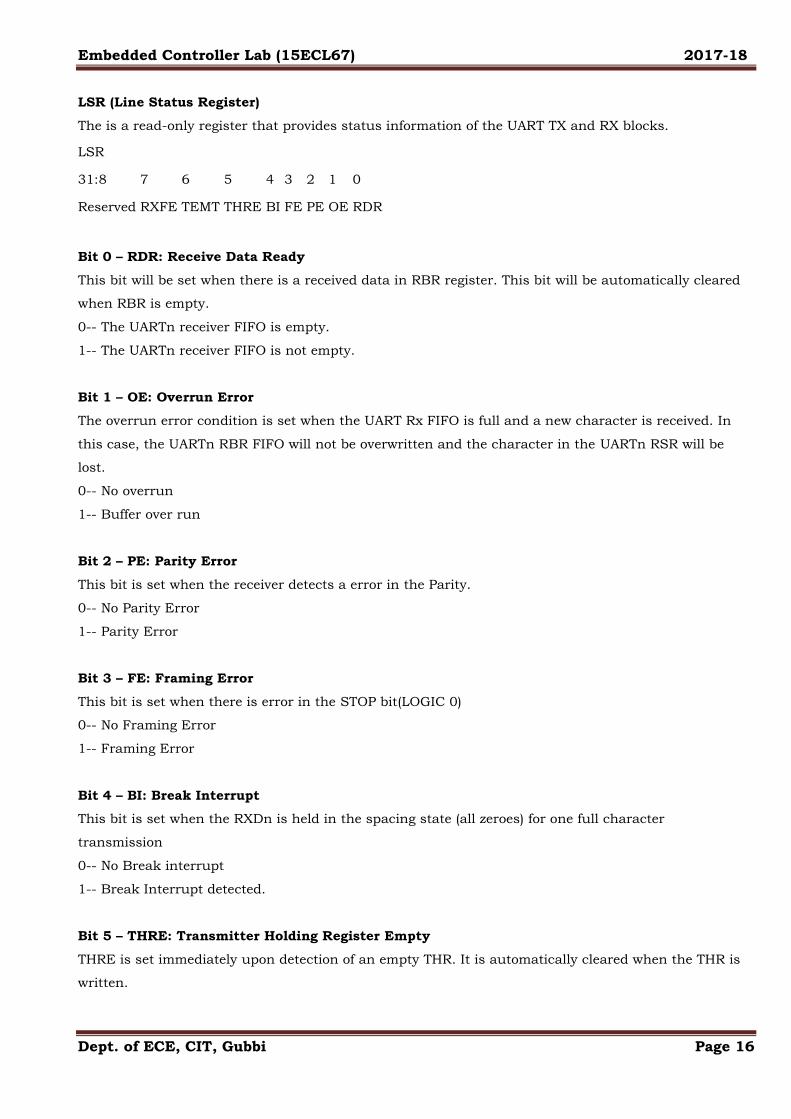
LSR (Line Status Register)
The is a read-only register that provides status information of the UART TX and RX blocks.
LSR
31:8 7 6 5 4 3 2 1 0
Reserved RXFE TEMT THRE BI FE PE OE RDR
Bit 0 – RDR: Receive Data Ready
This bit will be set when there is a received data in RBR register. This bit will be automatically cleared
when RBR is empty.
0-- The UARTn receiver FIFO is empty.
1-- The UARTn receiver FIFO is not empty.
Bit 1 – OE: Overrun Error
The overrun error condition is set when the UART Rx FIFO is full and a new character is received. In
this case, the UARTn RBR FIFO will not be overwritten and the character in the UARTn RSR will be
lost.
0-- No overrun
1-- Buffer over run
Bit 2 – PE: Parity Error
This bit is set when the receiver detects a error in the Parity.
0-- No Parity Error
1-- Parity Error
Bit 3 – FE: Framing Error
This bit is set when there is error in the STOP bit(LOGIC 0)
0-- No Framing Error
1-- Framing Error
Bit 4 – BI: Break Interrupt
This bit is set when the RXDn is held in the spacing state (all zeroes) for one full character
transmission
0-- No Break interrupt
1-- Break Interrupt detected.
Bit 5 – THRE: Transmitter Holding Register Empty
THRE is set immediately upon detection of an empty THR. It is automatically cleared when the THR is
written.

Embedded Controller Lab (15ECL67) 2017-18
Dept. of ECE, CIT, Gubbi Page 17
0-- THR register is Empty
1-- THR has valid data to be transmitted
Bit 6 – TEMT: Transmitter Empty
TEMT is set when both UnTHR and UnTSR are empty; TEMT is cleared when any of them contain valid
data.
0-- THR and/or the TSR contains valid data.
1-- THR and the TSR are empty.
Bit 7 – RXFE: Error in Rx FIFO
This bit is set when the received data is affected by Framing Error/Parity Error/Break Error.
0-- RBR contains no UARTn RX errors.
1-- RBR contains at least one RX error.
TER (Transmitter Enable register)
This register is used to Enable/Disable the transmission
TER
31:8 7 6-0
Reserved TXEN Reserved
Bit 7 – TXEN: Trsnamitter Enable
When this bit is 1, the data written to the THR is output on the TXD pin.
If this bit is cleared to 0 while a character is being sent, the transmission of that character is
completed, but no further characters are sent until this bit is set again.
In other words, a 0 in this bit blocks the transfer of characters.
Note: By default this bit will be set after Reset.
Baudrate Calculation
LPC1768 generates the baud rate depending on the values of DLM,DLL.
Baudrate = PCLK/ (16 * ( 256 * DLM + DLL) * (1+ DivAddVal/MulVal))
Getting the PCLK value.
PCLKSELx registers contains the PCLK info for all the clock dependent peripherals in which Bit6,Bit7
contains the Uart Clock(ie.UART_PCLK) information.
The UART_PCLK and the actual Peripheral Clock(PCLK) is calculated as below.
(Refer data sheet for more info)

Embedded Controller Lab (15ECL67) 2017-18
Dept. of ECE, CIT, Gubbi Page 18
UART_PCLK PCLK
0 SystemFreq/4
1 SystemFreq
2 SystemFreq/2
3 SystemFreq/8
DivAddVal/MulVal == 0
Using the above parameters , DLL/DLM is calculated as below.
(256 * DLL + DLM) = PCLK / (16* Baudrate).
Steps for Configuring UART0
Below are the steps for configuring the UART0.
1. Step1: Configure the GPIO pin for UART0 function using PINSEL register.
2. Step2: Configure the FCR for enabling the FIXO and Reset both the Rx/Tx FIFO.
3. Step3: Configure LCR for 8-data bits, 1 Stop bit, Disable Parity and Enable DLAB.
4. Step4: Get the PCLK from PCLKSELx register 7-6 bits.
5. Step5: Calculate the DLM,DLL values for required baudrate from PCLK.
6. Step6: Update the DLM,DLL with the calculated values.
7. Step6: Finally clear DLAB to disable the access to DLM,DLL.
After this the UART will be ready to Transmit/Receive Data at the specified baudrate.
Result:

Embedded Controller Lab (15ECL67) 2017-18
Dept. of ECE, CIT, Gubbi Page 19
Main code:-
#include <lpc17xx.h>
void delay_ms(unsigned int ms)// delay routine
{
unsigned int i,j;
for(i=0;i<ms;i++)
for(j=0;j<60000;j++);
}
#define SBIT_CNTEN 0 //counter enable
#define SBIT_PWMEN 2 //pwm 2 block enable
#define SBIT_PWMMR0R 1 //This bit is used to Reset PWMTC whenever it Matches PWMRx(x:0-6)
#define SBIT_PWMENA3 11 //This bit is used to enable/disable the PWM output for PWMx(x:1-6)
#define PWM_3 4 //P2_2 (0-1 Bits of PINSEL4)
int main(void)
{
int dutyCycle;
SystemInit();
/* Cofigure pins(P2_2 ) for PWM mode. */
LPC_PINCON->PINSEL4 = (1<<PWM_3) ;
/* Enable Counters,PWM module */
LPC_PWM1->TCR = (1<<SBIT_CNTEN) | (1<<SBIT_PWMEN);
LPC_PWM1->PR = 0x00; /* No Prescalar */
LPC_PWM1->MCR = (1<<SBIT_PWMMR0R); /*Reset on PWMMR0, reset TC if it matches MR0 */
LPC_PWM1->MR0 = 100; /* set PWM cycle(Ton+Toff)=100) */
/* Enable the PWM output pins for PWM_1-PWM_4(P2_0 - P2_3) */
LPC_PWM1->PCR = (1<<SBIT_PWMENA3);
while(1)
{
{
LPC_PWM1->MR3 = dutyCycle; /* Increase the dutyCycle from 0-100 */
delay_ms(5);
}
if(!(LPC_GPIO2->FIOPIN & 0x00000800))//if sw 23 pressed
{
while(!(LPC_GPIO2->FIOPIN & 0x00000800));
dutyCycle-=10; //decrement duty cycle 10%
if(dutyCycle<0)
{
dutyCycle=0;
}
}
else if(!(LPC_GPIO2->FIOPIN & 0x00001000)) //if SW 22 pressed
Embedded Controller Lab (15ECL67) 2017-18
Dept. of ECE, CIT, Gubbi Page 20
Experiment No: 2 Date:
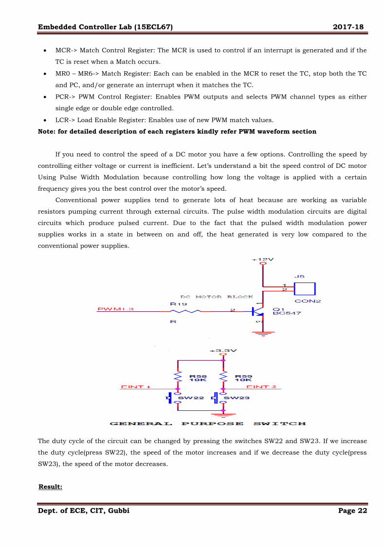
INTERFACE AND CONTROL A DC MOTOR
DC Motor Control using PWM of LPC1768
In most of the applications controlling the speed of DC motor is essential where the precision
and protection are the essence. Here we will use the PWM technique to control the speed of the motor
LPC1768 has one PWM channel with six ports. PWM changes the average output voltage by fast
switching. By changing the on time, the output voltage can be 0 to 100%. There are two software
parameters that need a little explanation: cycle and offset. Cycle is the length of a PWM duty cycle and
offset is the on time of a duty cycle.
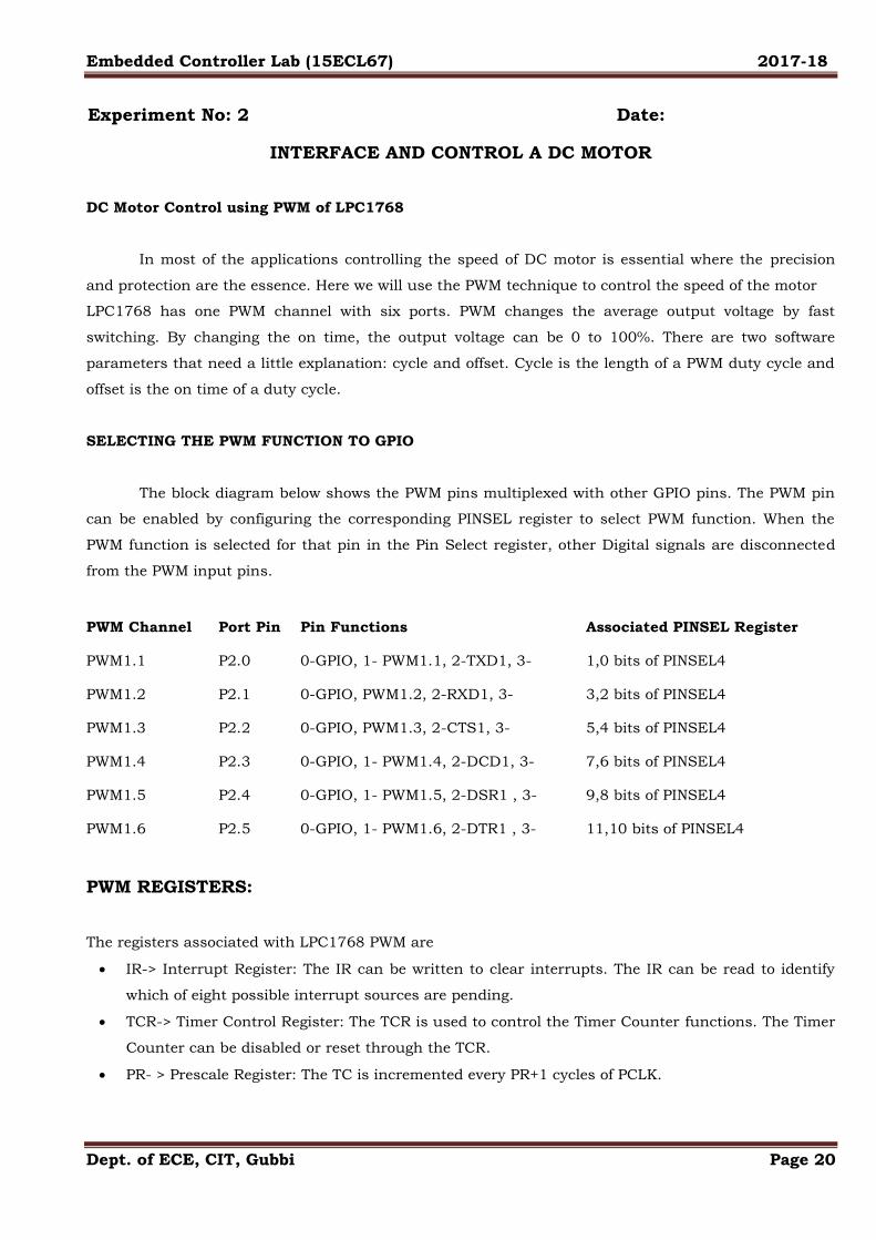
SELECTING THE PWM FUNCTION TO GPIO
The block diagram below shows the PWM pins multiplexed with other GPIO pins. The PWM pin
can be enabled by configuring the corresponding PINSEL register to select PWM function. When the
PWM function is selected for that pin in the Pin Select register, other Digital signals are disconnected
from the PWM input pins.
PWM Channel Port Pin Pin Functions Associated PINSEL Register
PWM1.1 P2.0 0-GPIO, 1- PWM1.1, 2-TXD1, 3- 1,0 bits of PINSEL4
PWM1.2 P2.1 0-GPIO, PWM1.2, 2-RXD1, 3- 3,2 bits of PINSEL4
PWM1.3 P2.2 0-GPIO, PWM1.3, 2-CTS1, 3- 5,4 bits of PINSEL4
PWM1.4 P2.3 0-GPIO, 1- PWM1.4, 2-DCD1, 3- 7,6 bits of PINSEL4
PWM1.5 P2.4 0-GPIO, 1- PWM1.5, 2-DSR1 , 3- 9,8 bits of PINSEL4
PWM1.6 P2.5 0-GPIO, 1- PWM1.6, 2-DTR1 , 3- 11,10 bits of PINSEL4
PWM REGISTERS:
The registers associated with LPC1768 PWM are
IR-> Interrupt Register: The IR can be written to clear interrupts. The IR can be read to identify
which of eight possible interrupt sources are pending.
TCR-> Timer Control Register: The TCR is used to control the Timer Counter functions. The Timer
Counter can be disabled or reset through the TCR.
PR- > Prescale Register: The TC is incremented every PR+1 cycles of PCLK.

Embedded Controller Lab (15ECL67) 2017-18
Dept. of ECE, CIT, Gubbi Page 21
{
while(!(LPC_GPIO2->FIOPIN & 0x00001000));
dutyCycle+=10; //increment duty cycle 10%
if(dutyCycle>100)
{
dutyCycle=99;
}
}
}
}
Embedded Controller Lab (15ECL67) 2017-18
Dept. of ECE, CIT, Gubbi Page 22
MCR-> Match Control Register: The MCR is used to control if an interrupt is generated and if the
TC is reset when a Match occurs.
MR0 – MR6-> Match Register: Each can be enabled in the MCR to reset the TC, stop both the TC
and PC, and/or generate an interrupt when it matches the TC.
PCR-> PWM Control Register: Enables PWM outputs and selects PWM channel types as either
single edge or double edge controlled.
LCR-> Load Enable Register: Enables use of new PWM match values.
Note: for detailed description of each registers kindly refer PWM waveform section
If you need to control the speed of a DC motor you have a few options. Controlling the speed by
controlling either voltage or current is inefficient. Let‟s understand a bit the speed control of DC motor
Using Pulse Width Modulation because controlling how long the voltage is applied with a certain
frequency gives you the best control over the motor‟s speed.
Conventional power supplies tend to generate lots of heat because are working as variable
resistors pumping current through external circuits. The pulse width modulation circuits are digital
circuits which produce pulsed current. Due to the fact that the pulsed width modulation power
supplies works in a state in between on and off, the heat generated is very low compared to the
conventional power supplies.
The duty cycle of the circuit can be changed by pressing the switches SW22 and SW23. If we increase
the duty cycle(press SW22), the speed of the motor increases and if we decrease the duty cycle(press
SW23), the speed of the motor decreases.
Result:
Embedded Controller Lab (15ECL67) 2017-18
Dept. of ECE, CIT, Gubbi Page 23
Main code: - Step Angle Rotation
#include <lpc17xx.h>
void delay(unsigned int ms)
{
unsigned int i,j;
for(i=0;i<ms;i++)
for(j=0;j<20000;j++); //delay subroutine
}
/* start the main program */
int main()
{
int cycle;
SystemInit(); //Clock and PLL configuration
LPC_GPIO0->FIODIR |= 0x00078000; //Configure the PORT0 pins as OUTPUT;
for(cycle=0; cycle<13; cycle++) // for loop condition for number of rotation. It gives approx 90 degree rotation
{
LPC_GPIO0->FIOPIN = 0x00008000 ; // p0.15 pin
delay(100);
LPC_GPIO0->FIOPIN = 0x00010000 ; // p0.16 pin
delay(100);
LPC_GPIO0->FIOPIN = 0x00020000 ; //p0.17 pin
delay(100);
LPC_GPIO0->FIOPIN = 0x00040000 ; // p0.18 pin
delay(100);
}
}
Stepper motor rotation clockwise and anticlockwise.
#include "lpc17xx.h"
void delay();
void delay()
{
int i,j;
for(i=0;i<0xff;i++)
for(j=0;j<0x400;j++);
}
int main (void)
{
char rotate=0;
SystemInit();
LPC_GPIO0->FIODIR |= 0x00078000;
while(1)
{
if(rotate==1)
{
LPC_GPIO0->FIOPIN = 0x00008000 ;

Embedded Controller Lab (15ECL67) 2017-18
Dept. of ECE, CIT, Gubbi Page 24
Experiment No: 3 Date:
INTERFACE A STEPPER MOTOR AND ROTATE IT IN CLOCKWISE AND ANTI-
CLOCKWISE DIRECTION Stepper motor
A stepper motor or step motor or stepping motor is a brushless DC electric motor that divides a
full rotation into a number of equal steps. The motor's position can then be commanded to move and
hold at one of these steps without any position sensor for feedback (an open-loop controller), as long as
the motor is carefully sized to the application in respect to torque and speed.
What is a stepper motor?
A Stepper Motor or a step motor is a brushless, synchronous motor which divides a full rotation
into a number of steps. Unlike a brushless DC motor which rotates continuously when a fixed DC
voltage is applied to it, a step motor rotates in discrete step angles. The Stepper Motors therefore are
manufactured with steps per revolution of 12, 24, 72, 144, 180, and 200, resulting in stepping angles
of 30, 15, 5, 2.5, 2, and 1.8 degrees per step. The stepper motor can be controlled with or without
feedback.
How a stepper motor works?
Stepper motors work on the principle of electromagnetism. There is a soft iron or magnetic rotor
shaft surrounded by the electromagnetic stators. The rotor and stator have poles which may be teethed
or not depending upon the type of stepper. When the stators are energized the rotor moves to align
itself along with the stator (in case of a permanent magnet type stepper) or moves to have a minimum
gap with the stator (in case of a variable reluctance stepper). This way the stators are energized in a
sequence to rotate the stepper motor. Get more information about working of stepper motors through
interesting images at the stepper motor Insight.
delay();
LPC_GPIO0->FIOPIN = 0x00010000 ;

Embedded Controller Lab (15ECL67) 2017-18
Dept. of ECE, CIT, Gubbi Page 25
delay();
LPC_GPIO0->FIOPIN = 0x00020000 ;
delay();
LPC_GPIO0->FIOPIN = 0x00040000 ;
delay();
}
else
{
LPC_GPIO0->FIOPIN = 0x00040000 ;
delay();
LPC_GPIO0->FIOPIN = 0x00020000 ;
delay();
LPC_GPIO0->FIOPIN = 0x00010000 ;
delay();
LPC_GPIO0->FIOPIN = 0x00008000 ;
delay();
}
if(!(LPC_GPIO2->FIOPIN & 0x00000800))
{
while(!(LPC_GPIO2->FIOPIN & 0x00000800));
rotate=1;
}
else if(!(LPC_GPIO2->FIOPIN & 0x00001000))
{
while(!(LPC_GPIO2->FIOPIN & 0x00001000));
rotate=0;
}
}
}

Embedded Controller Lab (15ECL67) 2017-18
Dept. of ECE, CIT, Gubbi Page 26
What are stepper motors good for?
Positioning – Since steppers move in precise repeatable steps, they excel in applications
requiring precise positioning such as 3D printers, CNC, Camera platforms and X,Y Plotters.
Some disk drives also use stepper motors to position the read/write head.
Speed Control – Precise increments of movement also allow for excellent control of rotational
speed for process automation and robotics.
Low Speed Torque - Normal DC motors don't have very much torque at low speeds. A Stepper
motor has maximum torque at low speeds, so they are a good choice for applications requiring
low speed with high precision.
How Stepper Motors Work?
Stepper motors consist of a permanent magnetic rotating shaft, called the rotor, and
electromagnets on the stationary portion that surrounds the motor, called the stator. Figure 1
illustrates one complete rotation of a stepper motor. At position 1, we can see that the rotor is
beginning at the upper electromagnet, which is currently active (has voltage applied to it). To move the
rotor clockwise (CW), the upper electromagnet is deactivated and the right electromagnet is activated,
causing the rotor to move 90 degrees CW, aligning itself with the active magnet. This process is
repeated in the same manner at the south and west electromagnets until we once again reach the
starting position.
Figure 1
In the above example, we used a motor with a resolution of 90 degrees or demonstration
purposes. In reality, this would not be a very practical motor for most applications. The average
stepper motor's resolution -- the amount of degrees rotated per pulse -- is much higher than

Embedded Controller Lab (15ECL67) 2017-18
Dept. of ECE, CIT, Gubbi Page 27
this. For example, a motor with a resolution of 1.8 degrees would move its rotor 1.8 degrees per
step, thereby requiring 200 pulses (steps) to complete a full 360 degree rotation.
Here we are using 200 pole stepper motor hence it gives 360degree/200 pole=1.8 degree per step.
So for example if we need 120 degree rotation then we have to apply approximately 67 pulses to
complete 120 degree rotation
120/1.8=66.66==67 steps approximately.
Here one cycle means 4 steps. So if we need 90 degree rotation then 90/1.8=50 steps.
Here one cycle means 4 steps. So 50/4=12.5 =~ 13. So we need 13 cycles to rotate 90 degree.
If we want to run 180 degree then 180/1.8=100. So 100/4=25 cycles would make a stepper motor to
rotate 180 degree.

Embedded Controller Lab (15ECL67) 2017-18
Dept. of ECE, CIT, Gubbi Page 28
Result:

Embedded Controller Lab (15ECL67) 2017-18
Dept. of ECE, CIT, Gubbi Page 29
Triangle wave generation:-
#include "LPC17xx.h"
uint32_t val;
int main()
{
SystemInit();
LPC_PINCON->PINSEL1 |= 0x02<<20; //p0.26 pinsel bits 20 and 21
while(1)
{
while(1)
{
val++; // increment values by 6
LPC_DAC->DACR=(val<<6); //send values to dac
if(val>=0x3ff) // if value exceeds 1024
{
break;
}
}
while(1)
{
val--; // decrement value by 6
LPC_DAC->DACR=(val<<6); // send value to dac
if(val<=0x000) // if value come down by 0
{
break;
}
}
}
}
Square Wave generation:-
#include "LPC17xx.h"
void delay(unsigned int ms)// delay subroutine
{
unsigned int i,j;
for(i=0;i<ms;i++)
for(j=0;j<2000;j++);
}
int main()
{
SystemInit();
LPC_PINCON->PINSEL1 |= 0x02<<20; //p0.26 pinsel bits 20 and 21
while(1)
{
LPC_DAC->DACR=0xffff; // send maximum values to dac
delay(20); // delay
LPC_DAC->DACR=0x0000; // send min values to dac
delay(20);
}
}

Embedded Controller Lab (15ECL67) 2017-18
Dept. of ECE, CIT, Gubbi Page 30
Experiment No: 4 Date:
INTERFACE A DAC AND GENERATE TRIANGULAR AND SQUARE WAVEFORMS
LPC1768 DAC Programming Tutorial
In this article, we will go through a discussion on ARM Cortex-M3 LPC1768 DAC programming
tutorial. As you might be knowing, DAC stands for Digital to Analog Conversion. The DAC block in ARM
Cortex-M3 LPC176x microcontroller is one of the simplest to program and also supports DMA(direct
memory access). This tutorial is also applicable for LPC1769 MCU. Basically we assign a digital value to
a register and the DAC block outputs it equivalent analog signal as shown below:
LPC1768/LPC1769 DAC Block
ARM Cortex-M3 LPC176x MCUs incorporate a 10 bit DAC and provide buffered analog output.
As per the datasheet, it is implemented as a string DAC which is the most simplest form of DAC
consisting of 2N resistors in series where N = no. of bits which simply forms a Kelvin-Varley Divider.
LPC176x DAC has only 1 output pin, referred to as AOUT. The Analog voltage at the output of this pin
is given as:
Where VALUE is the 10-bit digital value which is to be converted into its Analog counterpart
and VREF is the input reference voltage.
Embedded Controller Lab (15ECL67) 2017-18
Dept. of ECE, CIT, Gubbi Page 31
Pins relating to LPC1768 DAC block:
Pin Description
AOUT
(P0.26)
Analog Output pin. Provides the converted Analog signal which is referenced to VSSA i.e. the
Analog GND. Set Bits[21:20] in PINSEL1 register to [10] to enable this function.
VREFP,
VREFN
These are reference voltage input pins used for both ADC and DAC. VREFP is positive
reference voltage and VREFN is negative reference voltage pin. In example shown below we will
use VREFN=0V(GND).
VDDA, VSSA VDDA is Analog Power pin and VSSA is Ground pin used to power the ADC module. These are
generally same as VCC and GND but with additional filtering to reduce noise.
DAC Registers in ARM Cortex-M3 LPC176x
The DAC module in ARM LPC1768/LPC1769 has 3 registers viz. DACR, DACCTRL,
DACCNTVAL. In this tutorial we will only go through to DACR register since the other two are related
with DMA operation, explaining which is not in the scope of this tutorial. Just note that DMA is used to
update new values to DACR from memory without the intervention of CPU. This is particularly useful
when generation different types of waveforms using DAC. We will cover this in another tutorial.
Also note that the DAC doesn‟t have a power control it in PCONP register. Simply select the AOUT
alternate function for pin P0.26 using PINSEL1 register to enable DAC output.
The DACR register in LPC1768
The field containing bits [15:6] is used to feed a digital value which needs to be converted and bit 16
is used to select settling time. The bit significance is as shown below:
1. Bit[5:0]: Reserved.
2. Bit[15:6] – VALUE: After a new VALUE is written to this field, given settling time selected using
BIAS has elapsed, we get the converted Analog voltage at the output. The formula for analog
voltage at AOUT pin is as shown above.
3. Bit[16] – BIAS: Setting this bit to 0 selects settling time of 1us max with max current
consumption of 700uA at max 1Mhz update rate. Setting it to 1 will select settling time of 2.5us
but with reduce max current consumption of 300uA at max 400Khz update rate.
4. Bits[31:17]: Reserved
ARM Cortex-M3 LPC1768 DAC example
As evident, without using DMA, programming the DAC block is very straight forward. We just
need to select AOUT function for P0.26 pin and apply a 10-bit value which needs to be converted into
its Analog form. Lets see a basic LPC1768 DAC example. For most development boards VREFP will be
Embedded Controller Lab (15ECL67) 2017-18
Dept. of ECE, CIT, Gubbi Page 32
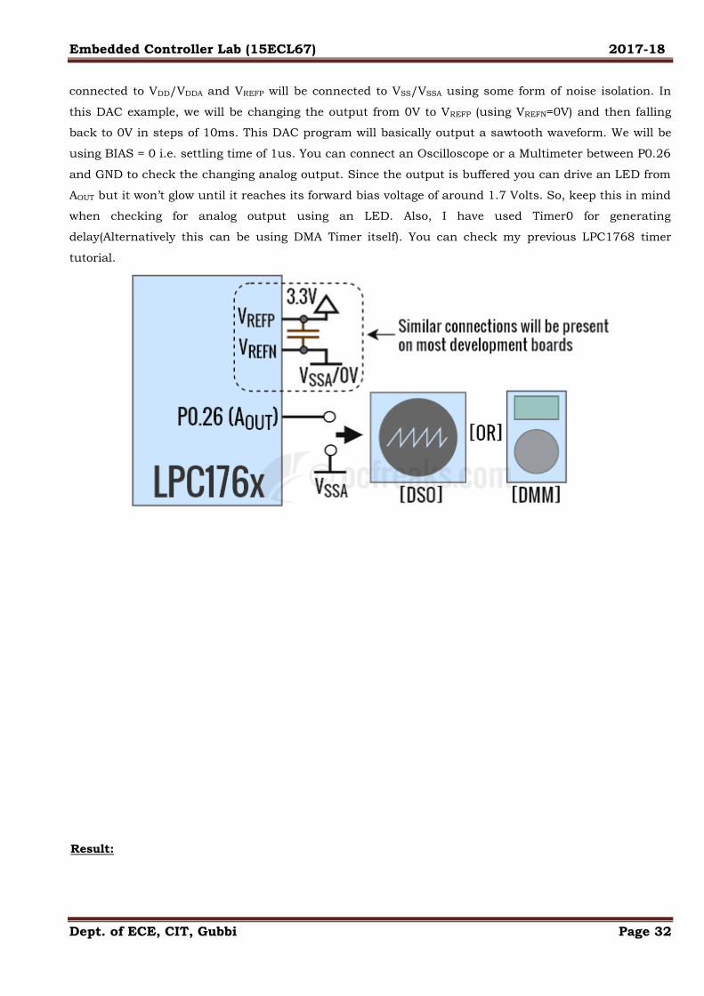
connected to VDD/VDDA and VREFP will be connected to VSS/VSSA using some form of noise isolation. In
this DAC example, we will be changing the output from 0V to VREFP (using VREFN=0V) and then falling
back to 0V in steps of 10ms. This DAC program will basically output a sawtooth waveform. We will be
using BIAS = 0 i.e. settling time of 1us. You can connect an Oscilloscope or a Multimeter between P0.26
and GND to check the changing analog output. Since the output is buffered you can drive an LED from
AOUT but it won‟t glow until it reaches its forward bias voltage of around 1.7 Volts. So, keep this in mind
when checking for analog output using an LED. Also, I have used Timer0 for generating
delay(Alternatively this can be using DMA Timer itself). You can check my previous LPC1768 timer
tutorial.
Result:
Embedded Controller Lab (15ECL67) 2017-18
Dept. of ECE, CIT, Gubbi Page 33
Main code:-
#include "lpc17xx.h"
#include "lcd.h"
/////////////////////////////////////////////
// Matrix Keypad Scanning Routine
//
// COL1 COL2 COL3 COL4
// 0 1 2 3 ROW 1
// 4 5 6 7 ROW 2
// 8 9 A B ROW 3
// C D E F ROW 4
//////////////////////////////////////////////
#define COL1 0
#define COL2 1
#define COL3 4
#define COL4 8
#define ROW1 9
#define ROW2 10
#define ROW3 14
#define ROW4 15
#define COLMASK ((1<<COL1) |(1<< COL2) |(1<< COL3) |(1<< COL4))
#define ROWMASK ((1<<ROW1) |(1<< ROW2) |(1<< ROW3) |(1<< ROW4))
#define KEY_CTRL_DIR LPC_GPIO1->FIODIR
#define KEY_CTRL_SET LPC_GPIO1->FIOSET
#define KEY_CTRL_CLR LPC_GPIO1->FIOCLR
#define KEY_CTRL_PIN LPC_GPIO1->FIOPIN
/////////////// COLUMN WRITE /////////////////////
void col_write( unsigned char data )
{
unsigned int temp=0;
temp=(data) & COLMASK;
KEY_CTRL_CLR |= COLMASK;
KEY_CTRL_SET |= temp;
}
///////////////////////////////// MAIN ///////////////////////////////////////
int main (void)
{
unsigned char key, i;
unsigned char rval[] = {0x77,0x07,0x0d};
unsigned char keyPadMatrix[] =
{
'4','8','B','F',
'3','7','A','E',
'2','6','0','D',
'1','5','9','C'
};

Embedded Controller Lab (15ECL67) 2017-18
Dept. of ECE, CIT, Gubbi Page 34
Experiment No: 5 Date:
INTERFACE A 4X4 KEYBOARD AND DISPLAY THE KEY CODE ON AN LCD
Introduction 4x4 matrix keypad interface:-
There are various methods to provide an input for the GPIO pins of a microcontroller which can
be software controlled or hardware controlled. We have seen a hardware controlled method by taking
an input from a switch or a press button. Push Button Interfacing with LPC1768
The keypad is another external input device which is hardware controlled, but is used for a specific
purpose. In this tutorial we take a look at how a 4×4 matrix keypad is interfaced with the LPC1768
microcontroller. The input taken from the matrix keypad will be displayed on a 16x2 LCD display.
Basic Configuration
NOTE: Please read this section carefully as it is important to understand the hardware connection
before writing software for this application.
As we are using a 4×4 matrix keypad, a total of 8 input-output pins of the micro-controller will
be required for interfacing.
One half of the 8 pins will be hardware controlled and the other half will be software controlled.
Therefore, the columns can be pulled up or pulled down. The rows are the four LSBs of the 8 bit
pins and the columns are the MSBs of the 8 bit pins.
(GENERAL CONVENTION: ROWS: Horizontal & COLUMNS: Vertical)
In our program, the MSBs (columns) will be set in the input mode and the LSBs (rows) will be
set in the output mode. The default state of the MSBs can be HIGH or LOW based on the
hardware connection. Based on this we have two modes of operation for the keypad, i.e. Pull Up
mode or Pull Down mode (refer the fig.). In the pull up mode, MSBs (columns) by default will be
high and in the pull down mode, MSBs by default will be low. We will be operating in the Pull
Up Mode.
Embedded Controller Lab (15ECL67) 2017-18
Dept. of ECE, CIT, Gubbi Page 35
SystemInit();
init_lcd();
KEY_CTRL_DIR |= COLMASK; //Set COLs as Outputs
KEY_CTRL_DIR &= ~(ROWMASK); // Set ROW lines as Inputs
lcd_putstring16(0,"Press HEX Keys..");// 1st line display
lcd_putstring16(1,"Key Pressed = ");// 2nd
line display
while (1)
{
key = 0;
for( i = 0; i < 4; i++ )
{
// turn on COL output one by one
col_write(rval[i]);
// read rows - break when key press detected
if (!(KEY_CTRL_PIN & (1<<ROW1)))
break;
key++;
if (!(KEY_CTRL_PIN & (1<<ROW2)))
break;
key++;
if (!(KEY_CTRL_PIN & (1<<ROW3)))
break;
key++;
if (!(KEY_CTRL_PIN & (1<<ROW4)))
break;
key++;
}
if (key == 0x10)
lcd_putstring16(1,"Key Pressed = ");
else
{
lcd_gotoxy(1,14);
lcd_putchar(keyPadMatrix[key]);
}
}
}

Embedded Controller Lab (15ECL67) 2017-18
Dept. of ECE, CIT, Gubbi Page 36
When a key is pressed, the output and input line or in other words, rows and columns common
to the pressed key will be connected to each other and hence the value on the output line will be
reflected on the corresponding input line.
Without any software change, the columns, which we will be configuring as input pins in the
software, will continue to be in the pulled up state. Therefore, when any key is pressed our aim
is to cause a deviation from this default state. This change is performed in the software.
When a software change occurs and a value is written on the output pins (rows), the four rows
will reflect the value from the controller. This value gets passed to the corresponding column
when the key common to the row and column is pressed. As we are operating in pull up state,
we will continuously send a LOW state to each of the four output pins (rows) keeping all other
pins HIGH.
For every LOW state to each rows, we scan for a key press by checking for a LOW state at any of
the column pins. This is because, when the rows and columns get connected, the circuit takes
the path of least resistance (internal pull up when configured in the input mode is weak) and
the LOW state on the row is reflected on the corresponding column, thus deviating from the
default state. Based on this change in the state of the signal on the respective input line
(column), we can determine the identity of the pressed key.
Firmware
These are the definitions that will be used for the keypad programming.
Keypad Definitions
Next, we must set the direction of the hardware pins according to its software functionality. As
discussed, the LSB (rows) is set in the output mode and the MSB (columns) will be set in the
input mode. The KEYPAD_DATA_MASK definition is used to set the pin direction.
We will be using the UART0 built in module to display the output of the keypad press. Therefore
we must initialize the UART0 communication protocol as well.
The GetKey() performs a continuous scan and checks for a key press. The design logic is based
on the following figure of the keypad connection and the functioning is as follows.
o The ROWS are the LSB pins and the COLUMNS are the MSB pins.

Embedded Controller Lab (15ECL67) 2017-18
Dept. of ECE, CIT, Gubbi Page 37
LCD code:-
#include "lpc17xx.h"
#include "lcd.h"
void Lcd_CmdWrite(unsigned char cmd);
void Lcd_DataWrite(unsigned char dat);
#define LCDRS 9
#define LCDRW 10
#define LCDEN 11
#define LCD_D4 19
#define LCD_D5 20
#define LCD_D6 21
#define LCD_D7 22
#define LcdData LPC_GPIO0->FIOPIN
#define LcdControl LPC_GPIO0->FIOPIN
#define LcdDataDirn LPC_GPIO0->FIODIR
#define LcdCtrlDirn LPC_GPIO0->FIODIR
#define LCD_ctrlMask ((1<<LCDRS)|(1<<LCDRW)|(1<<LCDEN))
#define LCD_dataMask ((1<<LCD_D4)|(1<<LCD_D5)|(1<<LCD_D6)|(1<<LCD_D7))
void delay(unsigned int count)
{
int j=0, i=0;
for (j=0;j<count;j++)
for (i=0;i<30;i++);
}
void sendNibble(char nibble)
{
LcdData&=~(LCD_dataMask); // Clear previous data
LcdData|= (((nibble >>0x00) & 0x01) << LCD_D4);
LcdData|= (((nibble >>0x01) & 0x01) << LCD_D5);
LcdData|= (((nibble >>0x02) & 0x01) << LCD_D6);
LcdData|= (((nibble >>0x03) & 0x01) << LCD_D7);
}
void Lcd_CmdWrite(unsigned char cmd)
{
sendNibble((cmd >> 0x04) & 0x0F); //Send higher nibble
LcdControl &= ~(1<<LCDRS); // Send LOW pulse on RS pin for selecting Command register
LcdControl &= ~(1<<LCDRW); // Send LOW pulse on RW pin for Write operation
LcdControl |= (1<<LCDEN); // Generate a High-to-low pulse on EN pin
delay(100);
LcdControl &= ~(1<<LCDEN);
delay(10000);
sendNibble(cmd & 0x0F); //Send Lower nibble
LcdControl &= ~(1<<LCDRS); // Send LOW pulse on RS pin for selecting Command register
LcdControl &= ~(1<<LCDRW); // Send LOW pulse on RW pin for Write operation
LcdControl |= (1<<LCDEN); // Generate a High-to-low pulse on EN pin
delay(100);
LcdControl &= ~(1<<LCDEN);
delay(1000);
}

Embedded Controller Lab (15ECL67) 2017-18
Dept. of ECE, CIT, Gubbi Page 38
o Since, the MSB is hardware controlled (pull up or pull down), these bits on the keypad
will only take the logic value set in the hardware (LOGIC HIGH in our case).
o When a key is pressed, the corresponding row and column will be connected.
o We will be writing and shifting LOGIC 0 continuously to row „n‟ keeping all the other row
pins at LOGIC 1. (n: 1-4)
o When a key is pressed and LOGIC 0 appears on the corresponding row pin, LOGIC 0
from the row will be reflected to the corresponding column.
o Since the columns are set as input pins in the microcontroller, while reading the values
of the rows, if any of the pin is at LOGIC 0, then it is an indication that a key has been
pressed. The reading operation is done by readbite() function.
o The readbite() uses a switch to identify the row corresponding to the pressed key. If any
of the switch case is satisfied, then it checks for the column corresponding to the
pressed key. If the column reflects a LOGIC 0, then we can determine the value of the
pressed key.
o Now, using a while loop, we will wait till the LOGIC 0 disappears so that the software
waits till the current state in the hardware is changed. This is done to avoid a hardware
debouncing.
o A small delay is also provided in between each column write so that the reading
operation does not get skipped.
Once we have the value of the pressed key, this is displayed on the LCD

Embedded Controller Lab (15ECL67) 2017-18
Dept. of ECE, CIT, Gubbi Page 39
void Lcd_DataWrite(unsigned char dat)
{
sendNibble((dat >> 0x04) & 0x0F); //Send higher nibble
LcdControl |= (1<<LCDRS); // Send HIGH pulse on RS pin for selecting data register
LcdControl &= ~(1<<LCDRW); // Send LOW pulse on RW pin for Write operation
LcdControl |= (1<<LCDEN); // Generate a High-to-low pulse on EN pin
delay(100);
LcdControl &= ~(1<<LCDEN);
delay(1000);
sendNibble(dat & 0x0F); //Send Lower nibble
LcdControl |= (1<<LCDRS); // Send HIGH pulse on RS pin for selecting data register
LcdControl &= ~(1<<LCDRW); // Send LOW pulse on RW pin for Write operation
LcdControl |= (1<<LCDEN); // Generate a High-to-low pulse on EN pin
delay(100);
LcdControl &= ~(1<<LCDEN);
delay(1000);
}
void lcd_clear( void)
{
Lcd_CmdWrite( 0x01 );
}
int lcd_gotoxy( unsigned char x, unsigned char y)
{
unsigned char retval = TRUE;
if( (x > 1) && (y > 15) )
{
retval = FALSE;
}
else
{
if( x == 0 ) Lcd_CmdWrite( 0x80 + y );
else if( x==1 ) Lcd_CmdWrite( 0xC0 + y );
}
return retval;
}
void lcd_putchar( unsigned char c )
{
Lcd_DataWrite( c );
}
void lcd_putstring( char *string )
{
while(*string != '\0')
{
lcd_putchar( *string );
string++;
}
}
void lcd_putstring16( unsigned char line, char *string )
{
unsigned char len = 16;
Embedded Controller Lab (15ECL67) 2017-18
Dept. of ECE, CIT, Gubbi Page 40
lcd_gotoxy( line, 0 );
while(*string != '\0' && len--)
{
lcd_putchar( *string );
string++;
}
}
void init_lcd( void )
{
LcdDataDirn |= LCD_dataMask; // Configure all the LCD pins as output
LcdCtrlDirn |= LCD_ctrlMask;
// Initialize Lcd in 4-bit mode
Lcd_CmdWrite(0x03);
delay(2000);
Lcd_CmdWrite(0x03);
delay(1000);
Lcd_CmdWrite(0x03);
delay(100);
Lcd_CmdWrite(0x2);
Lcd_CmdWrite(0x28);
Lcd_CmdWrite(0x0e);
Lcd_CmdWrite(0x06);
Lcd_CmdWrite(0x01);
delay(1); // display on
}
Result:

Embedded Controller Lab (15ECL67) 2017-18
Dept. of ECE, CIT, Gubbi Page 41
Main code:-
#include <lpc17xx.h>
void delay_ms(unsigned int ms)
{
unsigned int i,j;
for(i=0;i<ms;i++)
for(j=0;j<60000;j++);
}
#define SBIT_CNTEN 0
#define SBIT_PWMEN 2
#define SBIT_PWMMR0R 1
#define SBIT_PWMENA1 9
#define PWM_1 0 //P2_0 (0-1 Bits of PINSEL4)
int main(void)
{
int dutyCycle;
SystemInit();
/* Cofigure pins(P2_0 ) for PWM mode. */
LPC_PINCON->PINSEL4 = (1<<PWM_1) ;
/* Enable Counters,PWM module */
LPC_PWM1->TCR = (1<<SBIT_CNTEN) | (1<<SBIT_PWMEN);
LPC_PWM1->PR = 0x00; /* No Prescalar */
LPC_PWM1->MCR = (1<<SBIT_PWMMR0R); /*Reset on PWMMR0, reset TC if it matches MR0 */
LPC_PWM1->MR0 = 100; /* set PWM cycle(Ton+Toff)=100) */
/* Enable the PWM output pins for PWM_1-PWM_4(P2_0 - P2_3) */
LPC_PWM1->PCR = (1<<SBIT_PWMENA1);
while(1)
{
for(dutyCycle=0; dutyCycle<100; dutyCycle++)
{
LPC_PWM1->MR1 = dutyCycle; /* Increase the dutyCycle from 0-100 */
delay_ms(5);
}
for(dutyCycle=100; dutyCycle>0; dutyCycle--)
{
LPC_PWM1->MR1 = dutyCycle; /* Decrease the dutyCycle from 100-0 */
delay_ms(5);
}
}
}
Embedded Controller Lab (15ECL67) 2017-18
Dept. of ECE, CIT, Gubbi Page 42
Experiment No: 6 Date:
USING THE INTERNAL PWM MODULE OF ARM CONTROLLER GENERATE PWM
AND VARY ITS DUTY CYCLE
LPC1768: PWM
In this tutorial we are going to discuss the PWM module of LPC1768. First we will see how to configure
the PWM registers to generate signals of required PWM,
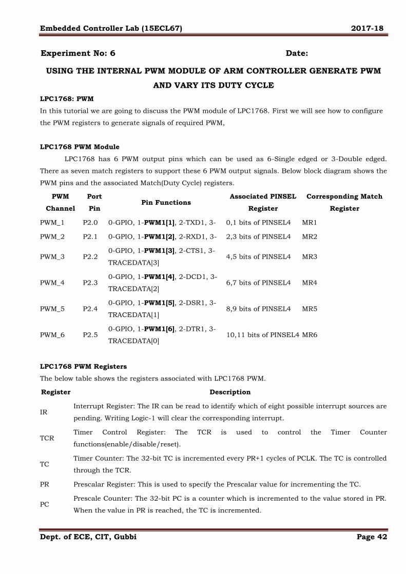
LPC1768 PWM Module
LPC1768 has 6 PWM output pins which can be used as 6-Single edged or 3-Double edged.
There as seven match registers to support these 6 PWM output signals. Below block diagram shows the
PWM pins and the associated Match(Duty Cycle) registers.
PWM
Channel
Port
Pin Pin Functions
Associated PINSEL
Register
Corresponding Match
Register
PWM_1 P2.0 0-GPIO, 1-PWM1[1], 2-TXD1, 3- 0,1 bits of PINSEL4 MR1
PWM_2 P2.1 0-GPIO, 1-PWM1[2], 2-RXD1, 3- 2,3 bits of PINSEL4 MR2
PWM_3 P2.2 0-GPIO, 1-PWM1[3], 2-CTS1, 3-
TRACEDATA[3] 4,5 bits of PINSEL4 MR3
PWM_4 P2.3 0-GPIO, 1-PWM1[4], 2-DCD1, 3-
TRACEDATA[2] 6,7 bits of PINSEL4 MR4
PWM_5 P2.4 0-GPIO, 1-PWM1[5], 2-DSR1, 3-
TRACEDATA[1] 8,9 bits of PINSEL4 MR5
PWM_6 P2.5 0-GPIO, 1-PWM1[6], 2-DTR1, 3-
TRACEDATA[0] 10,11 bits of PINSEL4 MR6
LPC1768 PWM Registers
The below table shows the registers associated with LPC1768 PWM.
Register Description
IR Interrupt Register: The IR can be read to identify which of eight possible interrupt sources are
pending. Writing Logic-1 will clear the corresponding interrupt.
TCR Timer Control Register: The TCR is used to control the Timer Counter
functions(enable/disable/reset).
TC Timer Counter: The 32-bit TC is incremented every PR+1 cycles of PCLK. The TC is controlled
through the TCR.
PR Prescalar Register: This is used to specify the Prescalar value for incrementing the TC.
PC Prescale Counter: The 32-bit PC is a counter which is incremented to the value stored in PR.
When the value in PR is reached, the TC is incremented.

Embedded Controller Lab (15ECL67) 2017-18
Dept. of ECE, CIT, Gubbi Page 43
MCR Match Control Register: The MCR is used to control the reseting of TC and generating of
interrupt whenever a Match occurs.
MR0 Match Register: This register hold the max cycle Time(Ton+Toff).
MR1-
MR6
Match Registers: These registers holds the Match value(PWM Duty) for corresponding PWM
channels(PWM1-PWM6).
PCR PWM Control Register: PWM Control Register. Enables PWM outputs and selects PWM
channel types as either single edge or double edge controlled.
LER Load Enable Register: Enables use of new PWM values once the match occurs.
Register Configuration
The below table shows the registers associated with LPC1768 PWM.
TCR
31:4 3 2 1 0
Reserved PWM Enable Reserved Counter Reset Counter Enable
Bit 0 – Counter Enable
This bit is used to Enable or Disable the PWM Timer and PWM Prescalar Counters
0- Disable the Counters
1- Enable the Counter incrementing.
Bit 1 – Counter reset
This bit is used to clear the PWM Timer and PWM Prescalar Counter values.
0- Do not Clear.
1- The PWM Timer Counter and the PWM Prescale Counter are synchronously reset on the next
positive edge of PCLK.
Bit 3 – PWM Enable
Used to Enable or Disable the PWM Block.
0- PWM Disabled
1- PWM Enabled
MCR
31:21 20 19 18 - 5 4 3 2 1 0
Reserve
d
PWMMR6
S
PWMMR6
R
PWMMR
6I -
PWMMR1
S
PWMMR1
R
PWMMR
1I
PWMMR0
S
PWMMR0
R
PWMMR
0I
PWMMRxI
This bit is used to Enable or Disable the PWM interrupts when the PWMTC matches PWMMRx (x:0-6)
0- Disable the PWM Match interrupt
1- Enable the PWM Match interrupt.

Embedded Controller Lab (15ECL67) 2017-18
Dept. of ECE, CIT, Gubbi Page 44
PWMMRxR
This bit is used to Reset PWMTC whenever it Matches PWMRx(x:0-6)
0- Do not Clear.
1- Reset the PWMTC counter value whenever it matches PWMRx.
PWMMRxS
This bit is used to Stop the PWMTC,PWMPC whenever the PWMTC matches PWMMRx(x:0-6).
0- Disable the PWM stop o match feature
1- Enable the PWM Stop feature. This will stop the PWM whenever the PWMTC reaches the Match
register value.
PCR
31:15 14-9 8-7 6-2 1-0
Unused PWMENA6-PWMENA1 Unused PWMSEL6-PWMSEL2 Unused
PWMSELx
This bit is used to select the single edged and double edge mode form PWMx (x:2-6)
0- Single Edge mode for PWMx
1- Double Edge Mode for PWMx.
PWMENAx
This bit is used to enable/disable the PWM output for PWMx(x:1-6)
0- PWMx Disable.
1- PWMx Enabled.
LER
31-7 6 5 4 3 2 1 0
Unused LEN6 LEN5 LEN4 LEN3 LEN2 LEN1 LEN0
LENx
This bit is used Enable/Disable the loading of new Match value whenever the PWMTC is reset(x:0-6)
PWMTC will be continously incrementing whenever it reaches the PWMMRO, timer will be reset
depeding on PWMTCR configuraion. Once the Timer is reset the New Match values will be loaded from
MR0-MR6 depending on bits set in this register.
0- Disable the loading of new Match Values
1- Load the new Match values from MRx when the timer is reset.

Embedded Controller Lab (15ECL67) 2017-18
Dept. of ECE, CIT, Gubbi Page 45
PWM Working
After looking into the PWM registers, its time to see how the LPC1768 PWM module works.
The TC is continuously incremented and once it matches the MR1(Duty Cycle) the PWM pin is pulled
Low. TC still continues to increment and once it reaches the Cycle time(Ton+Toff) the PWM module
does the following things:
Reset the TC value.
Pull the PWM pin High.
Loads the new Match register values.
Steps to Configure PWM
1. Configure the GPIO pins for PWM operation in respective PINSEL register.
2. Configure TCR to enable the Counter for incrementing the TC, and Enable the PWM block.
3. Set the required pre-scalar value in PR. In our case it will be zero.
4. Configure MCR to reset the TC whenever it matches MR0.
5. Update the Cycle time in MR0. In our case it will be 100.
6. Load the Duty cycles for required PWMx channels in respective match registers MRx(x: 1-6).
7. Enable the bits in LER register to load and latch the new match values.
8. Enable the required pwm channels in PCR register.

Embedded Controller Lab (15ECL67) 2017-18
Dept. of ECE, CIT, Gubbi Page 46
Result:
Embedded Controller Lab (15ECL67) 2017-18
Dept. of ECE, CIT, Gubbi Page 47
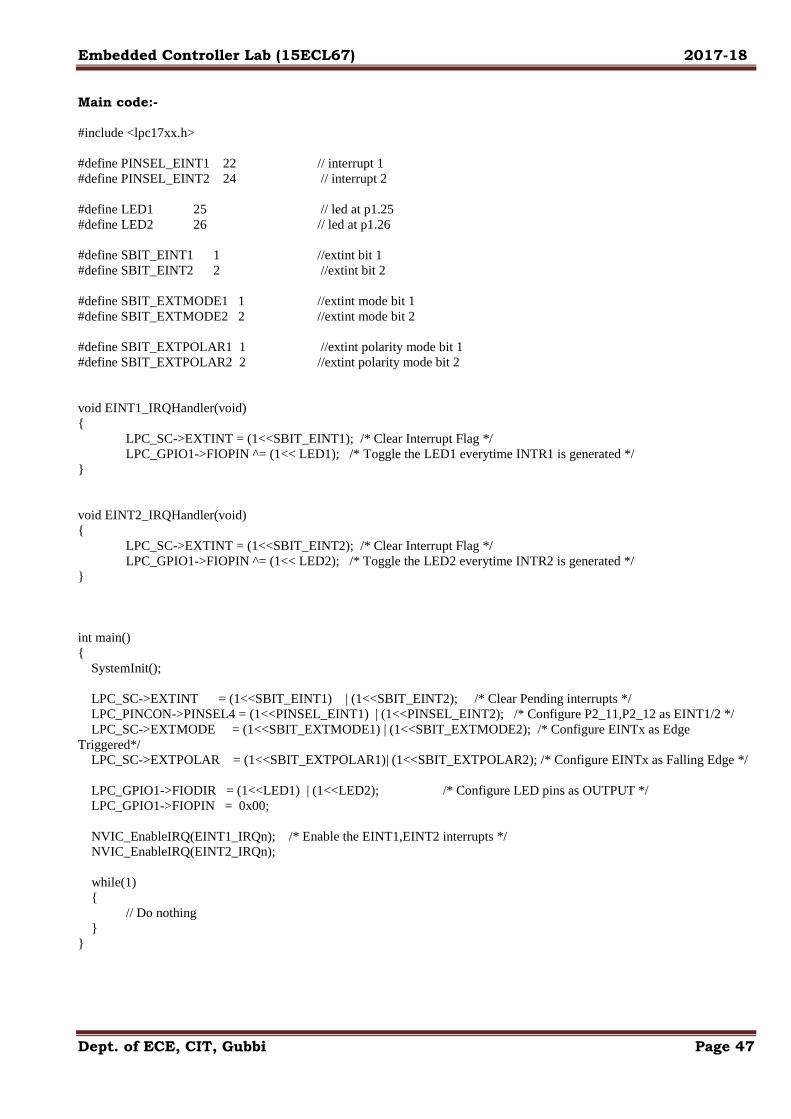
Main code:-
#include <lpc17xx.h>
#define PINSEL_EINT1 22 // interrupt 1
#define PINSEL_EINT2 24 // interrupt 2
#define LED1 25 // led at p1.25
#define LED2 26 // led at p1.26
#define SBIT_EINT1 1 //extint bit 1
#define SBIT_EINT2 2 //extint bit 2
#define SBIT_EXTMODE1 1 //extint mode bit 1
#define SBIT_EXTMODE2 2 //extint mode bit 2
#define SBIT_EXTPOLAR1 1 //extint polarity mode bit 1
#define SBIT_EXTPOLAR2 2 //extint polarity mode bit 2
void EINT1_IRQHandler(void)
{
LPC_SC->EXTINT = (1<<SBIT_EINT1); /* Clear Interrupt Flag */
LPC_GPIO1->FIOPIN ^= (1<< LED1); /* Toggle the LED1 everytime INTR1 is generated */
}
void EINT2_IRQHandler(void)
{
LPC_SC->EXTINT = (1<<SBIT_EINT2); /* Clear Interrupt Flag */
LPC_GPIO1->FIOPIN ^= (1<< LED2); /* Toggle the LED2 everytime INTR2 is generated */
}
int main()
{
SystemInit();
LPC_SC->EXTINT = (1<<SBIT_EINT1) | (1<<SBIT_EINT2); /* Clear Pending interrupts */
LPC_PINCON->PINSEL4 = (1<<PINSEL_EINT1) | (1<<PINSEL_EINT2); /* Configure P2_11,P2_12 as EINT1/2 */
LPC_SC->EXTMODE = (1<<SBIT_EXTMODE1) | (1<<SBIT_EXTMODE2); /* Configure EINTx as Edge
Triggered*/
LPC_SC->EXTPOLAR = (1<<SBIT_EXTPOLAR1)| (1<<SBIT_EXTPOLAR2); /* Configure EINTx as Falling Edge */
LPC_GPIO1->FIODIR = (1<<LED1) | (1<<LED2); /* Configure LED pins as OUTPUT */
LPC_GPIO1->FIOPIN = 0x00;
NVIC_EnableIRQ(EINT1_IRQn); /* Enable the EINT1,EINT2 interrupts */
NVIC_EnableIRQ(EINT2_IRQn);
while(1)
{
// Do nothing
}
}

Embedded Controller Lab (15ECL67) 2017-18
Dept. of ECE, CIT, Gubbi Page 48
Experiment No: 7 Date:
DEMONSTRATE THE USE OF AN EXTERNAL INTERRUPT TO TOGGLE AN LED
ON/OFF
LPC1768: External Interrupts
In this tutorial we will discuss how to configure and use the LPC1768 external interrupts(EINT0-
EINT3).
EINTx Pins
LPC1768 has four external interrupts EINT0-EINT3. As LPC1768 pins are multi functional, these four
interrupts are available on multiple pins.
Below table shows mapping of EINTx pins.
Port Pin PINSEL_FUNC_0 PINSEL_FUNC_1 PINSEL_FUNC_2 PINSEL_FUNC_3
P2.10 GPIO EINT0 NMI
P2.11 GPIO EINT1 I2STX_CLK
P2_12 GPIO EINT2 I2STX_WS
P2.13 GPIO EINT3 I2STX_SDA
EINT Registers
Below table shows the registers associated with LPC1768 external interrupts.
Register Description
PINSELx To configure the pins as External Interrupts
EXTINT External Interrupt Flag Register contains interrupt flags for EINT0,EINT1, EINT2 & EINT3.
EXTMODE External Interrupt Mode register(Level/Edge Triggered)
EXTPOLAR External Interrupt Polarity(Falling/Rising Edge, Active Low/High)

Embedded Controller Lab (15ECL67) 2017-18
Dept. of ECE, CIT, Gubbi Page 49
EXTINT
31:4 3 2 1 0
RESERVED EINT3 EINT2 EINT1 EINT0
EINTx: Bits will be set whenever the interrupt is detected on the particular interrupt pin.
If the interrupts are enabled then the control goes to ISR.
Writing one to specific bit will clear the corresponding interrupt.
EXTMODE
31:4 3 2 1 0
RESERVED EXTMODE3 EXTMODE2 EXTMODE1 EXTMODE0
EXTMODEx: This bits is used to select whether the EINTx pin is level or edge Triggered
0: EINTx is Level Triggered.
1: EINTx is Edge Triggered.
EXTPOLAR
31:4 3 2 1 0
RESERVED EXTPOLAR3 EXTPOLAR2 EXTPOLAR1 EXTPOLAR0
EXTPOLARx: This bits is used to select polarity(LOW/HIGH, FALLING/RISING) of the EINTx interrupt
depending on the EXTMODE register.
0: EINTx is Active Low or Falling Edge (depending on EXTMODEx).
1: EINTx is Active High or Rising Edge (depending on EXTMODEx).
Steps to Configure Interrupts
1. Configure the pins as external interrupts in PINSELx register.
2. Clear any pending interrupts in EXTINT.
3. Configure the EINTx as Edge/Level triggered in EXTMODE register.
4. Select the polarity(Falling/Rising Edge, Active Low/High) of the interrupt in EXTPOLAR register.
5. Finally enable the interrupts by calling NVIC_EnableIRQ() with IRQ number.

Embedded Controller Lab (15ECL67) 2017-18
Dept. of ECE, CIT, Gubbi Page 50
Result:
Embedded Controller Lab (15ECL67) 2017-18
Dept. of ECE, CIT, Gubbi Page 51
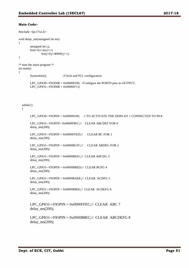
Main Code:-
#include <lpc17xx.h>
void delay_ms(unsigned int ms)
{
unsigned int i,j;
for(i=0;i<ms;i++)
for(j=0;j<40000;j++);
}
/* start the main program */
int main()
{
SystemInit(); //Clock and PLL configuration
LPC_GPIO0->FIODIR = 0x00000100; //Configure the PORT0 pins as OUTPUT;
LPC_GPIO1->FIODIR = 0x00004713;
while(1)
{
LPC_GPIO0->FIOPIN = 0x00000100; // TO ACTIVATE THE DISPLAY 1 CONNECTED TO P0.8
LPC_GPIO1->FIOPIN= 0x0000F8EC;// CLEAR ABCDEF FOR 0
delay_ms(200);
LPC_GPIO1->FIOPIN = 0x0000FFED;// CLEAR BC FOR 1
delay_ms(200);
LPC_GPIO1->FIOPIN = 0x0000BCFC;// CLEAR ABDEG FOR 2
delay_ms(200);
LPC_GPIO1->FIOPIN = 0x0000BEEC;// CLEAR ABCDG 3
delay_ms(200);
LPC_GPIO1->FIOPIN = 0x0000BBED;// CLEAR BCFG 4
delay_ms(200);
LPC_GPIO1->FIOPIN = 0x0000BAEE;// CLEAR ACDFG 5
delay_ms(200);
LPC_GPIO1->FIOPIN = 0x0000B8EE;// CLEAR ACDEFG 6
delay_ms(200);
LPC_GPIO1->FIOPIN = 0x0000FFEC;// CLEAR ABC 7
delay_ms(200);
LPC_GPIO1->FIOPIN = 0x0000B8EC;// CLEAR ABCDEFG 8
delay_ms(200);
Embedded Controller Lab (15ECL67) 2017-18
Dept. of ECE, CIT, Gubbi Page 52
Experiment No: 8 Date:
DISPLAY THE HEX DIGITS 0 TO F ON A 7-SEGMENT LED INTERFACE, WITH AN
APPROPRIATE DELAY IN BETWEEN
7-segment Display
The 7-segment display, also written as “seven segment display”, consists of seven LEDs (hence
its name) arranged in a rectangular fashion as shown. Each of the seven LEDs is called a segment
because when illuminated the segment forms part of a numerical digit (both Decimal and Hex) to be
displayed. An additional 8th LED is sometimes used within the same package thus allowing the
indication of a decimal point, (DP) when two or more 7-segment displays are connected together to
display numbers greater than ten.
Each one of the seven LEDs in the display is given a positional segment with one of its
connection pins being brought straight out of the rectangular plastic package. These individually LED
pins are labelled from a through to g representing each individual LED. The other LED pins are
connected together and wired to form a common pin.
So by forward biasing the appropriate pins of the LED segments in a particular order, some
segments will be light and others will be dark allowing the desired character pattern of the number to
be generated on the display. This then allows us to display each of the ten decimal digits 0 through to 9
on the same 7-segment display.
The displays common pin is generally used to identify which type of 7-segment display it is. As
each LED has two connecting pins, one called the “Anode” and the other called the “Cathode”, there are
therefore two types of LED 7-segment display called: Common Cathode (CC) and Common Anode
(CA).
The difference between the two displays, as their name suggests, is that the common cathode
has all the cathodes of the 7-segments connected directly together and the common anode has all the
anodes of the 7-segments connected together and is illuminated as follows.
The Common Cathode (CC) – In the common cathode display, all the cathode connections of the
LED segments are joined together to logic “0” or ground. The individual segments are
illuminated by application of a “HIGH”, or logic “1” signal via a current limiting resistor to
forward bias the individual Anode terminals (a-g).

Embedded Controller Lab (15ECL67) 2017-18
Dept. of ECE, CIT, Gubbi Page 53
LPC_GPIO1->FIOPIN = 0x0000BAEC;// CLEAR ABCDFG 9
delay_ms(200);
LPC_GPIO1->FIOPIN = 0x0000B9EC;// CLEAR ABCFG A
delay_ms(200);
LPC_GPIO1->FIOPIN = 0x0000B8EF;// CLEAR CDEFG b
delay_ms(200);
LPC_GPIO1->FIOPIN = 0x0000F8FE;// CLEAR ADEF C
delay_ms(200);
LPC_GPIO1->FIOPIN = 0x0000BCED;// CLEAR BCDEG d
delay_ms(200);
LPC_GPIO1->FIOPIN = 0x0000B8FE;// CLEAR ADEFG E
delay_ms(200);
LPC_GPIO1->FIOPIN = 0x0000B9FE;// CLEAR AEFG F
delay_ms(200);
}
}

Embedded Controller Lab (15ECL67) 2017-18
Dept. of ECE, CIT, Gubbi Page 54
Common Cathode 7-segment Display
The Common Anode (CA) – In the common anode display, all the anode connections of the LED
segments are joined together to logic “1”. The individual segments are illuminated by applying a
ground, logic “0” or “LOW” signal via a suitable current limiting resistor to the Cathode of the
particular segment (a-g).
Common Anode 7-segment Display
In general, common anode displays are more popular as many logic circuits can sink more current
than they can source. Also note that a common cathode display is not a direct replacement in a circuit
for a common anode display and vice versa, as it is the same as connecting the LEDs in reverse, and
hence light emission will not take place.
Depending upon the decimal digit to be displayed, the particular set of LEDs is forward biased. For
instance, to display the numerical digit 0, we will need to light up six of the LED segments
corresponding to a, b, c, d, e and f. Thus the various digits from 0 through 9 can be displayed using a
7-segment display as shown.
7-Segment Display Segments for all Numbers
Embedded Controller Lab (15ECL67) 2017-18
Dept. of ECE, CIT, Gubbi Page 55
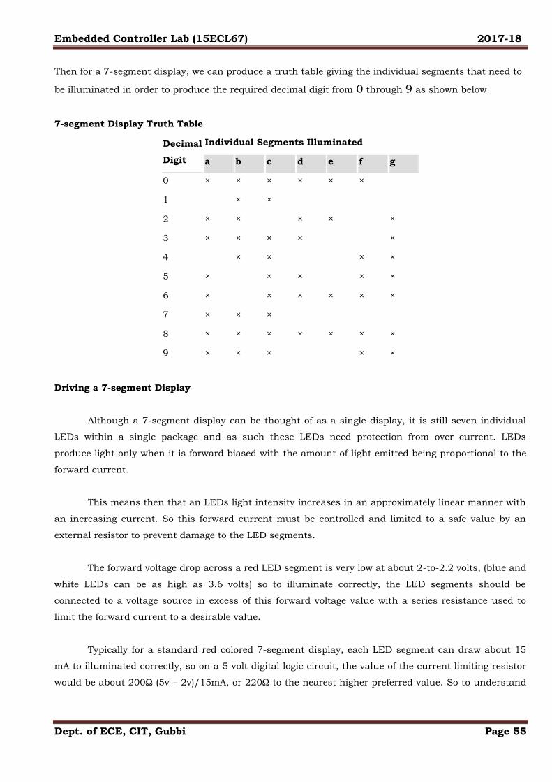
Then for a 7-segment display, we can produce a truth table giving the individual segments that need to
be illuminated in order to produce the required decimal digit from 0 through 9 as shown below.
7-segment Display Truth Table
Decimal
Digit
Individual Segments Illuminated
a b c d e f g
0 × × × × × ×
1 × ×
2 × × × × ×
3 × × × × ×
4 × × × ×
5 × × × × ×
6 × × × × × ×
7 × × ×
8 × × × × × × ×
9 × × × × ×
Driving a 7-segment Display
Although a 7-segment display can be thought of as a single display, it is still seven individual
LEDs within a single package and as such these LEDs need protection from over current. LEDs
produce light only when it is forward biased with the amount of light emitted being proportional to the
forward current.
This means then that an LEDs light intensity increases in an approximately linear manner with
an increasing current. So this forward current must be controlled and limited to a safe value by an
external resistor to prevent damage to the LED segments.
The forward voltage drop across a red LED segment is very low at about 2-to-2.2 volts, (blue and
white LEDs can be as high as 3.6 volts) so to illuminate correctly, the LED segments should be
connected to a voltage source in excess of this forward voltage value with a series resistance used to
limit the forward current to a desirable value.
Typically for a standard red colored 7-segment display, each LED segment can draw about 15
mA to illuminated correctly, so on a 5 volt digital logic circuit, the value of the current limiting resistor
would be about 200Ω (5v – 2v)/15mA, or 220Ω to the nearest higher preferred value. So to understand
Embedded Controller Lab (15ECL67) 2017-18
Dept. of ECE, CIT, Gubbi Page 56
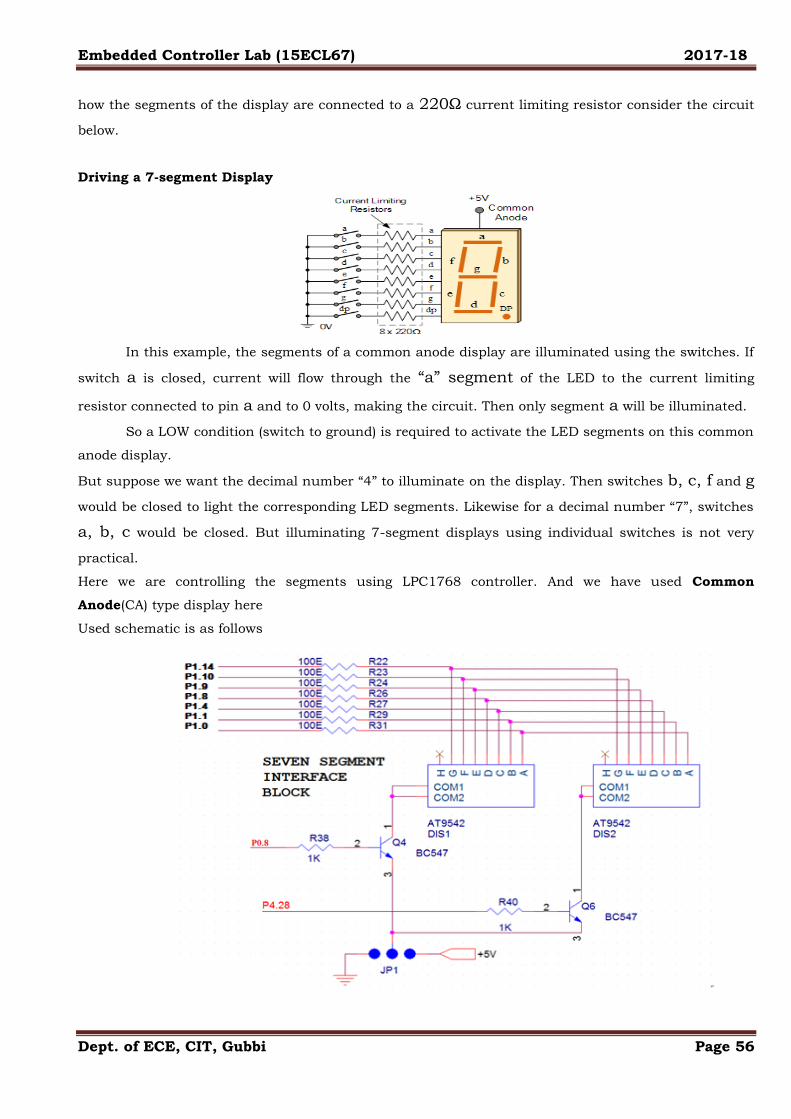
how the segments of the display are connected to a 220Ω current limiting resistor consider the circuit
below.
Driving a 7-segment Display
In this example, the segments of a common anode display are illuminated using the switches. If
switch a is closed, current will flow through the “a” segment of the LED to the current limiting
resistor connected to pin a and to 0 volts, making the circuit. Then only segment a will be illuminated.
So a LOW condition (switch to ground) is required to activate the LED segments on this common
anode display.
But suppose we want the decimal number “4” to illuminate on the display. Then switches b, c, f and g
would be closed to light the corresponding LED segments. Likewise for a decimal number “7”, switches
a, b, c would be closed. But illuminating 7-segment displays using individual switches is not very
practical.
Here we are controlling the segments using LPC1768 controller. And we have used Common
Anode(CA) type display here
Used schematic is as follows

Embedded Controller Lab (15ECL67) 2017-18
Dept. of ECE, CIT, Gubbi Page 57
For illuminate a digit we have to make a appropriate port Low (send 0).
Here 1st make P0.8 or P4.28 High. It will send control active signal to segment. Then initially make
P1.0,P1.1,P1.4,P1.8,P1.9,P1.10,P1.14 all high. Now all the digits become off. Then make
respected segment low by sending CLR signal to GPIO. This cause the segment to illuminate.
Embedded Controller Lab (15ECL67) 2017-18
Dept. of ECE, CIT, Gubbi Page 58
Result:

Embedded Controller Lab (15ECL67) 2017-18
Dept. of ECE, CIT, Gubbi Page 59
Main code:-
#include <lpc17xx.h>
#define SwitchPinNumber 11// port P2.11 connected to switch
#define LedPinNumber 19 //port 1.19-p1.26 connected to 8 leds
#define relayPinNumber 28 //port P1.28 connected to relay
#define buzzerPinNumber 27 //port P1.27 connected to buzzer
int main (void)
{
uint32_t switchStatus;
LPC_GPIO1->FIODIR = 0x1ff80000; /* P1.xx defined as Outputs */
LPC_GPIO1->FIOCLR = 0x1ff80000; /* turn off all the LEDs&relay&buzzer */
LPC_GPIO2->FIODIR = 0x00000000; /* P2.xx defined as input */
while(1)
{
/* Turn On all the leds and wait for one second */
switchStatus = (LPC_GPIO2->FIOPIN>>SwitchPinNumber) & 0x01 ; // Read the switch status
if(switchStatus == 0) //if switch pressed
{
LPC_GPIO1->FIOPIN = (1<<buzzerPinNumber)|(1<<relayPinNumber)|(1<<LedPinNumber); //turn on led,relay and
buzzer
}
else //if switch released
{
LPC_GPIO1->FIOPIN = (0<<buzzerPinNumber)|(0<<relayPinNumber)|(0<<LedPinNumber);
//if switch released led,relay,buzzer off
}
}
}

Embedded Controller Lab (15ECL67) 2017-18
Dept. of ECE, CIT, Gubbi Page 60
Experiment No: 9 Date:
INTERFACE A SIMPLE SWITCH AND DISPLAY ITS STATUS THROUGH RELAY,
BUZZER AND LED
LPC1768: Read Switch status
This is second tutorial on LPC1768 where we are going to read the switches and turn ON/OFF the
LEDs accordingly. LPC1768 has its GPIOs divided into five ports PORT0 - PORT4, although many of
them are not physically 32bit wide. Refer the data sheet for more info.
Register Configuration
The Below registers will be used for Configuring and using the GPIOs registers for sending and
receiving the Digital signals.
PINSEL: GPIO Pins Select Register
Almost all the LPC1768 pins are multiplexed to support more than 1 function. Every GPIO pin has a
minimum of one function and max of four functions. The required function can be selected by
configuring the PINSEL register. As there can be up to 4 functions associated with a GPIO pin, two bits
for each pin are available to select the function. This implies that we need two PINSEL registers to
configure a PORT pins. By this the first 16(P0.0-P0.16) pin functions of PORT0 can be selected by 32
bits of PINSELO register. The remaining 16 bits(P0.16-P0.32) are configured using 32bits of PINSEL1
register. As mentioned earlier every pin has max of four functions. Below table shows how to select the
function for a particular pin using two bits of the PINSEL register.
Value Function Enumeration
00 Primary (default) function, typically GPIO port PINSEL_FUNC_0
01 First alternate function PINSEL_FUNC_1
10 Second alternate function PINSEL_FUNC_2
11 Third alternate function PINSEL_FUNC_3
FIODIR:Fast GPIO Direction Control Register.
This register individually controls the direction of each port pin.
Values Direction
0 Input
1 Output
FIOSET:Fast Port Output Set Register.
This register controls the state of output pins. Writing 1s produces highs at the corresponding port

Embedded Controller Lab (15ECL67) 2017-18
Dept. of ECE, CIT, Gubbi Page 61
pins. Writing 0s has no effect. Reading this register returns the current contents of the port output
register not the physical port value.
Values FIOSET
0 No Effect
1 Sets High on Pin
FIOCLR:
Fast Port Output Clear Register. This register controls the state of output pins. Writing 1s produces
lows at the corresponding port pins. Writing 0s has no effect.
Values FIOCLR
0 No Effect
1 Sets Low on Pin
FIOPIN:
Fast Port Pin Value Register. This register is used for both reading and writing data from/to the PORT.
Output: Writing to this register places corresponding values in all bits of the particular PORT pins.
Input: The current state of digital port pins can be read from this register, regardless of pin direction or
alternate function selection (as long as pins are not configured as an input to ADC).
Note:It is recommended to configure the PORT direction and pin function before using it.
Here switch is pulled up to +3.3 volt. So when pressed port should read active low
signal(0),normal condition is active high(1).

Embedded Controller Lab (15ECL67) 2017-18
Dept. of ECE, CIT, Gubbi Page 62
Result:
Embedded Controller Lab (15ECL67) 2017-18
Dept. of ECE, CIT, Gubbi Page 63
Main code:-
#include <LPC17xx.H>
#include <stdint.h>
#include <stdio.h>
#include "delay.h"
#include "spi_manul.h"
#include "lcd.h"
#define pulse_val 2
main()
{
unsigned int spi_rsv=0;
float vin;
char buf[20];
SystemInit ();
lcd_init();
lcd_str("SPI 3202-b");
delay(60000);
delay(60000);
while(1)
{
lcd_clr();
lcd_cmd(0x80);
spi_rsv = spi_data1(15);
vin = ( ( spi_rsv & 0xfff ) * (3.3) ) / 4096 ;
sprintf(buf,"Temp: %0.2f degC",(vin*100) );
lcd_str(buf);
delay(50000);
delay(50000);
}
}
SPI ADC data fetching program:-
#include <LPC17xx.H>
#include "delay.h"
#define pulse_val 2
#define CLK 1<<27
#define CS 1<<28
#define DDOUT 26
#define DOUT 1<<25
#define DIN 1<<26
#define spi_stst 0
unsigned int spi_data(char sel)
{
char clks = 4;
LPC_GPIO0->FIODIR |= CS|CLK;
LPC_GPIO3->FIODIR = DOUT;
LPC_GPIO0->FIOSET = CS|CLK;
LPC_GPIO3->FIOCLR = DOUT;
nop_delay(100);
#if spi_stst
if ( LPC_GPIO3->FIOPIN & DIN )
{
return 'P';
}
#endif
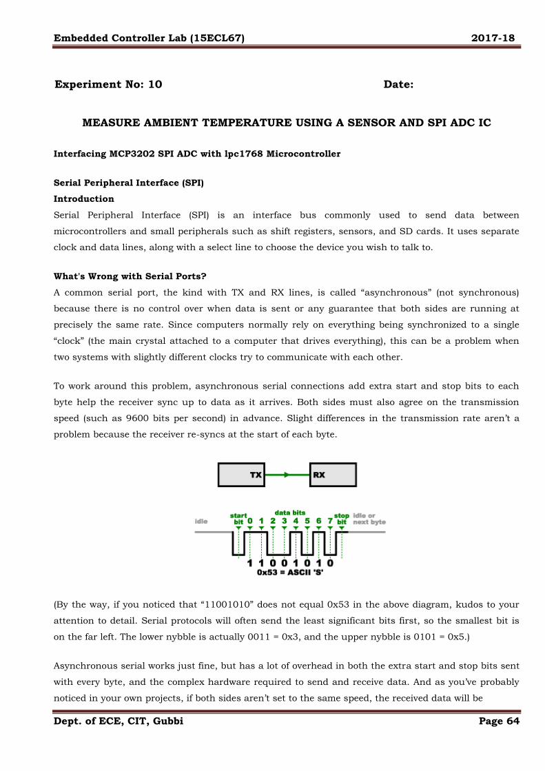
Embedded Controller Lab (15ECL67) 2017-18
Dept. of ECE, CIT, Gubbi Page 64
Experiment No: 10 Date:
MEASURE AMBIENT TEMPERATURE USING A SENSOR AND SPI ADC IC
Interfacing MCP3202 SPI ADC with lpc1768 Microcontroller
Serial Peripheral Interface (SPI)
Introduction
Serial Peripheral Interface (SPI) is an interface bus commonly used to send data between
microcontrollers and small peripherals such as shift registers, sensors, and SD cards. It uses separate
clock and data lines, along with a select line to choose the device you wish to talk to.
What's Wrong with Serial Ports?
A common serial port, the kind with TX and RX lines, is called “asynchronous” (not synchronous)
because there is no control over when data is sent or any guarantee that both sides are running at
precisely the same rate. Since computers normally rely on everything being synchronized to a single
“clock” (the main crystal attached to a computer that drives everything), this can be a problem when
two systems with slightly different clocks try to communicate with each other.
To work around this problem, asynchronous serial connections add extra start and stop bits to each
byte help the receiver sync up to data as it arrives. Both sides must also agree on the transmission
speed (such as 9600 bits per second) in advance. Slight differences in the transmission rate aren‟t a
problem because the receiver re-syncs at the start of each byte.
(By the way, if you noticed that “11001010” does not equal 0x53 in the above diagram, kudos to your
attention to detail. Serial protocols will often send the least significant bits first, so the smallest bit is
on the far left. The lower nybble is actually 0011 = 0x3, and the upper nybble is 0101 = 0x5.)
Asynchronous serial works just fine, but has a lot of overhead in both the extra start and stop bits sent
with every byte, and the complex hardware required to send and receive data. And as you‟ve probably
noticed in your own projects, if both sides aren‟t set to the same speed, the received data will be

Embedded Controller Lab (15ECL67) 2017-18
Dept. of ECE, CIT, Gubbi Page 65
LPC_GPIO0->FIOCLR = CS;
nop_delay(pulse_val);
while(clks)
{
LPC_GPIO0->FIOCLR = CLK;
nop_delay(pulse_val);
LPC_GPIO3->FIOPIN = (sel & 1) << DDOUT;
sel = sel >> 1;
LPC_GPIO0->FIOSET = CLK;
nop_delay(pulse_val);
clks--;
}
LPC_GPIO0->FIOCLR = CLK;
nop_delay(pulse_val);
if (!( LPC_GPIO3->FIOPIN & DIN ) )
{
return 'U';
}
clks = 12;
while(clks)
{
clks--;
LPC_GPIO0->FIOCLR = CLK;
nop_delay(pulse_val);
LPC_GPIO0->FIOSET = CLK;
nop_delay(pulse_val);
}
nop_delay(pulse_val);
if (!( LPC_GPIO3->FIOPIN & DIN ) )
{
return 'U';
}
return 'Z';
}
unsigned int spi_data1(char sel)
{
unsigned int spi_reg=0;
char clks = 12;
LPC_GPIO0->FIODIR |= CS|CLK;
LPC_GPIO3->FIODIR = DOUT;
LPC_GPIO0->FIOSET = CS|CLK;
LPC_GPIO3->FIOSET = DOUT;
LPC_GPIO3->FIOPIN = DIN;
nop_delay(100);
LPC_GPIO0->FIOCLR = CS;
//start condition
LPC_GPIO0->FIOCLR = CLK;
LPC_GPIO3->FIOSET = DOUT;
nop_delay(pulse_val);
LPC_GPIO0->FIOSET = CLK;
nop_delay(5);
//single mode
LPC_GPIO0->FIOCLR = CLK;
LPC_GPIO3->FIOSET = DOUT;
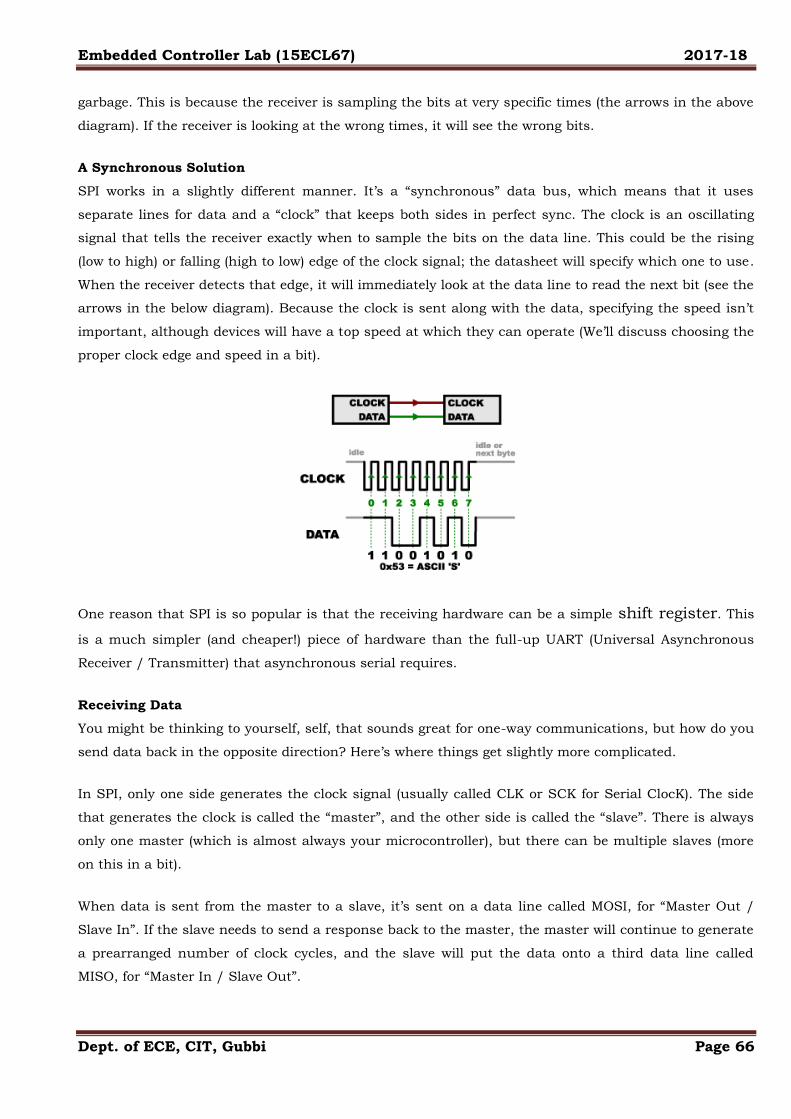
Embedded Controller Lab (15ECL67) 2017-18
Dept. of ECE, CIT, Gubbi Page 66
garbage. This is because the receiver is sampling the bits at very specific times (the arrows in the above
diagram). If the receiver is looking at the wrong times, it will see the wrong bits.
A Synchronous Solution
SPI works in a slightly different manner. It‟s a “synchronous” data bus, which means that it uses
separate lines for data and a “clock” that keeps both sides in perfect sync. The clock is an oscillating
signal that tells the receiver exactly when to sample the bits on the data line. This could be the rising
(low to high) or falling (high to low) edge of the clock signal; the datasheet will specify which one to use.
When the receiver detects that edge, it will immediately look at the data line to read the next bit (see the
arrows in the below diagram). Because the clock is sent along with the data, specifying the speed isn‟t
important, although devices will have a top speed at which they can operate (We‟ll discuss choosing the
proper clock edge and speed in a bit).
One reason that SPI is so popular is that the receiving hardware can be a simple shift register. This
is a much simpler (and cheaper!) piece of hardware than the full-up UART (Universal Asynchronous
Receiver / Transmitter) that asynchronous serial requires.
Receiving Data
You might be thinking to yourself, self, that sounds great for one-way communications, but how do you
send data back in the opposite direction? Here‟s where things get slightly more complicated.
In SPI, only one side generates the clock signal (usually called CLK or SCK for Serial ClocK). The side
that generates the clock is called the “master”, and the other side is called the “slave”. There is always
only one master (which is almost always your microcontroller), but there can be multiple slaves (more
on this in a bit).
When data is sent from the master to a slave, it‟s sent on a data line called MOSI, for “Master Out /
Slave In”. If the slave needs to send a response back to the master, the master will continue to generate
a prearranged number of clock cycles, and the slave will put the data onto a third data line called
MISO, for “Master In / Slave Out”.

Embedded Controller Lab (15ECL67) 2017-18
Dept. of ECE, CIT, Gubbi Page 67
nop_delay(pulse_val);
LPC_GPIO0->FIOSET = CLK;
nop_delay(5);
//chanl 1
LPC_GPIO0->FIOCLR = CLK;
LPC_GPIO3->FIOSET = DOUT;
nop_delay(pulse_val);
LPC_GPIO0->FIOSET = CLK;
nop_delay(5);
//msb first
LPC_GPIO0->FIOCLR = CLK;
LPC_GPIO3->FIOSET = DOUT;
nop_delay(pulse_val);
LPC_GPIO0->FIOSET = CLK;
nop_delay(5);
LPC_GPIO0->FIOCLR = CLK;
nop_delay(pulse_val);
LPC_GPIO0->FIOSET = CLK;
nop_delay(5);
clks = 12;
while(clks)
{
LPC_GPIO0->FIOCLR = CLK;
nop_delay(pulse_val);
LPC_GPIO0->FIOSET = CLK;
if( ( LPC_GPIO3->FIOPIN & DIN ) )
{
spi_reg |= 1<<(clks-1);
}
else
{
spi_reg = spi_reg;
}
clks--;
nop_delay(5);
}
nop_delay(1);
return spi_reg;
}
LCD display program:-
#include <LPC17xx.H>
#include "delay.h"
#define RRW (7<<9)
#define DATA_L (15<<19)
void lcd_pin(void)
{
LPC_GPIO0->FIODIR |= RRW|DATA_L;
}
void lcd_cmd(unsigned char cmd)
{
LPC_GPIO0->FIOPIN =( ( ( cmd & 0xf0 )>> 4) << 19 )| (1<<11);
delay(200);

Embedded Controller Lab (15ECL67) 2017-18
Dept. of ECE, CIT, Gubbi Page 68
Notice we said “prearranged” in the above description. Because the master always generates the clock
signal, it must know in advance when a slave needs to return data and how much data will be
returned. This is very different than asynchronous serial, where random amounts of data can be sent
in either direction at any time. In practice this isn‟t a problem, as SPI is generally used to talk to
sensors that have a very specific command structure. For example, if you send the command for “read
data” to a device, you know that the device will always send you, for example, two bytes in return. (In
cases where you might want to return a variable amount of data, you could always return one or two
bytes specifying the length of the data and then have the master retrieve the full amount.)
Note that SPI is “full duplex” (has separate send and receive lines), and, thus, in certain situations, you
can transmit and receive data at the same time (for example, requesting a new sensor reading while
retrieving the data from the previous one). Your device‟s datasheet will tell you if this is possible.
Slave Select (SS)
There‟s one last line you should be aware of, called SS for Slave Select. This tells the slave that it
should wake up and receive / send data and is also used when multiple slaves are present to select the
one you‟d like to talk to.
Embedded Controller Lab (15ECL67) 2017-18
Dept. of ECE, CIT, Gubbi Page 69
LPC_GPIO0->FIOPIN =( ( ( cmd & 0xf0 )>> 4) << 19 );
LPC_GPIO0->FIOCLR |= RRW|DATA_L;
delay(10);
LPC_GPIO0->FIOPIN = ( ( ( cmd & 0xf ) ) << 19 )| (1<<11);
delay(200);
LPC_GPIO0->FIOPIN = ( ( ( cmd & 0xf ) ) << 19 );
}
void lcd_data(unsigned char cmd)
{
LPC_GPIO0->FIOPIN =(1<<9)|( ( ( cmd & 0xf0 )>> 4) << 19 )| (1<<11);
delay(200);
LPC_GPIO0->FIOPIN =( ( ( cmd & 0xf0 )>> 4) << 19 );
LPC_GPIO0->FIOCLR |= RRW|DATA_L;
delay(10);
LPC_GPIO0->FIOPIN = (1<<9)|( ( ( cmd & 0xf ) ) << 19 )| (1<<11);
delay(200);
LPC_GPIO0->FIOPIN = ( ( ( cmd & 0xf ) ) << 19 );
}
void lcd_init(void)
{
lcd_pin();
lcd_cmd(0x03);
delay(3000);
lcd_cmd(0x03);
delay(1000);
lcd_cmd(0x03);
delay(100);
lcd_cmd(0x2);
lcd_cmd(0x28);
lcd_cmd(0x0e);
lcd_cmd(0x06);
lcd_cmd(0x01);
delay(1);
}
void lcd_str(char *lstr)
{
while(*lstr)
{
lcd_data(*lstr);
lstr++;
}
}
void lcd_clr(void)
{
lcd_cmd(0x03);
delay(10);
lcd_cmd(0x2);
lcd_cmd(0x28);
lcd_cmd(0x0e);
lcd_cmd(0x06);
lcd_cmd(0x01);
delay(10);
}
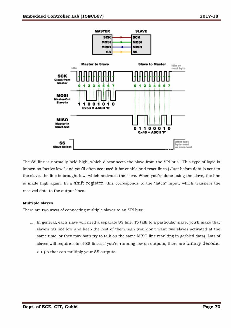
Embedded Controller Lab (15ECL67) 2017-18
Dept. of ECE, CIT, Gubbi Page 70
The SS line is normally held high, which disconnects the slave from the SPI bus. (This type of logic is
known as “active low,” and you‟ll often see used it for enable and reset lines.) Just before data is sent to
the slave, the line is brought low, which activates the slave. When you‟re done using the slave, the line
is made high again. In a shift register, this corresponds to the “latch” input, which transfers the
received data to the output lines.
Multiple slaves
There are two ways of connecting multiple slaves to an SPI bus:
1. In general, each slave will need a separate SS line. To talk to a particular slave, you‟ll make that
slave‟s SS line low and keep the rest of them high (you don‟t want two slaves activated at the
same time, or they may both try to talk on the same MISO line resulting in garbled data). Lots of
slaves will require lots of SS lines; if you‟re running low on outputs, there are binary decoder
chips that can multiply your SS outputs.

Embedded Controller Lab (15ECL67) 2017-18
Dept. of ECE, CIT, Gubbi Page 71
1. On the other hand, some parts prefer to be daisy-chained together, with the MISO (output) of
one going to the MOSI (input) of the next. In this case, a single SS line goes to all the slaves.
Once all the data is sent, the SS line is raised, which causes all the chips to be activated
simultaneously. This is often used for daisy-chained shift registers and addressable LED
drivers.
Note that, for this layout, data overflows from one slave to the next, so to send data to any one slave,
you‟ll need to transmit enough data to reach all of them. Also, keep in mind that the first piece of data
you transmit will end up in the last slave.
This type of layout is typically used in output-only situations, such as driving LEDs where you don‟t
need to receive any data back. In these cases you can leave the master‟s MISO line disconnected.
However, if data does need to be returned to the master, you can do this by closing the daisy-chain loop
(blue wire in the above diagram). Note that if you do this, the return data from slave 1 will need to pass
through all the slaves before getting back to the master, so be sure to send enough receive commands
to get the data you need.

Embedded Controller Lab (15ECL67) 2017-18
Dept. of ECE, CIT, Gubbi Page 72
Programming for SPI
Many microcontrollers have built-in SPI peripherals that handle all the details of sending and receiving
data, and can do so at very high speeds. The SPI protocol is also simple enough that you (yes, you!) can
write your own routines to manipulate the I/O lines in the proper sequence to transfer data. (A good
example is on the Wikipedia SPI page.)
You will need to select some options when setting up your interface. These options must match those of
the device you‟re talking to; check the device‟s datasheet to see what it requires.
Resources and Going Further
Tips and Tricks
Because of the high speed signals, SPI should only be used to send data over short distances
(up to a few feet). If you need to send data further than that, lower the clock speed, and
consider using specialized driver chips.
If things aren‟t working the way you think they should, a logic analyzer is a very helpful tool.
Smart analyzers like the Saleae USB Logic Analyzer can even decode the data bytes for a
display or logging.
Advantages of SPI:
It‟s faster than asynchronous serial
The receive hardware can be a simple shift register
It supports multiple slaves

Embedded Controller Lab (15ECL67) 2017-18
Dept. of ECE, CIT, Gubbi Page 73
Disadvantages of SPI:
It requires more signal lines (wires) than other communications methods
The communications must be well-defined in advance (you can‟t send random amounts of data
whenever you want)
The master must control all communications (slaves can‟t talk directly to each other)
It usually requires separate SS lines to each slave, which can be problematic if numerous slaves
are needed.
ADC (Analog to Digital Converter):
The Microchip Technology Inc. MCP3202 is a successive approximation 12-bit Analog-to-Digital
(A/D) Converter with on-board sample and hold circuitry. The MCP3202 is programmable to provide
a single pseudo-differential input pair or dual single-ended inputs. Differential Nonlinearity (DNL) is
specified at ±1 LSB, and Integral Nonlinearity (INL) is offered in ±1 LSB (MCP3202-B) and ±2 LSB
(MCP3202-C) versions. Communication with the device is done using a simple serial interface
compatible with the SPI protocol. The device is capable of conversion rates of up to 100ksps at 5V and
50ksps at 2.7V.The MCP3202 is a Dual Channel 12-Bit A/D Converter with SPI Serial Interface By
Microchip . In this tutorial i will interface this ADC using lpc1768 microcontroller using SPI Protocol in
mode(0,0) . Maximum clock rate supported by MCP3202 is 1.8 MHz.
Fsample = 100 KSPS
Fclk = 18*Fsample
MCP3202
Pin description and Pin functional table of MCP3202
Configuring SPI Control Register :
Serial Peripheral interface allows high speed synchronous data communication between lpc1768
microcontrollers.
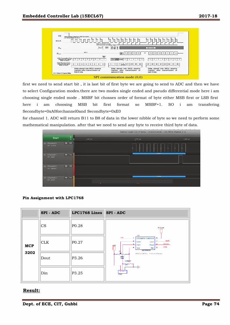
Embedded Controller Lab (15ECL67) 2017-18
Dept. of ECE, CIT, Gubbi Page 74
first we need to send start bit , it is last bit of first byte we are going to send to ADC and then we have
to select Configuration modes.there are two modes single ended and pseudo differential mode here i am
choosing single ended mode . MSBF bit chosses order of format of byte either MSB first or LSB first
here i am choosing MSB bit first format so MSBF=1. SO i am transfering
Secondbyte=0xA0forchannel0and Secondbyte=0xE0
for channel 1. ADC will return B11 to B8 of data in the lower nibble of byte so we need to perform some
mathematical manipulation. after that we need to send any byte to receive third byte of data.
Pin Assignment with LPC1768
SPI - ADC LPC1768 Lines SPI - ADC
MCP
3202
CS P0.28
CLK P0.27
Dout P3.26
Din P3.25
Result:

Embedded Controller Lab (15ECL67) 2017-18
Dept. of ECE, CIT, Gubbi Page 75
Main ADC Code
#include "lpc17xx.h"
#include "lcd.h"
#define VREF 3.3 //Reference Voltage at VREFP pin, given VREFN = 0V(GND)
#define ADC_CLK_EN (1<<12)
#define SEL_AD0_2 (1<<2) //Select Channel AD0.2
#define CLKDIV 1 //ADC clock-divider (ADC_CLOCK=PCLK/CLKDIV+1) = 12.5Mhz @ 25Mhz PCLK
#define PWRUP (1<<21) //setting it to 0 will power it down
#define START_CNV (1<<24) //001 for starting the conversion immediately
#define ADC_DONE (1U<<31) //define it as unsigned value or compiler will throw #61-D warning
#define ADCR_SETUP_SCM ((CLKDIV<<8) | PWRUP)
////////// Init ADC0 CH2 /////////////////
Init_ADC()
{
// Convert Port pin 0.25 to function as AD0.2
LPC_SC->PCONP |= ADC_CLK_EN; //Enable ADC clock
LPC_ADC->ADCR = ADCR_SETUP_SCM | SEL_AD0_2;
LPC_PINCON->PINSEL1 |= (1<<18) ; //select AD0.2 for P0.25
}
////////// READ ADC0 CH:2 /////////////////
unsigned int Read_ADC()
{
unsigned int i=0;
LPC_ADC->ADCR |= START_CNV; //Start new Conversion
while((LPC_ADC->ADDR2 & ADC_DONE) == 0); //Wait untill conversion is finished
i = (LPC_ADC->ADDR2>>4) & 0xFFF; //12 bit Mask to extract result
}
////////// DISPLAY ADC VALUE /////////////////
Display_ADC()
{
unsigned int adc_value = 0;
char buf[4] = {5};
float voltage = 0.0;
adc_value = Read_ADC();
sprintf((char *)buf, "%3d", adc_value); // display 3 decima place
lcd_putstring16(0,"ADC VAL = 000 "); //1st line display
lcd_putstring16(1,"Voltage 00 V"); //2nd line display
lcd_gotoxy(0,10);
lcd_putstring(buf);
voltage = (adc_value * 3.3) / 4095 ;
lcd_gotoxy(1,8);
sprintf(buf, "%3.2f", voltage);
lcd_putstring(buf);
}
////////// MAIN /////////////////
int main (void)
{
init_lcd();
Init_ADC();
lcd_putstring16(0,"** MICROLAB **");
lcd_putstring16(1,"** INSTRUMENTS **");
delay(60000);
delay(60000);
delay(60000);
lcd_putstring16(0,"ADC Value.. ");
lcd_putstring16(1,"voltage.......");
Embedded Controller Lab (15ECL67) 2017-18
Dept. of ECE, CIT, Gubbi Page 76
Additional Programs
DISPLAY DIGITAL OUTPUT FOR GIVEN ANALOG INPUT USING INTERNAL ADC
LPC1768: ADC Programming
In this tutorial we are going to discuss how to use the inbuilt LPC1768 ADC.
Here we will discuss the register associated with ADC and mainly we will focus on basic registers
required for ADC.
The other features like Burst Conversion, accessing different register for each channel, ADC conversion
depending on Timers,ADC Interrupts etc will be out of scope of this tutorial.
Later we will see how to interface a POT,LDR,Temp Sensor(LM35).
Finally we will see how to use the ExploreEmbedded libraries for ADC.
LPC1768 ADC Block
LPC1768 has an inbuilt 12 bit Successive Approximation ADC which is multiplexed among 8 input
pins. The ADC reference voltage is measured across VREFN to VREFP, meaning it can do the
conversion within this range. Usually the VREFP is connected to VDD and VREFN is connected to GND.
As LPC1768 works on 3.3 volts, this will be the ADC reference voltage.
Now the $$resolution of ADC = 3.3/(2^{12}) = 3.3/4096 =0.000805 = 0.8mV$$
The below block diagram shows the ADC input pins multiplexed with other GPIO pins.
The ADC pin can be enabled by configuring the corresponding PINSEL register to select ADC function.
When the ADC function is selected for that pin in the Pin Select register, other Digital signals are
disconnected from the ADC input pins.
Adc Channel Port Pin Pin Functions Associated PINSEL Register
AD0 P0.23 0-GPIO, 1-AD0[0], 2-I2SRX_CLK, 3-CAP3[0] 14,15 bits of PINSEL1
AD1 P0.24 0-GPIO, 1-AD0[1], 2-I2SRX_WS, 3-CAP3[1] 16,17 bits of PINSEL1
AD2 P0.25 0-GPIO, 1-AD0[2], 2-I2SRX_SDA, 3-TXD3 18,19 bits of PINSEL1
AD3 P0.26 0-GPIO, 1-AD0[3], 2-AOUT, 3-RXD3 20,21 bits of PINSEL1
AD4 P1.30 0-GPIO, 1-VBUS, 2- , 3-AD0[4] 28,29 bits of PINSEL3
AD5 P1.31 0-GPIO, 1-SCK1, 2- , 3-AD0[5] 30,31 bits of PINSEL3
AD6 P0.3 0-GPIO, 1-RXD0, 2-AD0[6], 3- 6,7 bits of PINSEL0
AD7 P0.2 0-GPIO, 1-TXD0, 2-AD0[7], 3- 4,5 bits of PINSEL0
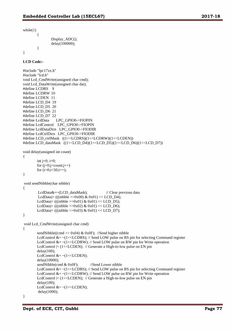
Embedded Controller Lab (15ECL67) 2017-18
Dept. of ECE, CIT, Gubbi Page 77
while(1)
{
Display_ADC();
delay(100000);
}
}
LCD Code:-
#include "lpc17xx.h"
#include "lcd.h"
void Lcd_CmdWrite(unsigned char cmd);
void Lcd_DataWrite(unsigned char dat);
#define LCDRS 9
#define LCDRW 10
#define LCDEN 11
#define LCD_D4 19
#define LCD_D5 20
#define LCD_D6 21
#define LCD_D7 22
#define LcdData LPC_GPIO0->FIOPIN
#define LcdControl LPC_GPIO0->FIOPIN
#define LcdDataDirn LPC_GPIO0->FIODIR
#define LcdCtrlDirn LPC_GPIO0->FIODIR
#define LCD_ctrlMask ((1<<LCDRS)|(1<<LCDRW)|(1<<LCDEN))
#define LCD_dataMask ((1<<LCD_D4)|(1<<LCD_D5)|(1<<LCD_D6)|(1<<LCD_D7))
void delay(unsigned int count)
{
int j=0, i=0;
for (j=0;j<count;j++)
for (i=0;i<50;i++);
}
void sendNibble(char nibble)
{
LcdData&=~(LCD_dataMask); // Clear previous data
LcdData|= (((nibble >>0x00) & 0x01) << LCD_D4);
LcdData|= (((nibble >>0x01) & 0x01) << LCD_D5);
LcdData|= (((nibble >>0x02) & 0x01) << LCD_D6);
LcdData|= (((nibble >>0x03) & 0x01) << LCD_D7);
}
void Lcd_CmdWrite(unsigned char cmd)
{
sendNibble((cmd >> 0x04) & 0x0F); //Send higher nibble
LcdControl &= ~(1<<LCDRS); // Send LOW pulse on RS pin for selecting Command register
LcdControl &= ~(1<<LCDRW); // Send LOW pulse on RW pin for Write operation
LcdControl |= (1<<LCDEN); // Generate a High-to-low pulse on EN pin
delay(100);
LcdControl &= ~(1<<LCDEN);
delay(10000);
sendNibble(cmd & 0x0F); //Send Lower nibble
LcdControl &= ~(1<<LCDRS); // Send LOW pulse on RS pin for selecting Command register
LcdControl &= ~(1<<LCDRW); // Send LOW pulse on RW pin for Write operation
LcdControl |= (1<<LCDEN); // Generate a High-to-low pulse on EN pin
delay(100);
LcdControl &= ~(1<<LCDEN);
delay(1000);
}
Embedded Controller Lab (15ECL67) 2017-18
Dept. of ECE, CIT, Gubbi Page 78
ADC Registers
The below table shows the registers associated with LPC1768 ADC.
We are going to focus only on ADCR and ADGDR as these are sufficient for simple A/D conversion.
However once you are familiar with LPC1768 ADC, you can explore the other features and the
associated registers.
Register Description
ADCR A/D COntrol Register: Used for Configuring the ADC
ADGDR A/D Global Data Register: This register contains the ADC‟s DONE bit and the result of
the most recent A/D conversion
ADINTEN A/D Interrupt Enable Register
ADDR0 -
ADDR7 A/D Channel Data Register: Contains the recent ADC value for respective channel
ADSTAT A/D Status Register: Contains DONE & OVERRUN flag for all the ADC channels
ADC Register Configuration
Now lets see how to configure the individual registers for ADC conversion.
ADCR
31:28 27 26:24 23:22 21 20:17 16 15:8 7:0
Reserved EDGE START Reserved PDN Reserved BURST CLCKDIV SEL
Bit 7:0 – SEL : Channel Select
These bits are used to select a particular channel for ADC conversion. One bit is allotted for each
channel. Setting the Bit-0 will make the ADC to sample AD0[0] for conversion. Similary setting bit-7
will do the conversion for AD0[7].
Bit 15:8 – CLCKDIV : Clock Divisor
The APB clock (PCLK_ADC0) is divided by (this value plus one) to produce the clock for the A/D
converter, which should be less than or equal to 13 MHz.
Bit 16 – BURST
This bit is used for BURST conversion. If this bit is set the ADC module will do the conversion for all
the channels that are selected(SET) in SEL bits.
CLearing this bit will disable the BURST conversion.
Bit 21 – PDN : Power Down Mode
Setting this bit brings ADC out of power down mode and makes it operational.
Clearing this bit will power down the ADC.
Embedded Controller Lab (15ECL67) 2017-18
Dept. of ECE, CIT, Gubbi Page 79
void Lcd_DataWrite(unsigned char dat)
{
sendNibble((dat >> 0x04) & 0x0F); //Send higher nibble
LcdControl |= (1<<LCDRS); // Send HIGH pulse on RS pin for selecting data register
LcdControl &= ~(1<<LCDRW); // Send LOW pulse on RW pin for Write operation
LcdControl |= (1<<LCDEN); // Generate a High-to-low pulse on EN pin
delay(100);
LcdControl &= ~(1<<LCDEN);
delay(1000);
sendNibble(dat & 0x0F); //Send Lower nibble
LcdControl |= (1<<LCDRS); // Send HIGH pulse on RS pin for selecting data register
LcdControl &= ~(1<<LCDRW); // Send LOW pulse on RW pin for Write operation
LcdControl |= (1<<LCDEN); // Generate a High-to-low pulse on EN pin
delay(100);
LcdControl &= ~(1<<LCDEN);
delay(1000);
}
void lcd_clear( void)
{
Lcd_CmdWrite( 0x01 );
}
int lcd_gotoxy( unsigned char x, unsigned char y)
{
unsigned char retval = TRUE;
if( (x > 1) && (y > 15) )
{
retval = FALSE;
}
else
{
if( x == 0 ) Lcd_CmdWrite( 0x80 + y ); //Move the cursor to beginning of the first line
else if( x==1 ) Lcd_CmdWrite( 0xC0 + y );// Move the cursor to beginning of the second line
}
return retval;
}
void lcd_putchar( unsigned char c )
{
Lcd_DataWrite( c );
}
void lcd_putstring( char *string )
{
while(*string != '\0')
{
lcd_putchar( *string );
string++;
}
}
void lcd_putstring16( unsigned char line, char *string )
{
unsigned char len = 16;
lcd_gotoxy( line, 0 );
while(*string != '\0' && len--)
{
lcd_putchar( *string );
string++;
}
}
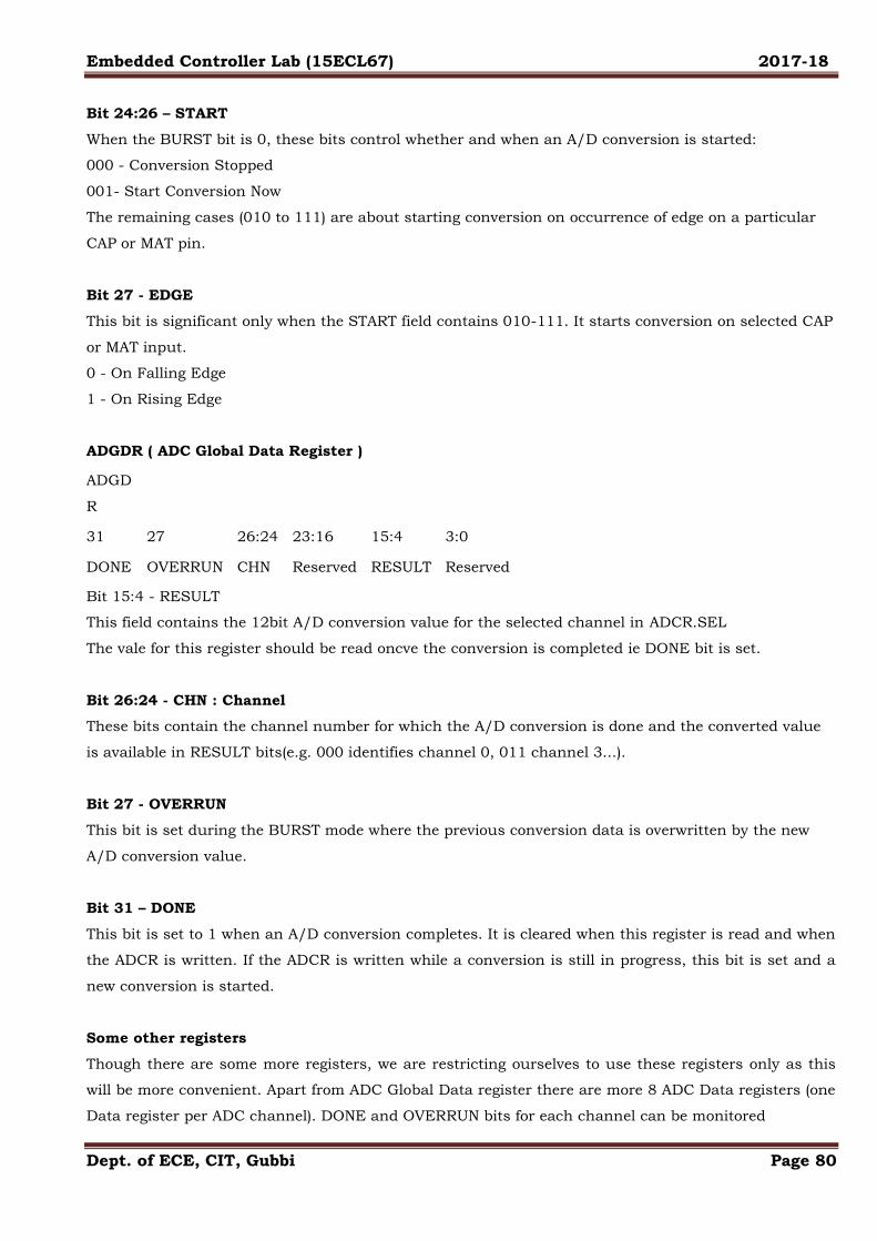
Embedded Controller Lab (15ECL67) 2017-18
Dept. of ECE, CIT, Gubbi Page 80
Bit 24:26 – START
When the BURST bit is 0, these bits control whether and when an A/D conversion is started:
000 - Conversion Stopped
001- Start Conversion Now
The remaining cases (010 to 111) are about starting conversion on occurrence of edge on a particular
CAP or MAT pin.
Bit 27 - EDGE
This bit is significant only when the START field contains 010-111. It starts conversion on selected CAP
or MAT input.
0 - On Falling Edge
1 - On Rising Edge
ADGDR ( ADC Global Data Register )
ADGD
R
31 27 26:24 23:16 15:4 3:0
DONE OVERRUN CHN Reserved RESULT Reserved
Bit 15:4 - RESULT
This field contains the 12bit A/D conversion value for the selected channel in ADCR.SEL
The vale for this register should be read oncve the conversion is completed ie DONE bit is set.
Bit 26:24 - CHN : Channel
These bits contain the channel number for which the A/D conversion is done and the converted value
is available in RESULT bits(e.g. 000 identifies channel 0, 011 channel 3...).
Bit 27 - OVERRUN
This bit is set during the BURST mode where the previous conversion data is overwritten by the new
A/D conversion value.
Bit 31 – DONE
This bit is set to 1 when an A/D conversion completes. It is cleared when this register is read and when
the ADCR is written. If the ADCR is written while a conversion is still in progress, this bit is set and a
new conversion is started.
Some other registers
Though there are some more registers, we are restricting ourselves to use these registers only as this
will be more convenient. Apart from ADC Global Data register there are more 8 ADC Data registers (one
Data register per ADC channel). DONE and OVERRUN bits for each channel can be monitored
Embedded Controller Lab (15ECL67) 2017-18
Dept. of ECE, CIT, Gubbi Page 81
void init_lcd( void )
{
LcdDataDirn |= LCD_dataMask; // Configure all the LCD pins as output
LcdCtrlDirn |= LCD_ctrlMask;
Lcd_CmdWrite(0x03);//
delay(2000);
Lcd_CmdWrite(0x03);//
delay(1000);
Lcd_CmdWrite(0x03);//
delay(100);
Lcd_CmdWrite(0x2);// Initialize LCD in 4-bit mode
Lcd_CmdWrite(0x28);// enable 5x7 mode for chars
Lcd_CmdWrite(0x0e);// Display OFF, Cursor ON
Lcd_CmdWrite(0x06);//Entry mode
Lcd_CmdWrite(0x01);// Clear Display
delay(1);
}
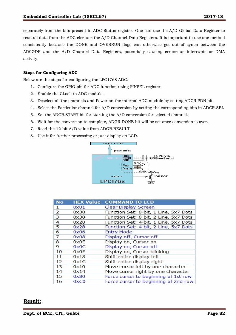
Embedded Controller Lab (15ECL67) 2017-18
Dept. of ECE, CIT, Gubbi Page 82
separately from the bits present in ADC Status register. One can use the A/D Global Data Register to
read all data from the ADC else use the A/D Channel Data Registers. It is important to use one method
consistently because the DONE and OVERRUN flags can otherwise get out of synch between the
AD0GDR and the A/D Channel Data Registers, potentially causing erroneous interrupts or DMA
activity.
Steps for Configuring ADC
Below are the steps for configuring the LPC1768 ADC.
1. Configure the GPIO pin for ADC function using PINSEL register.
2. Enable the CLock to ADC module.
3. Deselect all the channels and Power on the internal ADC module by setting ADCR.PDN bit.
4. Select the Particular channel for A/D conversion by setting the corresponding bits in ADCR.SEL
5. Set the ADCR.START bit for starting the A/D conversion for selected channel.
6. Wait for the conversion to complete, ADGR.DONE bit will be set once conversion is over.
7. Read the 12-bit A/D value from ADGR.RESULT.
8. Use it for further processing or just display on LCD.
Result:
Embedded Controller Lab (15ECL67) 2017-18
Dept. of ECE, CIT, Gubbi Page 83
VIVA QUESTIONS
1. Name the number of ports in ARM Cortex M3
2. Name the number of pins in ARM Cortex M3
3. How to configure the ports as input and output ports
4. Name the important peripherals in ARM Cortex M3
5. List the flags present in ARM Cortex M3
6. Name the software and version of software used for interfacing
7. What is PWM and how to configure it
8. What is the step angle of a stepper motor used in lab.
9. How to vary the speed and direction of a stepper motor.
10. What is baud rate and how to select the baud rate
11. Name the different baud rates available
12. What is serial data transfer. What type of data transfer is used in experiment.
13. What is SPI? Name the IC used for interfacing
14. What are the digital inputs required for turning on Common Anode and common
Cathode display
15. Explain the logic behind the generation of square and triangular waveform using
DAC
16. Name the different pins of LCD
17. What is the meaning of 16X2 in LCD
18. Name the number of scanning lines and return lines in the keypad
19. What is the difference between binary and BCD. Write the binary and BCD value
for 0xC9
20. Name the profile used in Cortex M3
Embedded Controller Lab (15ECL67) 2017-18
Dept. of ECE, CIT, Gubbi Page 84
QUESTION BANK
1. Display “Hello World” message using Internal UART.
2. Interface and Control a DC Motor.
3. Interface a Stepper motor and rotate it in anti-clockwise direction.
4. Interface a DAC and generate Square waveforms.
5. Interface a 4x4 keyboard and display the key code on an LCD.
6. Using the Internal PWM module of ARM controller generate PWM and vary its duty
cycle.
7. Demonstrate the use of an external interrupt to toggle an LED On/Off.
8. Display the Hex digits 0 to F on a 7-segment LED interface, with an appropriate
delay in between.
9. Interface a simple Switch and display its status through Relay, Buzzer and LED.
10. Measure ambient temperature using a sensor and SPI ADC IC.
11. Interface a Stepper motor and rotate it in clockwise direction.
12. Display the BCD digits 0 to 9 on a 7-segment LED interface, with an appropriate delay in between.
13. Interface a DAC and generate Triangular waveforms.