Introduction Class-D Efficiency - Intersil · PDF fileClass-D Audio II Evaluation Board...
17
Class-D Audio II Evaluation Board (HIP4080AEVAL2) USER’s MANUAL AN9525 Rev.2.00 Page 1 of 17 March 1996 AN9525 Rev.2.00 March 1996 Introduction Historically, audio amplifiers have been configured as Class A, B or A/B and the art of design is well-known. Also well known is the poor efficiency of these types compared to that of Class-D amplifiers. Motor drive and power supply designers have been using Class-D (switching) amplifiers for many years because use of linear amplifiers would incur excessive power loss, except when driving tiny loads. When evaluating Class-D amplifiers in the audio bandwidth, Intersil has made available the HIP4080AEVAL2 Evaluation Board as a tool that enables the audio designer to immediately evaluate the Class-D topol- ogy. This Application Note will refer to this evaluation platform periodically (See also datasheet File Number 4018). Whereas the theoretical best efficiency for Class-B amplifiers is 78%, the practical upper limit is more nearly 70% when driv- ing a purely resistive load. But when driving real speaker loads which can have power factor angles of 60 degrees or more, efficiency can deteriorate to 55% or less. Class-D amplifiers, however, can attain efficiencies of 90%, and with careful component choices can exceed 95% efficiency. More- over, the power factor of the load doesn’t affect the on-state power losses in the MOSFET switches normally used in these amplifiers. Using Class-D techniques, amplifiers capable of delivering several hundred watts to the load can be designed using small, inexpensive, stamped heat sinks. To review how poorly the efficiency of Class-B amplifiers can be, Figure 1 shows the ideal efficiency of a Class-B amplifier. The solid curve shows the ideal efficiency as a function of the power factor angle of the load current with respect to the applied load voltage. The dotted curve assumes that the peak output voltage will be 90% of the DC bus voltage level, which reflects a more realistic maximum efficiency level for various stray resistances in the output circuit. The efficiency plots in Figure 1 do not include any losses due to bias current of the Class-B amplifier, used to minimize crossover distortion, which occurs as one of the transistors in the totem pole turns off and the other turns on. The bias power loss is the product of the bias current and the total bus voltage impressed across the output transistors and will fur- ther degrade Class-B efficiency shown in Figure 1. Efficiency of Class-D amplifiers opens the possibility for powerful, small, light amplifiers with good sound quality to be designed today. The HIP4080A and related Intersil Intelligent Power Products ICs greatly simplify Class-D designs. Class-D Efficiency Class-D efficiency is largely determined by the ratio of the load resistance to the total DC loop resistance which is the sum of the r DS(ON) of the MOSFETs, wire resistances (including the output filter) and current sense resistor if used, and the load resistance. For highest efficiency, the MOSFET r DS(ON) resistances, shunt and filter resistances should be small compared to the load resistance. In audio Class-D applications, MOSFETs are used instead of IGBTs and Bipo- lar transistors because the switching frequencies required to keep distortion low at 20kHz signal frequencies can exceed 150kHz and neither Bipolar Power Transistors or IGBTs Switch efficiently at such high frequencies. FIGURE 1. IDEAL/REALISTIC CLASS-B EFFICIENCY For load current to flow in the Class-D bridge, two switches must be on simultaneously. The current flows through these, the stray and filter resistances, and the load. The instanta- neous load current is related to the bus voltage as follows, where R X includes all stray and filter resistances: The RMS load current is related to the peak value of the load current and hence the DC bus voltage, due to the sinusoidal nature of the load current, as follows: 80 75 70 65 60 55 50 45 40 0 10 20 30 40 50 60 70 80 90 POWER FACTOR ANGLE () k 2 = 0.9 (, k 1 ) (, k 2 ) k 1 = 1 V BUS = I LOAD 2 r DSON R X R + LOAD + (EQ. 1) I RMS V BUS 2 2 r DSON + R LOAD R X + --------------------------------------------------------------------------------------- = (EQ. 2)
Transcript of Introduction Class-D Efficiency - Intersil · PDF fileClass-D Audio II Evaluation Board...

Class-D Audio II Evaluation Board (HIP4080AEVAL2)
USER’s MANUAL
AN9525Rev.2.00
March 1996
IntroductionHistorically, audio amplifiers have been configured as Class A,B or A/B and the art of design is well-known. Also well known isthe poor efficiency of these types compared to that of Class-Damplifiers. Motor drive and power supply designers have beenusing Class-D (switching) amplifiers for many years becauseuse of linear amplifiers would incur excessive power loss,except when driving tiny loads. When evaluating Class-Damplifiers in the audio bandwidth, Intersil has made availablethe HIP4080AEVAL2 Evaluation Board as a tool that enablesthe audio designer to immediately evaluate the Class-D topol-ogy. This Application Note will refer to this evaluation platformperiodically (See also datasheet File Number 4018).
Whereas the theoretical best efficiency for Class-B amplifiersis 78%, the practical upper limit is more nearly 70% when driv-ing a purely resistive load. But when driving real speakerloads which can have power factor angles of 60 degrees ormore, efficiency can deteriorate to 55% or less. Class-Damplifiers, however, can attain efficiencies of 90%, and withcareful component choices can exceed 95% efficiency. More-over, the power factor of the load doesn’t affect the on-statepower losses in the MOSFET switches normally used in theseamplifiers. Using Class-D techniques, amplifiers capable ofdelivering several hundred watts to the load can be designedusing small, inexpensive, stamped heat sinks.
To review how poorly the efficiency of Class-B amplifiers canbe, Figure 1 shows the ideal efficiency of a Class-B amplifier.The solid curve shows the ideal efficiency as a function ofthe power factor angle of the load current with respect to theapplied load voltage. The dotted curve assumes that thepeak output voltage will be 90% of the DC bus voltage level,which reflects a more realistic maximum efficiency level forvarious stray resistances in the output circuit.
The efficiency plots in Figure 1 do not include any losses dueto bias current of the Class-B amplifier, used to minimizecrossover distortion, which occurs as one of the transistorsin the totem pole turns off and the other turns on. The biaspower loss is the product of the bias current and the total busvoltage impressed across the output transistors and will fur-ther degrade Class-B efficiency shown in Figure 1.
Efficiency of Class-D amplifiers opens the possibility forpowerful, small, light amplifiers with good sound quality to bedesigned today. The HIP4080A and related Intersil IntelligentPower Products ICs greatly simplify Class-D designs.
Class-D EfficiencyClass-D efficiency is largely determined by the ratio of theload resistance to the total DC loop resistance which is thesum of the rDS(ON) of the MOSFETs, wire resistances(including the output filter) and current sense resistor if used,and the load resistance. For highest efficiency, the MOSFETrDS(ON) resistances, shunt and filter resistances should besmall compared to the load resistance. In audio Class-Dapplications, MOSFETs are used instead of IGBTs and Bipo-lar transistors because the switching frequencies required tokeep distortion low at 20kHz signal frequencies can exceed150kHz and neither Bipolar Power Transistors or IGBTsSwitch efficiently at such high frequencies.
FIGURE 1. IDEAL/REALISTIC CLASS-B EFFICIENCY
For load current to flow in the Class-D bridge, two switchesmust be on simultaneously. The current flows through these,the stray and filter resistances, and the load. The instanta-neous load current is related to the bus voltage as follows,where RX includes all stray and filter resistances:
The RMS load current is related to the peak value of the loadcurrent and hence the DC bus voltage, due to the sinusoidalnature of the load current, as follows:
80
75
70
65
60
55
50
45
400 10 20 30 40 50 60 70 80 90
POWER FACTOR ANGLE ()
k2 = 0.9
(, k1)
(, k2)
k1 = 1
VBUS= ILOAD 2 rDSON RX R+ LOAD+ (EQ. 1)
IRMS
VBUS
2 2 rDSON + RLOAD RX+ ----------------------------------------------------------------------------------------= (EQ. 2)
AN9525 Rev.2.00 Page 1 of 17March 1996

Class-D Audio II Evaluation Board
(HIP4080AEVAL2)
The power delivered to the load is the product of the squareof the RMS load current and the load resistance, as Equa-tion 3 shows:
or, in terms of the bus voltage as Equation 4 shows:
The total power is the product of the square of the RMS loadcurrent and the sum of the load, filter, stray wiring andrDS(ON) resistances of the two series MOSFETs as shown inEquation 5. The resistance, RX, is the sum of all stray circuitresistances connecting the bridge with the load, includingthe resistances of the filter inductors, if any.
If switching losses could be ignored, Class-D efficiency issimply the ratio of the load resistance to the total power cir-cuit resistance as viewed from the Bus supply as shown inEquation 6.
With switching losses included, the total power dissipation andefficiency can be described as shown in Equation 7 and Equa-tion 8 respectively, which are fully developed in theAppendix.
For example, using the RFP22N10 MOSFET with a 4 load,a bus voltage of 36V, at a switching frequency of 240kHz, acommutation rate of 100A/s, and a reverse recovery time,tRR, of 100ns as shown below, would yield an operating effi-ciency of 84.1% given the conditions below.
If the tRR jumps to 200ns, the efficiency decreases to 72.5%,so the MOSFET body diode recovery time plays an import-ant role in determining efficiency.
Load impedance, also influences efficiency: For the valuesused above for the RFP22N10, the efficiency goes from84.1% to 84.8% with an 8 load when switching losses aretaken into account. With a 2 load, efficiency drops to 77.7%.
Nevertheless, Class-D efficiencies are much higher thancomparable Class-A and Class-AB Systems. To optimizeClass-D efficiency, one has to minimize the conduction andswitching losses.
Figure 2 shows measured efficiency at a DC bus voltage of30V using an Audio Precision Tester to calculate outputpower into a purely resistive 4 load. Notice that at very lowoutput power, that the efficiency drops off dramatically. Theonset of clipping of the output voltage waveform with a 30V.bus voltage occurred at an output power of 94W.
FIGURE 2. EFFICIENCY vs OUTPUT POWER (W)
MOSFET Choice, Bridge Dissipation
In order to properly choose the MOSFET switches (and heatsinks, if required by the design) one must be able to predictthe MOSFET conduction and switching losses at the maxi-mum power output of the amplifier. The full development, end-ing in Equation 9 below, is given in the Appendix. It is basedupon the value of total power dissipation less sum of the loadand stray power dissipation values previously calculated. Onefourth of the bridge dissipation is the power developed in asingle MOSFET switch.
In choosing MOSFETs, keep in mind that while a largerMOSFET goes hand-in-hand with minimizing the rDSON, thegate capacitance increases with MOSFET size. Also the tRRincreases with MOSFET size. These comments apply to
PLOAD = IRMS 2 RLOAD (EQ. 3)
PLOAD = 12---
VBUS2
2 rDSON RLOAD RX+ + 2----------------------------------------------------------------------------- RLOAD (EQ. 4)
PTOTAL =
12--- VBUS
2
2 rDSON RLOAD RX+ +-------------------------------------------------------------------- (EQ. 5)
RLOAD
2 rDSON RLOAD RX+ +--------------------------------------------------------------------= (EQ. 6)
PTOTAL
VBUS2
2---------------
2 rDSON RLOAD RX+ + -------------------------------------------------------------------------= . . .
+fPWM VBUS 2
VBUS2 rDSON RLOAD RX+ +--------------------------------------------------------------------
2---
IRATE-----------------------------------------------------------------------------------
2
. . .
+ IRATE tRR2
(EQ. 7)
(EQ. 8)
RLOAD2 rDSON RLOAD RX+ + -------------------------------------------------------------------------
1 fPWM
16 VBUS
2IRATE 2 rDSON RLOAD RX+ +
----------------------------------------------------------------------------------------------------------- . . .+
-------------------------------------------------------------------------------------------------------------------------------------------------------=
+ 2 IRATE
tRR2
VBUS--------------- 2 rDSON RLOAD RX+ +
RLOAD 4 = rDSON 0.08= VBUS 36 V=
IRATE 100AMPs
-------------= tRR 100 ns,= fPWM 240 kHz=
0 20 40 60 80 10030
40
50
60
70
80
90
OUTPUT POWER (W)
EF
FIC
IEN
CY
(%
)
(EQ. 9)PBRIDGE
VBUS2 rDSON RLOAD RX+ +-------------------------------------------------------------------- 2
rDSON= . . .
+ fPWM VBUS 2
VBUS2 rDSON RLOAD RX+ +-------------------------------------------------------------------
2---
IRATE----------------------------------------------------------------------------------
2
IRATE tRR2+
AN9525 Rev.2.00 Page 2 of 17March 1996

Class-D Audio II Evaluation Board
(HIP4080AEVAL2)
MOSFETs generally. Nevertheless there is no substitute forstudying the MOSFET Data Sheet. Even then, physical mea-surements are sometimes the only way to know for certainwhat commutation di/dt and reverse recovery time will resultin a given situation.
Since minimizing the sum of both switching and conductionlosses at the design frequency of interest will provide maxi-mum efficiency of Class-D switching amplifiers, an under-standing of the power dissipation components shown inEquation 9 which make up total MOSFET power dissipationis a must. See end-note [3] prior to the Appendix section.
Finally, the designer must weigh the cost tradeoff of heatsinking along with the cost of the MOSFETs in order to mini-mize the total system cost. The least expensive power sec-tion, moreover, may not be the most efficient.
Overcurrent and Short Circuit Protection
Audio amplifiers provide a voltage gain to amplify a signalfrom a preamplifier output. If the output is shorted, the ampli-fier will try to provide sufficient current to establish a voltageat the output which is equal to the input signal multiplied bythe gain of the amplifier. Short circuit protection will helpreduce down time and expensive repairs.
In addition to short-circuit protection, some form of currentlimit protection will reduce the output voltage applied acrossthe load and can help to protect the amplifier and its loadfrom overheating. The amplifier can also be protected fromthose who would connect too many speakers across the out-put or connect a speaker with too low an impedance.
Both of these fault modes, the direct short and the overload,require different protection schemes. In the case of the directshort, one usually wishes to disable the output drive as rap-idly as possible and call attention to the condition by requir-ing some direct intervention by an operator to “reset” theamplifier. This can be as simple as incorporation of a resetbutton on the back of the amplifier, or a bit more inconve-niently by requiring amplifier power down.
In the Intersil HIP4080AEVAL2 Audio Amplifier Board (referto schematic at end of this application note), a reset buttonon the PC Board resets the amplifier after an overcurrent isdetected. This level can be set via potentiometer, P4, fromapproximately 0A to 80A. (Tolerance, approximately 10%.)
The current limit circuit is of the spillover type, which meansthat when the current limit level is reached, the output of opamp, U5D, swings toward the +12V rail from its normal zerovolt level. When the current reaches a level which turns onJFET, Q1, current is pulled through R14 at the output of theerror amplifier, U5A. The op amps used in the HIP4080Ademo board are Intersil type CA5470. The magnitude of thevoltage output of the error amplifier is reduced before beingcompared with the triangle wave signal at the HIP4080A IN+input pin. The current limit level, set by P2, provides overcur-rent settings from approximately 0A to 80A. with a tolerance ofapproximately 10%.
The HIP4080A’s internal comparator compares the trianglewave and the error signal from the error amplifier, creating aPulse Width Modulation signal, PWM. The PWM signal con-
trols the gate outputs of the HIP4080A, which in turn controlthe power MOSFETs. The output of the MOSFET bridge isessentially a high voltage representation of the PWM wave-form at the comparator output. When filtered by the low passfilter and the speaker load, this power PWM signal recon-structs the original audio input signal.
The short-circuit and current limit protection derive their cur-rent feedback signals from a 0.1 dropping resistor in theMOSFET bridge. Comparator U1B compares this feedbacksignal with the voltage set up by voltage divider, R4 in serieswith P4. The comparator output, normally at ground poten-tial, will swing high under short circuit conditions and togglethe RESET pin of the U2A (D-Latch), in turn pulling the DIS(disable) pin of the HIP4080A high, disabling all gate outputsof the driver IC and turning off all MOSFETs in the bridge.The comparators used in the HIP4080A demo board areIntersil type CA3290.
During power up of the 12V supply to the HIP4080AEVAL2Board, the U2A D-latch, Intersil type CA4013, is also reset,thereby, disabling the HIP4080A driver until after a timedelay set-up by resistor, R7, and capacitor, C7. When theexponentially increasing voltage on C7 reaches or exceeds6V, the output of comparator, U1A provides a positive clockpulse to the D-latch, thereby setting it. This action causesthe LED, D1, to extinguish and the DIS pin of the HIP4080Ato be pulled low, releasing gate pulses to the MOSFETbridge and enabling the amplifier output.
The HIP4080AEVAL2 demo doesn’t include a reliablemeans to short the error amplifier feedback circuit duringpower-up. As a result, “thumping” might be encounteredduring power-up. New designs should attempt to avoid this.
Power Supply/Biasing Considerations
Simplicity and low cost were also goals of the HIP4080AE-VAL2 design. Consequently a single-polarity 12V power sup-ply was chosen. Twelve volts avoids overdriving the MOSFETgates which would increase the internal power dissipation ofthe HIP4080A. Using 12V rather than +15V also decreasesturn-off times of the power MOSFETs, thereby reducing some-what the Miller feedback effect as well as the commutationdi/dt rate and peak recovery current of the MOSFET bodydiodes due to a somewhat longer turn-on time.
Closing the Loop
Often, feedback techniques are used to linearize and main-tain tight, consistent control of amplifier gain and frequencyresponse. A high gain feedback loop will enhance transientresponse and minimize distortion over a wide frequencyrange. The frequency range of concern is 20Hz to 20kHz.
The design of the feedback loop to be used with a Class-Damplifier is a bit different from the one which might be used witha linear amplifier because there are no digital delays involved inthe linear amplifier. The basic feedback block diagram used willnevertheless take the form of that shown in Figure 3.
In order to maintain feedback loop stability where a switchingregulator or some other “digital” delay is involved, the feed-back loop must have a unity gain crossover frequency
AN9525 Rev.2.00 Page 3 of 17March 1996

Class-D Audio II Evaluation Board
(HIP4080AEVAL2)
(rad/sec.) less than or equal to half of the frequency repre-sented by the digital delay. In the Class-D amplifier there is adigital delay comprised of the PWM switching frequency. Soif the switching frequency is chosen to be roughly ten timesthe maximum desired output frequency, say 240kHz, thenunity gain crossover must be no higher than 120kHz.
FIGURE 3.
In analyzing the feedback loop, we don’t need to considerthe high-pass filter at the front end of the amplifier, whosemain purpose is to block DC input signals (or offsets) frombeing applied to the load. For simplicity purposes, we willalso ignore the current limit circuit, since it is a spillover typeand is not in the loop until the onset of current limiting. Theloop will be designed to maintain a phase margin of at least30 degrees.
With the above in mind, the control loop is comprised of theforward path which includes the error amplifier (IntersilCA5470), U5A, the pulse width modulator, PWM, comprisingthe triwave generator comparison with the error signal outputfrom the error amplifier, and the gain associated with theMOSFET bridge. The PWM-Bridge combination can be mod-eled as a fixed gain with a single order delay term equal to:
The feedback path of the feedback loop is comprised of thedifferential feedback amplifier, U5C, and the resistor whichfeeds the differential amplifier output signal to the error ampli-fier, U5A, summing junction. The differential amplifier gainshould be set equal to the reciprocal of the desired closed-loopgain. If a 20VRMS output is desired for a 1.0VRMS input signal,for example, then the differential amplifier gain should be 1/20.
The differential feedback amplifier should also have a slew rateof at least 5V/s unless input filtering is going to be used. If thisisn’t done, the feedback amplifier will not be able to respond tothe high signal slew rates at the output of the MOSFET bridgeinverter. The full power bandwidth capability should be at least0.5MHz, to minimize input filtering. The Intersil, Type CA5470op amp meets the minimum requirement with some input filter-ing so as not to exceed the amplifier’s slew rate and bandwidthcapabilities. The filter delays introduced into the feedback cir-cuit must be compensated for by a similar lead term (zero) inthe error amplifier transfer function. Since the feedback ampli-fier is a differential amplifier, the impedances looking out ofeach summing junction must be matched to ensure good com-mon-mode rejection, since the common-mode voltage will con-tain large components of the switching frequency.
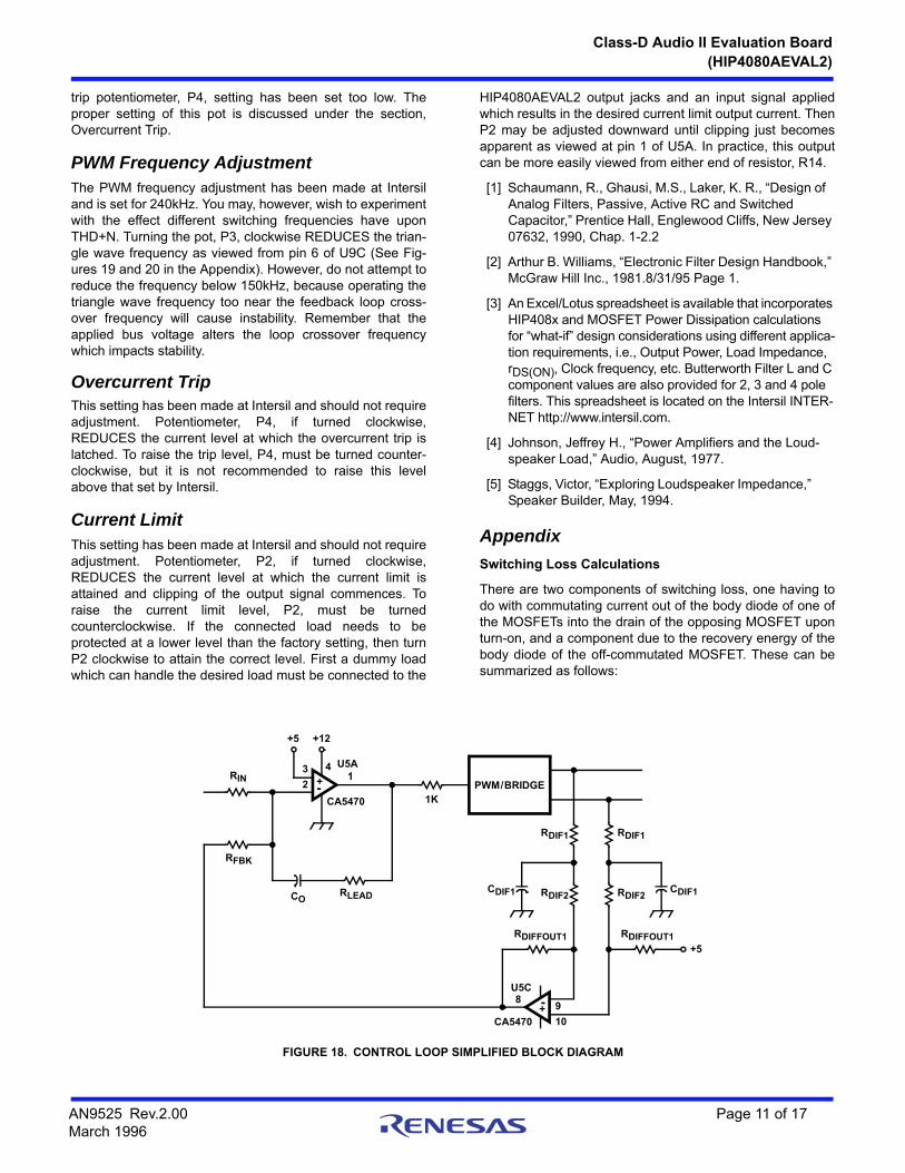
A simplified combination schematic/block diagram is shown inFigure 18 and a full schematic of the HIP4080AEVAL2 printedcircuit board is shown in Figures 19 and 20 in the Appendix.
The generalized feedback control system is modeled basicallyas a forward gain block, G, whose input is the error signal fromthe loop summing node, and whose output is the output to thespeaker. See Figure 3. “C” represents the input control signaland “R” represents the response or output. The summingnode for the audio system is the inverting summing junctionof the error amplifier, U5A, which actually sums currents.The equation which describes its transfer function can beeasily developed, since we know that the gain of an invertingoperational amplifier is simply the feedback impedancedivided by the input impedance. Therefore, the error ampli-fier transfer function is, where s is the Laplace operator:
The summing junction shown in Figure 4 sums currentsrather than voltages and the error amplifier sums the currentdifference between the RIN and the RFBK resistors such thatthe difference between the currents must flow in the feed-back impedance of the error amplifier.
FIGURE 4.
Block diagram transformation techniques can be used tosimplify Figure 4 so that the block representing the recipro-cal of RIN can be brought inside the loop, so that the controlloop will sum voltages again and look more like the blockdiagram of Figure 3. To do this, the control loop equationsrepresenting the open-loop gain and the forward gain mustbe identical before and after the transformation. So inFigure 4 if we bring the factor 1/RIN inside the loop, then theloop gain will have been reduced by the factor, RIN. So, theloop gain must be multiplied by the factor RIN to compensatefor the initial reduction. Figure 5 shows the transformed, butidentical section of the loop.
Notice that both the feed-forward and the loop gains of thesystems in Figure 4 and 5 are identical. The partial loopsshown in Figures 4 and 5 are incomplete because they don’tinclude the gain of the PWM-Bridge Inverter in the forwardpath and the gain of the differential amplifier in the feedbackpath.
The PWM-Bridge Inverter gain, heretofore referred to as KC,will be equal to simply twice the DC bus voltage divided bythe peak-to-peak triangle wave voltage. For the HIP4080AE-VAL2 demo, the bus voltage is approximately 36V and thepeak-to-peak triangle wave voltage is about 5.5V to 6V. SoKC is about 12. Keep in mind that there is a transport delaydue to the PWM switching frequency, which we could modelas a first order delay of the reciprocal of the PWM frequency.
GC R
H
+
-
12 fPWM---------------------------------
GERR
RLEAD CO s 1+
CO s----------------------------------------------------
RIN----------------------------------------------------=
(EQ. 10)
1RIN-----------
RLEAD CO s 1
CO s----------------------------------------------------------
1RFB-------------
C+
-
AN9525 Rev.2.00 Page 4 of 17March 1996

Class-D Audio II Evaluation Board
(HIP4080AEVAL2)
But if we just remember that we want to have unity open loopgain at about half of this frequency, we can ignore this delayin our analysis.
FIGURE 5.
The differential amplifier feedback gain, GDIF, is shown inEquation 11A. The gain of a differential amplifier is simplythe feedback impedance divided by the input impedancelooking into the inverting input, provided that the impedanceslooking out of both summing junctions are exactly equal.That is why we specified earlier that tightly matched resistorsshould be used for the resistances making up this circuit.Usually 1% resistors are good enough, but the final decisionis determined by how much common-mode rejection isdesired. The quantification of the common-mode gain withcomponent tolerance is outside the scope of this applicationnote, but any good book on operational amplifier design andapplications will go into this subject in detail.
where:
FIGURE 6. COMPLETED CLOSED-LOOP
The completed closed-loop Audio System Block Diagram isshown in Figure 6.
Figure 6 shows a forward gain block and a feedback gainblock. Control theory requires that for closed loop stability,the open loop gain must be less than unity when the phaseshift equals or exceeds 180 degrees. Also for frequenciesbelow unity gain crossover, the closed loop gain (what theamplifier actually looks like if it were in a black box), 1/H, isthe reciprocal of the feedback gain block. At frequenciesabove the crossover frequency, the closed loop gainapproaches the magnitude of the forward gain block (i.e.,what you would have if there were no feedback at all). Thereis little practical interest in frequencies above unity gaincrossover, because the feedback effect is minimal there.
A closer look at Figure 6 shows that there is a zero in the for-ward gain block and a pole in the feedback gain block. If thetime constants associated with the pole and zero are exactlyequal, then their effect on the loop gain is eliminated and theloop looks like a pure integrator and is a Type 1 system withrespect to output voltage, the variable being measured bythe feedback. This type of loop exhibits zero error at DC,with increasing following errors at higher frequencies aspredicated by the open loop gain at those frequencies.
What effect will certain changes in several component val-ues have on performance? Decreasing RIN will increase themagnitude of the output voltage of the audio amplifier with-out changing the open loop gain (stability and response areunaffected). This is because RIN is in the denominator termof the forward gain and in the numerator of the feedbackblock. Increasing the feedback resistor, RFBK, will increasethe closed loop gain, but it will decrease open-loop gain andwill therefore, have an effect on stability and response, sothis component should never be used only to adjust ampli-tude gain of the amplifier.
If the feedback gain of the loop is satisfactory (you get thedesired output amplitude for a given input signal magnitude),you can increase the open loop gain without disturbing thefeedback gain by decreasing the value of CO. To decreasethe open loop gain, you can increase the capacitance valueof CO. Variations in bus voltage directly affect the gain con-stant, KC, and the open-loop gain as well. Therefore, theopen loop gain must provide stability at the highest bus volt-age operating level which will be encountered. Ideally, thebus voltage won’t vary a lot and this won’t be a major con-cern. It could be a concern when attempting an amplifierdesign which is intended to be used on a variety of DC busvoltage levels. One way to avoid a problem is to increaseRFBK in proportion to any increase in bus voltage. While thiswill increase the closed loop gain, this is probably desirableso that the maximum output can be obtained from a constantinput level, while keeping open loop gain constant.
The Bode plots shown in Figure 7 show a nice linear roll off withfrequency of the open loop gain with a unity gain crossover ofapproximately 150kHz. The phase margin which is the angulardifference between 180 degrees and the phase lag of the openloop gain (150 degrees for the compensation shown inFigure 7) is 30 degrees and the loop will be stable andreasonably damped. Further increases in open-loop gain will ofcourse raise the crossover frequency of the loop and willencourage instability due to the switching frequency of thePWM. Crossover frequency increases must be accompaniedby proportional increases in switching frequency. Unfortunately,this also tends to reduce efficiency due to increases in recoverylosses and commutation losses in the bridge inverter.
Output Filter Requirements and DesignClass-D amplifiers differ from linear amplifiers in that switch-ing amplifiers require an output filter capable of removing thehigh frequency components of the PWM waveform. Theswitching frequency components, while not audible, will radi-ate EMI from the wires going to the speaker. In cases wherethe speaker will be located together with the amplifier (pow-
RLEAD CO s 1+
RIN CO s---------------------------------------------------------
RINRFBK-----------------
C+
-
GDIF
RDIFFOUTRDIF1 RDIF2+----------------------------------------
1 DIF s+----------------------------------------= (EQ. 11A)
DIF
RDIF1 RDIF2
RDIF1 RDIF2+----------------------------------------- CDI= (EQ. 11B)
1 LEAD s+
RIN CO s--------------------------------------- KC
RINRFBK-----------------
RDIFFOUTRDIF1 RDIF2+--------------------------------------------
1 DIF s+--------------------------------------------
C R+
-
AN9525 Rev.2.00 Page 5 of 17March 1996

Class-D Audio II Evaluation Board
(HIP4080AEVAL2)
ered speakers), the filtering may be either simplified or elimi-nated by appropriate shielding techniques. Several types offilter designs can be used and their advantages, disadvan-tages and design go beyond the scope of this applicationnote. Several good references are available which will behelpful in the evaluation and synthesis of the popular filtertypes available (see end-notes [1] and [2]).
FIGURE 7.
The Butterworth Filter has a frequency response character-istic which most nearly fits the asymptotic response of a lowpass filter of n-th order. The 4 pole Butterworth Filter rolls offat 80dB per decade of frequency. The Chebyshev Filterexhibits slightly sharper attenuation with frequency than theButterworth, but with somewhat higher phase shift or signaldelay. The Bessel Filter is optimized to produce a maximallyflat delay in the passband and the step response has virtu-ally no overshoot or ringing and the impulse responsedoesn’t oscillate, but the frequency response is much lessselective than in the other types and roll-off is not nearly assharp as with the other types.
The HIP4080AEVAL2 Demo Board was designed using a4-pole Butterworth Filter. Table 12-2 in the Electronic FilterDesign Handbook was used to derive the values for a 4load. A cut-off frequency of 30kHz was chosen and it wasassumed that the source resistance of the inverter bridgewas 0.1. The values derived for the two inductors were32.5H and 23H, respectively, and for the capacitors,2.1F and 0.508F, respectively.
The sample calculation for the normalized filter componentvalues shown in Equation 12 are based upon 30kHz and 4,respectively, for the cutoff frequency and load impedance.Equations 13 and 14 show the equations which transformthe normalized values into the actual values required for thefilter. The cutoff frequency in radians/sec. are calculatedfrom the desired cutoff frequency in Hz using Equation 15.
The Electronic Filter Design Handbook [2], Table 12-2 showstables for normalized values for these filters. For the 4-polefilter, assuming 0.1 source impedance at the bridge inputend of the filter, the normalized values are:
FIGURE 8.
The normalized values (see Figure 8) must be transformedto actual inductance and capacitance values at the cutoff fre-quency and load impedance desired using the following nor-malization transformations,
for the inductors:
and for the capacitors:
where 3dB is the cutoff frequency in radians per secondand RN is the desired load resistance in ohms.
Therefore;
and; RN = 4 for the HIP4080AEVAL2 Board. When thetransformations shown above are performed, the followingactual values for the filter components result:
Notice from the filter component transformation equationsabove that the actual values of the filter components aredependent upon the normalizing load resistance and the cut-off frequency. Both inductances and capacitances varyinversely with frequency, whereas inductances vary directlywith load resistance and capacitances vary inversely withload resistance. For example, if the load resistance waschanged to 8 then the capacitor values calculated abovewould be halved and the inductor values doubled if the cutofffrequency remained 30kHz.
Since the HIP4080AEVAL2 filter employs 2 inductors in eachof the two output lines and 4 capacitors instead of two, thevalues of the inductors must be halved and the capacitorsdoubled as shown in Figure 9.
FIGURE 9. HIP4080AEVAL2 FILTER IMPLEMENTATION
100 1000 1•105-180
-160
-140
-120
-100
-80
-60
-40
-20
0
20
40
60
80
FREQUENCY (Hz)
GA
IN (
dB
) A
ND
PH
AS
E (
DE
GR
EE
S)
1•1061•104
DIF1–
2 -----------
LEAD1–
2 ------------------
20 GHK log
GHK arg180
----------
L1N : 1.5307= L3N : 1.0824=
C2N : 1.5772= C4N : 0.3827= (EQ. 12)
C4NC2N RLOAD = RN
L3NL1N
SOURCE
LI LINRN3dB--------------= L3 L3N
RN3dB--------------= (EQ. 13)
C2C2N
RN 3dB----------------------------= C4
C4NRN 3dB----------------------------= (EQ. 14)
3dB: 2 30 kHz= 3dB: 1.885 105 RAD
SEC-------------= (EQ. 15)
L1 32.482 H=L3 22.969 H=C2 2.092 F=C4 0.508 F=
L3/2L1/2
TO
2 x C42 x C2
RLOAD
L3/2L1/2
2 x C42 x C2
BRIDGE
AN9525 Rev.2.00 Page 6 of 17March 1996

Class-D Audio II Evaluation Board
(HIP4080AEVAL2)
Zobel Filter
In addition to the filter used to remove the PWM switchingfrequency content from speaker leads which may be routednear sensitive electronics, a Zobel Filter is used to make thechosen speaker look like a pure resistive load. With linearamplifiers, any phase delay between voltage and current inthe output waveform would naturally result in a reducedpower factor and a corresponding reduction in efficiency. Ofcourse the efficiency of these amplifiers was already pooreven at unity load power factor.
The normalized filter design tables assume that the load ispurely resistive. Deviations from a pure resistive load causesfilter pole shifting and deviation from the filter’s characteristicperformance.
Fortunately, it is easy to design a Zobel Filter, which basi-cally consists of a series R-C circuit which is placed directlyin parallel with the speaker load, which is assumed to be pre-dominately a series R-L circuit. By setting the Zobel Capaci-tor equal to the inductance of the load divided by the squareof the load resistance, cancellation of the load filter combina-tion’s reactance is facilitated and the combination looks justlike the load resistance, R.
The Zobel Network Resistor in series with CZOBEL is setequal to the resistance of the load or speaker voice coilresistance. More information about compensating speakersis found in end-notes [4] and [5].
Conclusions
Distortion
Audiofiles and designers of audio amplifiers worry thatClass-D amplifiers will exhibit excessive harmonic distortion.While the distortion plus noise at the highest frequenciesseems to be somewhat higher than exhibited by linear ampli-fiers, the THD of Class-D amplifiers can be kept down to 1%or lower at the high end of the frequency range.
At the low end of the frequency range, Class-D amplifiersexhibit lower THD than Class-AB amplifiers exhibit.Crossover distortion of the Class-AB amplifier appears tocause this low-end distortion. Class-D exhibits distortionrelated to switching transients in the inverter bridge, which isgenerally low.
Nevertheless, at the high end of the frequency spectrum,Class-D amplifiers exhibit increasing THD, perhaps reachingor exceeding 1% at 20kHz and above. This phenomenonseems to be a result of open loop gain roll-off as the feed-back loop crossover frequency is approached. The feedbackloop exhibits less and less ability to adjust for distortion in theoutput waveforms as this point is reached. The gain of theHIP4080AEVAL2 Demo is about 10 at 20kHz, which meansthat the output signals will duplicate the input command sig-nal with a following error of 10%. Fortunately, this doesn’tmean that the resulting THD will be 10%, but it can contrib-ute to an increase in distortion with frequency.
Another contributor to distortion is ringing on the PWMoutput terminals of the amplifier. Trapped inductancesbetween the MOSFETs in an inverter leg of the bridge causetransient voltages comprising very high frequencycomponents. Also, small discontinuities in the outputwaveform caused by the amount of dead time betweenupper and lower MOSFET conduction periods adds todistortion. While these components are beyond the cutofffrequency of the filter, some of these components make itthrough the filter and add to distortion. Figure 10 showsactual THD + N% versus frequency for the HIP4080AEVAL2Demo Board which used a function generator to produce amore linear triangle wave than is produced by the on-boardtriangle wave generator. Distortion was found to be cut byhalf to two-thirds through use of an off-board linear trianglewave generator.
FIGURE 10.
In Figure 10, using 3kHz as a reference point, the plots fromtop to bottom reflect the THD + N% at output power of 70W,25W, 5W and 1W respectively. The Audio Precision internalfilters were set at 22Hz and 30kHz for the low and high fre-quency filters, respectively.
The trend toward higher distortion with rising frequencywould occur even without a feedback loop, since the fixedPWM switching frequency and dead-time content meansthat at high frequencies the dead-time content occurs overa larger percentage of the output waveform cycle thanthey do at low frequencies. Also, an uneven distribution ofthese components undoubtedly occur from half-cycle tohalf-cycle.
Proof of the fact that the switching frequency effects the levelof THD + N% can be seen from Figure 11, which showsTHD + N% as PWM frequency is varied from 150kHz to350kHz. The lowest distortion results occur at a switchingfrequency of 150kHz and the highest occurs at a switchingfrequency of 350kHz. At 100kHz, however, the distortiongrows very large as the loop becomes unstable and thedistortion is clearly evident in the output waveform. Thecurves in Figure 11 were created at a constant output powerof 5W and a DC bus voltage of 30V using the AudioPrecision 30kHz internal low-pass filter.
CZOBEL
LLOAD
RLOAD2
--------------------= (EQ. 16)
5
0.01020 10K 20K
28 JUL 95 15:19:11
TH
D +
N (
%)
FREQUENCY (Hz)
100 1K
0.1
Ap
1
AN9525 Rev.2.00 Page 7 of 17March 1996

Class-D Audio II Evaluation Board
(HIP4080AEVAL2)
FIGURE 11. THD + N (%) vs FREQUENCY (Hz)
One other improvement was made which is reflected in gen-erally lower distortion figures in Figure 12. The addition ofphase to ground series R-C snubbers substantially reducethe voltage transients as viewed from the output terminals ofthe MOSFET bridge as power is swept from 0.3W to 100Wat 1kHz. The snubbers reduce the THD + N% and protect theMOSFETs and the HIP4080A from undue voltage stress andpossible failure. More about this in the “Other Design Con-siderations” Section.
FIGURE 12. THD +N (%) vs OUTPUT POWER
Figure 13 shows a sweep of THD + N% as a function of inputamplitude in VRMS at two different excitation frequencies.The lowest value produced 1W into a 4 load, while thelargest input value of 1V corresponded to 100W into the 4load. The lower curve represents an input frequency of 1kHzand the upper represents an input frequency of 10kHz. Asexpected, the higher frequency produces more distortion asit becomes increasingly difficult for the control loop toregulate and as the dead-time content becomes a larger partof each cycle of the output waveform as mentioned earlier.The PWM switching frequency for this test was 240kHz,although as Figure 11 shows, better results might have beenattained had 150kHz been used. In conclusion, listeningtests indicate that the measured distortion of around 1% in
the neighborhood of 20kHz is not discernible to the humanear, whereas distortion at the lower end of the frequencyspectrum can be noticeable. But this is the very area wherethe Class-D amplifier shines.
FIGURE 13. THD + N (%) vs AMPLITUDE (VRMS)
Intermodulation Distortion
Figure 14 shows CCIF % intermodulation distortion as afunction of input amplitude with a 30V bus voltage.Approximately 100W is output with the input at 2.0VRMS.The intermodulation distortion is comparable with the betterClass B amplifiers. The CCIF Test uses two equal amplitudehigh frequency stimulus signals closely spaced in frequency.For the HIP4080AEVAL2 testing 19kHz and 20kHz signalswere used. At the upper end of the power range, onset ofclipping occurred.Bandwidth
FIGURE 14.
Figure 15 shows the closed-loop frequency response of theHIP4080AEVAL2. The response is flat (under 0.5dB) from10Hz through 20kHz. The slight wiggle at the upper end ofthe passband may be due to the tolerance of the compo-nents within the 4-pole Butterworth Filter.
1
0.120 10K
01 SEP 95 05:59:38
FREQUENCY (Hz)100 1K
Ap
TH
D +
N (
%)
2
0.0500.3 100
05 OCT 95 00:04:19
TH
D +
N (
%)
OUTPUT POWER (W)
1 10
0.1
1
Ap
5
0.0500.1 1
28 JUL 95 15:02:22
AMPLITUDE (VRMS)
Ap
TH
D +
N (
%) 1
0.1INPUT FREQUENCY = 1kHz
INPUT FREQUENCY = 10kHz
2
1
0.1
0.0500.1 1 2
15 OCT 95 08:46:35
CC
IF IN
TE
RM
OD
UL
AT
ION
DIS
TO
RT
ION
(%
)
INPUT AMPLITUDE (VRMS)
Ap
AN9525 Rev.2.00 Page 8 of 17March 1996
Class-D Audio II Evaluation Board
(HIP4080AEVAL2)
FIGURE 15. CLOSED LOOP FREQUENCY RESPONSE
Signal to Noise Ratio
Figure 16 shows the signal-to-noise ratio of the HIP4080AE-VAL2 demo board, modified with the 2k resistor in series withthe input blocking capacitor. The two curves shown were per-formed with 1W and 10W output power to a 4 load. Excellentrejection seems possible with Class-D amplifiers.
FIGURE 16. SIGNAL-NOISE RATIO BANDPASS (dBr) vsBPBR (Hz)
Other Design Considerations
Transient Suppression
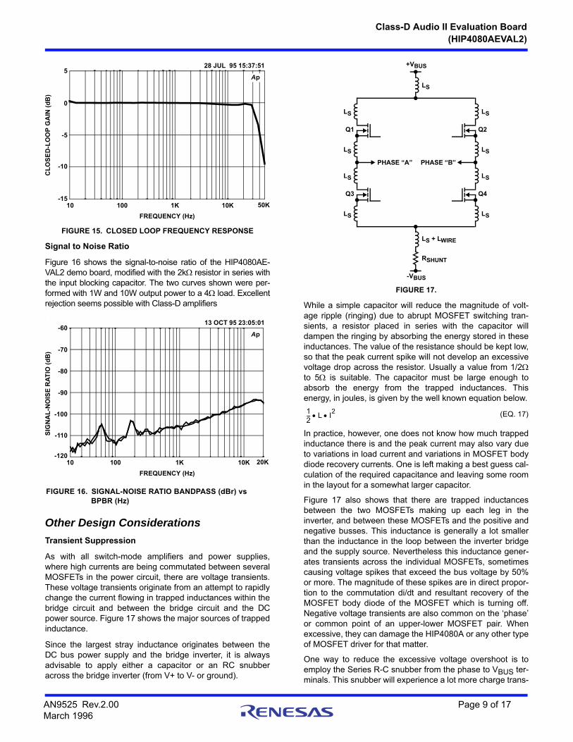
As with all switch-mode amplifiers and power supplies,where high currents are being commutated between severalMOSFETs in the power circuit, there are voltage transients.These voltage transients originate from an attempt to rapidlychange the current flowing in trapped inductances within thebridge circuit and between the bridge circuit and the DCpower source. Figure 17 shows the major sources of trappedinductance.
Since the largest stray inductance originates between theDC bus power supply and the bridge inverter, it is alwaysadvisable to apply either a capacitor or an RC snubberacross the bridge inverter (from V+ to V- or ground).
FIGURE 17.
While a simple capacitor will reduce the magnitude of volt-age ripple (ringing) due to abrupt MOSFET switching tran-sients, a resistor placed in series with the capacitor willdampen the ringing by absorbing the energy stored in theseinductances. The value of the resistance should be kept low,so that the peak current spike will not develop an excessivevoltage drop across the resistor. Usually a value from 1/2to 5 is suitable. The capacitor must be large enough toabsorb the energy from the trapped inductances. Thisenergy, in joules, is given by the well known equation below.
In practice, however, one does not know how much trappedinductance there is and the peak current may also vary dueto variations in load current and variations in MOSFET bodydiode recovery currents. One is left making a best guess cal-culation of the required capacitance and leaving some roomin the layout for a somewhat larger capacitor.
Figure 17 also shows that there are trapped inductancesbetween the two MOSFETs making up each leg in theinverter, and between these MOSFETs and the positive andnegative busses. This inductance is generally a lot smallerthan the inductance in the loop between the inverter bridgeand the supply source. Nevertheless this inductance gener-ates transients across the individual MOSFETs, sometimescausing voltage spikes that exceed the bus voltage by 50%or more. The magnitude of these spikes are in direct propor-tion to the commutation di/dt and resultant recovery of theMOSFET body diode of the MOSFET which is turning off.Negative voltage transients are also common on the ‘phase’or common point of an upper-lower MOSFET pair. Whenexcessive, they can damage the HIP4080A or any other typeof MOSFET driver for that matter.
One way to reduce the excessive voltage overshoot is toemploy the Series R-C snubber from the phase to VBUS ter-minals. This snubber will experience a lot more charge trans-
5
-1510 10K 50K
28 JUL 95 15:37:51
CL
OS
ED
-LO
OP
GA
IN (
dB
)
FREQUENCY (Hz)
100 1K
-5
0
-10
Ap
-60
-12010 10K 20K
13 OCT 95 23:05:01
SIG
NA
L-N
OIS
E R
AT
IO (
dB
)
FREQUENCY (Hz)
100 1K
-80
-70
-100
Ap
-90
-110
+VBUS
LS
LS
LS
Q2
PHASE “B”
LS
LS
Q4
PHASE “A”
-VBUS
LS + LWIRE
RSHUNT
LS
LS
Q1
LS
LS
Q3
12--- L I
2 (EQ. 17)
AN9525 Rev.2.00 Page 9 of 17March 1996

Class-D Audio II Evaluation Board
(HIP4080AEVAL2)
fer through it than does the DC bus snubber, because thephase voltage is a PWM-ed square wave operating at aswitching frequency, fPWM. The resulting power dissipation(watts) due to charging and discharging the snubber capaci-tor will be:
Almost all of this power will of necessity be expended in theseries snubber resistor. Judicious choice of capacitor valuewill result in using the smallest possible value of capacitancecapable of controlling the transients on the phase node toacceptably safe levels and will result in a resistor power rat-ing which is not so large as to cause your colleagues tosmirk. Another consideration is, of course, distortion, sinceexcessive phase voltage transients will translate into higherTHD+N levels.
Layout Requirements
The layout recommendation in this section will cover both rec-ommendations which we followed in laying out theHIP4080AEVAL2 Board and those which we subsequentlydiscovered would yield further improvements in performance.This is done so that designers can reap the greatest benefitsfrom Class-D amplifiers without having to reinvent the wheel.
The size of the snubber components mentioned previouslywill obviously be affected by the amount of trapped or strayinductances within the MOSFET inverter section. Therefore,techniques to minimize these inductances are worth theeffort. The trace distances between MOSFETs should beminimized. Also the trace lengths between the MOSFETsand the positive and negative DC busses should be short.Large loops in the inverter bridge circuit should be avoided.Strive to use ground planes for one or both bus polarities.For example, make the negative DC bus bottom side copperand the positive DC bus top side copper.
Usually several R-C snubbers placed between positive andnegative DC busses, one across each upper-lower MOSFETpair will minimize voltage transients and protect theMOSFETs and the driver IC. If some power supply ripple isexpected, much larger (i.e., electrolytic) capacitors must beused in addition to the R-C snubbers.
Consider a separate ground plane for the signal level ICcommon connections. To minimize transients from theinverter from impinging upon the HIP4080A connection ofthe ALS and BLS pins are best connected to the signal com-mon ground plane.
Component Choice
A good audio amplifier will require operational amplifiers withhigh gain-bandwidth product. The CA5470 amplifier used inthe HIP4080AEVAL2 is capable of use in systems with acrossover frequencies upwards of 150kHz. For higher cross-over frequencies choose a better amplifier. The amplifierused for the differential feedback should also have reason-ably low input offset voltage or offset nulling capability shouldbe added. The offset voltage of the amplifier reflected at theload will be 10 to 30 times greater depending upon theclosed-loop gain.
The CA5470 amplifier’s 15mV maximum offset can be almost0.5V at the load. High frequency operational amplifiers needeven more care in layout than low frequency op amps toensure that they don’t pick up noise from the power supplyand that stray signals don’t feed into the summing junctions.Therefore, keep the summing junction traces short and keepbias voltage traces away from high frequency signals. If indoubt place bypass capacitors on the power supply pins atsensitive op amps to enhance power supply rejection.
In performance evaluations of the HIP4080AEVAL2 Board, itwas noticed that the distortion dropped significantly whenthe input gain pot was not full maximum setting. This wasquickly traced to the fact that noise coming into the amplifierfrom external cables was coupled directly through the block-ing capacitor to the summing junction of U5B. The simpleaddition of a 2k resistor cured this problem and is a worth-while addition on new designs.
Setup ProceduresHookup
The HIP4080AEVAL2 Demo Board requires an external DCsource of power to operate the MOSFET bridge, and a sepa-rate low voltage DC power source to power the 12V DC reg-ulator which supplies power to the control ICs, bias circuitsand the HIP4080A.
The low voltage supply is connected to terminals J4 (positive15V to 20V) and J5 (negative or common). The high voltageDC (up to 40V maximum) should be connected to J2 (posi-tive) and J3 (negative or common). If the desired high volt-age DC supply is in the 15V to 20V region, one connectionmay be made for high and low DC power by bringing thehigh voltage into jacks J2 and J3 as described above and“jumpering” JP1 located between jacks J2 and J4 on theHIP4080AEVAL2 Demo Board. Since the on-board voltageregulator, U3 is a linear regulator, it will drop several voltsbetween its input (J4 to J5) and the regulated output valuewhich should be nominally 12VDC. For this reason, no lessthan 14V to 15V should be applied between J4 and J5.
The fuse, F1, is a 10A, 125V Buss GMC fuse which func-tions as backup protection for the Overcurrent Trip featurediscussed below.
The HIP4080AEVAL2 Demo Board is designed to operatebest with 4 loads, since the Zobel Filter design is designedfor a 4 load and a typical speaker coil inductance of 16H.The precise character of the Butterworth Filter is maintainedonly if the speaker is appropriately compensated. Refer tothe section discussing the Zobel Filter for more informationas well as the end-note references.
The sequencing of power application is really not critical,although when using separate supplies, it is customary tobring up the low voltage supply prior to the high voltage sup-ply and, when powering down, it is customary to drop thehigh voltage supply prior to the low voltage supply. After thelow voltage supply (and the high voltage supply, if these aretied together) is energized, the FAULT lite will momentarilylight for several seconds. This is normal, unless it neverextinguishes. If this happens, it may be that the overcurrent
CSNUB VBUS2
fPWM (EQ. 18)
AN9525 Rev.2.00 Page 10 of 17March 1996
Class-D Audio II Evaluation Board
(HIP4080AEVAL2)
trip potentiometer, P4, setting has been set too low. Theproper setting of this pot is discussed under the section,Overcurrent Trip.
PWM Frequency AdjustmentThe PWM frequency adjustment has been made at Intersiland is set for 240kHz. You may, however, wish to experimentwith the effect different switching frequencies have uponTHD+N. Turning the pot, P3, clockwise REDUCES the trian-gle wave frequency as viewed from pin 6 of U9C (See Fig-ures 19 and 20 in the Appendix). However, do not attempt toreduce the frequency below 150kHz, because operating thetriangle wave frequency too near the feedback loop cross-over frequency will cause instability. Remember that theapplied bus voltage alters the loop crossover frequencywhich impacts stability.
Overcurrent TripThis setting has been made at Intersil and should not requireadjustment. Potentiometer, P4, if turned clockwise,REDUCES the current level at which the overcurrent trip islatched. To raise the trip level, P4, must be turned counter-clockwise, but it is not recommended to raise this levelabove that set by Intersil.
Current LimitThis setting has been made at Intersil and should not requireadjustment. Potentiometer, P2, if turned clockwise,REDUCES the current level at which the current limit isattained and clipping of the output signal commences. Toraise the current limit level, P2, must be turnedcounterclockwise. If the connected load needs to beprotected at a lower level than the factory setting, then turnP2 clockwise to attain the correct level. First a dummy loadwhich can handle the desired load must be connected to the
HIP4080AEVAL2 output jacks and an input signal appliedwhich results in the desired current limit output current. ThenP2 may be adjusted downward until clipping just becomesapparent as viewed at pin 1 of U5A. In practice, this outputcan be more easily viewed from either end of resistor, R14.
[1] Schaumann, R., Ghausi, M.S., Laker, K. R., “Design of Analog Filters, Passive, Active RC and Switched Capacitor,” Prentice Hall, Englewood Cliffs, New Jersey 07632, 1990, Chap. 1-2.2
[2] Arthur B. Williams, “Electronic Filter Design Handbook,” McGraw Hill Inc., 1981.8/31/95 Page 1.
[3] An Excel/Lotus spreadsheet is available that incorporates HIP408x and MOSFET Power Dissipation calculations for “what-if” design considerations using different applica-tion requirements, i.e., Output Power, Load Impedance, rDS(ON), Clock frequency, etc. Butterworth Filter L and C component values are also provided for 2, 3 and 4 pole filters. This spreadsheet is located on the Intersil INTER-NET http://www.intersil.com.
[4] Johnson, Jeffrey H., “Power Amplifiers and the Loud-speaker Load,” Audio, August, 1977.
[5] Staggs, Victor, “Exploring Loudspeaker Impedance,” Speaker Builder, May, 1994.
Appendix
Switching Loss Calculations
There are two components of switching loss, one having todo with commutating current out of the body diode of one ofthe MOSFETs into the drain of the opposing MOSFET uponturn-on, and a component due to the recovery energy of thebody diode of the off-commutated MOSFET. These can besummarized as follows:
FIGURE 18. CONTROL LOOP SIMPLIFIED BLOCK DIAGRAM
3
2
+5
RIN
CORLEAD
RFBK
1
1K
+-
+12
4 U5A
CA5470
RDIF1
CDIF1 RDIF2
RDIFFOUT1
RDIF1
CDIF1RDIF2
RDIFFOUT1+5
10
98
+-
U5C
CA5470
PWM/BRIDGE
AN9525 Rev.2.00 Page 11 of 17March 1996

Class-D Audio II Evaluation Board
(HIP4080AEVAL2)
For the commutating losses (one MOSFET):
Which simplifies to:
Since the average commutation time, tCOM, is related to theaverage current and the commutation di/dt, IRATE, asfollows:
For the diode recovery losses, a triangular current wavesh-ape is assumed with a peak diode recovery current of IREC.The blocking voltage VBUS is impressed across the bodydiode once the peak recovery current point is reached. Thetotal time during which reverse recovery current flows isdefined as tRR and the recovery energy is therefore, the inte-gral of the current-voltage product over the recovery time:
Typically, the Intersil MOSFET Data Book gives the tRR inconjunction with the initial forward current and the requireddi/dt resulting in the tRR value given. If we solve for IREC interms of the di/dt rate and tRR, we can then substitute forIREC in terms of IRATE and tRR in the equation for energy.The energy-switching frequency product finally yields therecovery power loss.
The total power, PTOTAL, is then the sum of the load andconduction losses as well as the switching losses:
The above general equation for total power uses the instanta-neous load current ILOAD for its determination. The averagevalue of the maximum unclipped sinusoidal value for ILOAD isrelated to VBUS and RTOTAL as in Equation 7 and will allowtotal power to be described without having to measure theactual load current.
The total power dissipation at maximum output magnitudeand the corresponding efficiency are shown in Equation 8and Equation 9, respectively.
MOSFET Power Dissipation Calculations
As Equation 10 shows, bridge power dissipation is the sumof conduction losses in the bridge and all commutationswitching losses.
By substituting IPK for:
in Equation 10 for bridge power above, a more intuitive resultbrings understanding to the power dissipation componentsof the bridge, Equation 12 below.
The first term in Equation 12 is simply the product of therDS(ON) of one switch and the square of the peak currentwhich would flow if two switches and the load were placeddirectly across the bus potential. The second term rep-resents the switching losses of the four MOSFETs compris-ing the bridge. The total power dissipation of one switch issimply one fourth of the total bridge dissipation as shown inEquation 13.
PCOMM = 0
tCOM fPWM VBUS ILOADt
tCOM-------------- dt (EQ. 1)
PCOMM12--- fPWM VBUS ILOAD tCOM= (EQ. 2)
tCOM
IAVGIRATE-----------------= (EQ. 3)
JRR
VBUS IREC tRR
2---------------------------------------------------= (EQ. 4)
PRR14--- VBUS IRATE tRR
2fPWM= (EQ. 5)
PTOTAL
VBUS2
2---------------
2 rDSON RLOAD RX+ + -------------------------------------------------------------------------=
+ fPWM VBUS 2ILOAD2
IRATE----------------- + IRATE tRR
2
(EQ. 6)
IAVG
VBUSRTOTAL-----------------------
2---= (EQ. 7)
(EQ. 8)
PTOTAL
VBUS2
2---------------
2 rDSON RLOAD RX+ + -------------------------------------------------------------------------= . . .
+fPWM VBUS 2
VBUS2 rDSON RLOAD RX+ +--------------------------------------------------------------------
2---
IRATE-----------------------------------------------------------------------------------
2
. . .
+ IRATE tRR2
(EQ. 9)
RLOAD2 rDSON RLOAD RX+ + -------------------------------------------------------------------------
1 fPWM
16 VBUS
2IRATE 2 rDSON RLOAD RX+ +
----------------------------------------------------------------------------------------------------------- . . .+
-------------------------------------------------------------------------------------------------------------------------------------------------------=
+ 2 IRATE
tRR2
VBUS--------------- 2 rDSON RLOAD RX+ +
(EQ. 10)PBRIDGE
VBUS2 rDSON RLOAD RX+ +-------------------------------------------------------------------- 2
rDSON= . . .
+ fPWM VBUS 2
VBUS2 rDSON RLOAD RX+ +-------------------------------------------------------------------
2---
IRATE----------------------------------------------------------------------------------
2
IRATE tRR2+
VBUS2 rDSON RLOAD RX+ +-------------------------------------------------------------------- (EQ. 11)
PBRIDGE IPK2
rDSON= . . .
+ fPWM VBUS 2IPK2
IRATE-----------------
4
2------ + IRATE tRR
2
(EQ. 12)
PSW
PBRIDGE4
--------------------------= (EQ. 13)
AN9525 Rev.2.00 Page 12 of 17March 1996
AN
95
25R
ev.2
.00
Pa
ge 1
3 of 17
March
199
6
C
lass-D A
udio
II Evalu
ation
Bo
ard
(HIP
40
80A
EV
AL
2)
TRIANGLE
U9C
CA4069
U9E
CA4069
U9D
CA4069
ILLATOR
CW
C10
330pF
K
3
P310K
ITER
ILIM
C120.001F
+ 1K
R18
P21K
10K
R174.7K
R38
CURRENT LIMIT SET
+12
CW
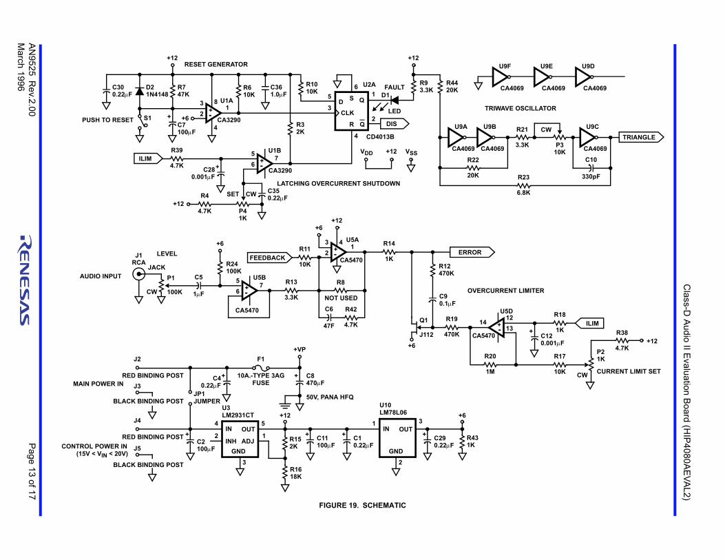
FIGURE 19. SCHEMATIC
3
21+
-
8 U1A
CA32904
+12RESET GENERATOR
R610K
R747K
D21N4148
C300.22F
S1PUSH TO RESETC7100F
+ +6
5
67
U1B
CA3290
+-
LATCHING OVERCURRENT SHUTDOWN
C280.001F
+
SET C350.22F
P41K
4.7K
R4+12
4.7K
R39
R1010K
ILIM
DS Q
CLK
R Q
5
3
6
4
R32K
U2A
DIS2
1
CD4013B
FAULT
LED
D1
R93.3K
+12
R4420K
U9A
CA4069
U9B
CA4069
20K
R22
3.3K
R21
U9F
CA4069
TRIWAVE OSC
6.8
R2
+12VDD VSS
P1
100KCW
JACK
LEVELJ1RCA
AUDIO INPUT C5
1F
+6
R24100K
3
21+
-
4 U5A
CA5470
+12
5
67
U5B
CA5470
+-
FEEDBACK
3.3K
R13
10K
R11
NOT USED
R8
+6
4.7K
R42C6
47F
1K
R14
ERROR
R12470K
C90.1F
Q1
J112
+6
470K
R19 12
1314 +
-
U5D
CA5470
1M
R20
OVERCURRENT LIM
C40.22F
+
F1
10A.-TYPE 3AGFUSE
C8470F
+
50V, PANA HFQ
+VP
J2
RED BINDING POSTMAIN POWER IN
CONTROL POWER IN(15V < VIN < 20V)
BLACK BINDING POST
J3JP1JUMPER
J4
RED BINDING POST
BLACK BINDING POST
J5C2100F
+
U3LM2931CT
IN OUT
GND
4
2
3
5
INH ADJ1
+12
R152K
R1618K
C11100F
+C10.22F
+C290.22F
+IN OUT
GND
1
2
U10
3LM78L06
R431K
+6
C361.0F
CW

AN
95
25R
ev.2
.00
Pa
ge 1
4 of 17
March
199
6
C
lass-D A
udio
II Evalu
ation
Bo
ard
(HIP
40
80A
EV
AL
2)
C220.1F
C331.0F
R323.9/3W
J6+OUTPUT
RED BINDING POST
J6+OUTPUT
BLACK BINDING POST
C14CCOMP
C230.1F
C341.0F
FIGURE 20. SCHEMATIC
+12V
11
12
13
14
15
16
17
18
20
19
10
9
8
7
6
5
4
3
2
1 BHB
HEN
DIS
VSS
OUT
IN+
HDEL
IN-
LDEL
AHB
BHO
BLO
BLS
VDD
BHS
VCC
ALS
ALO
AHS
AHO
HIP4080AILIM
FEEDBACK
ERROR
TRIANGLE
9
108
+-
U5C
CA5470
DIS
+12
C160.22F
D3
UF4002
R35200K
R34200K
C3182F
C130.22F
R31
10
AHO
R30
10
ALO
R28
10
BHOU7 C15
0.22F
D4UF4002
+VP
C170.1F
Q2RFP22N10
Q3RFP22N10
R29
10
BLO
Q4
RFP22N10
Q5
AOUT
RFP22N10
C180.1F
SRCRET
R330.1
3WNI
L2
16.5H
L1
16.5H
C200.1F
C263.9F
L3
11.5H
C210.1F
C273.9F
L4
11.5H
FC = 30kHz
R404.64K, 1%
C240.001F
R2546.4K, 1%R36
4.64K, 1%
+6
R374.64K, 1%
R2646.4K, 1%
C250.001F
R414.64K, 1%
C320.22F
+12V
POWER GNDSIGNAL GND
Class-D Audio II Evaluation Board
(HIP4080AEVAL2)
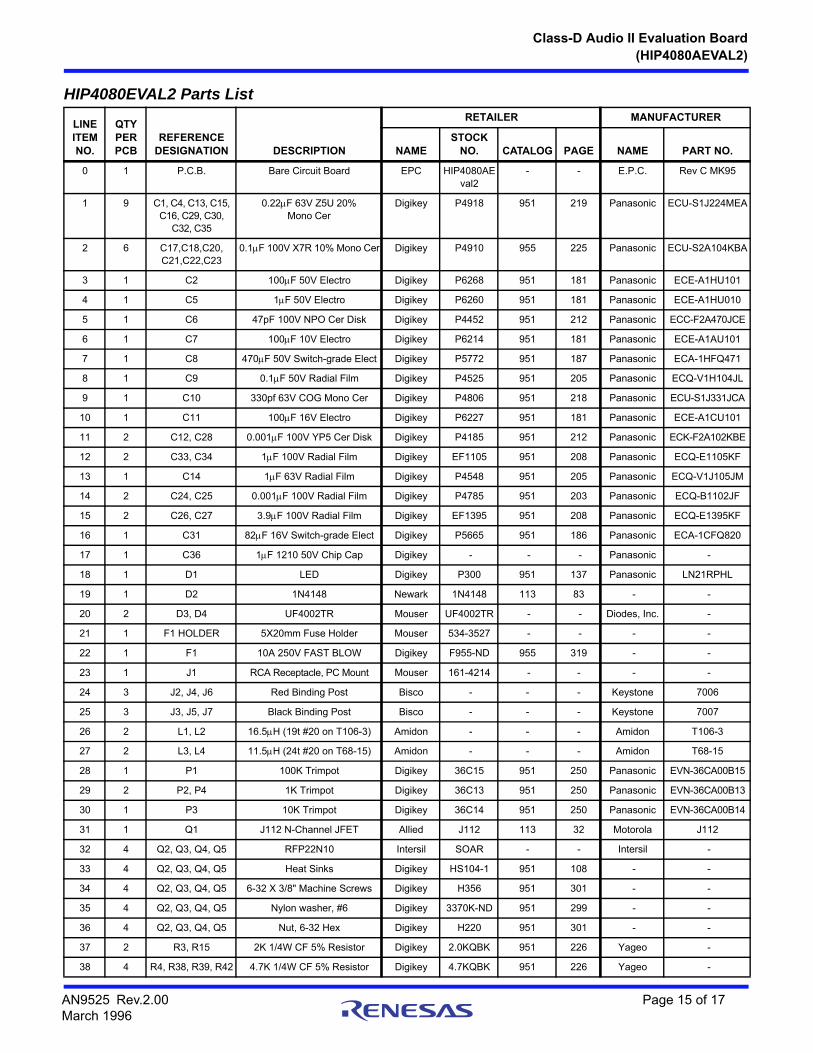
HIP4080EVAL2 Parts List
LINE ITEM NO.
QTY PER PCB
REFERENCEDESIGNATION DESCRIPTION
RETAILER MANUFACTURER
NAMESTOCK
NO. CATALOG PAGE NAME PART NO.
0 1 P.C.B. Bare Circuit Board EPC HIP4080AEval2
- - E.P.C. Rev C MK95
1 9 C1, C4, C13, C15, C16, C29, C30,
C32, C35
0.22F 63V Z5U 20%Mono Cer
Digikey P4918 951 219 Panasonic ECU-S1J224MEA
2 6 C17,C18,C20,C21,C22,C23
0.1F 100V X7R 10% Mono Cer Digikey P4910 955 225 Panasonic ECU-S2A104KBA
3 1 C2 100F 50V Electro Digikey P6268 951 181 Panasonic ECE-A1HU101
4 1 C5 1F 50V Electro Digikey P6260 951 181 Panasonic ECE-A1HU010
5 1 C6 47pF 100V NPO Cer Disk Digikey P4452 951 212 Panasonic ECC-F2A470JCE
6 1 C7 100F 10V Electro Digikey P6214 951 181 Panasonic ECE-A1AU101
7 1 C8 470F 50V Switch-grade Elect Digikey P5772 951 187 Panasonic ECA-1HFQ471
8 1 C9 0.1F 50V Radial Film Digikey P4525 951 205 Panasonic ECQ-V1H104JL
9 1 C10 330pf 63V COG Mono Cer Digikey P4806 951 218 Panasonic ECU-S1J331JCA
10 1 C11 100F 16V Electro Digikey P6227 951 181 Panasonic ECE-A1CU101
11 2 C12, C28 0.001F 100V YP5 Cer Disk Digikey P4185 951 212 Panasonic ECK-F2A102KBE
12 2 C33, C34 1F 100V Radial Film Digikey EF1105 951 208 Panasonic ECQ-E1105KF
13 1 C14 1F 63V Radial Film Digikey P4548 951 205 Panasonic ECQ-V1J105JM
14 2 C24, C25 0.001F 100V Radial Film Digikey P4785 951 203 Panasonic ECQ-B1102JF
15 2 C26, C27 3.9F 100V Radial Film Digikey EF1395 951 208 Panasonic ECQ-E1395KF
16 1 C31 82F 16V Switch-grade Elect Digikey P5665 951 186 Panasonic ECA-1CFQ820
17 1 C36 1F 1210 50V Chip Cap Digikey - - - Panasonic -
18 1 D1 LED Digikey P300 951 137 Panasonic LN21RPHL
19 1 D2 1N4148 Newark 1N4148 113 83 - -
20 2 D3, D4 UF4002TR Mouser UF4002TR - - Diodes, Inc. -
21 1 F1 HOLDER 5X20mm Fuse Holder Mouser 534-3527 - - - -
22 1 F1 10A 250V FAST BLOW Digikey F955-ND 955 319 - -
23 1 J1 RCA Receptacle, PC Mount Mouser 161-4214 - - - -
24 3 J2, J4, J6 Red Binding Post Bisco - - - Keystone 7006
25 3 J3, J5, J7 Black Binding Post Bisco - - - Keystone 7007
26 2 L1, L2 16.5H (19t #20 on T106-3) Amidon - - - Amidon T106-3
27 2 L3, L4 11.5H (24t #20 on T68-15) Amidon - - - Amidon T68-15
28 1 P1 100K Trimpot Digikey 36C15 951 250 Panasonic EVN-36CA00B15
29 2 P2, P4 1K Trimpot Digikey 36C13 951 250 Panasonic EVN-36CA00B13
30 1 P3 10K Trimpot Digikey 36C14 951 250 Panasonic EVN-36CA00B14
31 1 Q1 J112 N-Channel JFET Allied J112 113 32 Motorola J112
32 4 Q2, Q3, Q4, Q5 RFP22N10 Intersil SOAR - - Intersil -
33 4 Q2, Q3, Q4, Q5 Heat Sinks Digikey HS104-1 951 108 - -
34 4 Q2, Q3, Q4, Q5 6-32 X 3/8" Machine Screws Digikey H356 951 301 - -
35 4 Q2, Q3, Q4, Q5 Nylon washer, #6 Digikey 3370K-ND 951 299 - -
36 4 Q2, Q3, Q4, Q5 Nut, 6-32 Hex Digikey H220 951 301 - -
37 2 R3, R15 2K 1/4W CF 5% Resistor Digikey 2.0KQBK 951 226 Yageo -
38 4 R4, R38, R39, R42 4.7K 1/4W CF 5% Resistor Digikey 4.7KQBK 951 226 Yageo -
AN9525 Rev.2.00 Page 15 of 17March 1996

Class-D Audio II Evaluation Board
(HIP4080AEVAL2)
39 4 R36, R37, R40, R41 4.64K 1/4W 1% MF Resist Digikey 4.64QBK 951 226 Yageo -
40 3 R9, R13, R21 3.3K 1/4W 1% MF Resist Digikey 3.3KQBK 951 226 Yageo -
41 4 R6, R10, R11, R17 10K 1/4W CF 5% Resistor Digikey 10KQBK 951 226 Yageo -
42 1 R7 47K 1/4W CF 5% Resistor Digikey 47KQBK 951 226 Yageo -
43 1 R8 NOT INSTALLED - - - - - -
44 2 R25, R26 46.4K 1/4W 1% MF Resist Digikey 46.4KQBK 951 226 Yageo -
45 2 R12, R19 470K 1/4W CF 5% Resistor Digikey 470KQBK 951 226 Yageo -
46 3 R14, R18, R43 1K 1/4W CF 5% Resistor Digikey 1KQBK 951 226 Yageo -
47 1 R16 18K 1/4W CF 5% Resistor Digikey 18KQBK 951 226 Yageo -
48 1 R20 1M 1/4W CF 5% Resistor Digikey 1MQBK 951 226 Yageo -
49 1 R22 20K 1/4W CF 5% Resistor Digikey 20KQBK 951 226 Yageo -
50 1 R23 6.8K 1/4W CF 5% Resistor Digikey 6.8KQBK 951 226 Yageo -
51 1 R24 100K 1/4W CF 5% Resistor Digikey 100KQBK 951 226 Yageo -
52 4 R28, R29, R30, R31 10 1/4W CF 5% Resistor Digikey 10.0QBK 951 226 Yageo -
53 1 R32 3.9 5% 3W Digikey P3.9W-3 951 227 Yageo -
54 1 R33 0.1 3W 5% WW Resistor Digikey SC3D-0.1 951 228 Yageo -
55 2 R34, R35 200K, 1/4W CF 5% Resistor Digikey 200KQBK 951 226 Yageo -
56 1 R44 20K, 1/4W CF 5% Resistor Digikey 20KQBK 951 226 Yageo -
57 1 S1 Push Button Switch Mouser 102-1271 - - C&K 8121SD9AV2GE
58 1 U1 CA3290E Intersil CA3290E SOAR - - -
59 1 U2 CD4013BE Intersil CD4013BE SOAR - - -
60 1 U3 LM2931CT Digikey 9192B-ND 951 89 National -
61 1 U5 CA5470E Intersil CA5470E SOAR - - -
62 1 U7 HIP4080AIP Intersil HIP4080AIP SOAR - - -
63 1 U9 CD4069UBE Intersil CD4069UBE SOAR - - -
64 1 U10 78L06 Voltage Reg. Digikey NJM78L06A - - Motorola -
65 1 SU1 8-pin IC Mach. Screw Sockets Digikey AE7208 951 75 Assmann -
66 3 SU2, SU5, SU9 14-pin IC Mach. Screw Sockets Digikey AE7214 951 75 Assmann -
67 1 SU7 20-pin IC Mach. Screw Sockets Digikey AE7220 951 75 Assmann -
68 4 Standoff Board Standoff Newark 81N2587 113 1226 - -
HIP4080EVAL2 Parts List (Continued)
LINE ITEM NO.
QTY PER PCB
REFERENCEDESIGNATION DESCRIPTION
RETAILER MANUFACTURER
NAMESTOCK
NO. CATALOG PAGE NAME PART NO.
AN9525 Rev.2.00 Page 16 of 17March 1996
http://www.renesas.comRefer to "http://www.renesas.com/" for the latest and detailed information.
Renesas Electronics America Inc.1001 Murphy Ranch Road, Milpitas, CA 95035, U.S.A.Tel: +1-408-432-8888, Fax: +1-408-434-5351Renesas Electronics Canada Limited9251 Yonge Street, Suite 8309 Richmond Hill, Ontario Canada L4C 9T3Tel: +1-905-237-2004Renesas Electronics Europe LimitedDukes Meadow, Millboard Road, Bourne End, Buckinghamshire, SL8 5FH, U.KTel: +44-1628-651-700, Fax: +44-1628-651-804Renesas Electronics Europe GmbHArcadiastrasse 10, 40472 Düsseldorf, Germany Tel: +49-211-6503-0, Fax: +49-211-6503-1327Renesas Electronics (China) Co., Ltd.Room 1709 Quantum Plaza, No.27 ZhichunLu, Haidian District, Beijing, 100191 P. R. ChinaTel: +86-10-8235-1155, Fax: +86-10-8235-7679Renesas Electronics (Shanghai) Co., Ltd.Unit 301, Tower A, Central Towers, 555 Langao Road, Putuo District, Shanghai, 200333 P. R. China Tel: +86-21-2226-0888, Fax: +86-21-2226-0999Renesas Electronics Hong Kong LimitedUnit 1601-1611, 16/F., Tower 2, Grand Century Place, 193 Prince Edward Road West, Mongkok, Kowloon, Hong KongTel: +852-2265-6688, Fax: +852 2886-9022Renesas Electronics Taiwan Co., Ltd.13F, No. 363, Fu Shing North Road, Taipei 10543, TaiwanTel: +886-2-8175-9600, Fax: +886 2-8175-9670Renesas Electronics Singapore Pte. Ltd.80 Bendemeer Road, Unit #06-02 Hyflux Innovation Centre, Singapore 339949Tel: +65-6213-0200, Fax: +65-6213-0300Renesas Electronics Malaysia Sdn.Bhd.Unit 1207, Block B, Menara Amcorp, Amcorp Trade Centre, No. 18, Jln Persiaran Barat, 46050 Petaling Jaya, Selangor Darul Ehsan, MalaysiaTel: +60-3-7955-9390, Fax: +60-3-7955-9510Renesas Electronics India Pvt. Ltd.No.777C, 100 Feet Road, HAL 2nd Stage, Indiranagar, Bangalore 560 038, IndiaTel: +91-80-67208700, Fax: +91-80-67208777Renesas Electronics Korea Co., Ltd.17F, KAMCO Yangjae Tower, 262, Gangnam-daero, Gangnam-gu, Seoul, 06265 KoreaTel: +82-2-558-3737, Fax: +82-2-558-5338
SALES OFFICES
© 2018 Renesas Electronics Corporation. All rights reserved.Colophon 7.0
(Rev.4.0-1 November 2017)
Notice
1. Descriptions of circuits, software and other related information in this document are provided only to illustrate the operation of semiconductor products and application examples. You are fully responsible for
the incorporation or any other use of the circuits, software, and information in the design of your product or system. Renesas Electronics disclaims any and all liability for any losses and damages incurred by
you or third parties arising from the use of these circuits, software, or information.
2. Renesas Electronics hereby expressly disclaims any warranties against and liability for infringement or any other claims involving patents, copyrights, or other intellectual property rights of third parties, by or
arising from the use of Renesas Electronics products or technical information described in this document, including but not limited to, the product data, drawings, charts, programs, algorithms, and application
examples.
3. No license, express, implied or otherwise, is granted hereby under any patents, copyrights or other intellectual property rights of Renesas Electronics or others.
4. You shall not alter, modify, copy, or reverse engineer any Renesas Electronics product, whether in whole or in part. Renesas Electronics disclaims any and all liability for any losses or damages incurred by
you or third parties arising from such alteration, modification, copying or reverse engineering.
5. Renesas Electronics products are classified according to the following two quality grades: “Standard” and “High Quality”. The intended applications for each Renesas Electronics product depends on the
product’s quality grade, as indicated below.
"Standard": Computers; office equipment; communications equipment; test and measurement equipment; audio and visual equipment; home electronic appliances; machine tools; personal electronic
equipment; industrial robots; etc.
"High Quality": Transportation equipment (automobiles, trains, ships, etc.); traffic control (traffic lights); large-scale communication equipment; key financial terminal systems; safety control equipment; etc.
Unless expressly designated as a high reliability product or a product for harsh environments in a Renesas Electronics data sheet or other Renesas Electronics document, Renesas Electronics products are
not intended or authorized for use in products or systems that may pose a direct threat to human life or bodily injury (artificial life support devices or systems; surgical implantations; etc.), or may cause
serious property damage (space system; undersea repeaters; nuclear power control systems; aircraft control systems; key plant systems; military equipment; etc.). Renesas Electronics disclaims any and all
liability for any damages or losses incurred by you or any third parties arising from the use of any Renesas Electronics product that is inconsistent with any Renesas Electronics data sheet, user’s manual or
other Renesas Electronics document.
6. When using Renesas Electronics products, refer to the latest product information (data sheets, user’s manuals, application notes, “General Notes for Handling and Using Semiconductor Devices” in the
reliability handbook, etc.), and ensure that usage conditions are within the ranges specified by Renesas Electronics with respect to maximum ratings, operating power supply voltage range, heat dissipation
characteristics, installation, etc. Renesas Electronics disclaims any and all liability for any malfunctions, failure or accident arising out of the use of Renesas Electronics products outside of such specified
ranges.
7. Although Renesas Electronics endeavors to improve the quality and reliability of Renesas Electronics products, semiconductor products have specific characteristics, such as the occurrence of failure at a
certain rate and malfunctions under certain use conditions. Unless designated as a high reliability product or a product for harsh environments in a Renesas Electronics data sheet or other Renesas
Electronics document, Renesas Electronics products are not subject to radiation resistance design. You are responsible for implementing safety measures to guard against the possibility of bodily injury, injury
or damage caused by fire, and/or danger to the public in the event of a failure or malfunction of Renesas Electronics products, such as safety design for hardware and software, including but not limited to
redundancy, fire control and malfunction prevention, appropriate treatment for aging degradation or any other appropriate measures. Because the evaluation of microcomputer software alone is very difficult
and impractical, you are responsible for evaluating the safety of the final products or systems manufactured by you.
8. Please contact a Renesas Electronics sales office for details as to environmental matters such as the environmental compatibility of each Renesas Electronics product. You are responsible for carefully and
sufficiently investigating applicable laws and regulations that regulate the inclusion or use of controlled substances, including without limitation, the EU RoHS Directive, and using Renesas Electronics
products in compliance with all these applicable laws and regulations. Renesas Electronics disclaims any and all liability for damages or losses occurring as a result of your noncompliance with applicable
laws and regulations.
9. Renesas Electronics products and technologies shall not be used for or incorporated into any products or systems whose manufacture, use, or sale is prohibited under any applicable domestic or foreign laws
or regulations. You shall comply with any applicable export control laws and regulations promulgated and administered by the governments of any countries asserting jurisdiction over the parties or
transactions.
10. It is the responsibility of the buyer or distributor of Renesas Electronics products, or any other party who distributes, disposes of, or otherwise sells or transfers the product to a third party, to notify such third
party in advance of the contents and conditions set forth in this document.
11. This document shall not be reprinted, reproduced or duplicated in any form, in whole or in part, without prior written consent of Renesas Electronics.
12. Please contact a Renesas Electronics sales office if you have any questions regarding the information contained in this document or Renesas Electronics products.
(Note 1) “Renesas Electronics” as used in this document means Renesas Electronics Corporation and also includes its directly or indirectly controlled subsidiaries.
(Note 2) “Renesas Electronics product(s)” means any product developed or manufactured by or for Renesas Electronics.