Introduction and Overview - staff-old.najah.edu and... · Solid State Physics - crystal structure...
8
Material Engineering Vacuum and Thin Film Materials Technology - 10661217 By Dr: Iyad Saadeddin 10661217 - Vacuum and thin film material technology Syllabus • Instructor: Dr. Iyad SAADDDIN • Office: physics department (Room #142460) • Expected Course outcome (Objectives): This course is designed to provide an introduction to the physics and methods used in the production and characterization of thin films. Students will examine what thin films are, their important properties, how they are produced, and how we can characterize them. • Grading: First Exam 20% Second Exam 20% Projects and Presentations 20% Final Exam 40% • Textbooks: The material science of thin films, 2nd ed., 1992. By Milton Ohring
Transcript of Introduction and Overview - staff-old.najah.edu and... · Solid State Physics - crystal structure...
Material Engineering
Vacuum and Thin Film Materials Technology - 10661217
ByDr: Iyad Saadeddin
10661217 - Vacuum and thin film material technologySyllabus
• Instructor: Dr. Iyad SAADDDIN
• Office: physics department (Room #142460)
• Expected Course outcome (Objectives): This course is designed to provide an introduction to the physics and methods used in the production and characterization of thin films. Students will examine what thin films are, their important properties, how they are produced, and how we can characterize them.
• Grading: First Exam 20% Second Exam 20%Projects and Presentations 20% Final Exam 40%
• Textbooks: The material science of thin films, 2nd ed., 1992. By Milton Ohring

10661217 - Vacuum and thin film material technology
Syllabus• Intended topics to be covered
Topic number Topic content sections Physics of thin films
1
Overview of film growth: techniques and physics.Solid State Physics - crystal structure and defects,
packing arrangements, close packed planes, thermodynamic vacancy concentration
1.1 - 1.4
2 Thermodynamics - change in free energy, Ellingham diagrams 1.5
3 Thermodynamics - phase diagrams :one component, triple point, binary solid solution, binary eutectic 1.5
4 Kinetics - Fick's Laws, Diffusion coef, Arrhenius 1.6, 8.1 - 8.2
5 Nucleation and Growth: Homogeneous nucleation, critical radius, nucleation rate 1.7 - 1.8
6 Introduction, Trapping, Capillarity model (heterogeneous nucleation) 5.1 - 5.3
7 Growth modes, island growth, zone models, columnar growth 5.4 - 5.6
8 plasma physics
9 Summary - Deposition parameters and their effects on film growth
10661217 - Vacuum and thin film material technology
Syllabus• Intended topics to be covered
Topic number Topic content sections Film deposition
10 kinetic theory of gasses, flow, substrates, cleaning, vacuum pumps and systems 2
11 basic steps, point vs. surface sources purity, hardware 3.1 - 3.4
12 sputter yield, alloys, heating 3.5 - 3.6
13 methods: dc, RF, magnetron, reactive, ion assisted, ion sources, ion etching 3.7 - 3.8
14 epitaxial films, misfit, strain Ch. 715 reaction types, boundaries and flow 4.1 - 4.516 LPCVD, PECVD, LECVD, MOCVD 4.617 Other deposition techniques

10661217 - Vacuum and thin film material technology
Syllabus• Intended topics to be covered
Topic number Topic content sections Film Characterization
18 overview Ch. 619 imaging techniques Ch. 620 structural techniques Ch. 621 chemical techniques Ch. 622 optical techniques Ch. 623 electro/magnetic techniques Ch. 6
Thin Films properties
24n,k : metals, dielectrics, semiconductors; optics of
transparent films, multiple coatings, effective medium theory
Ch. 11
25
resistance/resistivity- metals, insulators - models, discontinuous films
Hall effect complications, magnetoresistance, magnetic properties
Ch. 10
26 Stoney formula, thermal stress, relaxation Ch. 9Projects Students deliver their projects
presentations Students make a power point presentation
10661217 - Vacuum and thin film material technology
1.1: Introduction and OverviewØ Bulk materials (most engineering materials):
Bulk materials have fixed properties like electrical resistivity, optical properties (transparency, reflectivity, absorbance, …), magnetic properties, mechanical properties, defect types, etc…
* Fixed properties à limited applications
* When thickness decrease below certain limit (becomes thin)àmaterial properties drastically changes
* This is called size effect à change in material properties àincrease in application à designing devices for other applications than that for bulks

10661217 - Vacuum and thin film material technology
Introduction and Overview
Ø Thin films have attractive special properties: different from bulk materials, it may be
* Not fully dense* Under stress* Different defect structures from bulk* Quasi ‐ two dimensional (very thin films)* Strongly influenced by surface and interface effects
Ø Therefore thin films can have a versatile applications so that* devices with thin films occupy less space (thickness of few to 100’s nm)* device fabrication requires less materials à less coast devices.
10661217 - Vacuum and thin film material technology
Introduction and OverviewØWhat are thin films?
* thin = less than 1 μm (from 1 – 100’s of nm)* film = layer of material on a substrateà substrate cab be rigid of flexible
Metal film on glass substrate
Layered films on polyimide flexible foil
10661217 - Vacuum and thin film material technology
Introduction and Overview
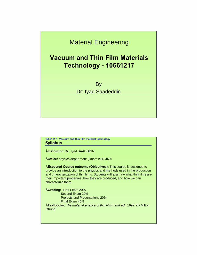
* Flexible Polymer Light Emitting Displays
Ø applications of thin films : very wide range of applications
• Electronics
* thin film FE transistor
10661217 - Vacuum and thin film material technology
Introduction and OverviewØ applications of thin films:
• Optical coating
* Antireflection coating* High-reflection coatings
* Transparent conductive coatings (used in optoelectonic applications)
* UV coating (used in sunglasses)

10661217 - Vacuum and thin film material technology
Introduction and OverviewØ applications of thin films:
• Thin film SQUID (superconducting quantuminterference device) - detect
very low magnetic field
• Magneto – optical films
reading and writing CD-RW
10661217 - Vacuum and thin film material technology
Introduction and OverviewØ applications of thin films:
• Environment & energy technique* low E window glass coating (like electrochromic windows)
• Heat prevention & corrosion resistance

10661217 - Vacuum and thin film material technology
Introduction and OverviewØ applications of thin films:
• Super hard coatings à long-range durability and performance objectives
* So many other applications exist for thin films …….
10661217 - Vacuum and thin film material technology
Introduction and OverviewØ typical steps in making thin films:
1. Emission of particles from source (heat, high voltage , ejection . . .)2. Transport of particles to substrate3. Condensation of particles on substrate

10661217 - Vacuum and thin film material technology
Introduction and OverviewØ thin film deposition methods:
• Two main deposition methods are used today:1) Chemical Vapor Deposition (CVD)Reactant gases introduced in the chamber, chemical reactions occur on wafer surface leading to the deposition of a solid film.E.g. LPCVD, LPCVD, PECVD, most commonly used for dielectrics and Si.
2) Physical Vapor Deposition (PVD) (no chemical reaction involved)Vapors of constituent materials created inside the chamber, and condensation occurs on wafer surface leading to the deposition of a solid film.E.g. evaporation, sputter deposition, most commonly used for metals.
• Other methods that are increasingly gaining importance in film fabrication:1.Coating with a liquid that becomes solid upon heating, e.g. dip coating in a sol gel or spin-on-glass used for planarization.2.Electro-deposition: coating from a solution that contains ions of the species to be coated. E.g. Cu electroplating for global interconnects.3.Thermal oxidation.
10661217 - Vacuum and thin film material technology
Introduction and OverviewØ general characteristics of thin film deposition:
• Deposition rate• Film uniformity: * Across wafer uniformity, * Run-to-run uniformity.• Materials that can be deposited: metal, dielectric, polymer.• Quality of film:
• Physical and chemical properties• Electrical property, breakdown voltage• Mechanical properties, stress and adhesion to substrate• Optical properties, transparency, refractive index• Composition, stoichiometry• Film density, defect (pinhole…) density• Texture, grain size, boundary property, and orientation• Impurity level, doping
• Deposition directionality:• Directional - good for lift-off, trench filling• Non-directional - good for step coverage
• Cost of ownership and operation.

![University of Groningen Properties of High-Frequency Sub … · Ultra Short Pulse Laser Irradiation. Physics Procedia, 12(2), 99-104. ... semiconductors and dielectrics [2 – 5]](https://static.fdocuments.in/doc/165x107/6126a41fcf6a744fa06703ed/university-of-groningen-properties-of-high-frequency-sub-ultra-short-pulse-laser.jpg)

![8.0 Muonium in semiconductors - PSI · Diodes (APD’s) instead of the ... Hyperfine constant for interstitial muonium in semiconductors and dielectrics. ... [8-11 ] (Compare with](https://static.fdocuments.in/doc/165x107/5ac41a327f8b9ae06c8cf990/80-muonium-in-semiconductors-psi-apds-instead-of-the-hyperfine-constant.jpg)


![Fundamentals of a New Sub-Diffraction Direct Laser Writing ...3-dimensional direct laser writing inside material with a s distinct band gap like dielectrics and semiconductors . [22]](https://static.fdocuments.in/doc/165x107/603aa939ba7fc2220e0cd7a3/fundamentals-of-a-new-sub-diffraction-direct-laser-writing-3-dimensional-direct.jpg)