Introducing the Versal Architecture - Xilinx · Pre-Processing, Data Aggregation Complex...
35
© Copyright 2018 Xilinx Presented By Sumit Shah Director of Silicon Product Marketing and Management October 2, 2018 Introducing the Versal Architecture
Transcript of Introducing the Versal Architecture - Xilinx · Pre-Processing, Data Aggregation Complex...

© Copyright 2018 Xilinx
Presented By
Sumit Shah
Director of Silicon Product Marketing and Management
October 2, 2018
Introducing the Versal Architecture

© Copyright 2018 Xilinx
The Technology Conundrum .. And the Need for a New Compute Paradigm
Sensor Fusion,
Pre-Processing,
Data Aggregation
Complex
Algorithms,
Full Linux “Services”
Domain Specific
Parallelism(e.g., Video, ML)
Irregular
data types,
instruction sets,
data operation
Safety Processing,
or Latency-Critical
Workloads
Whole
Application
Processing Architectures
are Not Scaling
A Single Architecture
Can’t Do It Alone
10
100
1000
10,000
100,000 ?
2X / 3.5 Years
2X / 1.5 Years
2X / 6 Years
2X / 3.5 Years
1980 1985 1990 1995 2000 2005 2010 2015
Performancevs. VAZ11-780
CISC
RISC
End of DennardScaling
AmdahlsLaw
40 YEARS OF PROCESSOR PERFORMANCE
Source: John Hennessy and David Patterson, Computer Architecture: A Quantitative Approach, 6/e 2018
>> 2

© Copyright 2018 Xilinx
Need for a New Programming Paradigm
Software DeveloperNeeds Agility and Abstraction
Hardware DeveloperNeeds Flexibility to Optimize for Performance/Power
>> 3
Ecosystem ofLibraries
FamiliarPlatform
Flexible Platform to Optimize for Performance/Power
Need a Scalable, Unified Platform
Modify,Design, Add Code

© Copyright 2018 Xilinx
New Device Category: Adaptive Compute Acceleration Platform
Diverse Workloads in
Milliseconds
Future-Proof for
New Algorithms
ADAPTIVE
AdaptableEngines
ScalarEngines
IntelligentEngines
COMPUTE ACCELERATION
Enabling Data Scientists, SW Developers, HW Developers>> 4
PLATFORM
Development Tools HW/SW Libraries Run-time Stack
SW Programmable Silicon Infrastructure

© Copyright 2018 Xilinx
Introducing the World’s First ACAP
>> 5
˃ Heterogeneous Acceleration
˃ For Any Application
˃ For Any Developer

© Copyright 2018 Xilinx
High-EndGPU
Versal Device
Net
V1 I
mg/S
ec (
<2m
s)
UltraScale+FPGA
VersalDevice
Sin
gle
-Chip
Encry
pte
d T
raff
ic (
Gb/s
)
Breakthrough Performance for Cloud, Network, and Edge
>> 6
>8X
Cloud ComputeBreakthrough AI Inference
NetworkingMulti-terabit Throughput
5G WirelessCompute for Massive MIMO
Edge ComputeAI Inference at Low Power
4X
UltraScale+RFSoC
VersalDevice
Int16x16 D
SP
Com
pute
(T
era
MA
C/
se
c)
5X
UltraScale+MPSoC
VersalDevice
ResN
et5
0 im
g/s
ec (
batc
h=
1)
15X

© Copyright 2018 Xilinx
Adaptable Engines2X compute density
Programmable I/O• Any sensor, any interface
• Extendable peripheral set
Intelligent Engines• AI Compute
• Diverse DSP workloads
DDR Memory• 2X bandwidth/pin
• Server-class density
Protocol Engines• Integrated 600G cores
• 4X encrypted bandwidth
PCIe & CCIX• 2X PCIe & DMA bandwidth
• Cache-coherent interface
to accelerators
Transceivers• Broad range, 25G →112G
• 58G in mainstream devices
Scalar Engines• Platform Control
• Edge Compute
Versal Architecture Overview
>> 7
Network-on-Chip• Guaranteed Bandwidth
• Enables SW Programmability

© Copyright 2018 Xilinx
Platform Management ControllerBringing the Platform to Life & Keeping it Safe & Secure
>> 8
Boot & Configuration
˃ Boots the platform in milliseconds (any engine first)
˃ 8X faster dynamic reconfiguration
˃ Advanced power & thermal management
Security, Safety & Reliability Enclave
˃ HW Root of Trust
˃ Cryptographic acceleration & confidentiality
˃ Enhanced diagnostics, system monitoring & anti-tamper
˃ Error mitigation, detection & management for safety
Integrated Platform Interfaces & High Speed Debug
˃ Integrated flash, system & debug interfaces
˃ High-speed non-invasive, chip-wide debugBOOT & CONFIG
Boot
10s of Milliseconds
DONE
DEBUG SAFETY SECURITY

© Copyright 2018 Xilinx
A Processor in Every DeviceDiverse Use Models for Scalar Processing
>> 9
Edge Compute &
Autonomous Systems
Complex processing
for intelligent edge and endpoint
Operation & Management
in Communication Systems
Board level control monitoring
Control Plane Processing
in the Network & Cloud
Data path management &
device management

© Copyright 2018 Xilinx
The Arm Subsystem
>> 10
Application Processing Unit
ARM® Cortex™-A72
NEON™
Floating Point Unit
48 KB I-Cachew/Parity
32 KBD-Cache w/ECC
MemoryManagement Unit
EmbeddedTrace Macrocell
GIC-520 SCU 1MB L2 w/ECCCCI/SMMU
12
Real Time Processing Unit
ARM® Cortex™-R5
(Split & Lockstep)
Vector Floating Point Unit
Memory Protection Unit
32 KB I-Cache w/ECC 32 KB D-Cache w/ECC
GIC 256KB TCM w/ECC
12
256KB OCM w/ECC
Dual-Core ARM Cortex-A72 Application Processors
˃ Up to 1.7GHz for 2X single-threaded performance1
˃ Cost and power optimized (half the power)
˃ Code compatibility (ARMv8-A architecture)
˃ Enables SW developers to start from a familiar place
1: DMIPS vs. Zynq UltraScale+ MPSoCs
Dual-Core ARM Cortex-R5 Real Processors
˃ Up to 750MHz for 1.4X greater performance1
˃ Low latency and deterministic
˃ Flexible operation modes: Split-Mode and Lock-Step
˃ Highest levels of functional safety (ASIL and SIL)

© Copyright 2018 Xilinx
Adaptable Engines
>> 11
Adaptable
Hardware Engines
Programmable logic for fine-grained
parallel processing, data aggregation,
and sensor fusion
Programmable memory hierarchy
to optimize compute efficiency
High bandwidth, low latency data
movement between engines and I/O

© Copyright 2018 Xilinx
Greater Compute Density for Any Workload
Re-Architected Hardware Fabric
˃ 4X density per logic block for more compute
˃ Less external routing→ greater performance
˃ Code and IP compatible with 16nm devices
Tune for Power & Performance
˃ Three operating voltages to choose from
˃ Balance power/performance for target app
˃ Equivalent to 3 speed grades in one device
Adaptable to any Workload
˃ Bit-level precision (1 → 1,000) for any algorithm
˃ Improves ML efficiency (compression, pruning)
˃ Forward-compatible to lower precision
neural networks, e.g., BNN
VLOW VHIGH
VMID
20% More
Performance
30%Lower
Power
GENOMIC SEQUENCING
VIDEO
TRANSCODING
ML Inference and Optimizations
(e.g., pruning)
For Any Workload
SPEECH
RECOGNITION
>> 12

© Copyright 2018 Xilinx
Intelligent Engines
>> 13
Intelligent Engines
for Diverse Compute
DSP EnginesHigh-precision floating point & low latency
Granular control for customized data paths
AI EnginesHigh throughput, low latency, and power efficient
Ideal for AI inference and advanced signal processing

© Copyright 2018 Xilinx
DSP EnginesVersatility and Granular Control of Data Path
>> 14
Enhanced Compute architecture
˃ Greater than 1GHz of performance
In t8 Dot Product Complex 18x18
32-b i t S ing le Prec is ion
F loat ing Point
Performance Improvement
UltraScale+ 16nm Versal 7nm
Versatility for Wireless, ML, HPC, and more
˃ Integrated FP32, FP16 floating point, INT24 (HPC)
˃ Integrated complex 18x18 operation (wireless, cable access)
˃ Double the performance in INT8 operation (AI inference)
Code Portability for UltraScale+ 16nm designs
˃ Support for legacy IP and LogiCore libraries
˃ Compatibility with SysGen, Model Composer, HLS tools
2.2X 3.3X 3.6X

© Copyright 2018 Xilinx
Intelligent EnginesMassive AI Inference Throughput and Wireless Compute
>> 15
Mem
ory
AI
Core
Mem
ory
AI
Core
Mem
ory
AI
Core
Mem
ory
AI
Core
Mem
ory
AI
Core
Mem
ory
AI
Core
Mem
ory
AI
Core
Mem
ory
AI
Core
Mem
ory
AI
Core
1.3GHz VLIW / SIMD vector processors
˃ Versatile core for ML and other advanced DSP workloads
SW programmable for any developer
˃ C programmable, compile in minutes
˃ Library-based design for ML framework developers
Massive array of interconnected cores
˃ Instantiate multiple tiles (10s to 100s) for scalable compute
Terabytes/sec of interface bandwidth to other engines
˃ Direct, massive throughput to adaptable HW engines
˃ Implement core application with AI for “Whole App Acceleration”

© Copyright 2018 Xilinx
NoC for Ease of Use, Guaranteed Bandwidth, and Power Efficiency
High bandwidth terabit network-on-chip
˃ Memory mapped access to all resources
˃ Built-in arbitration between engines and memory
High Bandwidth, Low Latency, Low power
˃ Guaranteed QoS
˃ 8X power efficiency vs. FPGA implementations
Eases Kernel Placement
˃ Easily swap kernels at NoC port boundaries
˃ Simplifies connectivity between kernels
>> 16

© Copyright 2018 Xilinx
Adaptable Memory HierarchyThe Right Memory for the Right Job
>> 17
AI ENGINES
Scalar Engines Adaptable Engines Intelligent Engines
WORKLOAD1
UltraRAM UltraRAM
UltraRAM UltraRAM
BRAM BRAM BRAM BRAM
BRAM BRAM BRAM BRAM
Arm
Cortex-R5
Cache
TCM
OCM
Arm
Cortex-A72
Cache
HBMPCIe &
CCIX DDRNetwork
Cores
MIPI
LVDS
GPIO
SerDes
Accelerator RAM
WORKLOADN
Block RAM & UltraRAMEmbedded configurable SRAM
(New) Accelerator RAM4 MB sharable across engines
DDR External MemoryDDR4-3200; LPDDR4-4266
HBMIn-package DRAM
Incre
asin
g B
andw
idth
, D
ecre
asin
g D
ensity
LUTRAMDistributed low-latency memory
local data memory
in AI engines
1 Tb/s
10 Tb/s
100 Tb/s
1,000 Tb/s

© Copyright 2018 Xilinx
Introducing the “Integrated Shell”
>> 18
Network on Chip
Scalar Engines Adaptable Engines Intelligent Engines
Versal
Adaptable
HardwareArm
Dual-Core
Cortex-R5
Arm
Dual-Core
Cortex-A72
PMC
AI
Engines
DSP
Engines
112G
58G
32G
PCIe &
CCIX
(w/DMA)
DDR HBMNx100G
Cores
MIPI
LVDS
GPIO
CO
NF
IGU
RA
BLE
, IN
TE
GR
AT
ED
SH
ELL
System
Memory
Host
Connectivity
CPU
‘Shell’: Pre-Built Core Infrastructure & System Connectivity
˃ External host interface
˃ Memory subsystem
˃ Basic interfaces (e.g., JTAG, USB, GbE)
Key Architectural Elements of the Shell
˃ Platform Management Controller (PMC)
˃ Integrated host interfaces: PCIe & CCIX, DMA
˃ Scalable Memory Subsystem: DDR4 & LPRDDR4
˃ Network-on-Chip for connectivity and arbitration
Greater Performance, Device Utilization, and Productivity
˃ More of the platform available for application’s workload(s)
˃ Target application runs faster with less device congestion
˃ Turn-key, pre-engineered timing closure – no debug

© Copyright 2018 Xilinx
Transceivers: Robust and Scalable Connectivity
>> 19
BACKPLANECOPPER CABLE OPTICS
32GNRZ Transceivers
Optimized for latency and power
58GPAM4 Transceivers
Tuned for the latest copper cable,
backplane & optical interfaces
112GPAM4 Transceivers
Industry-leading performance for
copper cable, backplane, optical

© Copyright 2018 Xilinx
Programmable I/O for Any Sensor, Interface, or Memory
>> 20
˃ Different IO types provide a wide range of speeds and voltages
˃ Configure the same I/O for either memory or sensor interfaces per application requirements
DC 400Mb/s 1600Mb/s 3200Mb/s 4266Mb/s
3.2Gb/s MIPI D-PHY8 Mpix Sensors & Displays
1.8V to 3.3V 0.6V to 1.5V
3.2Gb/s DDR4Server Class Density Per Channel
4.2Gb/s LPDDR4 (0.6V)Highest Memory Bandwidth Per Pin
XDIO(High-Speed)
HDIO, MIO(Legacy Standards)
…

© Copyright 2018 Xilinx
Versal Core Series Enables “Smart Cities”Video Surveillance with Machine Learning
NETWORK-ON-CHIP
AI ENGINES
Scalar Engines Adaptable Engines Intelligent Engines
Arm
Dual-Core
Cortex-R5
Arm
Dual-Core
Cortex-A72
>> 21
CUSTOM MEMORY
HIEARCHY
NEURAL NETWORK
RT COMRESSION
VIDEO SCALING /
Compression
32GPCIe & CCIX
(w/DMA)DDR
Multi-Rate
EthernetCustom
I/O
DSP ENGINES
VIDEO
TRANSCODING
MACHINE
LEARNING
Security
AI Engines for Real-Time Image Recognition
License Plate/Facial Recognition
Adaptable Engines Optimize Compute/Watt
Video scaling
Network On Chip and Memory Subsystem
Interconnects memory and compute Engines
DSP Engines for Video Transcode
Scalable for legacy and emerging video formats
, custom memory hierarchy, compression
Host Connectivity and Network Connectivity
Integrated PCIe and Ethernet
Network

© Copyright 2018 Xilinx
Vivado Design Suite
Frameworks
Embedded Run-Time
New Unified Software
Development Environment
AI & DataScientists
Software ApplicationDevelopers
HardwareDevelopers
Embedded Developers
For Any Developer
>> 22
© Copyright 2018 Xilinx
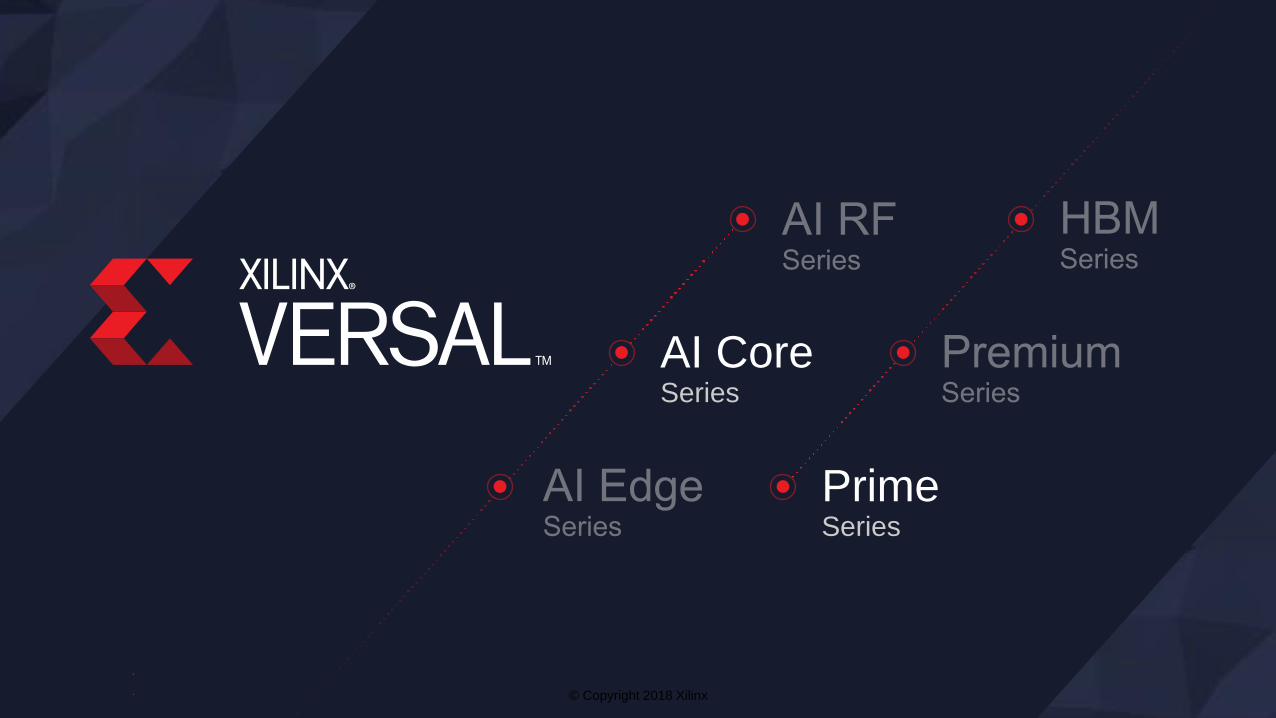
PrimeSeries
AI CoreSeries

© Copyright 2018 Xilinx
DEVICE CATEGORY
FPGA SoC ACAP
FEATURED PRODUCTS
Spartan
Artix
Kintex
Virtex
Zynq-7000
Zynq UltraScale+ MPSoC
Versal
Zynq UltraScale+ RFSoC
Part of the Xilinx Product & Technology Portfolio
>> 24

© Copyright 2018 Xilinx
Announcing the First Two Series of the Versal Portfolio
AI EdgeSeries
AI CoreSeries
Prime SeriesBroad Applicability Across Multiple Markets
˃ Mid-range series in the Versal portfolio
˃ Optimized for connectivity
˃ For in-line acceleration and diverse workloads
AI Core SeriesBreakthrough AI Inference Throughput
˃ Portfolio‘s highest compute and low latency inference
˃ Optimized for cloud, networking, & autonomous applications
˃ For highest range of AI and workload acceleration
HBMSeries
PremiumSeries
PrimeSeries
AI RFSeries
>> 25
© Copyright 2018 Xilinx
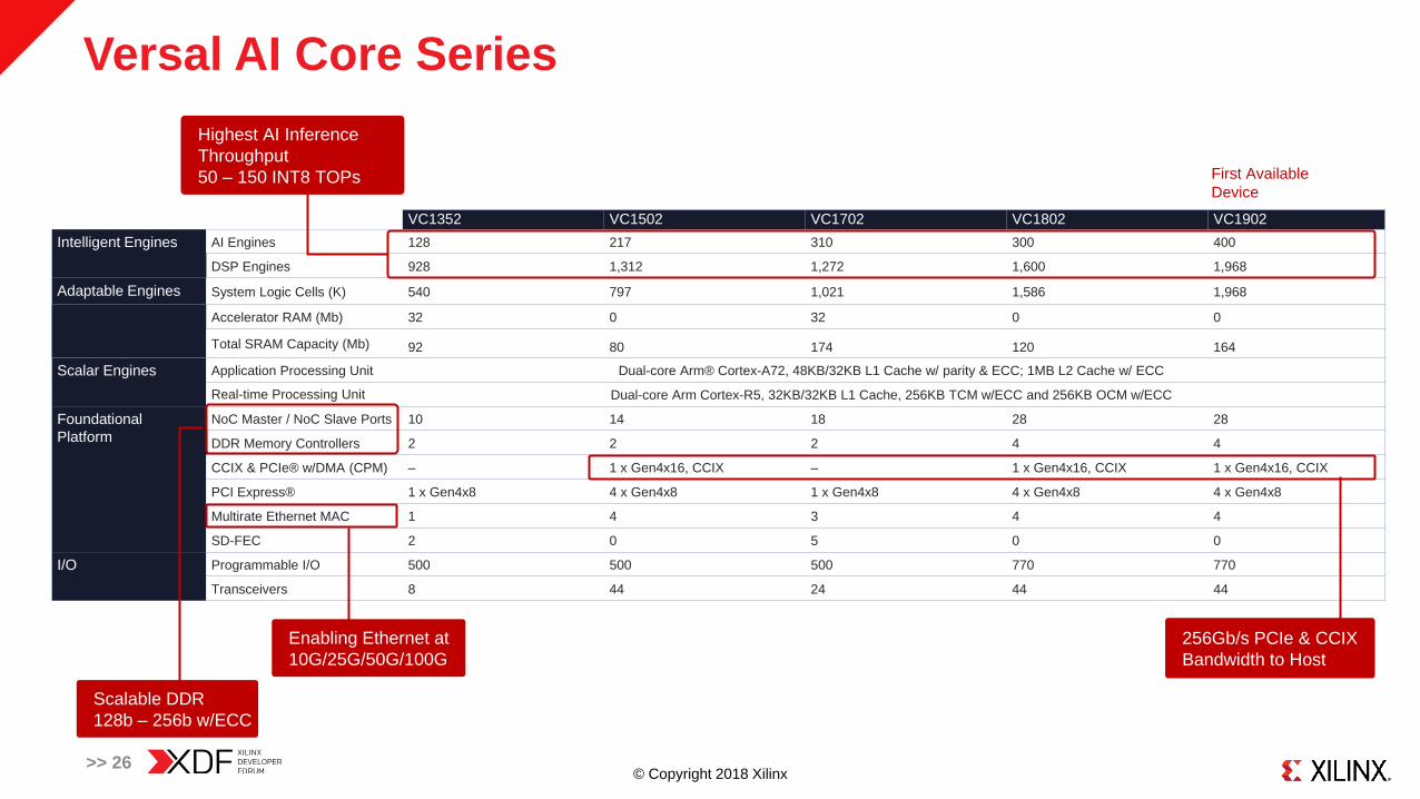
Versal AI Core Series
>> 26
VC1352 VC1502 VC1702 VC1802 VC1902
Intelligent Engines AI Engines 128 217 310 300 400
DSP Engines 928 1,312 1,272 1,600 1,968
Adaptable Engines System Logic Cells (K) 540 797 1,021 1,586 1,968
Accelerator RAM (Mb) 32 0 32 0 0
Total SRAM Capacity (Mb) 92 80 174 120 164
Scalar Engines Application Processing Unit Dual-core Arm® Cortex-A72, 48KB/32KB L1 Cache w/ parity & ECC; 1MB L2 Cache w/ ECC
Real-time Processing Unit Dual-core Arm Cortex-R5, 32KB/32KB L1 Cache, 256KB TCM w/ECC and 256KB OCM w/ECC
Foundational
Platform
NoC Master / NoC Slave Ports 10 14 18 28 28
DDR Memory Controllers 2 2 2 4 4
CCIX & PCIe® w/DMA (CPM) – 1 x Gen4x16, CCIX – 1 x Gen4x16, CCIX 1 x Gen4x16, CCIX
PCI Express® 1 x Gen4x8 4 x Gen4x8 1 x Gen4x8 4 x Gen4x8 4 x Gen4x8
Multirate Ethernet MAC 1 4 3 4 4
SD-FEC 2 0 5 0 0
I/O Programmable I/O 500 500 500 770 770
Transceivers 8 44 24 44 44
Highest AI Inference
Throughput
50 – 150 INT8 TOPs
Scalable DDR
128b – 256b w/ECC
256Gb/s PCIe & CCIX
Bandwidth to Host
Enabling Ethernet at
10G/25G/50G/100G
First Available
Device

© Copyright 2018 Xilinx
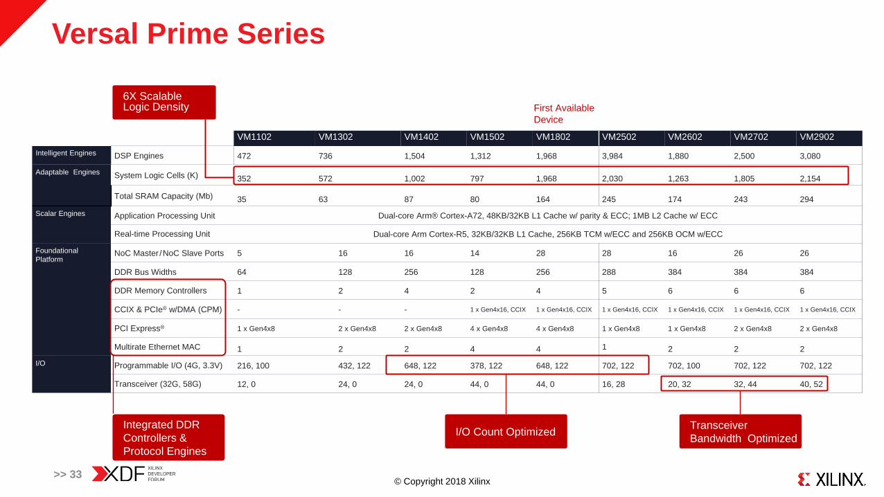
Versal Prime Series
>> 27
VM1102 VM1302 VM1402 VM1502 VM1802 VM2502 VM2602 VM2702 VM2902
Intelligent Engines DSP Engines 472 736 1,504 1,312 1,968 3,984 1,880 2,500 3,080
Adaptable Engines System Logic Cells (K) 352 572 1,002 797 1,968 2,030 1,263 1,805 2,154
Total SRAM Capacity (Mb) 35 63 87 80 164 245 174 243 294
Scalar Engines Application Processing Unit Dual-core Arm® Cortex-A72, 48KB/32KB L1 Cache w/ parity & ECC; 1MB L2 Cache w/ ECC
Real-time Processing Unit Dual-core Arm Cortex-R5, 32KB/32KB L1 Cache, 256KB TCM w/ECC and 256KB OCM w/ECC
Foundational
PlatformNoC Master /NoC Slave Ports 5 16 16 14 28 28 16 26 26
DDR Bus Widths 64 128 256 128 256 288 384 384 384
DDR Memory Controllers 1 2 4 2 4 5 6 6 6
CCIX & PCIe® w/DMA (CPM) - - - 1 x Gen4x16, CCIX 1 x Gen4x16, CCIX 1 x Gen4x16, CCIX 1 x Gen4x16, CCIX 1 x Gen4x16, CCIX 1 x Gen4x16, CCIX
PCI Express® 1 x Gen4x8 2 x Gen4x8 2 x Gen4x8 4 x Gen4x8 4 x Gen4x8 1 x Gen4x8 1 x Gen4x8 2 x Gen4x8 2 x Gen4x8
Multirate Ethernet MAC 1 2 2 4 4 1 2 2 2
I/O Programmable I/O 316 554 770 500 770 824 802 824 824
Transceiver 12 24 24 44 44 44 52 76 92
Integrated DDR
Controllers &
Protocol Engines
Transceiver
Bandwidth OptimizedI/O Count Optimized
6X Scalable Logic Density First Available
Device
© Copyright 2018 Xilinx
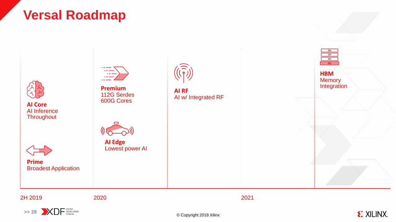
Versal Roadmap
>> 28
2H 2019 2020 2021
HBMMemory Integration
AI EdgeLowest power AI
Premium112G Serdes600G Cores
AI RFAI w/ Integrated RF
AI CoreAI InferenceThroughout
PrimeBroadest Application
© Copyright 2018 Xilinx
Getting Started
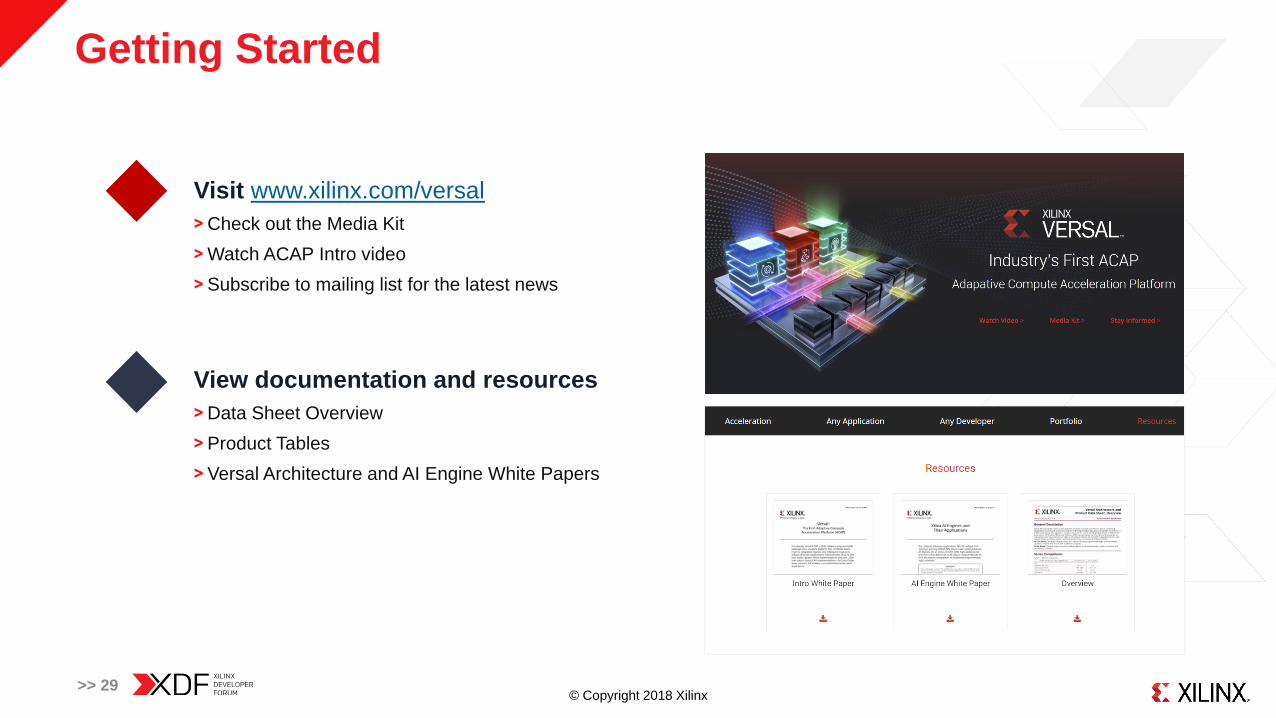
Visit www.xilinx.com/versal
Check out the Media Kit
Watch ACAP Intro video
Subscribe to mailing list for the latest news
View documentation and resources
Data Sheet Overview
Product Tables
Versal Architecture and AI Engine White Papers
>> 29

© Copyright 2018 Xilinx
Key Take-Aways
>> 30
Versal: The First ACAP
Heterogeneous Acceleration
For Any Application
For Any Developer
Announcing Two Families
Versal Prime Series for Broad Application
Versal AI Core Series for Highest AI Throughput
Availability
Early Access Program for SW and tools
Devices Available 2H 2019
© Copyright 2018 Xilinx

© Copyright 2018 Xilinx
Versal AI Core Series
>> 32
VC1352 VC1502 VC1702 VC1802 VC1902
Intelligent Engines AI Engines 128 217 310 300 400
DSP Engines 928 1,312 1,272 1,600 1,968
Adaptable Engines System Logic Cells (K) 540 797 1,021 1,586 1,968
Accelerator RAM (Mb) 32 0 32 0 0
Total SRAM Capacity (Mb) 92 80 174 120 164
Scalar Engines Application Processing Unit Dual-core Arm® Cortex-A72, 48KB/32KB L1 Cache w/ parity & ECC; 1MB L2 Cache w/ ECC
Real-time Processing Unit Dual-core Arm Cortex-R5, 32KB/32KB L1 Cache, 256KB TCM w/ECC and 256KB OCM w/ECC
Foundational
Platform
NoC Master / NoC Slave Ports 10 14 18 28 28
DDR Memory Controllers 2 2 2 4 4
CCIX & PCIe® w/DMA (CPM) – 1 x Gen4x16, CCIX – 1 x Gen4x16, CCIX 1 x Gen4x16, CCIX
PCI Express® 1 x Gen4x8 4 x Gen4x8 1 x Gen4x8 4 x Gen4x8 4 x Gen4x8
Multirate Ethernet MAC 1 4 3 4 4
SD-FEC 2 0 5 0 0
I/O Programmable I/O (4G, 3.3V) 378, 122 378, 122 378, 122 648, 122 648, 122
Transceivers (32G) 8 44 24 44 44
Highest AI Inference
Throughput
50 – 150 INT8 TOPs
Scalable DDR
128b – 256b w/ECC
256Gb/s PCIe & CCIX
Bandwidth to Host
Enabling Ethernet at
10G/25G/50G/100G
First Available
Device
© Copyright 2018 Xilinx
Versal Prime Series
>> 33
VM1102 VM1302 VM1402 VM1502 VM1802 VM2502 VM2602 VM2702 VM2902
Intelligent Engines DSP Engines 472 736 1,504 1,312 1,968 3,984 1,880 2,500 3,080
Adaptable Engines System Logic Cells (K) 352 572 1,002 797 1,968 2,030 1,263 1,805 2,154
Total SRAM Capacity (Mb) 35 63 87 80 164 245 174 243 294
Scalar Engines Application Processing Unit Dual-core Arm® Cortex-A72, 48KB/32KB L1 Cache w/ parity & ECC; 1MB L2 Cache w/ ECC
Real-time Processing Unit Dual-core Arm Cortex-R5, 32KB/32KB L1 Cache, 256KB TCM w/ECC and 256KB OCM w/ECC
Foundational
PlatformNoC Master /NoC Slave Ports 5 16 16 14 28 28 16 26 26
DDR Bus Widths 64 128 256 128 256 288 384 384 384
DDR Memory Controllers 1 2 4 2 4 5 6 6 6
CCIX & PCIe® w/DMA (CPM) - - - 1 x Gen4x16, CCIX 1 x Gen4x16, CCIX 1 x Gen4x16, CCIX 1 x Gen4x16, CCIX 1 x Gen4x16, CCIX 1 x Gen4x16, CCIX
PCI Express® 1 x Gen4x8 2 x Gen4x8 2 x Gen4x8 4 x Gen4x8 4 x Gen4x8 1 x Gen4x8 1 x Gen4x8 2 x Gen4x8 2 x Gen4x8
Multirate Ethernet MAC 1 2 2 4 4 1 2 2 2
I/O Programmable I/O (4G, 3.3V) 216, 100 432, 122 648, 122 378, 122 648, 122 702, 122 702, 100 702, 122 702, 122
Transceiver (32G, 58G) 12, 0 24, 0 24, 0 44, 0 44, 0 16, 28 20, 32 32, 44 40, 52
Integrated DDR
Controllers &
Protocol Engines
Transceiver
Bandwidth OptimizedI/O Count Optimized
6X Scalable Logic Density First Available
Device

© Copyright 2018 Xilinx
Versal AI Core Series
VC1352 VC1502 VC1702 VC1802 VC1902
Intelligent Engines AI Engines 128 217 310 300 400
AI Engine Data Memory Blocks (#) 1024 1736 2480 2400 3200
AI Engine Data Memory (Mb) 32 54.25 77.5 75 100
DSP Engines 928 1,312 1,272 1,600 1,968
Adaptable Engines System Logic Cells (K) 540 797 1,021 1,586 1,968
LUTs 246,784 364,544 466,688 725,000 899,840
Distributed RAM (Mb) 8 11 14 22 27
Memory Total Block RAM (Mb) 18 19 29 28 34
UltraRAM (Mb) 42 60 113 91 130
Accelerator RAM (Mb) 32 0 32 0 0
Total SRAM Capacity (Mb) 92 80 174 120 164
Scalar Engines Application Processing Unit Dual-core Arm® Cortex-A72, 48KB/32KB L1 Cache w/ parity & ECC; 1MB L2 Cache w/ ECC
Real-time Processing Unit Dual-core Arm Cortex-R5, 32KB/32KB L1 Cache, and 256KB TCM w/ECC
Memory 256KB On-Chip Memory w/ECC
Connectivity Ethernet (x2); UART (x2); CAN-FD (x2); USB 2.0 (x1); SPI (x2); I2C (x2)
Foundational Platform NoC Master / NoC Slave Ports 10 14 18 28 28
DDR Bus Width 128 128 128 256 256
DDR Memory Controllers 2 2 2 4 4
CCIX & PCIe® w/DMA (CPM) – 1 x Gen4x16, CCIX – 1 x Gen4x16, CCIX 1 x Gen4x16, CCIX
PCI Express® 1 x Gen4x8 4 x Gen4x8 1 x Gen4x8 4 x Gen4x8 4 x Gen4x8
Multirate Ethernet MAC 1 4 3 4 4
SD-FEC 2 0 5 0 0
Platform Management Controller Boot, Security, Safety, Monitoring, and High Speed Debug
Package Footprint Package Dimensions Ball Pitch XPIO, HDIO, MIO, GTY XPIO, HDIO, MIO, GTY XPIO, HDIO, MIO, GTY XPIO, HDIO, MIO, GTY XPIO, HDIO, MIO, GTY
A1024 31x31 0.92 378, 22, 78, 8 378, 22, 78, 8
E1369 35x35 0.92 378, 44, 78, 8 378, 44, 78, 24
A1596 37.5x37.5 0.92 378, 44, 78, 32 378, 44, 78, 16 378, 44, 78, 32 378, 44, 78, 32
D1760 40x40 0.92 648, 44, 78, 24
A2197 45x45 0.92 378, 44, 78, 44 648, 44, 78, 44 648, 44, 78, 44
© Copyright 2018 Xilinx
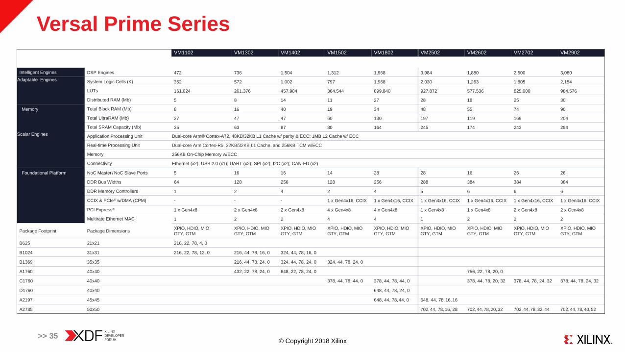
Versal Prime Series
>> 35
VM1102 VM1302 VM1402 VM1502 VM1802 VM2502 VM2602 VM2702 VM2902
Intelligent Engines DSP Engines 472 736 1,504 1,312 1,968 3,984 1,880 2,500 3,080
Adaptable Engines System Logic Cells (K) 352 572 1,002 797 1,968 2,030 1,263 1,805 2,154
LUTs 161,024 261,376 457,984 364,544 899,840 927,872 577,536 825,000 984,576
Distributed RAM (Mb) 5 8 14 11 27 28 18 25 30
Memory Total Block RAM (Mb) 8 16 40 19 34 48 55 74 90
Total UltraRAM (Mb) 27 47 47 60 130 197 119 169 204
Total SRAM Capacity (Mb) 35 63 87 80 164 245 174 243 294
Scalar Engines Application Processing Unit Dual-core Arm® Cortex-A72, 48KB/32KB L1 Cache w/ parity & ECC; 1MB L2 Cache w/ ECC
Real-time Processing Unit Dual-core Arm Cortex-R5, 32KB/32KB L1 Cache, and 256KB TCM w/ECC
Memory 256KB On-Chip Memory w/ECC
Connectivity Ethernet (x2); USB 2.0 (x1); UART (x2); SPI (x2); I2C (x2); CAN-FD (x2)
Foundational Platform NoC Master / NoC Slave Ports 5 16 16 14 28 28 16 26 26
DDR Bus Widths 64 128 256 128 256 288 384 384 384
DDR Memory Controllers 1 2 4 2 4 5 6 6 6
CCIX & PCIe® w/DMA (CPM) - - - 1 x Gen4x16, CCIX 1 x Gen4x16, CCIX 1 x Gen4x16, CCIX 1 x Gen4x16, CCIX 1 x Gen4x16, CCIX 1 x Gen4x16, CCIX
PCI Express® 1 x Gen4x8 2 x Gen4x8 2 x Gen4x8 4 x Gen4x8 4 x Gen4x8 1 x Gen4x8 1 x Gen4x8 2 x Gen4x8 2 x Gen4x8
Multirate Ethernet MAC 1 2 2 4 4 1 2 2 2
Package Footprint Package DimensionsXPIO, HDIO, MIO
GTY, GTM
XPIO, HDIO, MIO
GTY, GTM
XPIO, HDIO, MIO
GTY, GTM
XPIO, HDIO, MIO
GTY, GTM
XPIO, HDIO, MIO
GTY, GTM
XPIO, HDIO, MIO
GTY, GTM
XPIO, HDIO, MIO
GTY, GTM
XPIO, HDIO, MIO
GTY, GTM
XPIO, HDIO, MIO
GTY, GTM
B625 21x21 216, 22, 78, 4, 0
B1024 31x31 216, 22, 78, 12, 0 216, 44, 78, 16, 0 324, 44, 78, 16, 0
B1369 35x35 216, 44, 78, 24, 0 324, 44, 78, 24, 0 324, 44, 78, 24, 0
A1760 40x40 432, 22, 78, 24, 0 648, 22, 78, 24, 0 756, 22, 78, 20, 0
C1760 40x40 378, 44, 78, 44, 0 378, 44, 78, 44, 0 378, 44, 78, 20, 32 378, 44, 78, 24, 32 378, 44, 78, 24, 32
D1760 40x40 648, 44, 78, 24, 0
A2197 45x45 648, 44, 78, 44, 0 648, 44, 78, 16, 16
A2785 50x50 702, 44, 78, 16, 28 702, 44, 78, 20, 32 702, 44, 78, 32, 44 702, 44, 78, 40, 52