
Interface stability in polymer light emitting diodes : a ... · Interface stability in polymer...
148
Interface stability in polymer light emitting diodes : a study with cryogenic ion beam techniques de Jong, M.P. DOI: 10.6100/IR537631 Published: 01/01/2000 Document Version Publisher’s PDF, also known as Version of Record (includes final page, issue and volume numbers) Please check the document version of this publication: • A submitted manuscript is the author's version of the article upon submission and before peer-review. There can be important differences between the submitted version and the official published version of record. People interested in the research are advised to contact the author for the final version of the publication, or visit the DOI to the publisher's website. • The final author version and the galley proof are versions of the publication after peer review. • The final published version features the final layout of the paper including the volume, issue and page numbers. Link to publication General rights Copyright and moral rights for the publications made accessible in the public portal are retained by the authors and/or other copyright owners and it is a condition of accessing publications that users recognise and abide by the legal requirements associated with these rights. • Users may download and print one copy of any publication from the public portal for the purpose of private study or research. • You may not further distribute the material or use it for any profit-making activity or commercial gain • You may freely distribute the URL identifying the publication in the public portal ? Take down policy If you believe that this document breaches copyright please contact us providing details, and we will remove access to the work immediately and investigate your claim. Download date: 19. Jul. 2018
Transcript of Interface stability in polymer light emitting diodes : a ... · Interface stability in polymer...
Interface stability in polymer light emitting diodes : astudy with cryogenic ion beam techniquesde Jong, M.P.
DOI:10.6100/IR537631
Published: 01/01/2000
Document VersionPublisher’s PDF, also known as Version of Record (includes final page, issue and volume numbers)
Please check the document version of this publication:
• A submitted manuscript is the author's version of the article upon submission and before peer-review. There can be important differencesbetween the submitted version and the official published version of record. People interested in the research are advised to contact theauthor for the final version of the publication, or visit the DOI to the publisher's website.• The final author version and the galley proof are versions of the publication after peer review.• The final published version features the final layout of the paper including the volume, issue and page numbers.
Link to publication
General rightsCopyright and moral rights for the publications made accessible in the public portal are retained by the authors and/or other copyright ownersand it is a condition of accessing publications that users recognise and abide by the legal requirements associated with these rights.
• Users may download and print one copy of any publication from the public portal for the purpose of private study or research. • You may not further distribute the material or use it for any profit-making activity or commercial gain • You may freely distribute the URL identifying the publication in the public portal ?
Take down policyIf you believe that this document breaches copyright please contact us providing details, and we will remove access to the work immediatelyand investigate your claim.
Download date: 19. Jul. 2018
Interface stability in polymer light emittingdiodes
A study with cryogenic ion beam techniques
PROEFSCHRIFT
ter verkrijging van de graad van doctoraan de Technische Universiteit Eindhoven,
op gezag van de Rector Magnificus, prof.dr. M. Rem,voor een commissie aangewezen door het College voor Promoties
in het openbaar te verdedigen opdinsdag 17 oktober 2000 om 16.00 uur
door
Machiel Pieter de Jong
geboren te 's-Hertogenbosch
Dit proefschrift is goedgekeurd door de promotoren:
prof.dr. M.J.A. de Voigtenprof.dr. H.H. Brongersma
Copromotor:dr. L.J. van IJzendoorn
Ontwerp omslag: Ben Mobach
Druk: Universiteitsdrukkerij Technische Universiteit Eindhoven
CIP-DATA LIBRARY TECHNISCHE UNIVERSITEIT EINDHOVEN
de Jong, Machiel Pieter
Interface stability in polymer light emitting diodes : a study with cryogenic ion beamtechniques / by Machiel Pieter de Jong. - Eindhoven : Technische UniversiteitEindhoven, 2000. - Proefschrift.ISBN 90-386-1619-8NUGI 812Trefw.: organische halfgeleiders / licht emitterende diodes / grensvlakverschijnselen /ionenbundelanalyseSubject headings: organic semiconductors / molecular electronics / light emitting diodes /interface phenomena / ion beam applications / Rutherford backscattering / radiationeffects


v
Contents
1) Introduction 11.1 Polymer light emitting diodes............................................................1
1.1.1 Operation principles...............................................................11.1.2 The relation between interface stability and device
degradation.............................................................................31.2 Rutherford backscattering spectrometry (RBS) and elastic recoil
detection analysis (ERDA) for pLED characterisation......................41.2.1 Principles of RBS and ERDA................................................ 41.2.2 Ion beam induced damage..................................................... 51.2.3 Damage reduction in cryogenic RBS/ERDA.........................6
1.3 Outline of this thesis.......................................................................... 7References......................................................................................................8
2) The Eindhoven Cryogenic RBS/ERDA Setup (ECRES) 112.1 Introduction........................................................................................112.2 Design criteria....................................................................................11
2.2.1 Sample cooling.......................................................................112.2.2 Sample transfer...................................................................... 122.2.3 Vacuum requirements............................................................ 132.2.4 Requirements for RBS/ERDA experiments...........................15
2.3 Construction of the setup................................................................... 152.3.1 General description................................................................ 152.3.2 The cryocooler....................................................................... 172.3.3 Sample cooling: the sample holder, shrink coupling and
cold shields.............................................................................172.3.4 The analysis chamber.............................................................202.3.5 The load lock..........................................................................232.3.6 The vacuum system................................................................232.3.7 Detector and sample manipulation.........................................25
2.4 Performance of the sample cooling system....................................... 252.5 Summary and conclusions................................................................. 28References......................................................................................................28
3) Reduction of ion beam induced damage in polymers at cryogenictemperatures 293.1 Introduction........................................................................................293.2 Hydrogen loss reduction in poly-(phenylenevinylene)......................30
3.2.1 Sample preparation and ERDA measurements......................303.2.2 Hydrogen loss in room temperature versus cryogenic
vi
measurements.........................................................................313.2.3 Sample heating by the ion beam: the influence of thermal
conductive adhesive, substrate and beam current.................. 333.2.4 Considerations on the shape of the hydrogen loss curve in
cryogenic ERDA measurements............................................ 363.3 Chlorine and hydrogen loss reduction in polyacrylates.....................37
3.3.1 Sample preparation and RBS/ERDA experiments................ 373.3.2 Chlorine and hydrogen loss in room temperature versus
cryogenic measurements........................................................383.4 Damage reduction in model polymer light emitting diodes with
encapsulated polymer films............................................................... 393.4.1 Sample preparation and RBS experiments............................ 393.4.2 Damage in room temperature versus cryogenic RBS
experiments............................................................................403.5 Conclusions........................................................................................44References......................................................................................................44
4) Indium migration in model pLEDs with an ITO anode 474.1 Introduction........................................................................................474.2 The migration of indium into sulfonium precursor-route PPV
deposited on ITO................................................................................494.2.1 Sample preparation and experimental methods..................... 494.2.2 Indium depth distributions measured with RBS.................... 524.2.3 Quantification of precursor residues with PIXE....................564.2.4 Composition of the surface region measured with LEIS and
XPS........................................................................................ 574.2.5 Summary of the results.......................................................... 58
4.3 Indium migration into OC1C10-PPV on ITO, stimulated byannealing or HCl................................................................................ 584.3.1 Sample preparation and experimental methods..................... 584.3.2 Indium and chlorine depth distributions measured with
RBS........................................................................................594.3.3 PIXE, LEIS and XPS measurements..................................... 614.3.4 Summary of the results.......................................................... 61
4.4 The migration of indium into PEDOT:PSS films andPEDOT:PSS/PPV double layers deposited on ITO........................... 614.4.1 Sample preparation and RBS measurements......................... 614.4.2 Indium depth distributions measured with RBS.................... 624.4.3 Summary of the results.......................................................... 68
4.5 Conclusions........................................................................................68References......................................................................................................69
vii
5) Controlled oxidation of the calcium cathode in pLEDs 715.1 Introduction........................................................................................715.2 Oxygen depth profiling in pLEDs using ERDA with pulse shape
discrimination (PSD)......................................................................... 725.3 Intermezzo: separation of pile-up and single events using pulse
shape discrimination.......................................................................... 765.4 Sample preparation............................................................................ 805.5 Electrical and compositional characterisation of the pLEDs.............82
5.5.1 pLEDs without oxidation of the Ca cathode..........................825.5.2 pLEDs with post-deposition oxidised Ca cathodes............... 845.5.3 pLEDs with oxygen exposure during Ca deposition............. 88
5.6 Oxidation caused by the presence of water........................................925.7 Conclusions........................................................................................94References......................................................................................................95
6) Development of an ERDA time-of-flight (TOF) spectrometer 976.1 Introduction........................................................................................976.2 Principles of ERDA-TOF.................................................................. 976.3 Construction of the Eindhoven ERDA-TOF spectrometer................102
6.3.1 General description................................................................ 1026.3.2 The MCP timing detectors..................................................... 1046.3.3 Electronics..............................................................................107
6.4 Performance....................................................................................... 1086.5 Conclusions........................................................................................114References......................................................................................................115
7) The stability of the interface between OC1C10-PPV and PEDOT:PSS 1177.1 Introduction........................................................................................1177.2 Sample preparation and experimental methods................................. 1197.3 Sulphur depth distributions measured with RBS...............................1207.4 Electrical characterisation: degradation effects................................. 1247.5 Discussion and conclusions............................................................... 127References......................................................................................................127
Summary 129
Samenvatting 131
Publications 133
Dankwoord 134
Curriculum Vitae 136

1
1) Introduction
1.1 Polymer light emitting diodes (pLEDs)
1.1.1 Operation principles
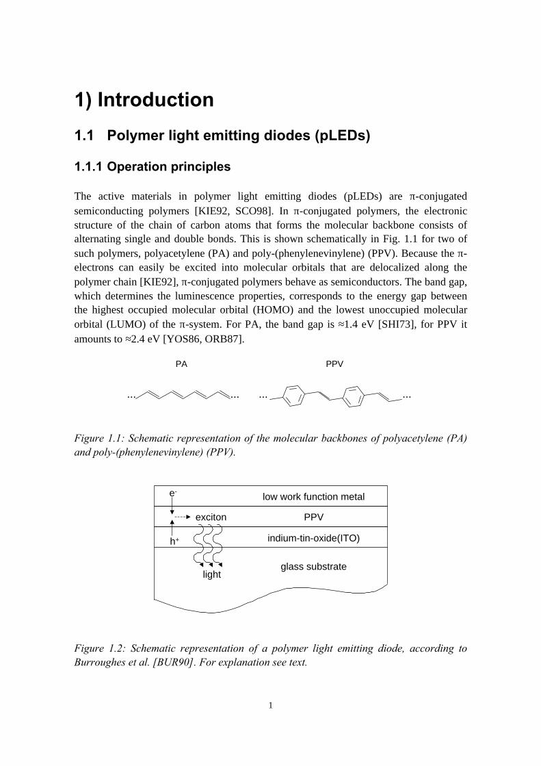
The active materials in polymer light emitting diodes (pLEDs) are π-conjugatedsemiconducting polymers [KIE92, SCO98]. In π-conjugated polymers, the electronicstructure of the chain of carbon atoms that forms the molecular backbone consists ofalternating single and double bonds. This is shown schematically in Fig. 1.1 for two ofsuch polymers, polyacetylene (PA) and poly-(phenylenevinylene) (PPV). Because the π-electrons can easily be excited into molecular orbitals that are delocalized along thepolymer chain [KIE92], π-conjugated polymers behave as semiconductors. The band gap,which determines the luminescence properties, corresponds to the energy gap betweenthe highest occupied molecular orbital (HOMO) and the lowest unoccupied molecularorbital (LUMO) of the π-system. For PA, the band gap is ≈1.4 eV [SHI73], for PPV itamounts to ≈2.4 eV [YOS86, ORB87].
PPVPA
...... ......
Figure 1.1: Schematic representation of the molecular backbones of polyacetylene (PA)and poly-(phenylenevinylene) (PPV).
glass substrate
indium-tin-oxide(ITO)
PPV
low work function metale-
h+
exciton
light
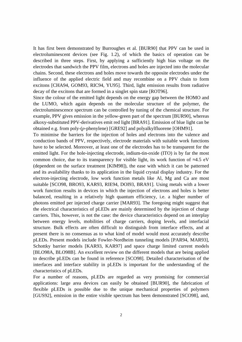
Figure 1.2: Schematic representation of a polymer light emitting diode, according toBurroughes et al. [BUR90]. For explanation see text.
2
It has first been demonstrated by Burroughes et al. [BUR90] that PPV can be used inelectroluminescent devices (see Fig. 1.2), of which the basics of operation can bedescribed in three steps. First, by applying a sufficiently high bias voltage on theelectrodes that sandwich the PPV film, electrons and holes are injected into the molecularchains. Second, these electrons and holes move towards the opposite electrodes under theinfluence of the applied electric field and may recombine on a PPV chain to formexcitons [CHA94, GOM93, RIC94, YU95]. Third, light emission results from radiativedecay of the excitons that are formed in a singlet spin state [ROT96].Since the colour of the emitted light depends on the energy gap between the HOMO andthe LUMO, which again depends on the molecular structure of the polymer, theelectroluminescence spectrum can be controlled by tuning of the chemical structure. Forexample, PPV gives emission in the yellow-green part of the spectrum [BUR90], whereasalkoxy-substituted PPV-derivatives emit red light [BRA91]. Emission of blue light can beobtained e.g. from poly-(p-phenylene) [GRE92] and polyalkylfluorene [OHM91].To minimise the barriers for the injection of holes and electrons into the valence andconduction bands of PPV, respectively, electrode materials with suitable work functionshave to be selected. Moreover, at least one of the electrodes has to be transparent for theemitted light. For the hole-injecting electrode, indium-tin-oxide (ITO) is by far the mostcommon choice, due to its transparency for visible light, its work function of ≈4.5 eV(dependent on the surface treatment [KIM98]), the ease with which it can be patternedand its availability thanks to its application in the liquid crystal display industry. For theelectron-injecting electrode, low work function metals like Al, Mg and Ca are mostsuitable [SCO98, BRO93, KAR93, RIE94, DOI93, BRA91]. Using metals with a lowerwork function results in devices in which the injection of electrons and holes is betterbalanced, resulting in a relatively high quantum efficiency, i.e. a higher number ofphotons emitted per injected charge carrier [MAR93]. The foregoing might suggest thatthe electrical characteristics of pLEDs are mainly determined by the injection of chargecarriers. This, however, is not the case: the device characteristics depend on an interplaybetween energy levels, mobilities of charge carriers, doping levels, and interfacialstructure. Bulk effects are often difficult to distinguish from interface effects, and atpresent there is no consensus as to what kind of model would most accurately describepLEDs. Present models include Fowler-Nordheim tunneling models [PAR94, MAR93],Schottky barrier models [KAR93, KAR97] and space charge limited current models[BLO98A, BLO98B]. An excellent review on the different models that are being appliedto describe pLEDs can be found in reference [SCO98]. Detailed characterisation of theinterfaces and interface stability in pLEDs is important for the understanding of thecharacteristics of pLEDs.For a number of reasons, pLEDs are regarded as very promising for commercialapplications: large area devices can easily be obtained [BUR90], the fabrication offlexible pLEDs is possible due to the unique mechanical properties of polymers[GUS92], emission in the entire visible spectrum has been demonstrated [SCO98], and,
3
last but not least, the production costs for pLEDs are relatively low. However, large scalecommercial application is hindered by the short lifetime of pLEDs. Therefore, it isimportant to study the mechanisms that are responsible for device degradation, such thateventually the stability of pLEDs can be improved.
1.1.2 The relation between interface stability and devicedegradation
Under ambient conditions, the lifetime of pLEDs is extremely short: ranging from a fewseconds to, at best, a few hours. This is due to the fact that both the electroluminescentpolymer and the cathode, which must have a low enough work function to efficientlyinject electrons into the conduction band of the polymer, are sensitive to oxidation. Byencapsulation of pLEDs, and thereby avoiding exposure to air, the lifetime can bedramatically improved. Recently, encapsulated pLEDs have been developed at PhilipsResearch Laboratories of which the operational lifetime exceeds 104 hours.In encapsulated devices, the lifetime is to a large extend limited by the stability of thevarious interfaces. For example, it has been found that oxygen diffusing out of the ITOanode causes oxidation of the electroluminescent polymer [SCO96], which restricts thelifetime of the pLEDs. Additionally, unintentional doping of the polymer by indiumcontaining species originating from the ITO can occur [BRU97]. By introducing anorganic hole-transport layer between the ITO and the emissive polymer, dramatic lifetimeimprovements have been achieved [BER98,KAR96,CAR97], although new problemsmay arise from the introduction of this layer [KIM99]. The interface between the cathodeand the emissive polymer is also problematic. For example, studies by Salaneck et al.[SAL96] have shown that diffusion of low work function metals such as Na, Rb and Cainto electroluminescent polymers occurs already during deposition of the cathode,leading to doping of the polymers. Oxidation of the cathode/polymer interface duringdeposition proved to have a major impact on the interfacial structure and the deviceperformance [SAL96, BRO95], though full understanding of the underlying mechanismswas not reached.Clearly, understanding of the mechanisms and conditions that determine the stability ofinterfaces in pLEDs has to be gained in order to enable the development of more stabledevices in the near future. Therefore, suitable materials analysis techniques are requiredby means of which pLEDs, and interfaces in particular, can be characterised. In section1.2, the applicability of Rutherford backscattering spectrometry (RBS) and elastic recoildetection analysis (ERDA) for this purpose is discussed.
4
1.2 Rutherford backscattering spectrometry (RBS) andelastic recoil detection analysis (ERDA) for pLEDcharacterisation
1.2.1 Principles of RBS and ERDA
By means of Rutherford backscattering spectrometry (RBS) [CHU78] and elastic recoildetection analysis (ERDA) [TES95], which are both ion beam analysis techniques, thedepth distribution of elements in a sample can be measured. Both RBS and ERDA rely onelastic binary collisions between MeV projectile ions and nuclei of atoms in the sample.The MeV ions are produced in a monoenergetic beam by a particle accelerator.In RBS, backscattered ions are detected at a well defined angle. Since the energy transferin an elastic binary collision depends uniquely on the mass ratio of the target nucleus andthe projectile ion, mass identification is possible by measuring the kinetic energy of thebackscattered ions. Due to the fact that MeV ions penetrate into the sample, scatteringtakes place in a depth region that is determined by the range of the projectile ions in thesample material (≈5-10 µm for 2 MeV helium ions). Because the ions lose energythrough interactions with the atoms along their trajectories in the sample [ZIE85], ionsthat are scattered at a certain depth have less kinetic energy than ions that are scattered atthe surface. This implies that measuring the kinetic energy of backscattered ions not onlyprovides a means for mass identification, but also for depth profiling. However, it shouldbe noted that for samples that consist of several layers that contain various elements,ambiguities can occur between the mass of target atoms and their depth in the sample. InRBS experiments with 2 MeV helium ions, the probing depth, i.e. the depth from whichbackscattered ions are still detectable, is typically ≈1-2 µm. For polymer samples, a near-surface depth resolution of ≈10 nm can be achieved.The differential cross section for scattering of a MeV ion in the Coulomb potential of atarget nucleus can be calculated analytically, as was first shown by Ernest Rutherford in1911 [RUT11]. This means that quantitative elemental analysis of samples with RBS isstraightforward, provided that the energy of the projectile ions is such that they fullypenetrate the electron clouds of the target atoms, but do not approach the nuclei at suchclose distances that nuclear forces come into play. Thresholds for both the low and highenergy end of the so-called Rutherford energy regime are given in references [ECU79]and [BOZ91, BOZ92], respectively.Because the kinetic energy of the backscattered particles as well as the differentialscattering cross section increase as the mass of the target atoms increases, RBS is mostsuitable for depth profiling of heavy elements in a light matrix. In contrast to RBS,ERDA is most suitable for depth profiling of light elements in a heavy matrix.In ERDA, target nuclei that recoil from the sample after collisions with projectile ionsare detected. As in RBS, mass identification and depth profiling are possible bymeasuring the kinetic energy of the detected particles. However, a complication of ERDA
5
compared to RBS is that in general recoil species with different masses and scatteredbeam particles are emerging from the sample towards the detection system. Therefore, akey issue in ERDA is the discrimination between the various detected particles.Extensive discussions on the different techniques that are applied to accomplish thisdiscrimination can be found in references [TES95, RIJ93, MAA98]. Two of suchtechniques, ERDA with pulse shape discrimination and ERDA time-of-flight, have beenused in this work and are described in detail in chapters 5 and 6, respectively.In ERDA experiments with 10-20 MeV α-particle beams, as carried out in this work, therecoil cross sections cannot simply be calculated according to Rutherford, due to the factthat 10-20 MeV α-particles approach the target nuclei at such a close distance that theycome within the range of the nuclear force. In this energy regime, the differential crosssection varies erratically with the energy of the α-particles. A significant advantage canbe achieved in this situation, by selecting the beam energy such that a broad maximum isreached in the differential recoil cross section of a certain element, which stronglyimproves the detection sensitivity [IJZ93]. A disadvantage is that calibration samples areusually necessary to guarantee the quantitativity of the measurements. The probing depthin ERDA experiments with 10-20 MeV α-particle beams for the detection of lightelements as C, N, and O is typically 0.1-1 µm.As discussed in section 1.1.2, many problems in pLEDs are related to interface stability,which can often be characterised by measuring the depth distributions of the variouselements that are present in multilayered pLED samples. It can thus be expected that RBSand ERDA are very useful to study processes which are important for the stability ofpLEDs.
1.2.2 Ion beam induced damage
The applicability of RBS and ERDA to polymer samples is limited by ion beam induceddamage. Due to the primary interactions between the impinging ions and the atoms in thepolymer, secondary electrons are produced that subsequently deposit their kinetic energyin a cylindrical volume surrounding the trajectory of the ion, which is called the ion track[KOB68]. As a result, molecular bonds are broken in the ion track, either by the ionsthemselves or by the secondary electrons, and free radicals are formed. In the chemicalreactions that follow the formation of the free radicals, small volatile molecules areformed that subsequently escape from the material [MAR90, CAL92, CAL95, PUG87,JON97, ADE89, MAR97, ABE95]. Mostly hydrogen gas is formed in ion irradiatedpolymers, but also other small molecules like for example C2H2 can be released[CAL92].The release of volatile molecules forms the main limitation for RBS/ERDA experiments:quantitative measurements are hindered by the loss of elements, and depth profiles aredistorted because the energy loss of the impinging ions in the polymer film decreaseswith the atomic areal density in the film. Moreover, in polymer films that are covered bya metal layer, as is the case in pLED samples, gas bubbles can be formed which can
6
totally destroy the samples (see chapter 3). The sensitivity of polymers to ion irradiationdepends strongly on the molecular structure, which means that the degradation effects arenot necessarily very severe in all cases. Indeed, many RBS/ERDA studies on polymersamples have been successfully carried out during the past decades, as is reviewed inreferences [GRE95, SHU92, JON93]. However, ion beam induced degradation can be aserious limitation for the applicability of RBS/ERDA to samples in which the effects ofdegradation are severe, as is expected to be the case for pLEDs.
1.2.3 Damage reduction in cryogenic RBS/ERDA
In RBS/ERDA studies of pLEDs, the outgassing of hydrogen and other volatilemolecules can be expected to cause serious problems, especially because the polymerfilms in pLEDs are covered by a metal layer (electrode) under which gas bubbles can beformed. The outgassing of volatile molecules during ion irradiation of polymer samplescan be strongly reduced by cooling the samples to cryogenic temperatures. By freezingthe volatile species in place, the depth distribution of elements as measured byRBS/ERDA remains intact, even though molecular bonds are still broken in the tracks ofthe impinging ions. It has already been demonstrated that liquid nitrogen cooling cansignificantly reduce the loss of oxygen and chlorine containing molecules in RBS studiesof 1,1,1-trichloroethane (TCE) diffusing into polymethylmethacrylate (PMMA) [MIL86].PMMA is especially sensitive to ion irradiation [CAL92], and room temperatureRBS/ERDA measurements of this polymer are virtually impossible. Liquid nitrogencooling has also been applied by Drew et al., to study the diffusion of deuterated water inpolymers with ion beam techniques [DRE97]. Although liquid nitrogen cooling candecrease the loss of elements like O, N and Cl in ion irradiated polymers, hydrogen lossesare not significantly reduced. Therefore, cooling to temperatures that are much lower than77 K is necessary to avoid problems associated with hydrogen loss.Since there is no data available concerning the outgassing of hydrogen gas from polymersat cryogenic temperatures, the temperature at which hydrogen is effectively trapped inpolymers is estimated by considering (1) the vapour pressure of pure hydrogen as afunction of temperature and (2) data on the release of H2 from photolyzed organicmatrices between 10 and 20 K. The H2 vapour pressure decreases rapidly from ≈100mbar to ≈1 mbar as the temperature is decreased from 20 K to 10 K [HAN74]. Theevaporation of hydrogen from a polymer matrix is undoubtedly reduced compared toevaporation from condensed hydrogen due to the significantly stronger Van der Waalsinteractions with the polymer molecules. Furthermore, studies of UV photolyzed frozenmixtures of CH4, CO, H2O and H2 showed that H2 is only released upon heating between10 and 20 K [HEN82]. It thus can be expected that a sample temperature near 10 K isrequired to suppress hydrogen loss from polymers during RBS/ERDA experiments.Therefore, a cryogenic RBS/ERDA setup has been constructed, with a sample coolingsystem that was designed to ultimately reach a sample temperature near 10 K during themeasurements (see chapter 2).
7
1.3 Outline of this thesis
Chapter 2 deals with the design and construction of the cryogenic RBS/ERDA setup.First, the design criteria with respect to sample cooling, sample transfer, vacuumconditions and RBS/ERDA experiments are defined. Second, a detailed description of thefunctional hardware of the setup is presented. Third, the performance of the samplecooling system is discussed.The reduction of ion beam induced damage in polymer samples during cryogenicRBS/ERDA measurements is discussed in chapter 3. Hydrogen losses in OC1C10-PPVfilms during room temperature and cryogenic ERDA measurements are compared.Attention is paid to sample heating by the ion beam, which depends on the beam current,the heat conductivity of the sample (substrate), and the thermal contact between thesample and the cooling system. Additionally, room temperature versus cryogenicRBS/ERDA measurements of hydrogen/chlorine losses in polyacrylate films arediscussed. The suppression of gas bubble formation in pLED samples in cryogenic RBSmeasurements is also investigated.The stability of the interface between ITO and three different semiconducting polymersin model pLEDs is discussed in chapter 4. For ITO/PPV and ITO/OC1C10-PPV interfaces,the effects of annealing and the presence of hydrochloric acid, which is retained from theconversion of PPV, are investigated. Furthermore, the interface between ITO and poly-(3,4-ethylenedioxithiophene) (PEDOT) doped with poly-(styrenesulfonate) (PSS), whichcan serve as a hole transport layer in pLEDs, is studied after annealing and exposure toair. Due to the hygroscopic and acidic nature of PSS, exposure to air affects the interfacestability.In chapter 5, the controlled oxidation of calcium cathodes in pLEDs is discussed. ThepLEDs were prepared under well controlled conditions, using a glove box integrated withan UHV vapour deposition chamber. The device performance of pLEDs that receiveddifferent oxidation treatments is compared with oxygen depth profiles measured withcryogenic ERDA.The development of an ERDA time-of-flight (TOF) spectrometer is discussed in chapter6. By means of ERDA-TOF, accurate separation between different recoil species ispossible combined with an excellent depth resolution. The extension of the cryogenicRBS/ERDA setup with an ERDA-TOF spectrometer therefore expands the possibilitiesfor depth profiling of light elements in polymer samples.Finally, chapter 7 deals with the stability of the interface between OC1C10-PPV andPEDOT:PSS. By introduction of a PEDOT:PSS hole transport layer between the ITOanode and the emissive polymer, in this case OC1C10-PPV, the problems associated withthe ITO/OC1C10-PPV interface are circumvented. However, new problems can beexpected to arise from the PEDOT:PSS/OC1C10-PPV interface. The interface stabilitywas investigated as a function of annealing, device operation and exposure to air.

8
References
[ABE95] F. Abel, V. Quillet, M. Schott, Nucl. Instr. and Meth B105 (1995) 86[ADE89] M.E. Adel, O. Amir, R. Kalish, L.C. Feldman, J. Appl. Phys. 66 (1989)
3248[BER98] A. Berntsen, Y. Croonen, C. Liedenbaum, H. Schoo, R.J. Visser, J.
Vleggaar, P. van de Weijer, Optical Materials 9 (1998) 125[BLO98A] P.W.M. Blom, M.J.M. de Jong, C.T.H.F. Liedenbaum, Polym. Adv.
Technol. 9 (1998) 390[BLO98B] P.W.M. Blom, M.J.M. de Jong, IEEE Journal of selected topics in
quantum electronics, 4 (1998) 105[BOZ91] M. Bozoian, Nucl. Instr. and Meth. B56/57 (1991) 740[BOZ92] M. Bozoian, Nucl. Instr. and Meth B58 (1992) 127[BRA91] D. Braun, A.J. Heeger, Appl. Phys. Lett. 58 (1991) 1982; erratum, 59
(1991) 878[BRO93] A.R. Brown, J.H. Burroughes, N. Greenham, R.H. Friend, D.D.C.
Bradley, P.L. Burn, A. Kraft, A.B. Holmes, Appl. Phys. Lett. 61 (1993)2793
[BRO95] P. Bröms, J. Birgersson, N. Johnsson, M. Lögdlund, W.R. Salaneck,Synth. Met. 74 (1995) 179
[BRU97] W. Brütting, M.Meier, M. Herold, S. Karg, M. Schwoerer, Chem. Phys.227 (1997) 243
[BUR90] J.H. Burroughs, D.D.C. Bradley, A.R. Brown, R.N. Marks, K. Mackay,R.H. Friend, P.L. Burns, A.B. Holmes, Nature 347 (1990) 539
[CAL92] L. Calcagno, G. Compagnini, G. Foti, Nucl. Instr. and Meth. B65 (1992)413
[CAL95] L. Calcagno, R. Percolla, G. Foti, Nucl. Instr. and Meth. B95 (1995) 59[CAR97] S.A. Carter, M. Angelopoulos, S. Karg, P.J. Brock, and J.C. Scott, Appl.
Phys. Lett. 70 (1997) 2067[CHA94] M. Chandross, S. Mazumdar, S. Jeglinski, X. Wei, Z.V. Vardeny, E.W.
Kwock, T.M. Miller, Phys. Rev. B 50 (19) (1994) 14702[CHU78] W.K. Chu, J.W. Mayer, M.A. Nicolet, Backscattering spectrometry,
(Academic Press, New York, 1978)[DOI93] S. Doi, M. Kuwabara, T. Noguchi, T. Ohnishi, Synth. Met. 55-57 (1993)
4174[DRE97] D.W. Drew, A.S. Clough, P.M. Jenneson, T.E. Shearmur, M.G.D. van der
Grinten, P. Riggs, Nucl. Instr. and Meth. B119 (1997) 429[ECU79] J. L'Ecuyer, J.A. Davies, N. Matsunami, Nucl. Instr. and Meth. 160 (1979)
740[GOM93] P. Gomes da Costa, E.M. Conwell, Phys. Rev. B48 (3) (1993) 1993[GRE92] G. Grem, G. Leditzky, B. Ullrich, G. Leising, Adv. Mater. 4 (1992) 36
9
[GRE95] P.F. Green, B.L. Doyle, Application of ion beam analysis techniques topolymer science, Scattering methods in polymer science, edited by R.W.Richards, (Ellis Horwood, London, 1995)
[GUS92] G. Gustafsson, Y. Cao, G.M. Treacy, F. Klavetter, N. Colaneri, A.J.Heeger, Nature 357 (1992) 477
[HAN74] Handbook of chemistry and physics, edited by R.C. Weast, (CRC Press,Inc., Cleveland, 1974)
[HEN82] L.B. d'Hendecourt, L.J. Allamandola, F. Baas, J.M. Greenberg,Astronomy and Astrofysics 109 (1982) 12
[IJZ93] L.J. van IJzendoorn, H.A. Rijken, S.S. Klein, M.J.A. de Voigt, Appl. Surf.Sci. 70/71 (1993) 58
[JON93] R.A.L. Jones, Ion beam analysis of composition profiles near polymersurfaces and interfaces, Polymer surfaces and interfaces II, edited by W.J.Feast, H.S. Munroe, R.W. Richards, (John Wiley, New York, 1993)
[JON97] M.P. de Jong, A.J.H. Maas, L.J. van IJzendoorn, S.S. Klein, M.J.A. deVoigt, J. Appl. Phys. 82 (1997) 1058
[KAR93] S. Karg, W. Riess, V. Dyakonov, M. Schwoerer, Synth. Met. 54 (1993)427
[KAR96] S. Karg, J.C. Scott, J.R. Salem, and M. Angelopoulos, Synth. Met. 80(1996) 111
[KAR97] S. Karg, M. Meier, W. Riess, J. Appl. Phys. 82 (1997) 1951[KIE92] H. Kiess, Conjugated conducting polymers, (Springer-Verlag, Berlin,
1992)[KIM98] J.S. Kim, M. Granström, R.H. Friend, N. Johansson, W.R. Salaneck, R.
Daik, W.J. Feast, F. Cacialli, J. Appl. Phys. 84 (1998) 6859[KIM99] J.S. Kim, R.H. Friend, F. Cacialli, Appl. Phys. Lett.74 (1999) 3084[KOB68] E.J. Kobetich, R. Katz, Phys. Rev. 170 (1968) 391[MAA98] A.J.H. Maas, Elastic recoil detection analysis with α-particles, (PhD
Dissertation, Eindhoven University of Technology, 1998)[MAR90] G. Marletta, Nucl. Instr. and Meth. B46 (1990) 295[MAR93] R.N. Marks, D.D.C. Bradley, R.W. Jackson, P.L. Burn, A.B. Holmes,
Synth. Met. 57 (1993) 4128[MAR97] C.H.M. Marée, A.M. Vredenberg, F.H.P.M. Habraken, Mater. Chem. and
Phys. 46 (1997) 198[MIL86] P.J. Mills, C.J. Palmstrøm, E.J. Kramer, J. Mater. Sci. 21 (1986) 1479[OHM91] Y. Ohmori, M. Uchida, K. Muro, K. Yoshino, Jpn. J. Appl. Phys. 30
(1991) 1941[ORB87] J. Orbzut, F.E. Karasz, J. Cem. Phys. 87 (1987) 2349[PAR94] I.D. Parker, J. Appl. Phys. 75 (1994) 1656[PUG87] O. Puglisi, A. Licciardello, L. Calcagno, G. Foti, Nucl. Instr. and Meth
B19 (1987) 865[RIC94] M.J. Rice, Y.N. Gartstein, Phys. Rev. Lett. 73 (18) (1994) 2504
10
[RIE94] W. Riess, S. Karg, V. Dyakonov, M. Meier, M. Schwoerer, Synth. Met.60-61 (1994) 906
[RIJ93] H.A. Rijken, Detection methods for depth profiling of light elements usinghigh energy alpha particles, (PhD Dissertation, Eindhoven University ofTechnology, 1993)
[ROT96] L.J. Rothberg, M. Yan, F. Papadimitrakopoulos, M.E. Galvin, T.M.Miller, Synth. Met. 78 (3) (1996) 41
[RUT11] E. Rutherford, Philos. Mag. 21 (1911) 669[SAL96] W.R. Salaneck, S. Strafström, J.L. Brédas, Conjugated polymer surfaces
and interfaces, (Cambridge University Press, Cambridge, 1996)[SCO96] J.C. Scott, J.H. Kaufman, P.J. Brock, R. DiPietro, J. Salem, and J. A.
Goitia, J. Appl. Phys. 79 (1996) 2745[SCO98] T.A. Scotheim, R.L. Elsenbaumer, J. R. Reynolds, Handbook of
conducting polymers, (Marcel Dekker, Inc., New York, 1998)[SHI73] H. Shirakawa, T. Ito, S. Ikeda, Polym. J. 4 (1973) 1973[SHU92] K.R. Shull, Forward recoil spectrometry of polymer interfaces, Physics of
polymer surfaces and interfaces, edited by I.C. Sanchez, (Butterworth-Heinemann, Boston, 1992)
[TES95] J.R. Tesmer, M. Nastasi, Handbook of modern ion beam materialsanalysis, (Materials Research Society, Pittsburg, 1995)
[WES85] R.A. Wessling, J. Polym. Sci., Polym. Symp. 72 (1985) 55[YOS86] K. Yoshino, T. Kakiguchi, S. Hayashi, D.H. Park, R.I. Sugimoto, Jpn. J.
Appl. Phys. 25 (1986) 881[YU95] Z.G. Yu, R.T. Fu, C.Q. Wu, X. Sun, K. Nasu, Phys. Rev. B52 (7) (1995)
4849[ZIE85] J.F. Ziegler, J.P. Biersack, U. Littmark, The stopping and range of ions in
solids, (Pergamon Press, New York, 1985)
11
2) The Eindhoven Cryogenic RBS/ERDASetup (ECRES)
related publications:"High energy ion beam analysis on polymers at cryogenic temperatures" by M.P. deJong, L.J. van IJzendoorn, M.J.A. de Voigt, Nucl. Instr. and Meth. B161-163 (2000) 207-210P.Brinkgreve, to be published
2.1 Introduction
This chapter concerns the design and construction of the cryogenic RBS/ERDA setup,which were carried out in co-operation with P. Brinkgreve, affiliated to the CentralDesign and Engineering Facilities of Eindhoven University of Technology. Section 2.2deals with the design criteria, starting with the choice of a suitable cryocooler.Subsequently the requirements for sample transfer, vacuum properties and RBS/ERDAexperiments are defined. The construction of the setup is discussed in detail in section2.3. Special attention is given to the sample cooling system and the functional hardwareinstalled in and on the analysis chamber and the load lock. The vacuum equipment aswell as the detector and sample positioning system are also described. Finally, theperformance of the sample cooling system is discussed in section 2.4.
2.2 Design criteria
2.2.1 Sample cooling
To reach a sample temperature near 10 K during RBS/ERDA measurements, the samplecooling system must have at least enough cooling power at 10 K to compensate for theheat load of the ion beam, and the samples must be sufficiently screened from the 300 Kenvironment by a cold shield. The heat load L of the ion beam given by CIEL /⋅= , inwhich E is the beam energy, I is the beam current and C is the charge state of the ions. IfE is in MeV and I in µA, then L is in W. With our AVF-cyclotron, RBS/ERDAexperiments can be performed with 2-4 MeV He+ beams and 4-20 MeV He++ beams, witha maximum beam current of 0.1 µA. The heat load therefore will be 1 W or less.One of the most suitable classes of laboratory cryocoolers that operate at 10 K with acooling power of the order of 1 W are commercially available Gifford-McMahon closedcycle helium gas coolers [WAL83]. Gifford-McMahon cryocoolers have some importantadvantages over other expansion cycle systems: all valves and sliding seals operate atroom temperature, and simple but effective regenerative heat exchangers are used. A
12
disadvantage of the Gifford-McMahon cycle is the relatively low efficiency in terms ofwork input per cooling power. Considering also other factors like dimensions, price, andmaintenance we chose a Gifford-McMahon cryocooler manufactured by APD cryogenicsInc. with a cooling power of 2 W at 10 K, model Displex®204-SL [APD]. Thiscryocooler operates in two expansion stages. The first expansion stage, with a coolingpower of 14 W at 80 K, can be used to cool a cold shield that is required to screen thesamples as much as possible from the 300 K environment. The second expansion stage,with 2 W at 10 K, can be used to cool the samples themselves. The cryocooler isdiscussed in more detail in section 2.2.2.The cold shield has to be constructed such that the samples are optimally screenedwithout limiting RBS/ERDA experiments, which require a line of sight from -90º to 90ºwith respect to the sample normal to allow for all possible scattering geometries in theplane formed by the ion beam and the sample normal. The area of the cold shield islimited by the heat absorption due to the 300 K radiation. The heat absorption dependsstrongly on the reflectivity of the cold shield, which again depends on the smoothnessand cleanness of the surface. For very smooth, clean surfaces the heat absorption in a 300K environment is about 10 W/m2 [SUU89]. To make sure that the maximum coolingpower is available at the second stage, the heat load at the first stage should be at least anorder of magnitude lower than the specified 14 W at 80 K, i.e. less than 1 W. Therefore,the area of the cold shield should be smaller than 0.1 m2.
2.2.2 Sample transfer
Sample transfer through a load lock is desired for two reasons. First, to maintain asufficiently low base pressure in the analysis chamber, which is only possible if thechamber does not have to be vented each time that samples are exchanged. Second, toenable sample transfer from a remote glove box to the setup without exposing thesamples to air. This is very important for the analysis of polymer LEDs, which are verysensitive to air.The requirement of sample transfer through a load lock has major implications for thedesign of the sample holder and the way it should be mounted on the cryocooler. On theone hand, a firm coupling between the sample holder and the cryocooler is desired toobtain a good thermal contact. On the other hand, the sample holder should beexchangeable without using much force, due to the fact that load lock systems make useof magnetic transfer rods. However, a firm contact is only desired at low temperatures,which offers the possibility to use a shrink coupling [BER94].Using a shrink coupling between the sample holder and the cryocooler implies that thesample holder cannot be dismounted without heating up the system. Therefore, thesample holder should be constructed such that it can hold several samples at once. In atypical experimental run, of 5 to 20 hours, the number of samples that can be analysedlies, in most cases, somewhere between one and ten. Considering that the size of the
13
sample holder should be kept as small as possible to minimise temperature gradients, wechose to design a sample holder with six sample positions.
2.2.3 Vacuum requirements
At 10 K the sticking coefficient for all residual gases other than He is very close to one[SUU89], resulting in efficient deposition of residual gas on the sample surface. InRBS/ERDA experiments, a film of residual gas covering the samples should not growthicker than a few times 1016 atoms/cm2, which corresponds to several keV energy lossfor 2 MeV He+ ions in glancing angle RBS/ERDA geometries. In some cases,RBS/ERDA experiments need several hours of measurement time, i.e. 104 s. As a rule ofthumb, the maximum allowable deposition rate can thus be set to 1012 molecules⋅s1⋅cm2
for small molecules.The deposition rate of residual gas molecules on a cold surface with sticking coefficient 1can be calculated as:
mkT
pA=
dtdN
π2 , (2.1)
where dN/dt is the number of molecules per unit time, p is the pressure, A is the area ofthe surface, m is the molecular mass, k is Bolzmann's constant and T is the temperature ofthe gas. Assuming the residual gas to be mainly hydrogen, which is a worst case scenariowith respect to the deposition rate, the molecular mass is 3.32⋅1027 kg and the depositionrate for a residual gas temperature of 293 K is about 1021⋅p molecules⋅s1⋅cm2, with p inmbar. The residual gas deposition can be divided in separate contributions arising fromthe analysis chamber and the beam line, which are discussed in the following.It should be noted that the cold shield (see section 2.2.1) screens the samples fromresidual gas in the analysis chamber, which reduces the deposition rate. Residual gasdeposition from within the volume enclosed by the cold shield can be neglected, since themolecules always have to desorb from a cold (<80 K) surface to reach the sample surface.When a cylindrical cold shield is considered, with a slit over half of the circumference toprovide a line of sight between the sample and the RBS/ERDA detectors, the residual gasdeposition through this slit can be estimated as follows. For a cold shield with radius rand a slit width w, the deposition rate is ≈1021⋅p⋅w/r molecules⋅s1⋅cm2, with p, thepressure in the analysis chamber outside the cold shield, in mbar. The slit width should besmall compared to the radius in order to screen the sample as much as possible: w/r≈0.1.The deposition rate arising from the volume outside the cold shields can thus beestimated as 1020⋅p.Since the pressure in the beam guidance system of the cyclotron is 105 mbar, the beamline that connects the setup to the beam guidance system has to be divided in at least twodifferentially pumped sections separated by pumping restrictions (see Fig. 2.1) to reach asufficiently low base pressure in the analysis chamber. Due to the long mean free path ofthe residual gas molecules, also a contribution to the deposition originates from the beam
14
line sections along the line of sight to the sample. The contribution to the deposition ofresidual gas from each section in the beam line depends on the molecular flux through thepumping restrictions, which are narrow tubes with cross section APR. Consider aninfinitesimal area on the sample surface dAs. The number of molecules per unit time thatreach dAs through APR can be approximated by:
222 ldA
mkT
pA=
dtdN sPR
ππ , (2.2)
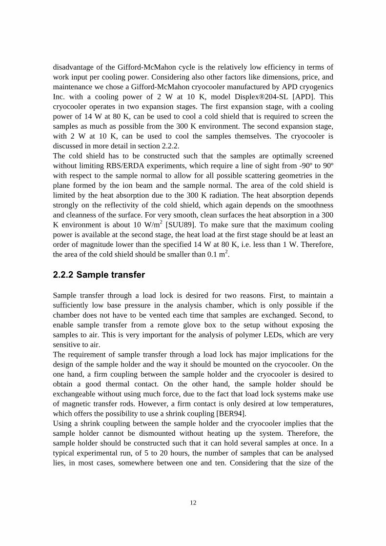
where l is the distance between the sample and APR. The solid angle fraction dAs/(2πl2)determines which fraction of the total molecular flux through APR moves towards dAs. Toestimate the residual gas deposition as a function of the pressure in the differentialpumping sections, the dimensions of the pumping restrictions and the distances betweenthe pumping restrictions and the sample have to be defined. Trading of flow resistance,beam transport properties and ease of handling, tubes with a diameter of 2 cm and 40 cmin length have proven to be a good compromise in the ion channelling beam line at EUT[DIJ97]. Realistic assumptions for the distances between the two pumping restrictionsand the sample are 0.5 m and 2 m, respectively. Again assuming the residual gas to bemainly hydrogen, the deposition rate in molecules⋅s1⋅cm2 is given by 5⋅1016⋅p⋅l2, with pin mbar and l in m.If we demand that each separate contribution to the total deposition rate should be of theorder of 1011 molecules⋅s1⋅cm2, the pressure in the analysis chamber should be 10-9 mbarand the pressure in beam line sections 1 and 2 should be 105 and 107 mbar, respectively.
analysis chamberbeam line section 2 beam line section 1
pumpingrestriction
pumpingrestriction
crosssection Apr
sample
Figure 2.1: The analysis chamber with differentially pumped beam line.
detector
ionbeam
samplesample
170°
30°15°
ionbeam
detector
A B
Figure 2.2: Example of a scattering geometry for RBS experiments (A) and ERDAexperiments (B).
15
2.2.4 Requirements for RBS/ERDA experiments
Two particle detectors must be mountable in the analysis chamber for simultaneous RBSand ERDA experiments. To cover all possible scattering geometries, the detectors mustbe rotatable over 180° with respect to the ion beam. Furthermore, the sample must berotatable over 90°. Two examples of commonly used scattering geometries forRBS/ERDA experiments are shown in Fig. 2.2.When high near surface depth resolution is desired, RBS/ERDA experiments require aglancing angle α of a few degrees between the scattered beam towards the detector andthe sample surface. Especially for such small angles, the measured energy losscorresponding to a certain depth in the sample is a strong function of α and a change of0.1° produces noticeable changes in the spectra. Therefore, the rotation of the detectorsand the sample must be adjustable with an accuracy of 0.1°.Considering that the area of a typical sample is 1 cm2, the beam spot on the sample has tobe 2x2 mm or smaller to allow for glancing angle experiments with an angle of 15°between the ion beam and the sample surface. To obtain a 2x2 mm beam spot withsufficient intensity, magnetic quadrupole lenses have to be present in the beam line tofocus the ion beam. Furthermore, adjustable diaphragms are necessary to ensure a welldefined beam spot size. Focusing the ion beam with magnetic quadrupole lenses causes aspreading in the angle of incidence of the beam, which depends strongly on the distance dbetween the quadrupole lenses and the sample. Assuming a broad beam with a diameterof 2 cm at the location of the quadrupole lenses, the spreading in the angle of incidencewhen the beam is focused to a small spot can be estimated as 2/d⋅57°, with d in cm.Realistic values for d range from 1 to 4 m, which means that an angular spread of a fewtimes 0.1° can be expected. To decrease the angular spread to 0.1°, the beam has to becropped with the adjustable diaphragms.The intensity and the size of the beam must be monitored while adjusting the settings ofthe beam guidance system and the quadrupoles and diaphragms in the beam line. Thiscan be done by placing a diaphragm at the sample position and comparing the relativebeam currents that pass through and impinge on the diaphragm. As a final requirement,beam dose measurements must be possible for quantitative RBS/ERDA measurements.
2.3 Construction of the setup
2.3.1 General description
The setup consists of three main parts: the beam line, the analysis chamber and the loadlock (see Fig. 2.3). The beam line contains a magnetic quadrupole doublet and two slitsets, to focus and crop the ion beam, respectively. The slit sets are made of four jaws thatdefine a square diaphragm. Each jaw can be translated by remote control with anaccuracy of 0.1 mm. A pumping restriction divides the beam line into two differentially
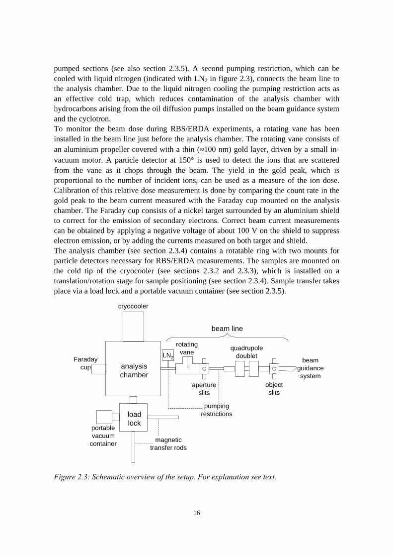
16
pumped sections (see also section 2.3.5). A second pumping restriction, which can becooled with liquid nitrogen (indicated with LN2 in figure 2.3), connects the beam line tothe analysis chamber. Due to the liquid nitrogen cooling the pumping restriction acts asan effective cold trap, which reduces contamination of the analysis chamber withhydrocarbons arising from the oil diffusion pumps installed on the beam guidance systemand the cyclotron.To monitor the beam dose during RBS/ERDA experiments, a rotating vane has beeninstalled in the beam line just before the analysis chamber. The rotating vane consists ofan aluminium propeller covered with a thin (≈100 nm) gold layer, driven by a small in-vacuum motor. A particle detector at 150° is used to detect the ions that are scatteredfrom the vane as it chops through the beam. The yield in the gold peak, which isproportional to the number of incident ions, can be used as a measure of the ion dose.Calibration of this relative dose measurement is done by comparing the count rate in thegold peak to the beam current measured with the Faraday cup mounted on the analysischamber. The Faraday cup consists of a nickel target surrounded by an aluminium shieldto correct for the emission of secondary electrons. Correct beam current measurementscan be obtained by applying a negative voltage of about 100 V on the shield to suppresselectron emission, or by adding the currents measured on both target and shield.The analysis chamber (see section 2.3.4) contains a rotatable ring with two mounts forparticle detectors necessary for RBS/ERDA measurements. The samples are mounted onthe cold tip of the cryocooler (see sections 2.3.2 and 2.3.3), which is installed on atranslation/rotation stage for sample positioning (see section 2.3.4). Sample transfer takesplace via a load lock and a portable vacuum container (see section 2.3.5).
analysischamber
loadlock
portablevacuum
containermagnetic
transfer rods
cryocooler
Faradaycup
beam line
objectslits
apertureslits
quadrupoledoublet
rotatingvaneLN2
pumpingrestrictions
beamguidancesystem
Figure 2.3: Schematic overview of the setup. For explanation see text.
17
high-pressuregas inlet
low-pressuregas return
electricalfeedthroughs
first expansionstage
second expansionstage
flange
thermocouple/heaterwires
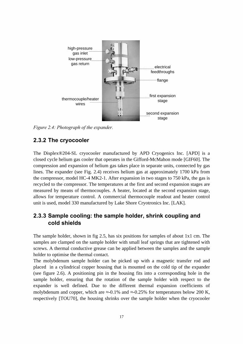
Figure 2.4: Photograph of the expander.
2.3.2 The cryocooler
The Displex®204-SL cryocooler manufactured by APD Cryogenics Inc. [APD] is aclosed cycle helium gas cooler that operates in the Gifford-McMahon mode [GIF60]. Thecompression and expansion of helium gas takes place in separate units, connected by gaslines. The expander (see Fig. 2.4) receives helium gas at approximately 1700 kPa fromthe compressor, model HC-4 MK2-1. After expansion in two stages to 750 kPa, the gas isrecycled to the compressor. The temperatures at the first and second expansion stages aremeasured by means of thermocouples. A heater, located at the second expansion stage,allows for temperature control. A commercial thermocouple readout and heater controlunit is used, model 330 manufactured by Lake Shore Cryotronics Inc. [LAK].
2.3.3 Sample cooling: the sample holder, shrink coupling andcold shields
The sample holder, shown in fig 2.5, has six positions for samples of about 1x1 cm. Thesamples are clamped on the sample holder with small leaf springs that are tightened withscrews. A thermal conductive grease can be applied between the samples and the sampleholder to optimise the thermal contact.The molybdenum sample holder can be picked up with a magnetic transfer rod andplaced in a cylindrical copper housing that is mounted on the cold tip of the expander(see figure 2.6). A positioning pin in the housing fits into a corresponding hole in thesample holder, ensuring that the rotation of the sample holder with respect to theexpander is well defined. Due to the different thermal expansion coefficients ofmolybdenum and copper, which are ≈-0.1% and ≈-0.25% for temperatures below 200 K,respectively [TOU70], the housing shrinks over the sample holder when the cryocooler
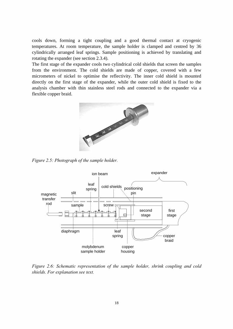
18
cools down, forming a tight coupling and a good thermal contact at cryogenictemperatures. At room temperature, the sample holder is clamped and centred by 36cylindrically arranged leaf springs. Sample positioning is achieved by translating androtating the expander (see section 2.3.4).The first stage of the expander cools two cylindrical cold shields that screen the samplesfrom the environment. The cold shields are made of copper, covered with a fewmicrometers of nickel to optimise the reflectivity. The inner cold shield is mounteddirectly on the first stage of the expander, while the outer cold shield is fixed to theanalysis chamber with thin stainless steel rods and connected to the expander via aflexible copper braid.
Figure 2.5: Photograph of the sample holder.
firststage
secondstage
cold shields
copperhousing
molybdenumsample holder
diaphragm
sample
copperbraid
magnetictransfer
rod
leafspring
ion beam
screw
leafspring
slit
expander
positioningpin
Figure 2.6: Schematic representation of the sample holder, shrink coupling and coldshields. For explanation see text.
19
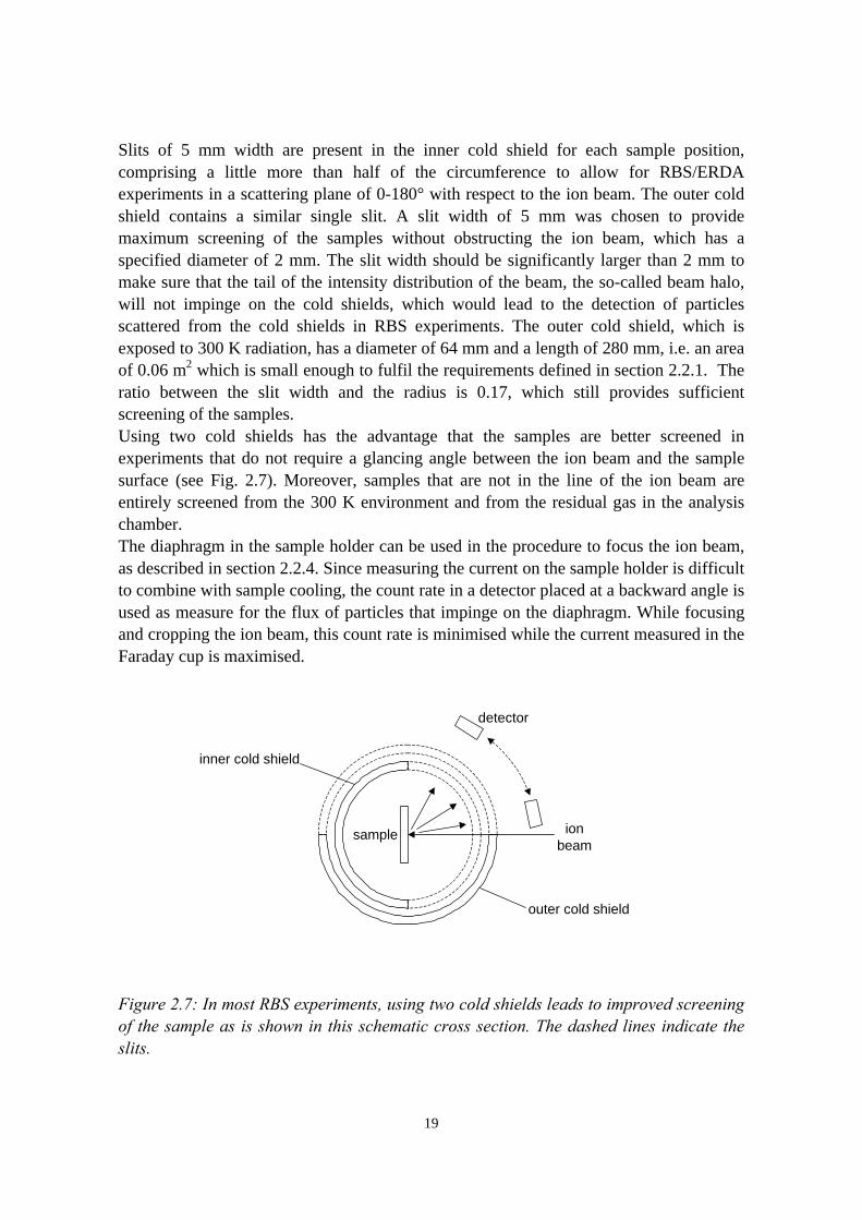
Slits of 5 mm width are present in the inner cold shield for each sample position,comprising a little more than half of the circumference to allow for RBS/ERDAexperiments in a scattering plane of 0-180° with respect to the ion beam. The outer coldshield contains a similar single slit. A slit width of 5 mm was chosen to providemaximum screening of the samples without obstructing the ion beam, which has aspecified diameter of 2 mm. The slit width should be significantly larger than 2 mm tomake sure that the tail of the intensity distribution of the beam, the so-called beam halo,will not impinge on the cold shields, which would lead to the detection of particlesscattered from the cold shields in RBS experiments. The outer cold shield, which isexposed to 300 K radiation, has a diameter of 64 mm and a length of 280 mm, i.e. an areaof 0.06 m2 which is small enough to fulfil the requirements defined in section 2.2.1. Theratio between the slit width and the radius is 0.17, which still provides sufficientscreening of the samples.Using two cold shields has the advantage that the samples are better screened inexperiments that do not require a glancing angle between the ion beam and the samplesurface (see Fig. 2.7). Moreover, samples that are not in the line of the ion beam areentirely screened from the 300 K environment and from the residual gas in the analysischamber.The diaphragm in the sample holder can be used in the procedure to focus the ion beam,as described in section 2.2.4. Since measuring the current on the sample holder is difficultto combine with sample cooling, the count rate in a detector placed at a backward angle isused as measure for the flux of particles that impinge on the diaphragm. While focusingand cropping the ion beam, this count rate is minimised while the current measured in theFaraday cup is maximised.
outer cold shield
detector
ionbeam
sample
inner cold shield
Figure 2.7: In most RBS experiments, using two cold shields leads to improved screeningof the sample as is shown in this schematic cross section. The dashed lines indicate theslits.
20
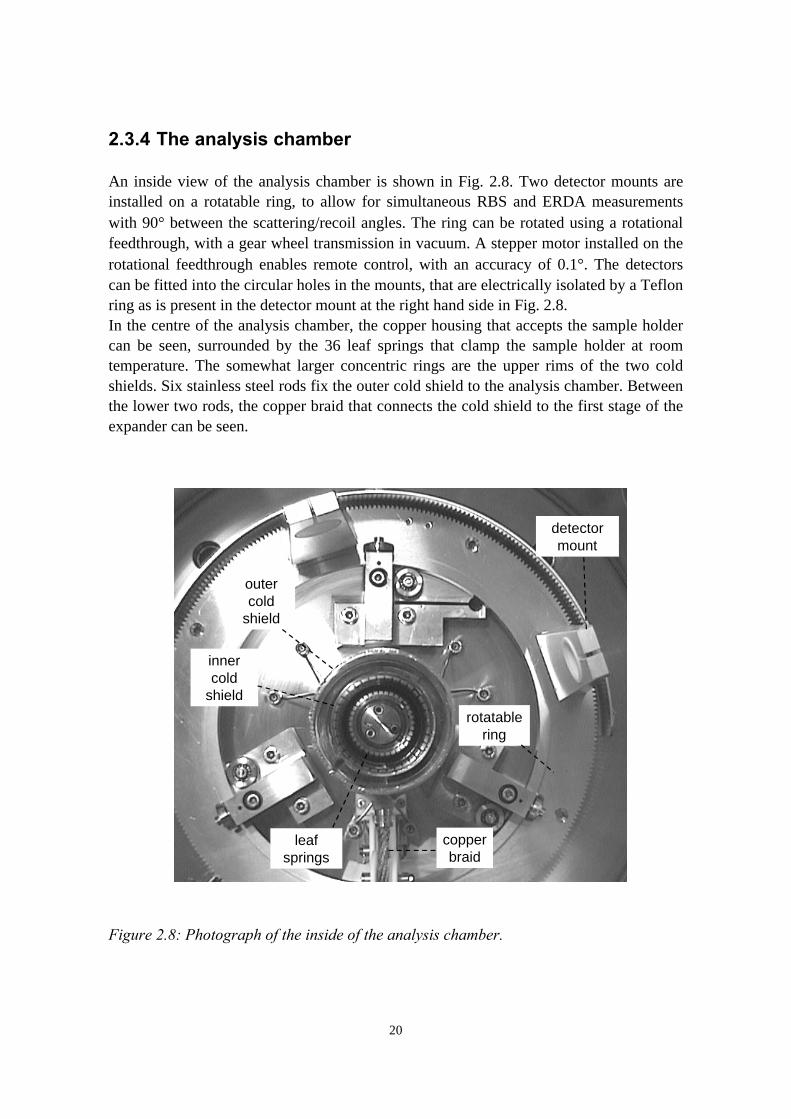
2.3.4 The analysis chamber
An inside view of the analysis chamber is shown in Fig. 2.8. Two detector mounts areinstalled on a rotatable ring, to allow for simultaneous RBS and ERDA measurementswith 90° between the scattering/recoil angles. The ring can be rotated using a rotationalfeedthrough, with a gear wheel transmission in vacuum. A stepper motor installed on therotational feedthrough enables remote control, with an accuracy of 0.1°. The detectorscan be fitted into the circular holes in the mounts, that are electrically isolated by a Teflonring as is present in the detector mount at the right hand side in Fig. 2.8.In the centre of the analysis chamber, the copper housing that accepts the sample holdercan be seen, surrounded by the 36 leaf springs that clamp the sample holder at roomtemperature. The somewhat larger concentric rings are the upper rims of the two coldshields. Six stainless steel rods fix the outer cold shield to the analysis chamber. Betweenthe lower two rods, the copper braid that connects the cold shield to the first stage of theexpander can be seen.
outercold
shield
innercold
shield
detectormount
rotatablering
copperbraid
leafsprings
Figure 2.8: Photograph of the inside of the analysis chamber.
21
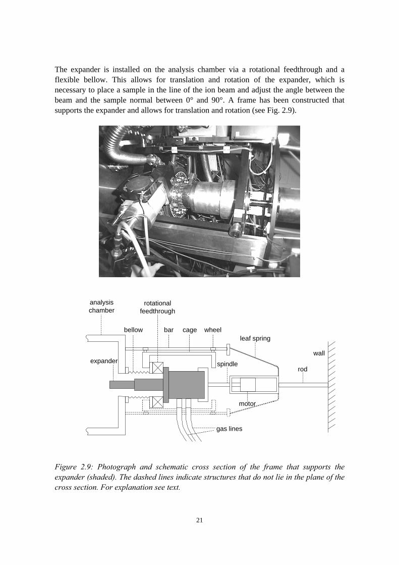
The expander is installed on the analysis chamber via a rotational feedthrough and aflexible bellow. This allows for translation and rotation of the expander, which isnecessary to place a sample in the line of the ion beam and adjust the angle between thebeam and the sample normal between 0° and 90°. A frame has been constructed thatsupports the expander and allows for translation and rotation (see Fig. 2.9).
analysischamber
cagebar wheel
rotationalfeedthrough
spindle
bellow
expander
motor
leaf spring
rod
wall
gas lines
Figure 2.9: Photograph and schematic cross section of the frame that supports theexpander (shaded). The dashed lines indicate structures that do not lie in the plane of thecross section. For explanation see text.
22
The frame consists of a steel cage resting on a number of small wheels between threesteel bars. The expander, mounted on the rotational feedthrough, is installed in the cage.The frame has been constructed such that the expander can be rotated within 90°. Therotational feedthrough is equipped with a stepper motor and gear wheel transmission, bymeans of which the angle between the sample normal and the ion beam can be adjustedwith an accuracy better than 0.1°. Translation of the cage between the bars is enabled bya spindle that is connected to the motor housing of the expander. The spindle again isdriven by a stepper motor. The translation can be adjusted with an accuracy of 0.1 mm.When the cryocooler is in operation, the expander produces considerable vibrationscaused by the moving gas displacer. When the full stroke length is used for optimalcooling capacity, the displacer will touch the walls of the expander at the end of eachstroke. Since the samples are mounted directly on the cold tip of the expander and theangle between the sample normal and the ion beam must be stable within 0.1°, thevibrations of the expander have to be controlled. We chose to give the expander fullfreedom to vibrate with respect to the analysis chamber perpendicular to the scatteringplane, while limiting torsion and wagging motions in the scattering plane as much aspossible. Therefore, no firm coupling has been applied between the analysis chamber andthe expander in the translation direction. Instead, the expander is fixed to a wall with athick steel rod via the spindle and stepper motor housing. The latter is centred withrespect to the expander frame with flexible leaf springs, which prevent the vibrationsfrom propagating to the analysis chamber. Torsion and wagging is strongly limited by theconstruction formed by the cage within the three bars.
portable vacuumcontainer
magnetictransfer rod
to analysischamber
load lock
valve
rotationstage
Figure 2.10: Schematic representation of the load lock with the portable vacuumcontainer. Two magnetic transfer rods and a rotation stage enable sample transfer fromthe vacuum container to the analysis chamber.
23
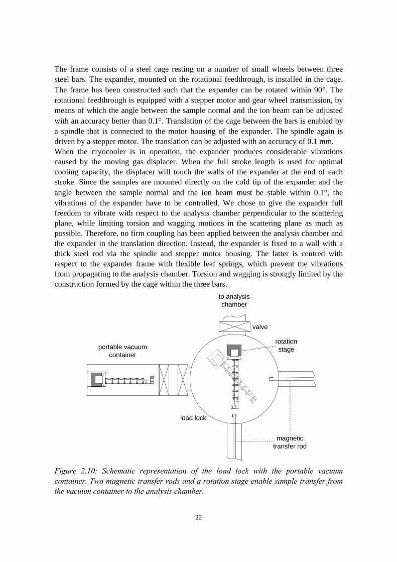
2.3.5 The load lock
The sample holder can be transferred from a portable vacuum container to the analysischamber via a load lock (see Fig. 2.10). The vacuum container can be attached to theglove box of our polymer-LED production line, which makes it possible to introducepolymer LED samples into the analysis chamber without exposure to air. A similarhousing as is present on the cold tip of the cryocooler is used to secure the sample holderinside the vacuum container. By means of a magnetic transfer rod, the sample holder canbe picked up and placed in the rotation stage in the load lock. After rotation over 90°, thesample holder can be transferred to the analysis chamber using a second magnetictransfer rod, perpendicular to the first one.
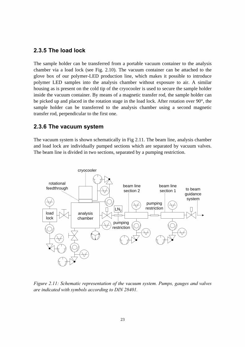
2.3.6 The vacuum system
The vacuum system is shown schematically in Fig 2.11. The beam line, analysis chamberand load lock are individually pumped sections which are separated by vacuum valves.The beam line is divided in two sections, separated by a pumping restriction.
analysischamber
loadlock
rotationalfeedthrough
cryocooler
pumpingrestriction
beam linesection 2
beam linesection 1
LN2
pumpingrestriction
to beamguidancesystem
Figure 2.11: Schematic representation of the vacuum system. Pumps, gauges and valvesare indicated with symbols according to DIN 28401.
24
Beam line section 1 consists mainly of a 5.3 m aluminium pipe with an inner diameter of45 mm. As specified in section 2.2.1, the pressure in this section must be 10-5 mbar orlower. Since the pressure in the beam guidance system is also maintained at 10-5 mbar, apumping restriction between the beam guidance system and beam line section 1 is notnecessary and the two sections can simply be connected via a pneumatic valve. The basepressure in beam line section 1 is determined by the outgassing of the walls divided bythe effective pumping speed. The outgassing coefficient of well cleaned aluminium is ofthe order of 10-9 mbar·l·s-1·cm-2 [ELS75], which means that the effective pumping speedhas to be about 1 l·s-1. The conductance C of a pipe with length L and radius r can beestimated as C = r3/L l·s-1, with r and L in mm and L>>r. The effective pumping speed Seff
in a vacuum system can be calculated from the pumping speed of the pump S and theconductance of the system C: Seff = SC/(S + C). The conductance of the aluminium pipe is2 l·s-1, therefore a small pump with a pumping speed of 50 l·s-1 is sufficient to obtain aneffective pumping speed of about 2 l·s-1. Therefore, beam line section 1 is pumped by a50 l·s-1 turbomolecular pump with a rotary vane roughing pump. The measured basepressure in the section is 5·10-6 mbar.As specified in section 2.2.1, the pressure in beam line section 2 should be 10-7 mbar orbetter. The necessary pumping speed to obtain this can be estimated by considering thegas flow through the pumping restriction between beam line sections 1 and 2 and theoutgassing of the walls. The pumping restriction consists of a stainless steel tube with aradius of 10 mm and 400 mm length, which means that the conductance is roughly 2 l·s-1.Since the pressure drop over the pumping restriction is about 10-5 mbar, a gas flow of2·10-5 mbar·l·s-1 will enter beam line section 2. The section mainly consists of a stainlesssteel tube with an inner diameter of about 100 mm and 650 mm length. The outgassingcoefficient of stainless steel is approximately 10-9 mbar·l·s-1·cm-2 [ELS75], and theoutgassing rate can therefore be approximated as 2·10-6 mbar·l·s-1 which is negligiblecompared to the gas flow originating from beam line section 1. To obtain a pressure of10-7 mbar, an effective pumping speed of 200 l·s-1 is required. Considering theconductance of the section, which is approximately 103 l·s-1, we chose a turbomolecularpump with a pumping speed of 260 l·s-1, again in combination with a rotary vaneroughing pump. The measured base pressure in beam line section 2 is 5·10-8 mbar.The most stringent vacuum demand is imposed on the analysis chamber, in which thepressure should be of the order of 10-9 mbar. The total inner area of the stainless steelchamber amounts to about 4000 cm2, which results in an outgassing rate of 4·10-6
mbar·l·s-1 using an outgassing coefficient of 10-9 mbar·l·s-1·cm-2. The gas flow through thepumping restriction is one order of magnitude lower and therefore negligible. Therequired effective pumping speed to obtain 10-9 mbar thus would be 4000 l·s-1. However,the outgassing rate of stainless steel is known to decrease considerably in time, ultimatelydown to 10-12 mbar·l·s-1·cm-2 after baking out [WOL89]. Baking out the system at hightemperature (200 °C) is not an option, since the cryocooler can only be heated to 70 °Cwithout removing most of the instrumentation and inner parts. An outgassing ratesignificantly lower than 4·10-6 mbar·l·s-1 is nevertheless to be expected if the system is
25
pumped for several weeks. Bearing the previous in mind, a 500 l·s-1 ion pump wasinstalled on the analysis chamber, as well as 250 l·s-1 turbomolecular pump incombination with a rotary vane pump as a roughing stage. With the valve between theanalysis chamber and the turbomolecular pump opened, a pressure of 5·10-8 mbar ismeasured after a few days of pumping. When the valve is subsequently closed and thesystem is pumped by only the ion pump, a pressure of 2·10-9 mbar is reached within 3-4weeks.The rotational feedthrough that connects the cryocooler to the analysis chamber containsa number of Teflon sliding seals. To reduce leakage through seals, the space between theseparate seals is pumped at two stages by a 50 l·s-1 turbomolecular pump and a rotaryvane pump.Finally, the load lock is pumped by a 50 l·s-1 turbomolecular pump in combination with arotary vane roughing pump. The measured base pressure in the load lock is 10-7 mbar.
2.3.7 Detector and sample manipulation
The rotation of the detector ring as well as the translation and rotation of the expander,i.e. the samples, are adjustable by remote control, using stepper motors and quadratureencoders. An encoder generates pulses when its shaft is rotated. By mounting an encoderon the shaft of a stepper motor, the number of revolutions can be determined by countingthe encoder pulses. Two square wave pulse trains are generated on two output channels,shifted by a quarter of a cycle. The direction of rotation can be determined from theleading channel. A so-called index signal is generated once per revolution, which can beused to initialise the system.A number of end switches have been installed in the setup, which are hit when thecorresponding moving parts approach their mechanical limits. The end switch for thedetector ring is placed inside the analysis chamber, all other end switches are positionedoutside the vacuum.A PC equipped with commercial Advantech [ADV] ISA-cards is used to control thestepper motors and read out the encoders. A program written in turbo-C allows theoperator to adjust the position of the detectors and the samples. To initialise the system,each stepper motor is moved until the corresponding end switch is hit. The motion of thestepper motor is subsequently reversed. Upon detection of the index signal generated bythe encoder, the motor stops. This procedure guaranties an accurate and reproduciblereference position.
2.4 Performance of the sample cooling system
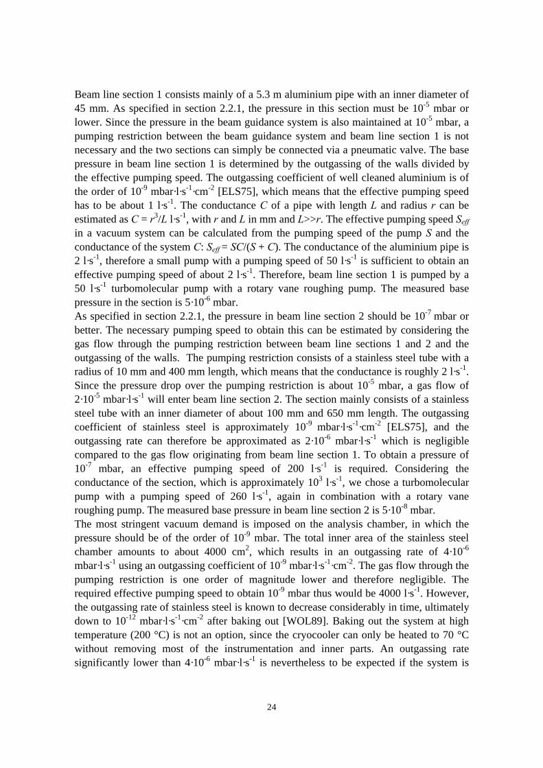
In our setup, the second expansion stage of the cryocooler reaches a temperature of 6 Kapproximately 90 minutes after start-up (see Fig. 2.12). The first expansion stageeventually reaches about 30 K, indicating that the heat load on the cold shields is indeedmuch lower than the specified cooling power of 14 W at 80 K.
26
Figure 2.12: The temperature at the two expansion stages of the cryocooler as a functionof cooling time. The second stage reaches 6 K after 90 minutes.
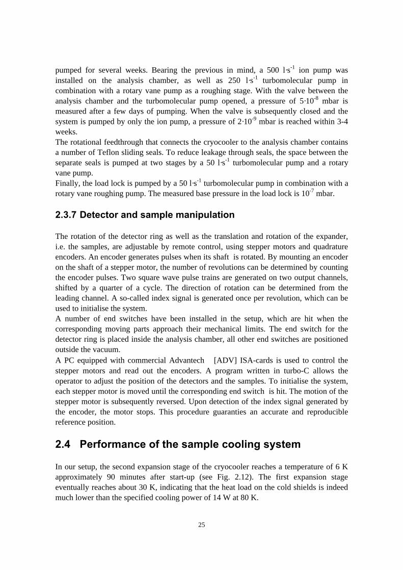
To obtain an estimate of the sample temperature during RBS/ERDA experiments onpolymer films deposited on a glass substrate, a chromel-alumel thermocouple was appliedon the surface of a glass sample, as shown in Fig. 2.13. The sample position farthest fromthe cryocooler was used. The thermocouple wires, which were 0.15 mm thick, wereclamped under one of the leaf springs that is used to press the sample on the sampleholder. The wires were bend such that the thermocouple was pressed on the samplesurface due to the tension in the wires. A small amount of thermal conductive grease wasapplied on the thermocouple and the sample to improve the thermal contact.After applying the thermocouple, the sample holder was placed in the load lock. Thethermocouple wires were connected to electrical feedthroughs which were installed onthe load lock for this purpose. A reference thermocouple in liquid nitrogen was connectedto the other end of the electrical feedthroughs, as shown in figure 2.13. The load lock wassubsequently evacuated, and the sample holder was transferred to the analysis chamberand mounted on the cold tip of the cryocooler. After cooling down to 6 K at the secondstage of the cryocooler, the temperature of the sample was measured with and withoutbeing irradiated with a 2 MeV He+ beam.The above described procedure was carried out several times, since the contact betweenthe thermocouple and the sample appeared to be very critical for the measuredtemperature. In some cases, the thermocouple read-out even changed when thecryocooler was translated, indicating a poor contact subject to changes in the tension inthe thermocouple wires. When such effects were observed, the results of themeasurements were disregarded. The accuracy of the measurements is thus limited by thecontact between the thermocouple and the sample, and the measured temperature canonly be regarded as an upper limit.
27
thermocouple
V
to analysischamber
load lock
electricalfeedthroughs
referencethermocouple
in LN2
Figure 2.13: Schematic drawing of the setup that was prepared to measure the sampletemperature during RBS/ERDA measurements. For explanation see text.
Without being irradiated by the ion beam, the sample temperature as determined by thesemeasurements lies between 20 and 30 K. With beam on target, the temperature increasesby a few degrees: about 5 degrees in case of a beam current of 10 nA and about 10degrees for a 20 nA beam. These upper limit measurements show that indeed a sampletemperature near 10 K can be reached, provided that the beam current is kept low (≈10nA). Besides the beam current, the thermal conductivity of the sample and the contactbetween the sample and the sample holder also limit the lowest achievable temperature,as will be discussed in chapter 3.The observed temperature rise of 5 K resulting from irradiation with a 10 nA 2 MeV He+
beam is in reasonable agreement with what could be expected, based on the thermalconductivity data for different types of glass reported in reference [TOU70]. The thermalconductivity λ varies roughly between 6⋅10-4 and 5⋅10-3 W⋅cm-1⋅K-1. Assuming that thebeam spot size was ≈0.1 cm2, the heat load of the ion beam was ≈0.2 W⋅cm-2. Since thesample was 1 mm thick and the impinging ions deposit their energy in the first few µmbelow the surface, the temperature gradient ∆T over the sample can be estimated as ∆T ≈0.02/λ, corresponding to ≈4 K and ≈30 K for the maximum and minimum values of λ,respectively.The measured temperature also depends on the heat conduction through the 0.15 mmthick thermocouple wires. As described above, the thermocouple wires were clamped onthe sample under one of the leaf springs. The thermocouple was located near the centre of
28
the sample surface, with ≈1 cm of wire length between the thermocouple and theclamping point. Assuming that the thermal conductivity of the thermocouple wires near10 K is of the order of 10 W⋅cm-1⋅K-1, which is an upper-limit estimate, a heat flow of≈4⋅10-3 W/K from the clamping point to the thermocouple will arise as the temperature ofthe thermocouple increases under influence of the ion beam. As a result of this, themeasured temperature increase is somewhat underestimated. Due to the long wire length(≈1 m) between the electrical feedthroughs at 293 K and the thermocouple, thecorresponding heat flow can be disregarded.
2.5 Summary and conclusions
A cryogenic RBS/ERDA setup has been constructed using a commercial Gifford-McMahon cryocooler. A shrink coupling between the cryocooler and the sample holderenables sample transfer through a load lock, while insuring a good thermal contact atcryogenic temperatures. Using a portable vacuum container, samples can be transferredfrom a remote glove box to the setup without being exposed to air. Upper limittemperature measurements have shown that a sample temperature below 30 K can bereached.
References
[ADV] Advantech (www.advantech.com), Irvine, CA 92618, USA[APD] APD cryogenics Inc. (www.apdcryogenics.com), Allentown, PA 18103-
4783, USA[BER94] B.M. van den Berg, J.A. Reinders, A.H.J. Timans, F. Labohm, M.
Breeman, P. de Groot, M. Langelaar, P.J.M. Smulders, D.O. Boerma,Nevacblad 32 (1994) 47-53
[DIJ97] P.W.L. van Dijk, A high-energy ion channelling facility and itsapplications, (PhD Dissertation, Eindhoven University of Technology,1997)
[ELS75] R.J. Elsey, Vacuum 25 (1975) 299-306, 347-361[GIF60] W.E. Gifford, H.O. McMahon, Adv. Cryogen. Engng 5 (1960) 354-367,
368-372[LAK] Lake Shore Cryotronics, Inc. (www.lakeshore.com), Westerville, OH
43081-2399, USA[SUU89] E.P.Th.M. Suurmeijer, J. Verhoeven, Vacuümtechniek, (Nederlandse
Vacuümvereniging, 1989) (in Dutch)[TOU70] Y.S. Touloukian, R.W Powell, C.Y. Ho, P.G. Klemens, Thermophysical
properties of matter, (Plenum, New York, 1970)[WAL83] G. Walker, Cryocoolers, (Plenum Press, New York, 1983)[WOL89] L. Wolterbeek Muller, Vacuümtechniek beginselen en toepassingen,
(Kluwer Technische Boeken B.V, Deventer, 1989) (in Dutch)
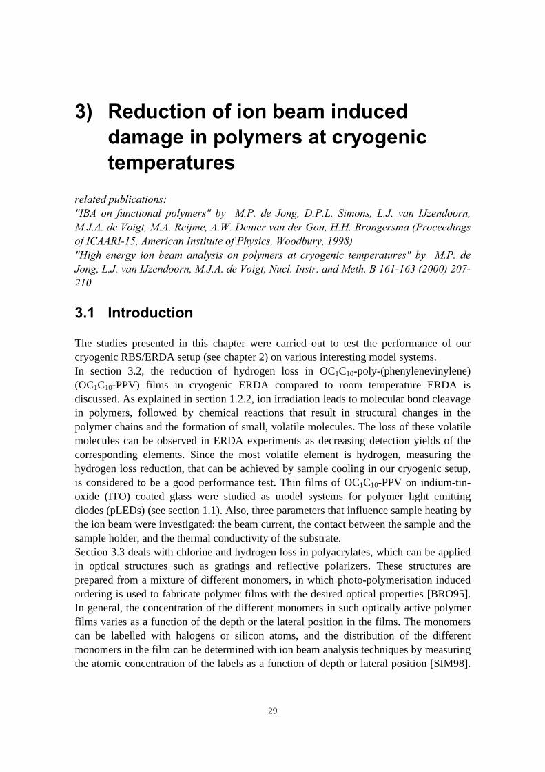
29
3) Reduction of ion beam induceddamage in polymers at cryogenictemperatures
related publications:"IBA on functional polymers" by M.P. de Jong, D.P.L. Simons, L.J. van IJzendoorn,M.J.A. de Voigt, M.A. Reijme, A.W. Denier van der Gon, H.H. Brongersma (Proceedingsof ICAARI-15, American Institute of Physics, Woodbury, 1998)"High energy ion beam analysis on polymers at cryogenic temperatures" by M.P. deJong, L.J. van IJzendoorn, M.J.A. de Voigt, Nucl. Instr. and Meth. B 161-163 (2000) 207-210
3.1 Introduction
The studies presented in this chapter were carried out to test the performance of ourcryogenic RBS/ERDA setup (see chapter 2) on various interesting model systems.In section 3.2, the reduction of hydrogen loss in OC1C10-poly-(phenylenevinylene)(OC1C10-PPV) films in cryogenic ERDA compared to room temperature ERDA isdiscussed. As explained in section 1.2.2, ion irradiation leads to molecular bond cleavagein polymers, followed by chemical reactions that result in structural changes in thepolymer chains and the formation of small, volatile molecules. The loss of these volatilemolecules can be observed in ERDA experiments as decreasing detection yields of thecorresponding elements. Since the most volatile element is hydrogen, measuring thehydrogen loss reduction, that can be achieved by sample cooling in our cryogenic setup,is considered to be a good performance test. Thin films of OC1C10-PPV on indium-tin-oxide (ITO) coated glass were studied as model systems for polymer light emittingdiodes (pLEDs) (see section 1.1). Also, three parameters that influence sample heating bythe ion beam were investigated: the beam current, the contact between the sample and thesample holder, and the thermal conductivity of the substrate.Section 3.3 deals with chlorine and hydrogen loss in polyacrylates, which can be appliedin optical structures such as gratings and reflective polarizers. These structures areprepared from a mixture of different monomers, in which photo-polymerisation inducedordering is used to fabricate polymer films with the desired optical properties [BRO95].In general, the concentration of the different monomers in such optically active polymerfilms varies as a function of the depth or the lateral position in the films. The monomerscan be labelled with halogens or silicon atoms, and the distribution of the differentmonomers in the film can be determined with ion beam analysis techniques by measuringthe atomic concentration of the labels as a function of depth or lateral position [SIM98].
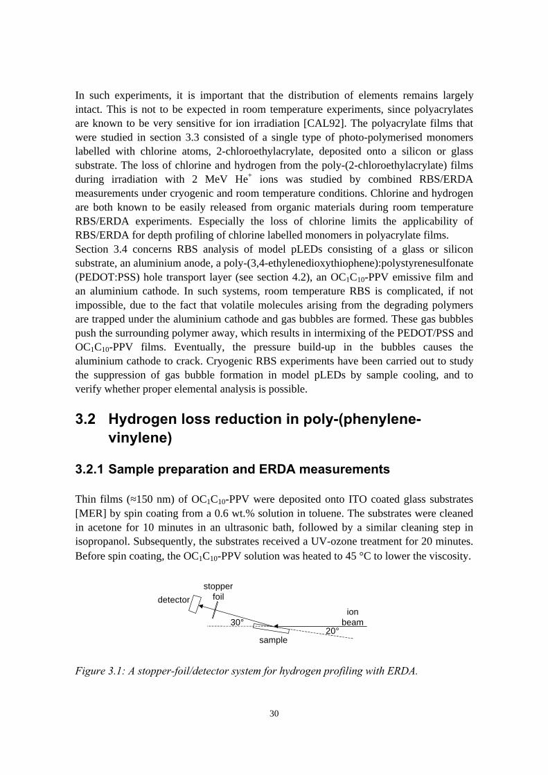
30
In such experiments, it is important that the distribution of elements remains largelyintact. This is not to be expected in room temperature experiments, since polyacrylatesare known to be very sensitive for ion irradiation [CAL92]. The polyacrylate films thatwere studied in section 3.3 consisted of a single type of photo-polymerised monomerslabelled with chlorine atoms, 2-chloroethylacrylate, deposited onto a silicon or glasssubstrate. The loss of chlorine and hydrogen from the poly-(2-chloroethylacrylate) filmsduring irradiation with 2 MeV He+ ions was studied by combined RBS/ERDAmeasurements under cryogenic and room temperature conditions. Chlorine and hydrogenare both known to be easily released from organic materials during room temperatureRBS/ERDA experiments. Especially the loss of chlorine limits the applicability ofRBS/ERDA for depth profiling of chlorine labelled monomers in polyacrylate films.Section 3.4 concerns RBS analysis of model pLEDs consisting of a glass or siliconsubstrate, an aluminium anode, a poly-(3,4-ethylenedioxythiophene):polystyrenesulfonate(PEDOT:PSS) hole transport layer (see section 4.2), an OC1C10-PPV emissive film andan aluminium cathode. In such systems, room temperature RBS is complicated, if notimpossible, due to the fact that volatile molecules arising from the degrading polymersare trapped under the aluminium cathode and gas bubbles are formed. These gas bubblespush the surrounding polymer away, which results in intermixing of the PEDOT/PSS andOC1C10-PPV films. Eventually, the pressure build-up in the bubbles causes thealuminium cathode to crack. Cryogenic RBS experiments have been carried out to studythe suppression of gas bubble formation in model pLEDs by sample cooling, and toverify whether proper elemental analysis is possible.
3.2 Hydrogen loss reduction in poly-(phenylene-vinylene)
3.2.1 Sample preparation and ERDA measurements
Thin films (≈150 nm) of OC1C10-PPV were deposited onto ITO coated glass substrates[MER] by spin coating from a 0.6 wt.% solution in toluene. The substrates were cleanedin acetone for 10 minutes in an ultrasonic bath, followed by a similar cleaning step inisopropanol. Subsequently, the substrates received a UV-ozone treatment for 20 minutes.Before spin coating, the OC1C10-PPV solution was heated to 45 °C to lower the viscosity.
sample
30°20°
ionbeam
detector
stopperfoil
Figure 3.1: A stopper-foil/detector system for hydrogen profiling with ERDA.
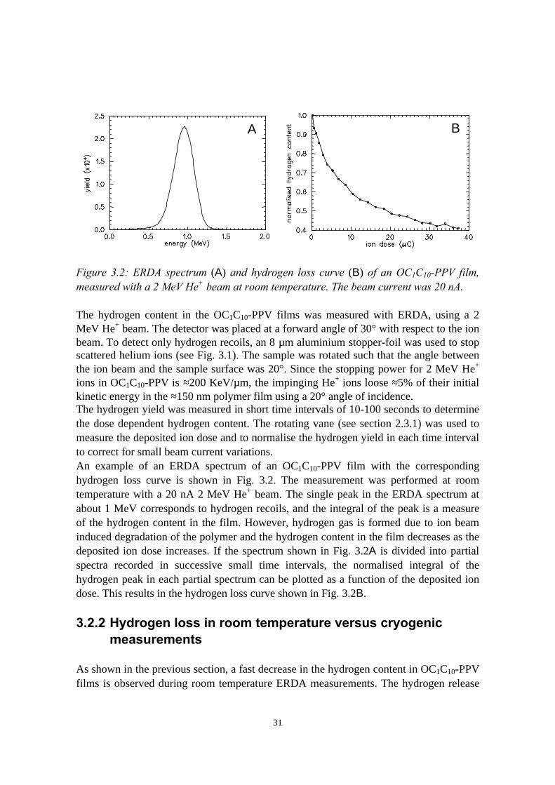
31
A B
Figure 3.2: ERDA spectrum (A) and hydrogen loss curve (B) of an OC1C10-PPV film,measured with a 2 MeV He+ beam at room temperature. The beam current was 20 nA.
The hydrogen content in the OC1C10-PPV films was measured with ERDA, using a 2MeV He+ beam. The detector was placed at a forward angle of 30° with respect to the ionbeam. To detect only hydrogen recoils, an 8 µm aluminium stopper-foil was used to stopscattered helium ions (see Fig. 3.1). The sample was rotated such that the angle betweenthe ion beam and the sample surface was 20°. Since the stopping power for 2 MeV He+
ions in OC1C10-PPV is ≈200 KeV/µm, the impinging He+ ions loose ≈5% of their initialkinetic energy in the ≈150 nm polymer film using a 20° angle of incidence. The hydrogen yield was measured in short time intervals of 10-100 seconds to determinethe dose dependent hydrogen content. The rotating vane (see section 2.3.1) was used tomeasure the deposited ion dose and to normalise the hydrogen yield in each time intervalto correct for small beam current variations.An example of an ERDA spectrum of an OC1C10-PPV film with the correspondinghydrogen loss curve is shown in Fig. 3.2. The measurement was performed at roomtemperature with a 20 nA 2 MeV He+ beam. The single peak in the ERDA spectrum atabout 1 MeV corresponds to hydrogen recoils, and the integral of the peak is a measureof the hydrogen content in the film. However, hydrogen gas is formed due to ion beaminduced degradation of the polymer and the hydrogen content in the film decreases as thedeposited ion dose increases. If the spectrum shown in Fig. 3.2A is divided into partialspectra recorded in successive small time intervals, the normalised integral of thehydrogen peak in each partial spectrum can be plotted as a function of the deposited iondose. This results in the hydrogen loss curve shown in Fig. 3.2B.
3.2.2 Hydrogen loss in room temperature versus cryogenicmeasurements
As shown in the previous section, a fast decrease in the hydrogen content in OC1C10-PPVfilms is observed during room temperature ERDA measurements. The hydrogen release
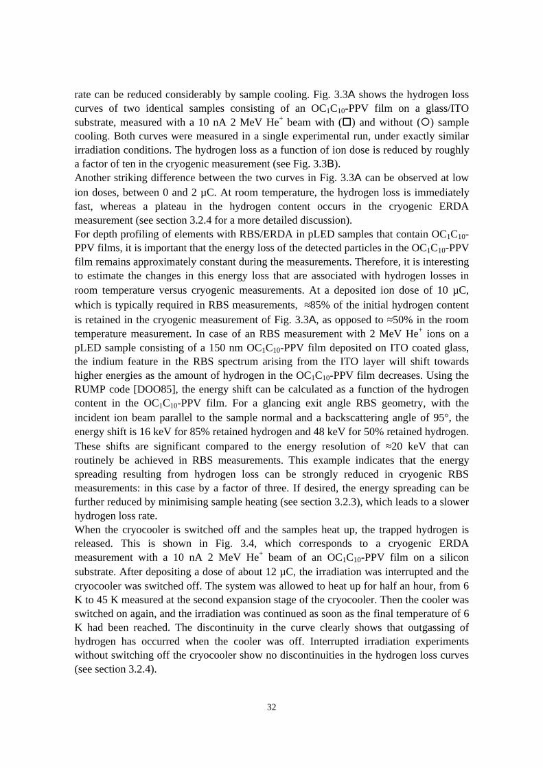
32
rate can be reduced considerably by sample cooling. Fig. 3.3A shows the hydrogen losscurves of two identical samples consisting of an OC1C10-PPV film on a glass/ITOsubstrate, measured with a 10 nA 2 MeV He+ beam with (o) and without (¡) samplecooling. Both curves were measured in a single experimental run, under exactly similarirradiation conditions. The hydrogen loss as a function of ion dose is reduced by roughlya factor of ten in the cryogenic measurement (see Fig. 3.3B).Another striking difference between the two curves in Fig. 3.3A can be observed at lowion doses, between 0 and 2 µC. At room temperature, the hydrogen loss is immediatelyfast, whereas a plateau in the hydrogen content occurs in the cryogenic ERDAmeasurement (see section 3.2.4 for a more detailed discussion).For depth profiling of elements with RBS/ERDA in pLED samples that contain OC1C10-PPV films, it is important that the energy loss of the detected particles in the OC1C10-PPVfilm remains approximately constant during the measurements. Therefore, it is interestingto estimate the changes in this energy loss that are associated with hydrogen losses inroom temperature versus cryogenic measurements. At a deposited ion dose of 10 µC,which is typically required in RBS measurements, ≈85% of the initial hydrogen contentis retained in the cryogenic measurement of Fig. 3.3A, as opposed to ≈50% in the roomtemperature measurement. In case of an RBS measurement with 2 MeV He+ ions on apLED sample consisting of a 150 nm OC1C10-PPV film deposited on ITO coated glass,the indium feature in the RBS spectrum arising from the ITO layer will shift towardshigher energies as the amount of hydrogen in the OC1C10-PPV film decreases. Using theRUMP code [DOO85], the energy shift can be calculated as a function of the hydrogencontent in the OC1C10-PPV film. For a glancing exit angle RBS geometry, with theincident ion beam parallel to the sample normal and a backscattering angle of 95°, theenergy shift is 16 keV for 85% retained hydrogen and 48 keV for 50% retained hydrogen.These shifts are significant compared to the energy resolution of ≈20 keV that canroutinely be achieved in RBS measurements. This example indicates that the energyspreading resulting from hydrogen loss can be strongly reduced in cryogenic RBSmeasurements: in this case by a factor of three. If desired, the energy spreading can befurther reduced by minimising sample heating (see section 3.2.3), which leads to a slowerhydrogen loss rate.When the cryocooler is switched off and the samples heat up, the trapped hydrogen isreleased. This is shown in Fig. 3.4, which corresponds to a cryogenic ERDAmeasurement with a 10 nA 2 MeV He+ beam of an OC1C10-PPV film on a siliconsubstrate. After depositing a dose of about 12 µC, the irradiation was interrupted and thecryocooler was switched off. The system was allowed to heat up for half an hour, from 6K to 45 K measured at the second expansion stage of the cryocooler. Then the cooler wasswitched on again, and the irradiation was continued as soon as the final temperature of 6K had been reached. The discontinuity in the curve clearly shows that outgassing ofhydrogen has occurred when the cooler was off. Interrupted irradiation experimentswithout switching off the cryocooler show no discontinuities in the hydrogen loss curves(see section 3.2.4).
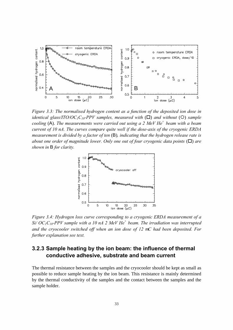
33
BA
Figure 3.3: The normalised hydrogen content as a function of the deposited ion dose inidentical glass/ITO/OC1C10-PPV samples, measured with (o) and without (¡) samplecooling (A). The measurements were carried out using a 2 MeV He+ beam with a beamcurrent of 10 nA. The curves compare quite well if the dose-axis of the cryogenic ERDAmeasurement is divided by a factor of ten (B), indicating that the hydrogen release rate isabout one order of magnitude lower. Only one out of four cryogenic data points (o) areshown in B for clarity.
Figure 3.4: Hydrogen loss curve corresponding to a cryogenic ERDA measurement of aSi/ OC1C10-PPV sample with a 10 nA 2 MeV He+ beam. The irradiation was interruptedand the cryocooler switched off when an ion dose of 12 µC had been deposited. Forfurther explanation see text.
3.2.3 Sample heating by the ion beam: the influence of thermalconductive adhesive, substrate and beam current
The thermal resistance between the samples and the cryocooler should be kept as small aspossible to reduce sample heating by the ion beam. This resistance is mainly determinedby the thermal conductivity of the samples and the contact between the samples and thesample holder.
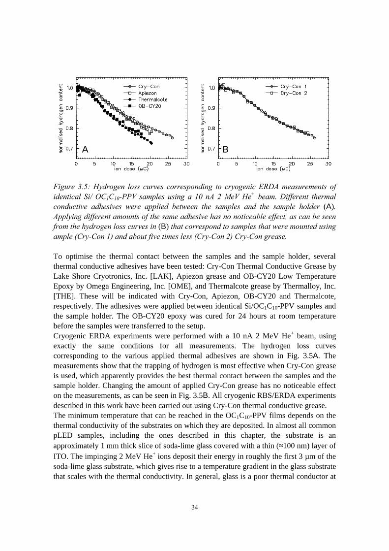
34
BA
Figure 3.5: Hydrogen loss curves corresponding to cryogenic ERDA measurements ofidentical Si/ OC1C10-PPV samples using a 10 nA 2 MeV He+ beam. Different thermalconductive adhesives were applied between the samples and the sample holder (A).Applying different amounts of the same adhesive has no noticeable effect, as can be seenfrom the hydrogen loss curves in (B) that correspond to samples that were mounted usingample (Cry-Con 1) and about five times less (Cry-Con 2) Cry-Con grease.
To optimise the thermal contact between the samples and the sample holder, severalthermal conductive adhesives have been tested: Cry-Con Thermal Conductive Grease byLake Shore Cryotronics, Inc. [LAK], Apiezon grease and OB-CY20 Low TemperatureEpoxy by Omega Engineering, Inc. [OME], and Thermalcote grease by Thermalloy, Inc.[THE]. These will be indicated with Cry-Con, Apiezon, OB-CY20 and Thermalcote,respectively. The adhesives were applied between identical Si/OC1C10-PPV samples andthe sample holder. The OB-CY20 epoxy was cured for 24 hours at room temperaturebefore the samples were transferred to the setup.Cryogenic ERDA experiments were performed with a 10 nA 2 MeV He+ beam, usingexactly the same conditions for all measurements. The hydrogen loss curvescorresponding to the various applied thermal adhesives are shown in Fig. 3.5A. Themeasurements show that the trapping of hydrogen is most effective when Cry-Con greaseis used, which apparently provides the best thermal contact between the samples and thesample holder. Changing the amount of applied Cry-Con grease has no noticeable effecton the measurements, as can be seen in Fig. 3.5B. All cryogenic RBS/ERDA experimentsdescribed in this work have been carried out using Cry-Con thermal conductive grease.The minimum temperature that can be reached in the OC1C10-PPV films depends on thethermal conductivity of the substrates on which they are deposited. In almost all commonpLED samples, including the ones described in this chapter, the substrate is anapproximately 1 mm thick slice of soda-lime glass covered with a thin (≈100 nm) layer ofITO. The impinging 2 MeV He+ ions deposit their energy in roughly the first 3 µm of thesoda-lime glass substrate, which gives rise to a temperature gradient in the glass substratethat scales with the thermal conductivity. In general, glass is a poor thermal conductor at
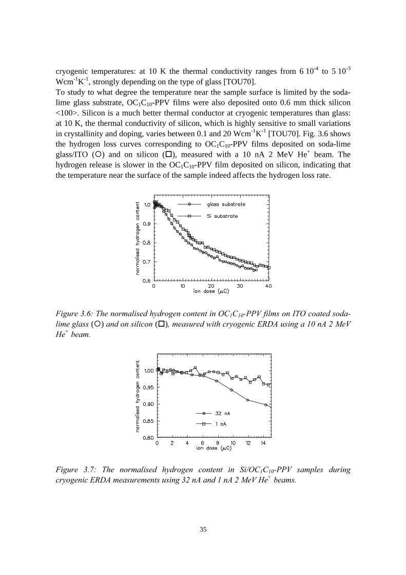
35
cryogenic temperatures: at 10 K the thermal conductivity ranges from 6⋅10-4 to 5⋅10-3
Wcm-1K-1, strongly depending on the type of glass [TOU70].To study to what degree the temperature near the sample surface is limited by the soda-lime glass substrate, OC1C10-PPV films were also deposited onto 0.6 mm thick silicon<100>. Silicon is a much better thermal conductor at cryogenic temperatures than glass:at 10 K, the thermal conductivity of silicon, which is highly sensitive to small variationsin crystallinity and doping, varies between 0.1 and 20 Wcm-1K-1 [TOU70]. Fig. 3.6 showsthe hydrogen loss curves corresponding to OC1C10-PPV films deposited on soda-limeglass/ITO (¡) and on silicon (o), measured with a 10 nA 2 MeV He+ beam. Thehydrogen release is slower in the OC1C10-PPV film deposited on silicon, indicating thatthe temperature near the surface of the sample indeed affects the hydrogen loss rate.
Figure 3.6: The normalised hydrogen content in OC1C10-PPV films on ITO coated soda-lime glass (¡) and on silicon (o), measured with cryogenic ERDA using a 10 nA 2 MeVHe+ beam.
Figure 3.7: The normalised hydrogen content in Si/OC1C10-PPV samples duringcryogenic ERDA measurements using 32 nA and 1 nA 2 MeV He+ beams.
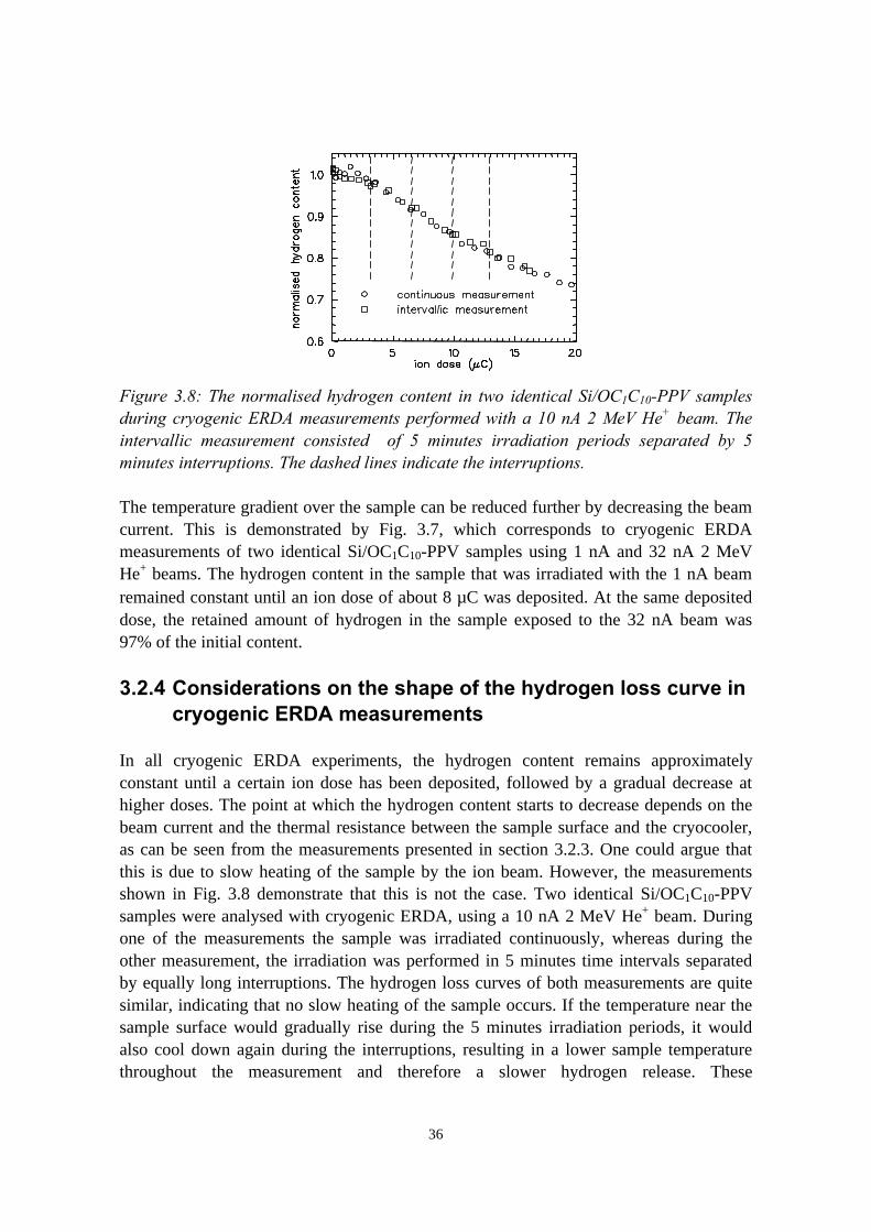
36
Figure 3.8: The normalised hydrogen content in two identical Si/OC1C10-PPV samplesduring cryogenic ERDA measurements performed with a 10 nA 2 MeV He+ beam. Theintervallic measurement consisted of 5 minutes irradiation periods separated by 5minutes interruptions. The dashed lines indicate the interruptions.
The temperature gradient over the sample can be reduced further by decreasing the beamcurrent. This is demonstrated by Fig. 3.7, which corresponds to cryogenic ERDAmeasurements of two identical Si/OC1C10-PPV samples using 1 nA and 32 nA 2 MeVHe+ beams. The hydrogen content in the sample that was irradiated with the 1 nA beamremained constant until an ion dose of about 8 µC was deposited. At the same depositeddose, the retained amount of hydrogen in the sample exposed to the 32 nA beam was97% of the initial content.
3.2.4 Considerations on the shape of the hydrogen loss curve incryogenic ERDA measurements
In all cryogenic ERDA experiments, the hydrogen content remains approximatelyconstant until a certain ion dose has been deposited, followed by a gradual decrease athigher doses. The point at which the hydrogen content starts to decrease depends on thebeam current and the thermal resistance between the sample surface and the cryocooler,as can be seen from the measurements presented in section 3.2.3. One could argue thatthis is due to slow heating of the sample by the ion beam. However, the measurementsshown in Fig. 3.8 demonstrate that this is not the case. Two identical Si/OC1C10-PPVsamples were analysed with cryogenic ERDA, using a 10 nA 2 MeV He+ beam. Duringone of the measurements the sample was irradiated continuously, whereas during theother measurement, the irradiation was performed in 5 minutes time intervals separatedby equally long interruptions. The hydrogen loss curves of both measurements are quitesimilar, indicating that no slow heating of the sample occurs. If the temperature near thesample surface would gradually rise during the 5 minutes irradiation periods, it wouldalso cool down again during the interruptions, resulting in a lower sample temperaturethroughout the measurement and therefore a slower hydrogen release. These
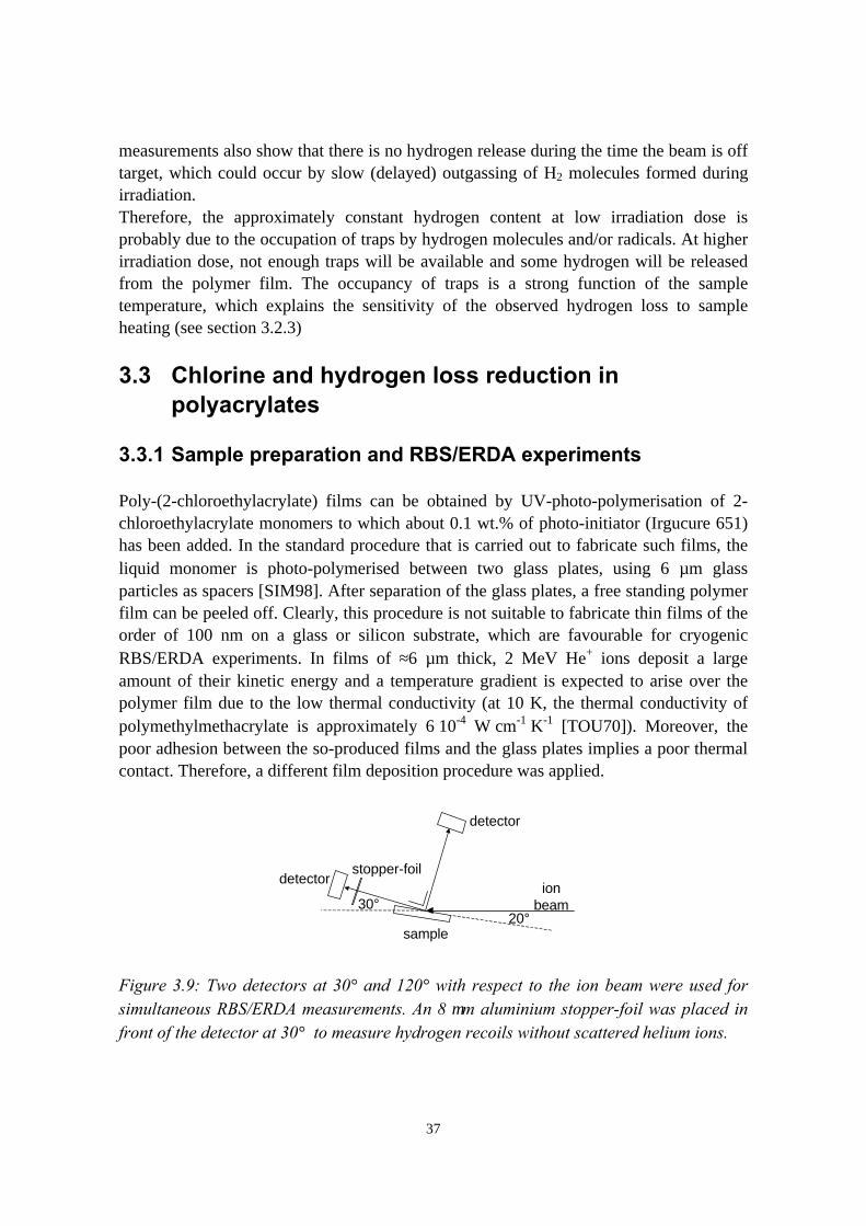
37
measurements also show that there is no hydrogen release during the time the beam is offtarget, which could occur by slow (delayed) outgassing of H2 molecules formed duringirradiation.Therefore, the approximately constant hydrogen content at low irradiation dose isprobably due to the occupation of traps by hydrogen molecules and/or radicals. At higherirradiation dose, not enough traps will be available and some hydrogen will be releasedfrom the polymer film. The occupancy of traps is a strong function of the sampletemperature, which explains the sensitivity of the observed hydrogen loss to sampleheating (see section 3.2.3)
3.3 Chlorine and hydrogen loss reduction inpolyacrylates
3.3.1 Sample preparation and RBS/ERDA experiments
Poly-(2-chloroethylacrylate) films can be obtained by UV-photo-polymerisation of 2-chloroethylacrylate monomers to which about 0.1 wt.% of photo-initiator (Irgucure 651)has been added. In the standard procedure that is carried out to fabricate such films, theliquid monomer is photo-polymerised between two glass plates, using 6 µm glassparticles as spacers [SIM98]. After separation of the glass plates, a free standing polymerfilm can be peeled off. Clearly, this procedure is not suitable to fabricate thin films of theorder of 100 nm on a glass or silicon substrate, which are favourable for cryogenicRBS/ERDA experiments. In films of ≈6 µm thick, 2 MeV He+ ions deposit a largeamount of their kinetic energy and a temperature gradient is expected to arise over thepolymer film due to the low thermal conductivity (at 10 K, the thermal conductivity ofpolymethylmethacrylate is approximately 6⋅10-4 W⋅cm-1⋅K-1 [TOU70]). Moreover, thepoor adhesion between the so-produced films and the glass plates implies a poor thermalcontact. Therefore, a different film deposition procedure was applied.
sample
30°20°
ionbeam
detectorstopper-foil
detector
Figure 3.9: Two detectors at 30° and 120° with respect to the ion beam were used forsimultaneous RBS/ERDA measurements. An 8 µm aluminium stopper-foil was placed infront of the detector at 30° to measure hydrogen recoils without scattered helium ions.
38
A mixture of 1.466 g 2-chloroethylacrylate and 4.6⋅10-3 g photo-initiator was illuminatedin a closed jar with UV-light from a Philips PLS-9W/10 Black Light (350-390 nm, 2.2W). The illumination was stopped as soon as the formation of a solid polymer wasobserved. The remaining liquid fraction consisted of poly-(2-chloroethylacrylate) solvedin its monomer, and films of approximately 200 nm could be obtained by spin coatingthe liquid onto silicon substrates. Prior to spin coating, the silicon substrates were cleanedin ultrasonic baths of acetone and isopropanol for 10 minutes each, followed by a 20minutes UV-ozone treatment.Simultaneous RBS and ERDA measurements were performed with two detectors, placedat 30° and 120° with respect to the impinging 2 MeV He+ beam (see Fig. 3.9). An 8 µmaluminium stopper-foil was placed in front of the ERDA detector to stop scattered heliumions and measure only hydrogen recoils. The chlorine content in the films wasdetermined from the RBS measurements. A similar procedure as described in section3.2.1 was carried out to measure hydrogen and chlorine losses as a function of thedeposited ion dose.
3.3.2 Chlorine and hydrogen loss in room temperature versuscryogenic measurements
Fig. 3.10 shows the normalised hydrogen and chlorine content in two identical Si/poly-(2-chloroethylacrylate) samples as a function of the deposited ion dose, measured withroom temperature RBS/ERDA and cryogenic RBS/ERDA, respectively. Themeasurements were performed with a 20 nA 2 MeV He+ beam. During the roomtemperature measurement, fast depletion of both hydrogen and chlorine was observed. Asa consequence of the extremely rapid loss of chlorine, depth profiling of chlorine labelledmonomers in polyacrylate films is nearly impossible with room temperature RBS. Thefast decrease of the chlorine content is most probably due to the fact that chlorineeffectively traps low energy secondary electrons, which are produced along the tracks ofthe impinging ions. The formed temporary negative ions will dissociate and form Cl- andan organic radical. The high electron affinity of Cl is the driving force for this reaction.The reactive Cl- ions can easily form volatile chlorine compounds (Cl2, HCl, etc.).In the cryogenic measurement, the loss of H and Cl is considerably reduced: at 10 µCdeposited ion dose, the hydrogen loss is reduced from 50% to 10% and the chlorine lossfrom more than 90% to about 5%. In spite of the fact that chlorine is released much fasterthan hydrogen at room temperature, the trapping of chlorine compounds like HCl and Cl2
in the film during the cryogenic measurement is more effective than the trapping of H2: attemperatures near 10 K, the vapour pressures of HCl and Cl2 are almost zero, whereas thevapour pressure of H2 is still a few mbar [HAN74]. It can be concluded that, thanks to thealmost complete suppression of chlorine loss, depth profiling of chlorine labelledmonomers in polyacrylate films has become possible with cryogenic RBS.

39
A B
Figure 3.10: The normalised hydrogen (A) and chlorine (B) content in Si/poly-(2-chloroethylacrylate) samples as a function of ion dose in room temperature (¡) andcryogenic (o) RBS/ERDA measurements with a 20 nA 2 MeV He+ beam.
3.4 Damage reduction in model polymer light emittingdiodes with encapsulated polymer films
3.4.1 Sample preparation and RBS experiments
The model pLEDs were prepared at Philips Research Laboratories according to thefollowing procedure. Silicon or glass substrates were cleaned with several detergents,followed by a UV-ozone treatment for 15 minutes. An aluminium anode wassubsequently deposited onto the substrates by evaporation in vacuum. On top of thealuminium anode, a poly-(3,4-ethylenedioxythiophene):poly-styrenesulfonate (PEDOT:PSS) hole transport layer (see also section 4.2 and chapter 7) was deposited by spincoating from an aqueous suspension under ambient conditions. The samples were driedby annealing at 150 °C for 5 minutes and transferred to a glove box with a nitrogenatmosphere, followed by a similar annealing treatment. Subsequently, an OC1C10-PPVemissive film was deposited in the glove box by spin coating from a 1 wt.% solution intoluene. Directly afterwards, the samples were transferred to a built-in evaporationchamber where an aluminium cathode was deposited.RBS experiments were carried out with 2 MeV He+ beams, using a backscattering angleof 170° for optimal mass separation. To study whether the PEDOT:PSS/PPV interfaceremained sharp during the ion bombardment, the RBS spectra again were recorded insuccessive small time intervals (10-100 s).
40
3.4.2 Damage in room temperature versus cryogenic RBSexperiments
Fig. 3.11A shows a room temperature RBS spectrum of a model pLED, consisting of aPEDOT:PSS film (6 at.% S, 43 at.% C, 35 at.% H, 17 at.% O) and an OC1C10-PPV film(39 at.% C, 57 at.% H, 4 at.% O), each about 200 nm thick, between two 70 nmaluminium electrodes on a silicon substrate. Simulations of the RBS measurements wereperformed with the RUMP code [DOO85], using the above given composition forPEDOT:PSS and OC1C10-PPV. The discrepancy between the simulations and themeasurements at low energy arises from multiple scattering of helium ions, which is nottaken into account in the RUMP code. Considering the known layer stack, the sulphurfeature would be expected to lie between 1 and 1.1 MeV corresponding to sulphur in thePEDOT:PSS film. The measured sulphur step between 1.1 and 1.2 MeV, shown fivetimes enlarged in Fig. 3.11A, corresponds to a sulphur location in the OC1C10-PPV filmand moreover increases with the deposited ion dose (see Fig. 3.11B). The appearance ofthis sulphur step in the RBS spectrum must therefore be due to ion beam induceddegradation.A possible explanation for the detection of sulphur in the OC1C10-PPV film of a damagedpLED could be given by assuming that mobile sulphur compounds are formed in thePEDOT:PSS layer, which subsequently engage in chemical reactions in the overlyingOC1C10-PPV film. However, no sulphur has been detected in the OC1C10-PPV films ofsimilar samples that lacked the aluminium top layer (see Fig. 3.12), which means that theencapsulation of the polymer films by the aluminium cathode plays a crucial role.Due to the presence of the aluminium cathode, the volatile molecules that are formed inthe polymer films under ion irradiation cannot escape from the sample and gas bubblesare formed. These gas bubbles leave blisters on the sample surface, which can easily bespotted with the naked eye. Fig. 3.13A shows a photograph of three of such blisters, takenwith a CCD-camera installed on an optical microscope. Due to the build-up of pressure inthe gas bubbles, the aluminium film is stretched until it finally cracks (see Fig. 3.13B).As the gas bubbles expand, the surrounding polymer is pushed away and the PEDOT:PSSand OC1C10-PPV films will become intermixed. This would result in the detection ofsulphur directly under the aluminium cathode, as is the case in the RBS spectrum shownin Fig. 3.11A.Gas bubble formation in encapsulated polymer films is a major limitation for theapplicability of room temperature RBS/ERDA on structures as pLEDs. Even the depthdistribution of non-volatile elements, such as sulphur in the above described case, iscompletely disturbed. This means that accurate depth profiling is not possible, especiallyif the concentration of the elements to be profiled is low and a high ion dose is required.
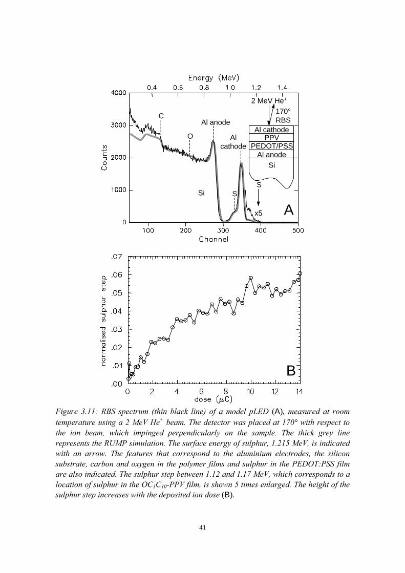
41
Si
PEDOT/PSSAl anode
PPVAl cathode
2 MeV He+
170°RBSAl anode
Alcathode
Si SS
O
C
x5 A
B
Figure 3.11: RBS spectrum (thin black line) of a model pLED (A), measured at roomtemperature using a 2 MeV He+ beam. The detector was placed at 170° with respect tothe ion beam, which impinged perpendicularly on the sample. The thick grey linerepresents the RUMP simulation. The surface energy of sulphur, 1.215 MeV, is indicatedwith an arrow. The features that correspond to the aluminium electrodes, the siliconsubstrate, carbon and oxygen in the polymer films and sulphur in the PEDOT:PSS filmare also indicated. The sulphur step between 1.12 and 1.17 MeV, which corresponds to alocation of sulphur in the OC1C10-PPV film, is shown 5 times enlarged. The height of thesulphur step increases with the deposited ion dose (B).
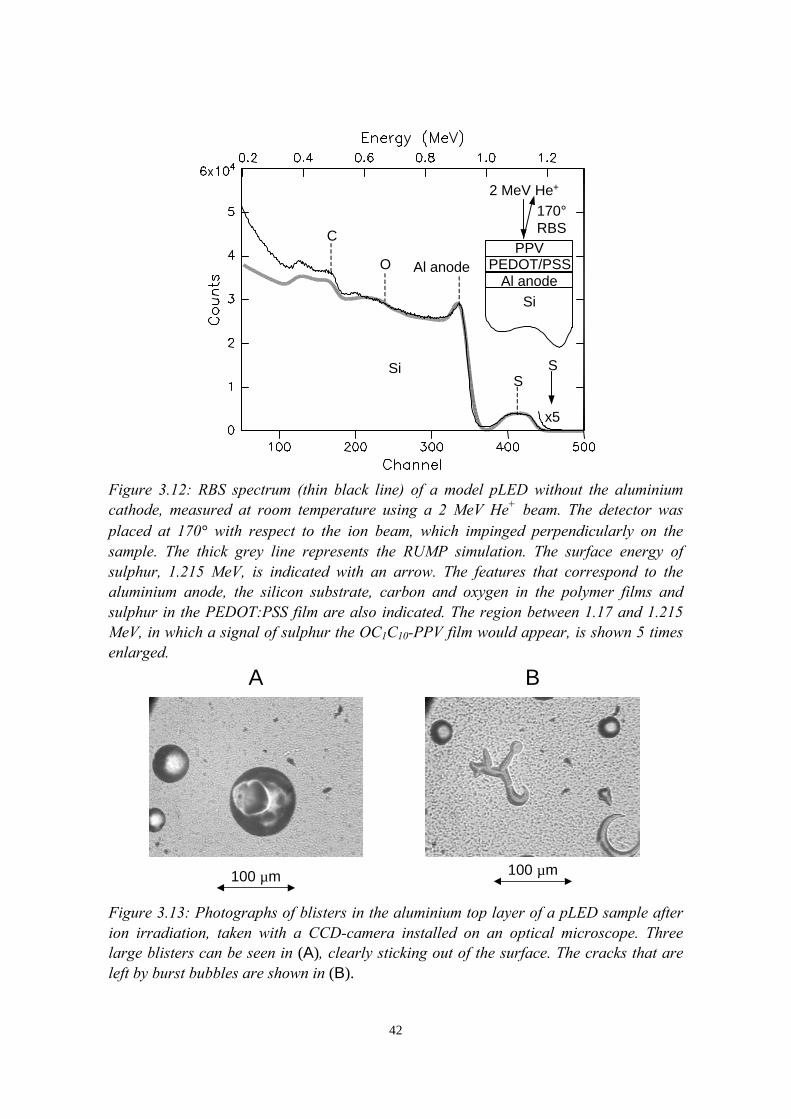
42
Al anode
SiS
S
O
C
x5
Si
PEDOT/PSSAl anode
PPV
2 MeV He+
170°RBS
Figure 3.12: RBS spectrum (thin black line) of a model pLED without the aluminiumcathode, measured at room temperature using a 2 MeV He+ beam. The detector wasplaced at 170° with respect to the ion beam, which impinged perpendicularly on thesample. The thick grey line represents the RUMP simulation. The surface energy ofsulphur, 1.215 MeV, is indicated with an arrow. The features that correspond to thealuminium anode, the silicon substrate, carbon and oxygen in the polymer films andsulphur in the PEDOT:PSS film are also indicated. The region between 1.17 and 1.215MeV, in which a signal of sulphur the OC1C10-PPV film would appear, is shown 5 timesenlarged.
100 µm
A B
100 µm
Figure 3.13: Photographs of blisters in the aluminium top layer of a pLED sample afterion irradiation, taken with a CCD-camera installed on an optical microscope. Threelarge blisters can be seen in (A), clearly sticking out of the surface. The cracks that areleft by burst bubbles are shown in (B).
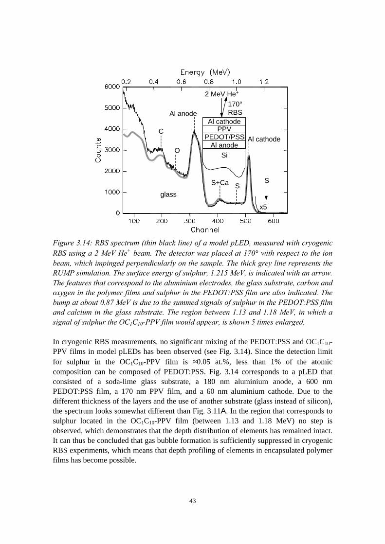
43
Al anode
Al cathode
glassS
S
O
C
x5
S+Ca
Si
PEDOT/PSSAl anode
PPVAl cathode
2 MeV He+
170°RBS
Figure 3.14: RBS spectrum (thin black line) of a model pLED, measured with cryogenicRBS using a 2 MeV He+ beam. The detector was placed at 170° with respect to the ionbeam, which impinged perpendicularly on the sample. The thick grey line represents theRUMP simulation. The surface energy of sulphur, 1.215 MeV, is indicated with an arrow.The features that correspond to the aluminium electrodes, the glass substrate, carbon andoxygen in the polymer films and sulphur in the PEDOT:PSS film are also indicated. Thebump at about 0.87 MeV is due to the summed signals of sulphur in the PEDOT:PSS filmand calcium in the glass substrate. The region between 1.13 and 1.18 MeV, in which asignal of sulphur the OC1C10-PPV film would appear, is shown 5 times enlarged.
In cryogenic RBS measurements, no significant mixing of the PEDOT:PSS and OC1C10-PPV films in model pLEDs has been observed (see Fig. 3.14). Since the detection limitfor sulphur in the OC1C10-PPV film is ≈0.05 at.%, less than 1% of the atomiccomposition can be composed of PEDOT:PSS. Fig. 3.14 corresponds to a pLED thatconsisted of a soda-lime glass substrate, a 180 nm aluminium anode, a 600 nmPEDOT:PSS film, a 170 nm PPV film, and a 60 nm aluminium cathode. Due to thedifferent thickness of the layers and the use of another substrate (glass instead of silicon),the spectrum looks somewhat different than Fig. 3.11A. In the region that corresponds tosulphur located in the OC1C10-PPV film (between 1.13 and 1.18 MeV) no step isobserved, which demonstrates that the depth distribution of elements has remained intact.It can thus be concluded that gas bubble formation is sufficiently suppressed in cryogenicRBS experiments, which means that depth profiling of elements in encapsulated polymerfilms has become possible.
44
No blisters could be observed with the naked eye on irradiated samples which still weremounted on the cryocooler. Inspection of a sample under a microscope was of courseonly possible after it had heated up again, and similar blisters and cracks were observedas shown in Fig. 3.13.
3.5 Conclusions
The hydrogen loss rate in OC1C10-PPV films on ITO coated glass is reduced by a factorof ten in cryogenic ERDA compared to room temperature ERDA, using a 10 nA 2 MeVHe+ beam. Further reduction of the hydrogen loss rate is possible by decreasing thetemperature gradient over the sample. This can be done by selecting a substrate with ahigher thermal conductivity, such as silicon, and/or by lowering the beam current.Reducing the hydrogen loss in cryogenic measurements also leads to a decrease of thecorresponding energy spreading of the detected particles in RBS/ERDA experiments. Fortypical glancing angle RBS experiments with a 10 nA 2 MeV He+ beam onglass/ITO/OC1C10-PPV samples, the energy spreading resulting from hydrogen loss canbe reduced by roughly a factor of three in cryogenic measurements as compared to roomtemperature measurements.During cryogenic ERDA measurements, the hydrogen content remains approximatelyconstant until a certain ion dose has been deposited. This is probably due to theoccupation of traps in the cold polymer by hydrogen radicals and/or molecules. As thedeposited ion dose increases, less traps will be available and some hydrogen will bereleased.Chlorine loss in poly-(2-chloroethylacrylate) films on silicon is almost completelysuppressed in cryogenic RBS measurements. Due to the relatively low vapour pressuresof chlorine compounds like HCl and Cl2, chlorine is more effectively trapped thanhydrogen. The nearly constant chlorine content in the cryogenic measurements is verypromising for depth profiling of chlorine labelled monomers in polyacrylate films.Gas bubble formation in pLEDs with PEDOT:PSS and OC1C10-PPV films covered withan aluminium cathode is suppressed in cryogenic RBS measurements. This means thataccurate depth profiling of elements has become feasible in structures that were virtuallyimpossible to analyse with room temperature RBS.In short, the results presented in this chapter show that the applicability of RBS/ERDA onpolymer structures can be increased considerably by sample cooling in our cryogenicsetup.
References
[BRO95] D.J. Broer, J. Lub, G.N. Mol, Nature 378 (1995) 467[CAL92] L. Calcagno,G. Compagnini, G. Foti, Nucl. Instr. and Meth. B65 (1992)
413-422[DOO85] L.R. Doolittle, Nucl. Instr. and Meth. B 9 (1985) 344
45
[HAN74] Handbook of chemistry and physics, edited by R.C. Weast, (CRC Press,Inc., Cleveland, 1974)
[LAK] Lake Shore Cryotronics, Inc. (www.lakeshore.com), Westerville, OH43081-2399, USA
[MER] Merck (www.merck.com), 64271 Darmstadt, Germany[OME] Omega Engineering, Inc. (www.omega.com), Stanford, CT 86907-0047,
USA[SIM98] D.P.L. Simons, Data acquisition, detector technology, and materials
analysis with a scanning ion microprobe, (PhD Dissertation, EindhovenUniversity of Technology, 1998)
[THE] Thermalloy, Inc. (www.thermalloy.com), Dallas, TX 75234-8993, USA[TOU70] Y.S. Touloukian, R.W. Powell, C.Y. Ho, P.G. Klemens, Thermophysical
properties of matter, (Plenum, New York, 1970)

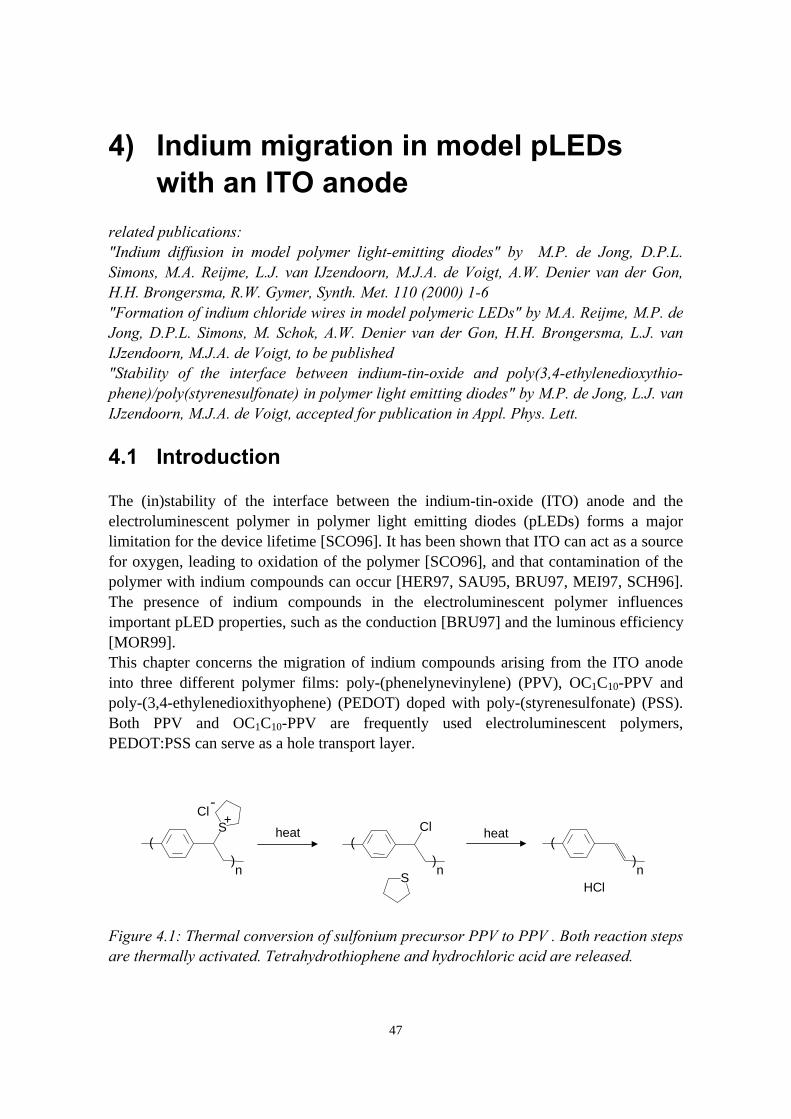
47
4) Indium migration in model pLEDswith an ITO anode
related publications:"Indium diffusion in model polymer light-emitting diodes" by M.P. de Jong, D.P.L.Simons, M.A. Reijme, L.J. van IJzendoorn, M.J.A. de Voigt, A.W. Denier van der Gon,H.H. Brongersma, R.W. Gymer, Synth. Met. 110 (2000) 1-6"Formation of indium chloride wires in model polymeric LEDs" by M.A. Reijme, M.P. deJong, D.P.L. Simons, M. Schok, A.W. Denier van der Gon, H.H. Brongersma, L.J. vanIJzendoorn, M.J.A. de Voigt, to be published"Stability of the interface between indium-tin-oxide and poly(3,4-ethylenedioxythio-phene)/poly(styrenesulfonate) in polymer light emitting diodes" by M.P. de Jong, L.J. vanIJzendoorn, M.J.A. de Voigt, accepted for publication in Appl. Phys. Lett.
4.1 Introduction
The (in)stability of the interface between the indium-tin-oxide (ITO) anode and theelectroluminescent polymer in polymer light emitting diodes (pLEDs) forms a majorlimitation for the device lifetime [SCO96]. It has been shown that ITO can act as a sourcefor oxygen, leading to oxidation of the polymer [SCO96], and that contamination of thepolymer with indium compounds can occur [HER97, SAU95, BRU97, MEI97, SCH96].The presence of indium compounds in the electroluminescent polymer influencesimportant pLED properties, such as the conduction [BRU97] and the luminous efficiency[MOR99].This chapter concerns the migration of indium compounds arising from the ITO anodeinto three different polymer films: poly-(phenelynevinylene) (PPV), OC1C10-PPV andpoly-(3,4-ethylenedioxithyophene) (PEDOT) doped with poly-(styrenesulfonate) (PSS).Both PPV and OC1C10-PPV are frequently used electroluminescent polymers,PEDOT:PSS can serve as a hole transport layer.
SHCl
S(
)n
Cl(
)n
(
)n
heat heat
Cl-
+
Figure 4.1: Thermal conversion of sulfonium precursor PPV to PPV . Both reaction stepsare thermally activated. Tetrahydrothiophene and hydrochloric acid are released.
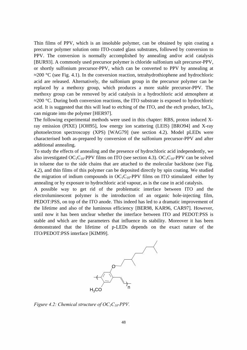
48
Thin films of PPV, which is an insoluble polymer, can be obtained by spin coating aprecursor polymer solution onto ITO-coated glass substrates, followed by conversion toPPV. The conversion is normally accomplished by annealing and/or acid catalysis[BUR93]. A commonly used precursor polymer is chloride sulfonium salt precursor-PPV,or shortly sulfonium precursor-PPV, which can be converted to PPV by annealing at≈200 °C (see Fig. 4.1). In the conversion reaction, tetrahydrothiophene and hydrochloricacid are released. Alternatively, the sulfonium group in the precursor polymer can bereplaced by a methoxy group, which produces a more stable precursor-PPV. Themethoxy group can be removed by acid catalysis in a hydrochloric acid atmosphere at≈200 °C. During both conversion reactions, the ITO substrate is exposed to hydrochloricacid. It is suggested that this will lead to etching of the ITO, and the etch product, InCl3,can migrate into the polymer [HER97].The following experimental methods were used in this chapter: RBS, proton induced X-ray emission (PIXE) [JOH95], low energy ion scattering (LEIS) [BRO94] and X-rayphotoelectron spectroscopy (XPS) [WAG79] (see section 4.2). Model pLEDs werecharacterised both as-prepared by conversion of the sulfonium precursor-PPV and afteradditional annealing.To study the effects of annealing and the presence of hydrochloric acid independently, wealso investigated OC1C10-PPV films on ITO (see section 4.3). OC1C10-PPV can be solvedin toluene due to the side chains that are attached to the molecular backbone (see Fig.4.2), and thin films of this polymer can be deposited directly by spin coating. We studiedthe migration of indium compounds in OC1C10-PPV films on ITO stimulated either byannealing or by exposure to hydrochloric acid vapour, as is the case in acid catalysis.A possible way to get rid of the problematic interface between ITO and theelectroluminescent polymer is the introduction of an organic hole-injecting film,PEDOT:PSS, on top of the ITO anode. This indeed has led to a dramatic improvement ofthe lifetime and also of the luminous efficiency [BER98, KAR96, CAR97]. However,until now it has been unclear whether the interface between ITO and PEDOT:PSS isstable and which are the parameters that influence its stability. Moreover it has beendemonstrated that the lifetime of p-LEDs depends on the exact nature of theITO/PEDOT:PSS interface [KIM99].
H3CO
O
(
)n
Figure 4.2: Chemical structure of OC1C10-PPV.
49
Due to the strong acidic nature of PSS, the aqueous solution from which the PEDOT:PSSfilms are normally cast can also be expected to etch the ITO. We investigated themigration of indium containing species into the PEDOT:PSS and overlying OC1C10-PPVfilms of model pLEDs using RBS (see section 4.4).
4.2 The migration of indium into sulfonium precursor-route PPV deposited on ITO
4.2.1 Sample preparation and experimental methods
Preparation of the model polymer light emitting diodesThe model pLEDs were prepared at Cavendish Laboratory, University of Cambridgeaccording to the following procedure. ITO-coated glass substrates (Baltracon, 30 Ω/o)were cleaned in ultrasonic baths of acetone and isopropanol, for 10 minutes each.Subsequently, a solution of 2 wt.% sulfonium precursor PPV (Cambridge DisplayTechnology) in methanol was spin coated onto the substrates under ambient conditions.After depositing the precursor polymer, the samples were transferred to a vacuumchamber installed in a glove box with a nitrogen atmosphere. Inside the vacuum chamber,the precursor polymer was thermally converted to PPV (see Fig. 4.1) by annealing atapproximately 240 °C for 10 hours. The so obtained PPV films were estimated to be 200nm thick. Finally, a 20 nm aluminium cathode was deposited by evaporation through amask, such that about half of the sample area was covered by aluminium. Inside the glovebox, the model pLEDs were packaged in sealed boxes for transport to Eindhoven. AtEindhoven University of Technology, the samples were stored in a glove box with anargon atmosphere.
RBS measurementsThe depth distribution of indium in the model pLEDs was measured with RBS, using a 2MeV He+ beam. For each sample, measurements were carried out on a region that wascovered with the aluminium cathode as well as on an uncovered region.Because the experiments described in this section were carried out before theconstruction of the cryogenic RBS/ERDA setup had been completed, all measurementswere performed at room temperature using the RBS ion channeling setup [DIJ97].Therefore, degradation of the polymer films due to ion irradiation had to be consideredcarefully.Since indium is a non-volatile element in room temperature RBS experiments, depthprofiling of indium can be performed, provided that no gas bubble formation occursunder the aluminium cathode (see section 3.4). In section 3.4, it was demonstrated thatroom temperature RBS measurements on OC1C10-PPV films covered with aluminium arevirtually impossible due to gas bubble formation.
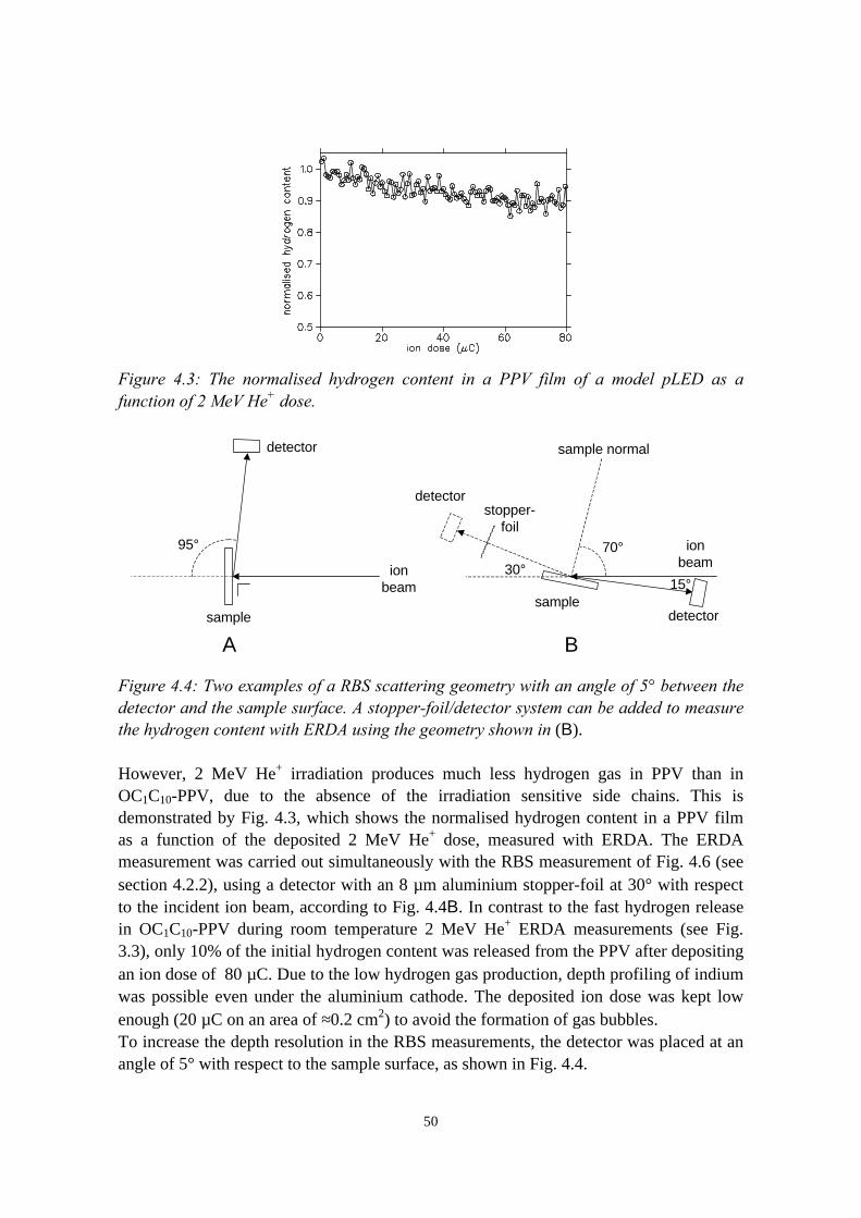
50
Figure 4.3: The normalised hydrogen content in a PPV film of a model pLED as afunction of 2 MeV He+ dose.
detector
ionbeam
samplesample
95° 70°
15°
ionbeam
detector
A B
30°
detectorstopper-
foil
sample normal
Figure 4.4: Two examples of a RBS scattering geometry with an angle of 5° between thedetector and the sample surface. A stopper-foil/detector system can be added to measurethe hydrogen content with ERDA using the geometry shown in (B).
However, 2 MeV He+ irradiation produces much less hydrogen gas in PPV than inOC1C10-PPV, due to the absence of the irradiation sensitive side chains. This isdemonstrated by Fig. 4.3, which shows the normalised hydrogen content in a PPV filmas a function of the deposited 2 MeV He+ dose, measured with ERDA. The ERDAmeasurement was carried out simultaneously with the RBS measurement of Fig. 4.6 (seesection 4.2.2), using a detector with an 8 µm aluminium stopper-foil at 30° with respectto the incident ion beam, according to Fig. 4.4B. In contrast to the fast hydrogen releasein OC1C10-PPV during room temperature 2 MeV He+ ERDA measurements (see Fig.3.3), only 10% of the initial hydrogen content was released from the PPV after depositingan ion dose of 80 µC. Due to the low hydrogen gas production, depth profiling of indiumwas possible even under the aluminium cathode. The deposited ion dose was kept lowenough (20 µC on an area of ≈0.2 cm2) to avoid the formation of gas bubbles.To increase the depth resolution in the RBS measurements, the detector was placed at anangle of 5° with respect to the sample surface, as shown in Fig. 4.4.
51
PIXE measurements, preparation of free-standing PPV filmsThe amount of precursor residues in the PPV films was measured with PIXE, using ourmicroprobe setup [MUT95] with a 3 MeV proton beam. The PIXE technique was chosenfor its good detection sensitivity for chlorine and sulphur (ppm detection limit), which areboth present in the leaving groups that are formed in the conversion reaction (see Fig.4.1). PIXE can thus be used as a sensitive tool for the detection of precursor residues.These residues could either be precursor polymer groups or leaving groups that weredetached from the polymer chain but have not left the PPV film. In contrast to the non-volatile element In, Cl is released from the material during ion bombardment. Thechlorine content was determined by measuring the Cl-K X-ray yield as a function of thedeposited ion dose and subsequent extrapolation to zero dose.PIXE analysis of Cl and S in the polymer layer of a model pLED would be distorted bysignals from the thick glass substrate. Therefore, free-standing PPV films were preparedby casting the precursor solution onto polytetrafluoroethylene (PTFE), followed bythermal conversion using similar conditions as for the model pLEDs. The converted filmscould easily be peeled off the PTFE substrate.The free-standing films are several microns thick, which is much thicker than the PPVlayers in the model LEDs. This implies that the conversion efficiency might be lower forthese free-standing films, and the amount of precursor residues in these films can beregarded as an upper limit for the amount of precursor residues in the converted modelLEDs.
LEIS and XPS measurementsLEIS and XPS were used to study the elemental composition of the surface region of thepLEDs. The experiments were performed with the ERISS setup [BER96]. This machineis equipped with a double toroidal electrostatic analyser and position sensitive detectorwhich can be used to detect either ions (LEIS) or electrons (XPS). For LEIS, a 3 keV3He+ beam was directed perpendicular to the sample surface, and the energy spectrum ofions backscattered at 145° was measured. The ion doses used were below 1014 ions/cm2,which is for 3He+ ions low enough to prevent influence of the measurement by ion beaminduced damage. Due to the strong neutralisation of the 3He+ ions, the backscattered ionsoriginate almost exclusively from scattering from the outermost layer of the solid, andthus the LEIS spectrum represents the elemental composition of the outermost layer.The XPS spectra were obtained using Mg-Kα radiation at 1253.6 eV from a VG twinanode X-ray source. The sample was tilted at an angle of 45° with respect to the X-raysource and analyser. The XPS spectra were used to obtain the elemental composition in aregion near the surface of which the thickness is determined by the inelastic mean freepath of the photoelectrons, and is between 3 and 10 nm depending on the kinetic energyof the photoelectron. For both LEIS and XPS the sample was sprayed with low energyelectrons to prevent charging.
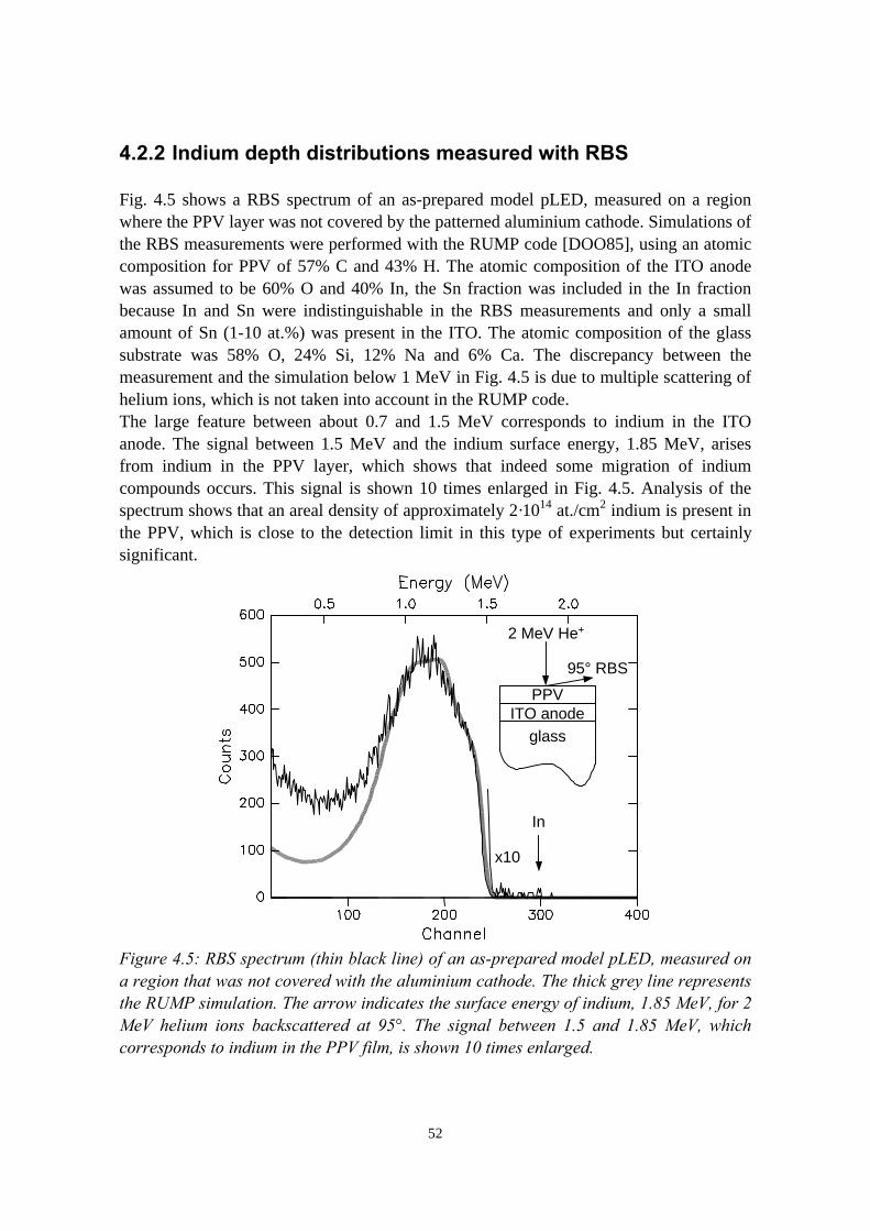
52
4.2.2 Indium depth distributions measured with RBS
Fig. 4.5 shows a RBS spectrum of an as-prepared model pLED, measured on a regionwhere the PPV layer was not covered by the patterned aluminium cathode. Simulations ofthe RBS measurements were performed with the RUMP code [DOO85], using an atomiccomposition for PPV of 57% C and 43% H. The atomic composition of the ITO anodewas assumed to be 60% O and 40% In, the Sn fraction was included in the In fractionbecause In and Sn were indistinguishable in the RBS measurements and only a smallamount of Sn (1-10 at.%) was present in the ITO. The atomic composition of the glasssubstrate was 58% O, 24% Si, 12% Na and 6% Ca. The discrepancy between themeasurement and the simulation below 1 MeV in Fig. 4.5 is due to multiple scattering ofhelium ions, which is not taken into account in the RUMP code.The large feature between about 0.7 and 1.5 MeV corresponds to indium in the ITOanode. The signal between 1.5 MeV and the indium surface energy, 1.85 MeV, arisesfrom indium in the PPV layer, which shows that indeed some migration of indiumcompounds occurs. This signal is shown 10 times enlarged in Fig. 4.5. Analysis of thespectrum shows that an areal density of approximately 2·1014 at./cm2 indium is present inthe PPV, which is close to the detection limit in this type of experiments but certainlysignificant.
glass
ITO anodePPV
2 MeV He+
95° RBS
In
x10
Figure 4.5: RBS spectrum (thin black line) of an as-prepared model pLED, measured ona region that was not covered with the aluminium cathode. The thick grey line representsthe RUMP simulation. The arrow indicates the surface energy of indium, 1.85 MeV, for 2MeV helium ions backscattered at 95°. The signal between 1.5 and 1.85 MeV, whichcorresponds to indium in the PPV film, is shown 10 times enlarged.
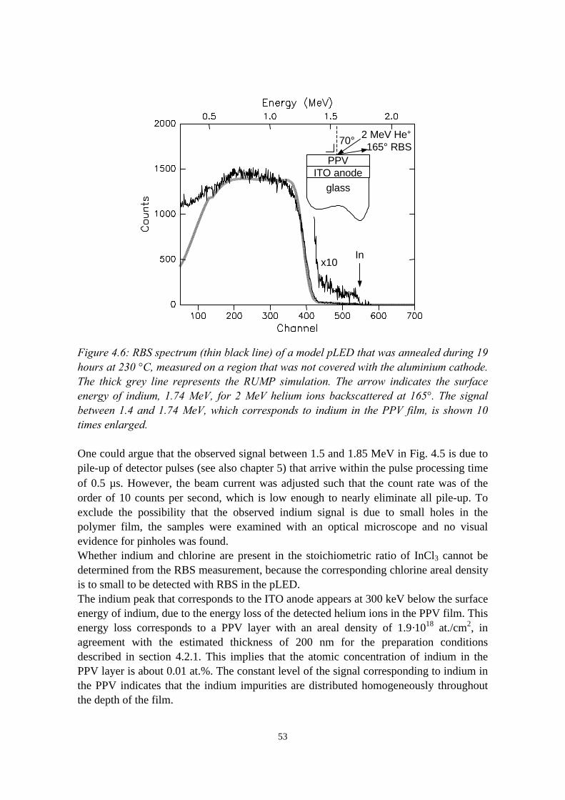
53
glass
ITO anodePPV
2 MeV He+
165° RBS70°
Inx10
Figure 4.6: RBS spectrum (thin black line) of a model pLED that was annealed during 19hours at 230 °C, measured on a region that was not covered with the aluminium cathode.The thick grey line represents the RUMP simulation. The arrow indicates the surfaceenergy of indium, 1.74 MeV, for 2 MeV helium ions backscattered at 165°. The signalbetween 1.4 and 1.74 MeV, which corresponds to indium in the PPV film, is shown 10times enlarged.
One could argue that the observed signal between 1.5 and 1.85 MeV in Fig. 4.5 is due topile-up of detector pulses (see also chapter 5) that arrive within the pulse processing timeof 0.5 µs. However, the beam current was adjusted such that the count rate was of theorder of 10 counts per second, which is low enough to nearly eliminate all pile-up. Toexclude the possibility that the observed indium signal is due to small holes in thepolymer film, the samples were examined with an optical microscope and no visualevidence for pinholes was found.Whether indium and chlorine are present in the stoichiometric ratio of InCl3 cannot bedetermined from the RBS measurement, because the corresponding chlorine areal densityis to small to be detected with RBS in the pLED.The indium peak that corresponds to the ITO anode appears at 300 keV below the surfaceenergy of indium, due to the energy loss of the detected helium ions in the PPV film. Thisenergy loss corresponds to a PPV layer with an areal density of 1.9·1018 at./cm2, inagreement with the estimated thickness of 200 nm for the preparation conditionsdescribed in section 4.2.1. This implies that the atomic concentration of indium in thePPV layer is about 0.01 at.%. The constant level of the signal corresponding to indium inthe PPV indicates that the indium impurities are distributed homogeneously throughoutthe depth of the film.
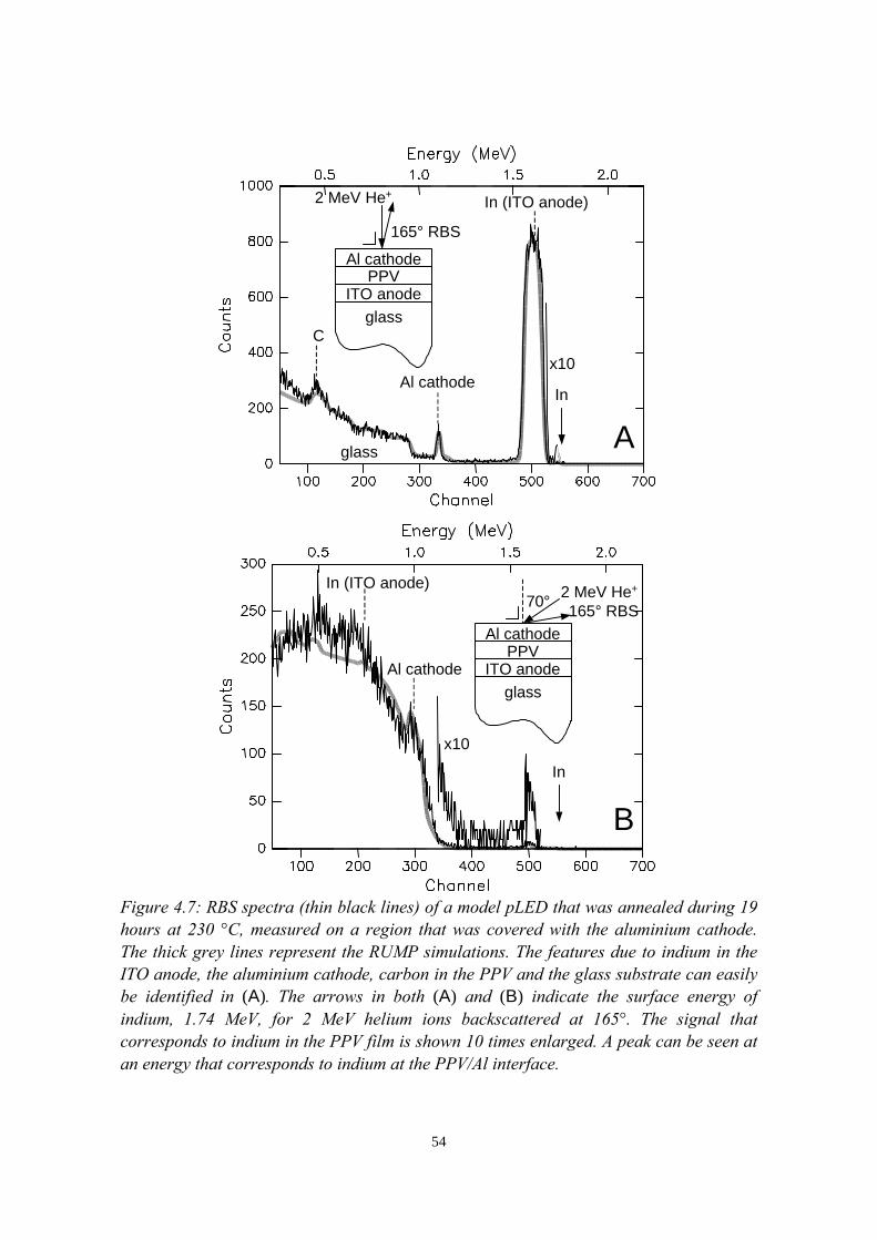
54
2 MeV He+
165° RBS
PPV
glass
ITO anode
Al cathode
In
x10
In (ITO anode)
Al cathode
C
glassA
2 MeV He+
165° RBS70°
glass
ITO anodePPV
Al cathode
In
x10
In (ITO anode)
Al cathode
B
Figure 4.7: RBS spectra (thin black lines) of a model pLED that was annealed during 19hours at 230 °C, measured on a region that was covered with the aluminium cathode.The thick grey lines represent the RUMP simulations. The features due to indium in theITO anode, the aluminium cathode, carbon in the PPV and the glass substrate can easilybe identified in (A). The arrows in both (A) and (B) indicate the surface energy ofindium, 1.74 MeV, for 2 MeV helium ions backscattered at 165°. The signal thatcorresponds to indium in the PPV film is shown 10 times enlarged. A peak can be seen atan energy that corresponds to indium at the PPV/Al interface.
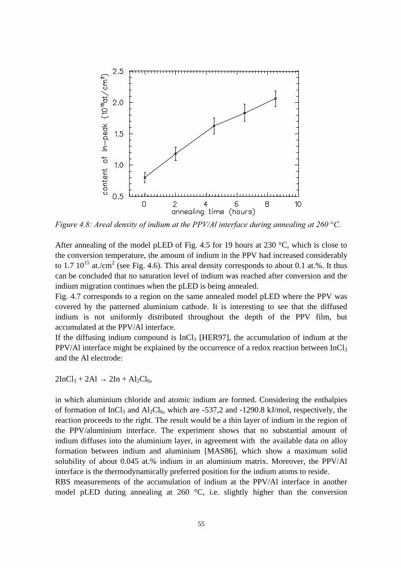
55
Figure 4.8: Areal density of indium at the PPV/Al interface during annealing at 260 °C.
After annealing of the model pLED of Fig. 4.5 for 19 hours at 230 °C, which is close tothe conversion temperature, the amount of indium in the PPV had increased considerablyto 1.7 1015 at./cm2 (see Fig. 4.6). This areal density corresponds to about 0.1 at.%. It thuscan be concluded that no saturation level of indium was reached after conversion and theindium migration continues when the pLED is being annealed.Fig. 4.7 corresponds to a region on the same annealed model pLED where the PPV wascovered by the patterned aluminium cathode. It is interesting to see that the diffusedindium is not uniformly distributed throughout the depth of the PPV film, butaccumulated at the PPV/Al interface.If the diffusing indium compound is InCl3 [HER97], the accumulation of indium at thePPV/Al interface might be explained by the occurrence of a redox reaction between InCl3
and the Al electrode:
2InCl3 + 2Al → 2In + Al2Cl6,
in which aluminium chloride and atomic indium are formed. Considering the enthalpiesof formation of InCl3 and Al2Cl6, which are -537,2 and -1290.8 kJ/mol, respectively, thereaction proceeds to the right. The result would be a thin layer of indium in the region ofthe PPV/aluminium interface. The experiment shows that no substantial amount ofindium diffuses into the aluminium layer, in agreement with the available data on alloyformation between indium and aluminium [MAS86], which show a maximum solidsolubility of about 0.045 at.% indium in an aluminium matrix. Moreover, the PPV/Alinterface is the thermodynamically preferred position for the indium atoms to reside.RBS measurements of the accumulation of indium at the PPV/Al interface in anothermodel pLED during annealing at 260 °C, i.e. slightly higher than the conversion
56
temperature, show that the process does not terminate even when the amount of indiumatoms at the interface exceeds the amount of indium corresponding to a monolayer (≈1015
at./cm2). This can be seen in Fig. 4.8, which shows the content of the peak of indium atthe PPV/Al interface as a function of annealing time. The indium atoms may not form aclosed monolayer. Alternatively, after completion of a closed monolayer, the reactioncould still proceed via chemically induced segregation of Al through In, thanks to thepresence of Cl at the interface.
4.2.3 Quantification of precursor residues with PIXE
During annealing of the model pLEDs, thermal conversion of precursor residues can leadto the production of hydrochloric acid which would further erode the ITO electrode. Theimportance of this effect depends on the amount of retained precursor residues in the PPVfilms. PIXE analyses showed that the retained chlorine and sulphur contents in the freestanding films are typically 0.1 at.% and 0.01 at.%, respectively. In sulfonium precursorPPV (see Fig. 4.1), the atomic percentage of both chlorine and sulphur is approximately 4at.%. A difference between the chlorine and sulphur content after conversion could beexpected, since the tetrahydrothiophene group leaves the material after the firstconversion step, whereas the hydrochloric acid is produced in the second step. Since thedifference between the chlorine and sulphur contents is so large, we can assume that mosttetrahydrothiophene groups are removed. Consequently, the polymer is assumed to be ofthe form (C8H6)n(C8H7Cl)m. Since the chlorine content is 0.1 at.%, it follows that the ratioof n and m is 66:1, which implies that approximately 98% of the material is fullyconverted.Trace amounts (between 1 and 100 ppm) of Si, K, Na, Al and Ar were also found in thefree-standing films. The Ar impurity arises from the Ar atmosphere in the glove box inwhich the films were stored.It is interesting to compare the Cl concentration measured in free standing films with theamount of In present in the model pLEDs after annealing. In that respect it is important torealise that the Cl concentration in the free standing films can be considered as an upperlimit of the chlorine concentration in the model pLED. If nevertheless the model structurewould contain the full 0.1 at.% Cl, this would correspond to ≈ 2⋅1015 at./cm2 Cl. Thisareal density will be released in the form of HCl upon further annealing of the modelpLED and a fraction is expected to react with the ITO. On the other hand, in section 4.3 itwill be demonstrated that indium and chlorine are present in the stoichiometric ratio ofInCl3 in OC1C10-PPV films on ITO that were exposed to HCl (see section 4.3). The RBSanalyses revealed an indium areal density of ≈1.7⋅1015 at./cm2 in the film after 19 hoursannealing at 230 °C and > 2⋅1015 at./cm2 indium present at the PPV/Al interface after 8hours annealing at 260 °C (see Fig 4.8). Consequently, the InCl3 in the PPV cannot befully attributed to originate from a reaction of the 0.1 at.% Cl released during theannealing experiments but must be associated with a reservoir of InCl3 formed at theITO/PPV interface by the initial conversion step.
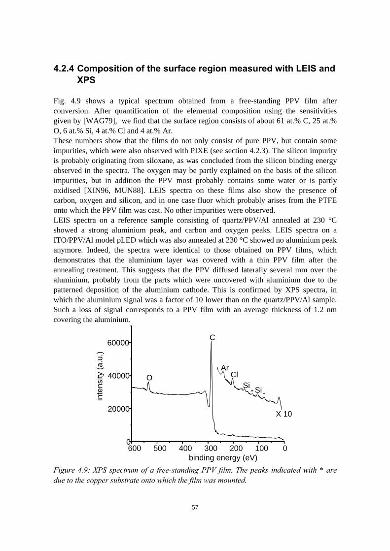
57
4.2.4 Composition of the surface region measured with LEIS andXPS
Fig. 4.9 shows a typical spectrum obtained from a free-standing PPV film afterconversion. After quantification of the elemental composition using the sensitivitiesgiven by [WAG79], we find that the surface region consists of about 61 at.% C, 25 at.%O, 6 at.% Si, 4 at.% Cl and 4 at.% Ar.These numbers show that the films do not only consist of pure PPV, but contain someimpurities, which were also observed with PIXE (see section 4.2.3). The silicon impurityis probably originating from siloxane, as was concluded from the silicon binding energyobserved in the spectra. The oxygen may be partly explained on the basis of the siliconimpurities, but in addition the PPV most probably contains some water or is partlyoxidised [XIN96, MUN88]. LEIS spectra on these films also show the presence ofcarbon, oxygen and silicon, and in one case fluor which probably arises from the PTFEonto which the PPV film was cast. No other impurities were observed.LEIS spectra on a reference sample consisting of quartz/PPV/Al annealed at 230 °Cshowed a strong aluminium peak, and carbon and oxygen peaks. LEIS spectra on aITO/PPV/Al model pLED which was also annealed at 230 °C showed no aluminium peakanymore. Indeed, the spectra were identical to those obtained on PPV films, whichdemonstrates that the aluminium layer was covered with a thin PPV film after theannealing treatment. This suggests that the PPV diffused laterally several mm over thealuminium, probably from the parts which were uncovered with aluminium due to thepatterned deposition of the aluminium cathode. This is confirmed by XPS spectra, inwhich the aluminium signal was a factor of 10 lower than on the quartz/PPV/Al sample.Such a loss of signal corresponds to a PPV film with an average thickness of 1.2 nmcovering the aluminium.
ClAr
∗Si
Si
X 10
600 500 400 300 200 100 00
20000
40000
60000
binding energy (eV)
O
C
∗
inte
nsity
(a.
u.)
Figure 4.9: XPS spectrum of a free-standing PPV film. The peaks indicated with ∗ aredue to the copper substrate onto which the film was mounted.
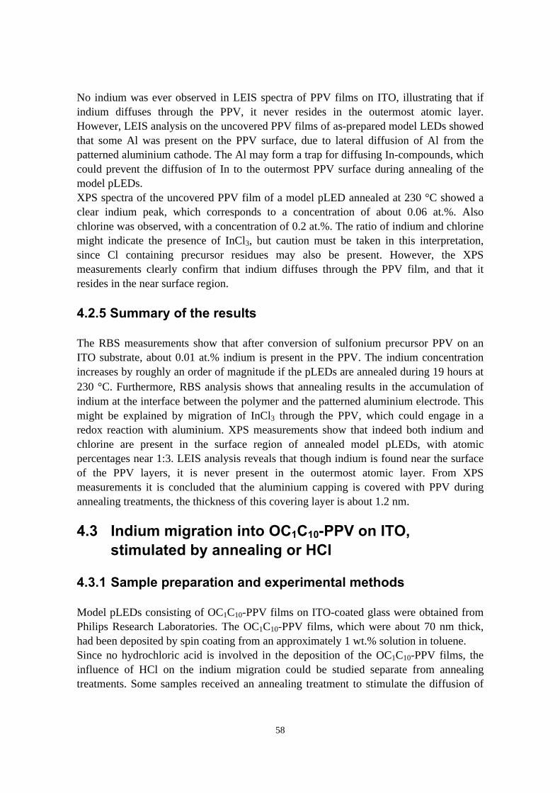
58
No indium was ever observed in LEIS spectra of PPV films on ITO, illustrating that ifindium diffuses through the PPV, it never resides in the outermost atomic layer.However, LEIS analysis on the uncovered PPV films of as-prepared model LEDs showedthat some Al was present on the PPV surface, due to lateral diffusion of Al from thepatterned aluminium cathode. The Al may form a trap for diffusing In-compounds, whichcould prevent the diffusion of In to the outermost PPV surface during annealing of themodel pLEDs.XPS spectra of the uncovered PPV film of a model pLED annealed at 230 °C showed aclear indium peak, which corresponds to a concentration of about 0.06 at.%. Alsochlorine was observed, with a concentration of 0.2 at.%. The ratio of indium and chlorinemight indicate the presence of InCl3, but caution must be taken in this interpretation,since Cl containing precursor residues may also be present. However, the XPSmeasurements clearly confirm that indium diffuses through the PPV film, and that itresides in the near surface region.
4.2.5 Summary of the results
The RBS measurements show that after conversion of sulfonium precursor PPV on anITO substrate, about 0.01 at.% indium is present in the PPV. The indium concentrationincreases by roughly an order of magnitude if the pLEDs are annealed during 19 hours at230 °C. Furthermore, RBS analysis shows that annealing results in the accumulation ofindium at the interface between the polymer and the patterned aluminium electrode. Thismight be explained by migration of InCl3 through the PPV, which could engage in aredox reaction with aluminium. XPS measurements show that indeed both indium andchlorine are present in the surface region of annealed model pLEDs, with atomicpercentages near 1:3. LEIS analysis reveals that though indium is found near the surfaceof the PPV layers, it is never present in the outermost atomic layer. From XPSmeasurements it is concluded that the aluminium capping is covered with PPV duringannealing treatments, the thickness of this covering layer is about 1.2 nm.
4.3 Indium migration into OC1C10-PPV on ITO,stimulated by annealing or HCl
4.3.1 Sample preparation and experimental methods
Model pLEDs consisting of OC1C10-PPV films on ITO-coated glass were obtained fromPhilips Research Laboratories. The OC1C10-PPV films, which were about 70 nm thick,had been deposited by spin coating from an approximately 1 wt.% solution in toluene.Since no hydrochloric acid is involved in the deposition of the OC1C10-PPV films, theinfluence of HCl on the indium migration could be studied separate from annealingtreatments. Some samples received an annealing treatment to stimulate the diffusion of
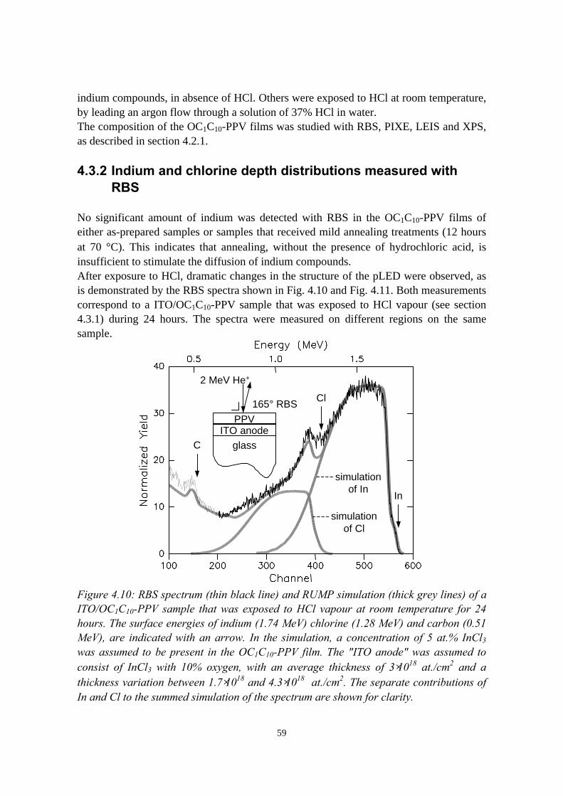
59
indium compounds, in absence of HCl. Others were exposed to HCl at room temperature,by leading an argon flow through a solution of 37% HCl in water.The composition of the OC1C10-PPV films was studied with RBS, PIXE, LEIS and XPS,as described in section 4.2.1.
4.3.2 Indium and chlorine depth distributions measured withRBS
No significant amount of indium was detected with RBS in the OC1C10-PPV films ofeither as-prepared samples or samples that received mild annealing treatments (12 hoursat 70 °C). This indicates that annealing, without the presence of hydrochloric acid, isinsufficient to stimulate the diffusion of indium compounds.After exposure to HCl, dramatic changes in the structure of the pLED were observed, asis demonstrated by the RBS spectra shown in Fig. 4.10 and Fig. 4.11. Both measurementscorrespond to a ITO/OC1C10-PPV sample that was exposed to HCl vapour (see section4.3.1) during 24 hours. The spectra were measured on different regions on the samesample.
2 MeV He+
165° RBS
PPV
glass
ITO anode
In
Cl
C
simulationof In
simulationof Cl
Figure 4.10: RBS spectrum (thin black line) and RUMP simulation (thick grey lines) of aITO/OC1C10-PPV sample that was exposed to HCl vapour at room temperature for 24hours. The surface energies of indium (1.74 MeV) chlorine (1.28 MeV) and carbon (0.51MeV), are indicated with an arrow. In the simulation, a concentration of 5 at.% InCl3
was assumed to be present in the OC1C10-PPV film. The "ITO anode" was assumed toconsist of InCl3 with 10% oxygen, with an average thickness of 3⋅1018 at./cm2 and athickness variation between 1.7⋅1018 and 4.3⋅1018 at./cm2. The separate contributions ofIn and Cl to the summed simulation of the spectrum are shown for clarity.
60
2 MeV He+
165° RBS
PPV
glass
ITO anode
InCl
C
Figure 4.11: RBS spectrum (thin black line) and RUMP simulation (thick grey line) of aITO/OC1C10-PPV sample that was exposed to HCl vapour at room temperature for 24hours. The surface energies of indium (1.74 MeV) chlorine (1.28 MeV) and carbon (0.51MeV), are indicated with an arrow. In the simulation, a concentration of 3% InCl3 wasassumed to be present in the OC1C10-PPV film. The "ITO anode" was assumed to consistof InCl3 with 10% oxygen, with an average thickness of 6.5⋅1017 at./cm2 and a thicknessvariation between 0 and 1.85⋅1018 at./cm2.
The exposure to HCl vapour is of course quite drastic, but similar treatments are used inthe acid catalysis of some precursor polymers. Acid catalysis is usually carried out at≈200 °C, which results in the removal of water from the organic films. The presence ofwater in combination with hydrochloric acid during the room temperature exposure willmost probably accelerate the erosion of the ITO anode.The measurements show that the ITO anode has been largely converted into a layer witha stoichiometric In/Cl ratio of ≈1/3 due to the reaction with HCl. This can be seen fromthe large chlorine feature at an energy that corresponds to the former location of the ITOanode (see Fig. 4.11). The converted ITO layer is far from homogeneous (see also section4.3.3), which results in strong tailing of the indium and chlorine features. Moreover, atotally different average thickness of the layer is observed in Fig. 4.10 compared to Fig.4.11. Some inhomogeneities could even be spotted with the naked eye, as small bubbleson the sample surface. Using RUMP, the "ITO anode" was simulated as a layer with aspecified roughness. In this mode, the RUMP code calculates a summation of spectrawith a layer thickness varying between specified boundaries.
61
Although the OC1C10-PPV film still covers the converted ITO layer, the RBSmeasurements show that significant doping of the OC1C10-PPV occurs. The summedconcentration of In and Cl in the OC1C10-PPV roughly amounts to 5 at.% (!).The occurance of chemical doping of the OC1C10-PPV was also observed from adiscoloration of the film, from orange to green. This discoloration was only observed atthe lateral position on the sample where the patterned ITO anode was present, and couldtherefore not be attributed to a reaction between HCl and OC1C10-PPV.
4.3.3 PIXE, LEIS and XPS measurements
The OC1C10-PPV films of the samples that had been exposed to HCl were peeled off theITO-coated glass substrates using a 3M Scotch tape. The tape with the OC1C10-PPVcould be subsequently be analysed with scanning µPIXE, using our microprobe setupwith a 3 MeV proton beam. Both indium and chlorine were detected in the peeledOC1C10-PPV films, accumulated in islands of 10-100 µm [SIM98]. In the islands, In andCl were present in the stoichiometric ratio of InCl3, as was determined from comparisonof the PIXE spectra of the tape/OC1C10-PPV samples with the PIXE spectrum of an InCl3
salt.The surfaces of the HCl-exposed ITO/OC1C10-PPV samples were analysed with LEISand XPS [REI00]. The LEIS measurements, combined with sputtering, showed that bothindium and chlorine were present just beneath the outermost atomic layer of the OC1C10-PPV films, which again confirms that indium chloride compounds migrate through thepolymer. XPS measurements also show the presence of an indium chloride compound inthe near surface region of the films.
4.3.4 Summary of the results
Annealing of model pLEDs consisting of an OC1C10-PPV film on an ITO-coated glasssubstrate does not lead to significant migration of indium compounds into the OC1C10-PPV. Exposing the pLEDs to HCl vapour results in dramatic compositional changes,including the formation of InCl3 islands in the polymer. It can thus be concluded that thepresence of HCl in the polymer film causes much more erosion of the ITO anode andmigration of indium compounds than annealing.
4.4 The migration of indium into PEDOT:PSS films andPEDOT:PSS/PPV double layers deposited on ITO
4.4.1 Sample preparation and RBS measurements
PEDOT:PSS (see Fig. 4.12) films were prepared by spin coating an aqueous solution ofPEDOT:PSS [JON94] onto commercially available ITO-coated glass substrates (Merck
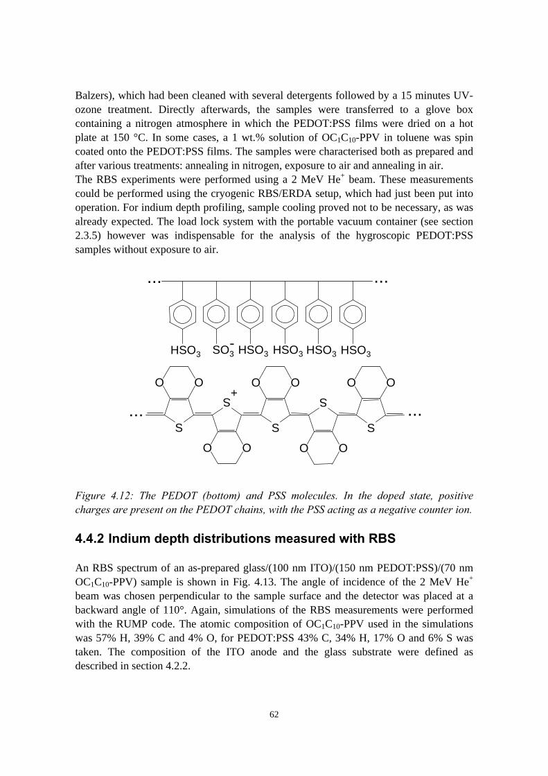
62
Balzers), which had been cleaned with several detergents followed by a 15 minutes UV-ozone treatment. Directly afterwards, the samples were transferred to a glove boxcontaining a nitrogen atmosphere in which the PEDOT:PSS films were dried on a hotplate at 150 °C. In some cases, a 1 wt.% solution of OC1C10-PPV in toluene was spincoated onto the PEDOT:PSS films. The samples were characterised both as prepared andafter various treatments: annealing in nitrogen, exposure to air and annealing in air.The RBS experiments were performed using a 2 MeV He+ beam. These measurementscould be performed using the cryogenic RBS/ERDA setup, which had just been put intooperation. For indium depth profiling, sample cooling proved not to be necessary, as wasalready expected. The load lock system with the portable vacuum container (see section2.3.5) however was indispensable for the analysis of the hygroscopic PEDOT:PSSsamples without exposure to air.
S
O O
SO3-
S+
O O
S
O OS
O O
S
O O
HSO3 HSO3HSO3 HSO3HSO3
......
... ...
Figure 4.12: The PEDOT (bottom) and PSS molecules. In the doped state, positivecharges are present on the PEDOT chains, with the PSS acting as a negative counter ion.
4.4.2 Indium depth distributions measured with RBS
An RBS spectrum of an as-prepared glass/(100 nm ITO)/(150 nm PEDOT:PSS)/(70 nmOC1C10-PPV) sample is shown in Fig. 4.13. The angle of incidence of the 2 MeV He+
beam was chosen perpendicular to the sample surface and the detector was placed at abackward angle of 110°. Again, simulations of the RBS measurements were performedwith the RUMP code. The atomic composition of OC1C10-PPV used in the simulationswas 57% H, 39% C and 4% O, for PEDOT:PSS 43% C, 34% H, 17% O and 6% S wastaken. The composition of the ITO anode and the glass substrate were defined asdescribed in section 4.2.2.
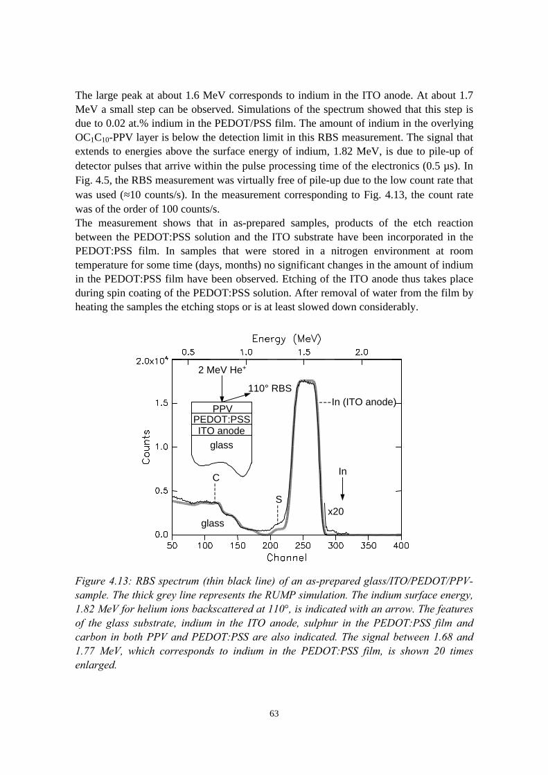
63
The large peak at about 1.6 MeV corresponds to indium in the ITO anode. At about 1.7MeV a small step can be observed. Simulations of the spectrum showed that this step isdue to 0.02 at.% indium in the PEDOT/PSS film. The amount of indium in the overlyingOC1C10-PPV layer is below the detection limit in this RBS measurement. The signal thatextends to energies above the surface energy of indium, 1.82 MeV, is due to pile-up ofdetector pulses that arrive within the pulse processing time of the electronics (0.5 µs). InFig. 4.5, the RBS measurement was virtually free of pile-up due to the low count rate thatwas used (≈10 counts/s). In the measurement corresponding to Fig. 4.13, the count ratewas of the order of 100 counts/s.The measurement shows that in as-prepared samples, products of the etch reactionbetween the PEDOT:PSS solution and the ITO substrate have been incorporated in thePEDOT:PSS film. In samples that were stored in a nitrogen environment at roomtemperature for some time (days, months) no significant changes in the amount of indiumin the PEDOT:PSS film have been observed. Etching of the ITO anode thus takes placeduring spin coating of the PEDOT:PSS solution. After removal of water from the film byheating the samples the etching stops or is at least slowed down considerably.
In
x20
In (ITO anode)
C
glass
ITO anodePEDOT:PSS
2 MeV He+
110° RBS
PPV
S
glass
Figure 4.13: RBS spectrum (thin black line) of an as-prepared glass/ITO/PEDOT/PPV-sample. The thick grey line represents the RUMP simulation. The indium surface energy,1.82 MeV for helium ions backscattered at 110°, is indicated with an arrow. The featuresof the glass substrate, indium in the ITO anode, sulphur in the PEDOT:PSS film andcarbon in both PPV and PEDOT:PSS are also indicated. The signal between 1.68 and1.77 MeV, which corresponds to indium in the PEDOT:PSS film, is shown 20 timesenlarged.
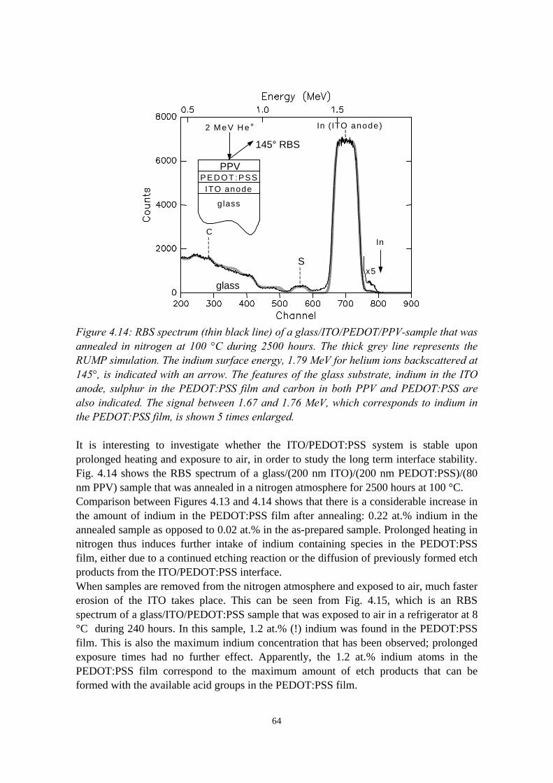
64
In
x5
In (ITO anode)
C
glass
ITO anodeP E D O T :PSS
2 M e V H e+
145° RBS
PPV
S
glass
Figure 4.14: RBS spectrum (thin black line) of a glass/ITO/PEDOT/PPV-sample that wasannealed in nitrogen at 100 °C during 2500 hours. The thick grey line represents theRUMP simulation. The indium surface energy, 1.79 MeV for helium ions backscattered at145°, is indicated with an arrow. The features of the glass substrate, indium in the ITOanode, sulphur in the PEDOT:PSS film and carbon in both PPV and PEDOT:PSS arealso indicated. The signal between 1.67 and 1.76 MeV, which corresponds to indium inthe PEDOT:PSS film, is shown 5 times enlarged.
It is interesting to investigate whether the ITO/PEDOT:PSS system is stable uponprolonged heating and exposure to air, in order to study the long term interface stability.Fig. 4.14 shows the RBS spectrum of a glass/(200 nm ITO)/(200 nm PEDOT:PSS)/(80nm PPV) sample that was annealed in a nitrogen atmosphere for 2500 hours at 100 °C.Comparison between Figures 4.13 and 4.14 shows that there is a considerable increase inthe amount of indium in the PEDOT:PSS film after annealing: 0.22 at.% indium in theannealed sample as opposed to 0.02 at.% in the as-prepared sample. Prolonged heating innitrogen thus induces further intake of indium containing species in the PEDOT:PSSfilm, either due to a continued etching reaction or the diffusion of previously formed etchproducts from the ITO/PEDOT:PSS interface.When samples are removed from the nitrogen atmosphere and exposed to air, much fastererosion of the ITO takes place. This can be seen from Fig. 4.15, which is an RBSspectrum of a glass/ITO/PEDOT:PSS sample that was exposed to air in a refrigerator at 8°C during 240 hours. In this sample, 1.2 at.% (!) indium was found in the PEDOT:PSSfilm. This is also the maximum indium concentration that has been observed; prolongedexposure times had no further effect. Apparently, the 1.2 at.% indium atoms in thePEDOT:PSS film correspond to the maximum amount of etch products that can beformed with the available acid groups in the PEDOT:PSS film.

65
glass
ITO anodePEDOT:PSS
2 MeV He+
110° RBS
In
C
S
glass
In (ITO anode)
Figure 4.15: RBS spectrum (thin black line) of a glass/ITO/PEDOT-sample that wasexposed to air during 240 hours in a refrigerator at 8 °C. The thick grey line representsthe RUMP simulation. The indium surface energy, 1.82 MeV for helium ionsbackscattered at 110°, is indicated with an arrow. The features of the glass substrate,indium in the ITO anode, and sulphur and carbon in the PEDOT:PSS film are alsoindicated. The step between 1.68 and 1.82 MeV corresponds to 1.2 at.% indium atoms inthe PEDOT:PSS film.
0
0.05
0.1
0.15
0.2
0.25
0.3
0.35
0 5 10 15 20
time [hours]
In c
on
ten
t (a
t%)
Figure 4.16: The In content in PEDOT:PSS films as a function of the time the films wereexposed to air.
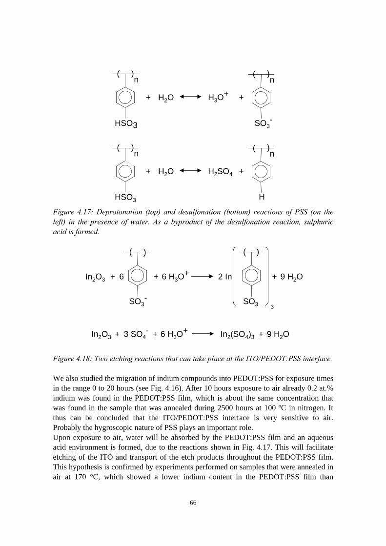
66
HSO3
( )n
H
( )n
H2SO4H2O+ +
HSO3
( )n
( )n
H3O+H2O+ +
SO3-
Figure 4.17: Deprotonation (top) and desulfonation (bottom) reactions of PSS (on theleft) in the presence of water. As a byproduct of the desulfonation reaction, sulphuricacid is formed.
9 H2O6 H3O++ +In2O3 + 3 SO4
- In2(SO4)3
SO3-
( )
+ +In2O3 6 H3O++ 6 2 In
SO3
(
3
9 H2O
)
Figure 4.18: Two etching reactions that can take place at the ITO/PEDOT:PSS interface.
We also studied the migration of indium compounds into PEDOT:PSS for exposure timesin the range 0 to 20 hours (see Fig. 4.16). After 10 hours exposure to air already 0.2 at.%indium was found in the PEDOT:PSS film, which is about the same concentration thatwas found in the sample that was annealed during 2500 hours at 100 ºC in nitrogen. Itthus can be concluded that the ITO/PEDOT:PSS interface is very sensitive to air.Probably the hygroscopic nature of PSS plays an important role.Upon exposure to air, water will be absorbed by the PEDOT:PSS film and an aqueousacid environment is formed, due to the reactions shown in Fig. 4.17. This will facilitateetching of the ITO and transport of the etch products throughout the PEDOT:PSS film.This hypothesis is confirmed by experiments performed on samples that were annealed inair at 170 °C, which showed a lower indium content in the PEDOT:PSS film than
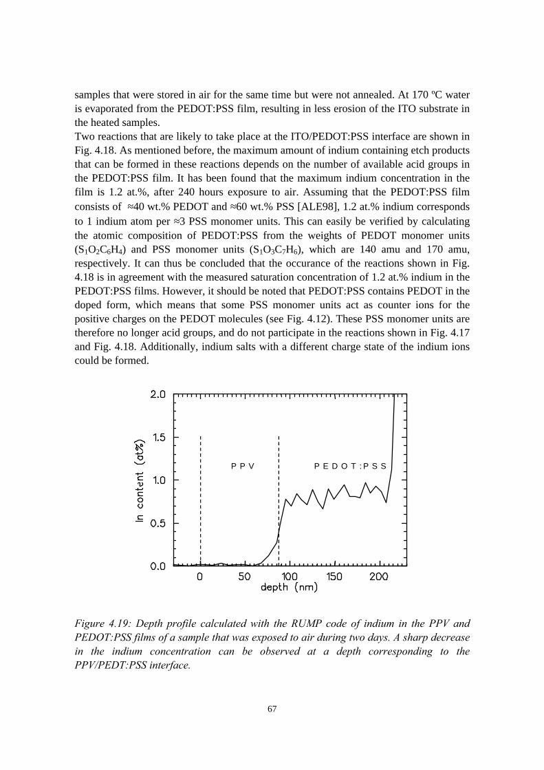
67
samples that were stored in air for the same time but were not annealed. At 170 ºC wateris evaporated from the PEDOT:PSS film, resulting in less erosion of the ITO substrate inthe heated samples.Two reactions that are likely to take place at the ITO/PEDOT:PSS interface are shown inFig. 4.18. As mentioned before, the maximum amount of indium containing etch productsthat can be formed in these reactions depends on the number of available acid groups inthe PEDOT:PSS film. It has been found that the maximum indium concentration in thefilm is 1.2 at.%, after 240 hours exposure to air. Assuming that the PEDOT:PSS filmconsists of ≈40 wt.% PEDOT and ≈60 wt.% PSS [ALE98], 1.2 at.% indium correspondsto 1 indium atom per ≈3 PSS monomer units. This can easily be verified by calculatingthe atomic composition of PEDOT:PSS from the weights of PEDOT monomer units(S1O2C6H4) and PSS monomer units (S1O3C7H6), which are 140 amu and 170 amu,respectively. It can thus be concluded that the occurance of the reactions shown in Fig.4.18 is in agreement with the measured saturation concentration of 1.2 at.% indium in thePEDOT:PSS films. However, it should be noted that PEDOT:PSS contains PEDOT in thedoped form, which means that some PSS monomer units act as counter ions for thepositive charges on the PEDOT molecules (see Fig. 4.12). These PSS monomer units aretherefore no longer acid groups, and do not participate in the reactions shown in Fig. 4.17and Fig. 4.18. Additionally, indium salts with a different charge state of the indium ionscould be formed.
P P V P E D O T : P S S
Figure 4.19: Depth profile calculated with the RUMP code of indium in the PPV andPEDOT:PSS films of a sample that was exposed to air during two days. A sharp decreasein the indium concentration can be observed at a depth corresponding to thePPV/PEDT:PSS interface.
68
The incorporation of indium salts in the PEDOT:PSS films might have consequences forthe electrical properties of the films. Although it is not likely that the indium salts affectthe charges on the PEDOT molecules, the conductivity of the films, which is mainlydetermined by hopping of charge carriers between isolated PEDOT clusters in a PSSmatrix [ALE98], may change. A possible relation between the presence of indiumcompounds in PEDOT:PSS and the electrical properties has not been investigated,although it has been reported that the lifetime of pLEDs depends on the exact propertiesof the ITO/PEDOT:PSS interface [KIM99].In samples that contained a PPV film on top of the PEDOT:PSS film, a rather sharpdecrease in the indium concentration was observed at a depth corresponding to thePEDOT:PSS/PPV interface (see Fig. 4.19). This implies that the indium containing etchproducts do not diffuse into the PPV film, but are trapped in the PEDOT:PSS layer, inagreement with the proposed etching mechanism.
4.4.3 Summary of the results
In spite of the increased performance of pLEDs with a PEDOT:PSS hole transport layer(see section 4.1), the RBS measurements show that the interface between ITO andPEDOT:PSS is not stable. In as-prepared samples already 0.02 at.% indium is present inthe PEDOT:PSS film due to etching of the ITO during spin coating. Annealing innitrogen at 100 °C leads to an increase in the indium concentration to 0.2 at.% after 2500hours. Exposure to air leads to a much more dramatic degradation of the interface; afterseveral days in air the amount of indium reaches a saturation concentration of 1.2 at.%.This demonstrates that due to the hygroscopic and acidic nature of PSS, theITO/PEDOT:PSS interface is extremely sensitive to the intake of water from theenvironment.
4.5 Conclusions
PPV films obtained by conversion of sulfonium precursor-PPV on ITO substrates containindium compounds, resulting from a chemical reaction between ITO and the conversionby-product HCl. RBS measurements show that after thermal conversion at 240 °C, about0.01 at.% indium is present in the PPV. Additional annealing for 19 hours at 230 °Cincreases the indium concentration to 0.1 at.%, mainly by diffusion of indium compoundsformed at the ITO/PPV interface in the initial conversion step. Furthermore, RBSanalysis shows that annealing results in the accumulation of indium at the interfacebetween the polymer and the patterned aluminium cathode. This might be explained bymigration of indium chloride through the PPV, followed by a chemical reaction betweenindium chloride and aluminium, in which atomic indium and aluminium chloride areformed.XPS measurements show that indeed both indium and chlorine are present in the surfaceregion of annealed model pLEDs, with atomic percentages near 1:3. LEIS analysis
69
reveals that though indium is found near the surface of the PPV layers, it is never presentin the outermost atomic layer.The crucial role played by HCl in the erosion of the ITO anode and the migration ofindium compounds into the overlying organic films becomes clear in the studies ofOC1C10-PPV films on ITO. Annealing of such samples caused no significant migration ofindium compounds into the OC1C10-PPV. However, exposure to HCl vapour led todramatic erosion of the ITO, accompanied by the formation of large (10-100 µm) InCl3
islands in the OC1C10-PPV film. It is known that indium chloride compounds can act asdopants in the electroluminescent polymer [BRU97], producing side-effects as increasedconductivity and quenching of luminescence.Although it has been found that the lifetime of pLEDs can be increased considerably bythe introduction of a PEDOT:PSS hole transport layer [BER98], the RBS measurementsshow that the interface between ITO and PEDOT:PSS is not stable. Again, thisdemonstrates the sensitivity of ITO to acids: due to the acidic nature of PSS, the aqueoussolution from which the PEDOT:PSS films is cast etches the ITO, and about 0.02 at.%indium is incorporated into the PEDOT:PSS. Annealing in nitrogen results in a gradualincrease of the indium concentration to 0.2 at.% after 2500 hours at 100 °C, either due toa continued etching reaction or the diffusion of previously formed etch products from theITO/PEDOT:PSS interface. Upon exposure to air, an aqueous acid environment iscreated in the PEDOT:PSS film due its hygroscopic nature. This results in fast etching ofthe ITO, after several days, a saturation concentration of 1.2 at.% indium is found in thePEDOT:PSS.
References
[ALE98] A.N. Aleshin, S.R. Williams, A.J. Heeger, Synth. Met. 94 (1998) 173[BER96] R.J. Bergmans, M. v.d. Grift, A.W. Denier van der Gon and H.H.
Brongersma, Surf. Sci. 345 (1996) 303[BER98] A. Berntsen, Y. Croonen, C. Liedenbaum, H. Schoo, R. J. Visser, J.
Vleggaar, and P. van de Weijer, Optical Materials 9 (1998) 125[BRU97] W. Brütting, M.Meier, M. Herold, S. Karg, M. Schwoerer, Chem. Phys.
227 (1997) 243[BRO94] H.H. Brongersma, P.A.C. Groenen, J.P. Jacobs, Application of low-energy
ion scattering to oxidic surfaces, Science of ceramic interfaces II, vol 81 ofMaterials Science Monographs, edited by J. Nowotny, (Elsevier,Amsterdam, 1994)
[BUR93] P.L. Burn, A. Kraft, D.R. Baigent, D.D.C. Bradley, A.R. Brown, R.H.Friend, R.W. Gymer, A.B. Holmes, R.W. Jackson, J. of the Am. Chem.Soc. 115 (1993) 10117
[CAR97] S.A. Carter, M. Angelopoulos, S. Karg, P.J. Brock, and J.C. Scott, Appl.Phys. Lett. 70 (1997) 2067
70
[DIJ97] P.W.L. van Dijk, A high-energy ion channelling facility and itsapplications, (PhD Dissertation, Eindhoven University of Technology,1997)
[DOO85] L.R. Doolittle, Nucl. Instr. and Meth. B 9 (1985) 344[HER97] M. Herold, J. Gmeiner, C. Drummer, M. Schwoerer, J. of Mat. Sci. 32
(1997) 5709[JOH95] S.A.E. Johannson, J.L. Campbell, K.G. Malmqvist, Particle induced X-ray
spectrometry, (Wiley, New York, 1995)[JON94] F. Jonas, W. Kraft, US Patent No. 5 300 575 (1994)[KAR96] S. Karg, J.C. Scott, J.R. Salem, and M. Angelopoulos, Synth. Met. 80
(1996) 111[KAR97] S. Karg, M. Meier, W. Riess, J. Appl. Phys. 82 (4) (1997) 1951[KIM99] J.S. Kim, R.H. Friend, and F. Cacialli, Appl. Phys. Lett. 74 (1999) 3084[MAS86] T.B. Massalski, Binary alloy phase diagrams, American Society for
Metals, Ohio (1986)[MEI97] M. Meier, S. Karg, W. Riess, J. Appl. Phys. 82 (4) (1997) 1961[MOR99] J. Morgado, F. Cacialli, J. Gruner, N.C. Greenham, R.H. Friend, J. Appl.
Phys. 85 (3) (1999) 1784[MUN88] H. Münstedt, Polymer 29 (1988) 296[MUT95] P.H.A. Mutsaers, Design and realisation of the Eindhoven scanning proton
microprobe, (PhD Dissertation, Eindhoven University of Technology,1995)
[REI00] M.A. Reijme, M.P. de Jong, D.P.L. Simons, M. Schok, A.W. Denier vander Gon, H.H. Brongersma, L.J. van IJzendoorn, M.J.A. de Voigt, to bepublished in J. Appl. Phys.
[SAU95] G.Sauer, M. Kilo, M. Hund , A. Wokaun, S. Karg, M. Meier, W. Riess, M.Schwoerer, H. Suzuki, J. Simmerer, H. Meyer, D. Haarer, J. Anal. Chem.353 (1995) 642
[SCH96] A.R. Schlatmann, D. Wilms Floet, A. Hilberer, F. Garten, P.J.M.Smulders, T.M. Klapwijk, G. Hadziioannou, Appl. Phys. Lett. 69 (1996)1764
[SCO96] J.C. Scott, J.H. Kaufman, P.J. Brock, R. DiPietro, J. Salem, and J. A.Goitia, J. Appl. Phys. 79 (1996) 2745
[SIM98] D.P.L. Simons, Data acquisition, detector technology and materialsanalysis with a scanning ion microprobe, (PhD Dissertation, EindhovenUniversity of Technology, 1998)
[WAG79] C.D. Wagner, W.M. Riggs, L.E. Davis, J.F.Moulder, G.E. Muilenberg,Handbook of X-ray photoelectron spectroscopy, (Perkin-ElmerCorporation, Norwalk, 1979)
[XIN96] K. Xing, M. Fahlman, M. Lögdlund, D.A. dos Santos, V. Parenté, R.Lazzaroni, J.L. Brédas, R.W. Gymer, W.R. Salaneck, Adv. Mater. 8 (12)(1996) 971
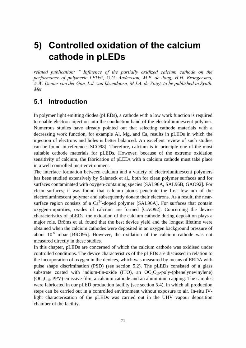
71
5) Controlled oxidation of the calciumcathode in pLEDs
related publication: " Influence of the partially oxidized calcium cathode on theperformance of polymeric LEDs", G.G. Andersson, M.P. de Jong, H.H. Brongersma,A.W. Denier van der Gon, L.J. van IJzendoorn, M.J.A. de Voigt, to be published in Synth.Met.
5.1 Introduction
In polymer light emitting diodes (pLEDs), a cathode with a low work function is requiredto enable electron injection into the conduction band of the electroluminescent polymer.Numerous studies have already pointed out that selecting cathode materials with adecreasing work function, for example Al, Mg, and Ca, results in pLEDs in which theinjection of electrons and holes is better balanced. An excellent review of such studiescan be found in reference [SCO98]. Therefore, calcium is in principle one of the mostsuitable cathode materials for pLEDs. However, because of the extreme oxidationsensitivity of calcium, the fabrication of pLEDs with a calcium cathode must take placein a well controlled inert environment.The interface formation between calcium and a variety of electroluminescent polymershas been studied extensively by Salaneck et al., both for clean polymer surfaces and forsurfaces contaminated with oxygen-containing species [SAL96A, SAL96B, GAO92]. Forclean surfaces, it was found that calcium atoms penetrate the first few nm of theelectroluminescent polymer and subsequently donate their electrons. As a result, the near-surface region consists of a Ca2+-doped polymer [SAL96A]. For surfaces that containoxygen-impurities, oxides of calcium are formed [GAO92]. Concerning the devicecharacteristics of pLEDs, the oxidation of the calcium cathode during deposition plays amajor role. Bröms et al. found that the best device yield and the longest lifetime wereobtained when the calcium cathodes were deposited in an oxygen background pressure ofabout 10-6 mbar [BRO95]. However, the oxidation of the calcium cathode was notmeasured directly in these studies.In this chapter, pLEDs are concerned of which the calcium cathode was oxidised undercontrolled conditions. The device characteristics of the pLEDs are discussed in relation tothe incorporation of oxygen in the devices, which was measured by means of ERDA withpulse shape discrimination (PSD) (see section 5.2). The pLEDs consisted of a glasssubstrate coated with indium-tin-oxide (ITO), an OC1C10-poly-(phenelynevinylene)(OC1C10-PPV) emissive film, a calcium cathode and an aluminium capping. The sampleswere fabricated in our pLED production facility (see section 5.4), in which all productionsteps can be carried out in a controlled environment without exposure to air. In-situ IV-light characterisation of the pLEDs was carried out in the UHV vapour depositionchamber of the facility.

72
Controlled oxidation of the calcium cathode was carried out in two different ways. In afirst series of pLEDs, thin calcium layers (0-80 nm) of semimanufactured devices wereexposed to oxygen gas, followed by the deposition of the remainder of the calciumcathode and the aluminium capping (see section 5.5.2). In a second series, the calciumcathode was deposited in a 10-8-10-5 mbar oxygen background pressure (see section5.5.3). The role played by residual water in the vapour deposition chamber is brieflydiscussed in section 5.6.
5.2 Oxygen depth profiling in pLEDs using ERDA withpulse shape discrimination (PSD)
One of the main problems in ERDA is the discrimination between the different recoilsand scattered beam particles that hit the detector. Quite a few discrimination techniqueshave been developed during the past decades, that rely on measuring a second parameterbesides the energy of the particles, or take advantage of the different stopping powers.Discussions of such techniques can be found in references [TES95, MAA98, RIJ93]. TheERDA time-of-flight (TOF) method, which combines an energy measurement with aflight-time measurement over a well defined flight length, will be discussed in detail inchapter 6.A technique that is suitable to discriminate between particles with similar energies butconsiderably different stopping powers is pulse shape discrimination (PSD), using asilicon semiconductor detector with a thin depletion layer at the surface [AMS60,KLE94]. Particles that hit a silicon semiconductor detector convert their kinetic energymainly into electron-hole pairs, which are separated by the electric field in the depletionlayer and collected at the contacts [KNO89]. Therefore, the collected charge is a measureof the kinetic energy of the incident particle. For particles that are stopped inside thedepletion layer, the charge collection time is short, of the order of 1 ns depending on theresistivity of the detector [TOV61]. If a particle is stopped in the field-free region beyondthe depletion layer, the charge collection time becomes much larger (100-1000 ns) due toslow diffusion of charge carriers from the field-free region into the depletion layer[RIJ93]. Moreover, the charge collection from the field-free region is incomplete becausethe electron-hole pairs are not effectively separated and can easily recombine. This givesrise to a strong increase of the so-called ballistic deficit [KNO89], and thus anunderestimation of the kinetic energy of the detected particle. Both the charge collectiontime and the ballistic deficit, which determine the pulse-shape and the integrated charge,respectively, depend strongly on the depth at which the particle was stopped in the field-free region. Therefore, long-range particles can be discriminated from short-rangeparticles by means of a pulse-shape discrimination network. In ERDA experiments withα-particle beams, PSD thus enables discrimination between long-range scattered α-particles and short-range recoils, like C, N, and O, with similar energies.In a silicon semiconductor detector, the depletion layer thickness d depends on theapplied bias voltage Vb, the contact potential V0 of the pn-junction at the surface, and the
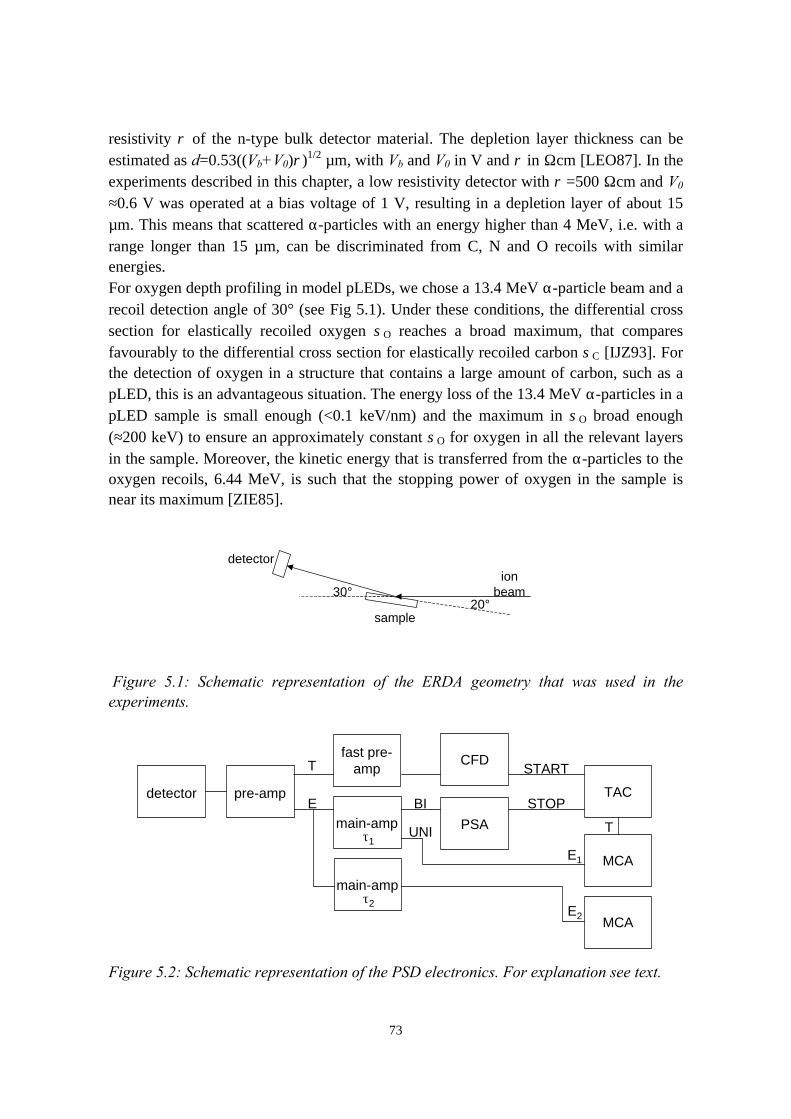
73
resistivity ρ of the n-type bulk detector material. The depletion layer thickness can beestimated as d=0.53((Vb+V0)ρ)1/2 µm, with Vb and V0 in V and ρ in Ωcm [LEO87]. In theexperiments described in this chapter, a low resistivity detector with ρ =500 Ωcm and V0
≈0.6 V was operated at a bias voltage of 1 V, resulting in a depletion layer of about 15µm. This means that scattered α-particles with an energy higher than 4 MeV, i.e. with arange longer than 15 µm, can be discriminated from C, N and O recoils with similarenergies.For oxygen depth profiling in model pLEDs, we chose a 13.4 MeV α-particle beam and arecoil detection angle of 30° (see Fig 5.1). Under these conditions, the differential crosssection for elastically recoiled oxygen σO reaches a broad maximum, that comparesfavourably to the differential cross section for elastically recoiled carbon σC [IJZ93]. Forthe detection of oxygen in a structure that contains a large amount of carbon, such as apLED, this is an advantageous situation. The energy loss of the 13.4 MeV α-particles in apLED sample is small enough (<0.1 keV/nm) and the maximum in σO broad enough(≈200 keV) to ensure an approximately constant σO for oxygen in all the relevant layersin the sample. Moreover, the kinetic energy that is transferred from the α-particles to theoxygen recoils, 6.44 MeV, is such that the stopping power of oxygen in the sample isnear its maximum [ZIE85].
sample
30°20°
ionbeam
detector
Figure 5.1: Schematic representation of the ERDA geometry that was used in theexperiments.
detector pre-amp
fast pre-amp
CFD
TAC
main-amp PSA
T
E BI
START
STOP
UNI
MCA
main-amp
MCA
T
E1
τ2
τ1
E2
Figure 5.2: Schematic representation of the PSD electronics. For explanation see text.
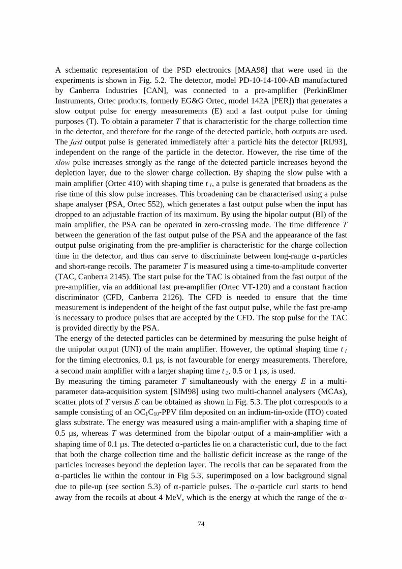
74
A schematic representation of the PSD electronics [MAA98] that were used in theexperiments is shown in Fig. 5.2. The detector, model PD-10-14-100-AB manufacturedby Canberra Industries [CAN], was connected to a pre-amplifier (PerkinElmerInstruments, Ortec products, formerly EG&G Ortec, model 142A [PER]) that generates aslow output pulse for energy measurements (E) and a fast output pulse for timingpurposes (T). To obtain a parameter T that is characteristic for the charge collection timein the detector, and therefore for the range of the detected particle, both outputs are used.The fast output pulse is generated immediately after a particle hits the detector [RIJ93],independent on the range of the particle in the detector. However, the rise time of theslow pulse increases strongly as the range of the detected particle increases beyond thedepletion layer, due to the slower charge collection. By shaping the slow pulse with amain amplifier (Ortec 410) with shaping time τ1, a pulse is generated that broadens as therise time of this slow pulse increases. This broadening can be characterised using a pulseshape analyser (PSA, Ortec 552), which generates a fast output pulse when the input hasdropped to an adjustable fraction of its maximum. By using the bipolar output (BI) of themain amplifier, the PSA can be operated in zero-crossing mode. The time difference Tbetween the generation of the fast output pulse of the PSA and the appearance of the fastoutput pulse originating from the pre-amplifier is characteristic for the charge collectiontime in the detector, and thus can serve to discriminate between long-range α-particlesand short-range recoils. The parameter T is measured using a time-to-amplitude converter(TAC, Canberra 2145). The start pulse for the TAC is obtained from the fast output of thepre-amplifier, via an additional fast pre-amplifier (Ortec VT-120) and a constant fractiondiscriminator (CFD, Canberra 2126). The CFD is needed to ensure that the timemeasurement is independent of the height of the fast output pulse, while the fast pre-ampis necessary to produce pulses that are accepted by the CFD. The stop pulse for the TACis provided directly by the PSA.The energy of the detected particles can be determined by measuring the pulse height ofthe unipolar output (UNI) of the main amplifier. However, the optimal shaping time τ1
for the timing electronics, 0.1 µs, is not favourable for energy measurements. Therefore,a second main amplifier with a larger shaping time τ2, 0.5 or 1 µs, is used.By measuring the timing parameter T simultaneously with the energy E in a multi-parameter data-acquisition system [SIM98] using two multi-channel analysers (MCAs),scatter plots of T versus E can be obtained as shown in Fig. 5.3. The plot corresponds to asample consisting of an OC1C10-PPV film deposited on an indium-tin-oxide (ITO) coatedglass substrate. The energy was measured using a main-amplifier with a shaping time of0.5 µs, whereas T was determined from the bipolar output of a main-amplifier with ashaping time of 0.1 µs. The detected α-particles lie on a characteristic curl, due to the factthat both the charge collection time and the ballistic deficit increase as the range of theparticles increases beyond the depletion layer. The recoils that can be separated from theα-particles lie within the contour in Fig 5.3, superimposed on a low background signaldue to pile-up (see section 5.3) of α-particle pulses. The α-particle curl starts to bendaway from the recoils at about 4 MeV, which is the energy at which the range of the α-
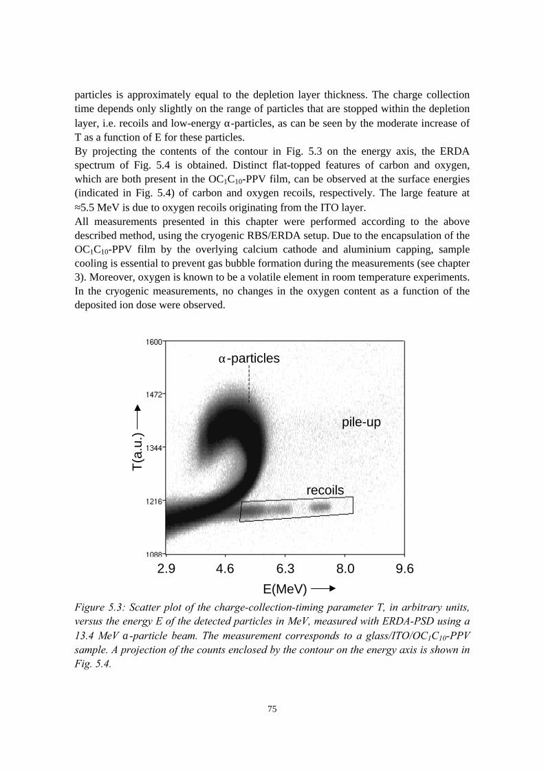
75
particles is approximately equal to the depletion layer thickness. The charge collectiontime depends only slightly on the range of particles that are stopped within the depletionlayer, i.e. recoils and low-energy α-particles, as can be seen by the moderate increase ofT as a function of E for these particles.By projecting the contents of the contour in Fig. 5.3 on the energy axis, the ERDAspectrum of Fig. 5.4 is obtained. Distinct flat-topped features of carbon and oxygen,which are both present in the OC1C10-PPV film, can be observed at the surface energies(indicated in Fig. 5.4) of carbon and oxygen recoils, respectively. The large feature at≈5.5 MeV is due to oxygen recoils originating from the ITO layer.All measurements presented in this chapter were performed according to the abovedescribed method, using the cryogenic RBS/ERDA setup. Due to the encapsulation of theOC1C10-PPV film by the overlying calcium cathode and aluminium capping, samplecooling is essential to prevent gas bubble formation during the measurements (see chapter3). Moreover, oxygen is known to be a volatile element in room temperature experiments.In the cryogenic measurements, no changes in the oxygen content as a function of thedeposited ion dose were observed.
E(MeV)
T(a
.u.)
recoils
α-particles
pile-up
2.9 9.68.06.34.6
Figure 5.3: Scatter plot of the charge-collection-timing parameter T, in arbitrary units,versus the energy E of the detected particles in MeV, measured with ERDA-PSD using a13.4 MeV α-particle beam. The measurement corresponds to a glass/ITO/OC1C10-PPVsample. A projection of the counts enclosed by the contour on the energy axis is shown inFig. 5.4.
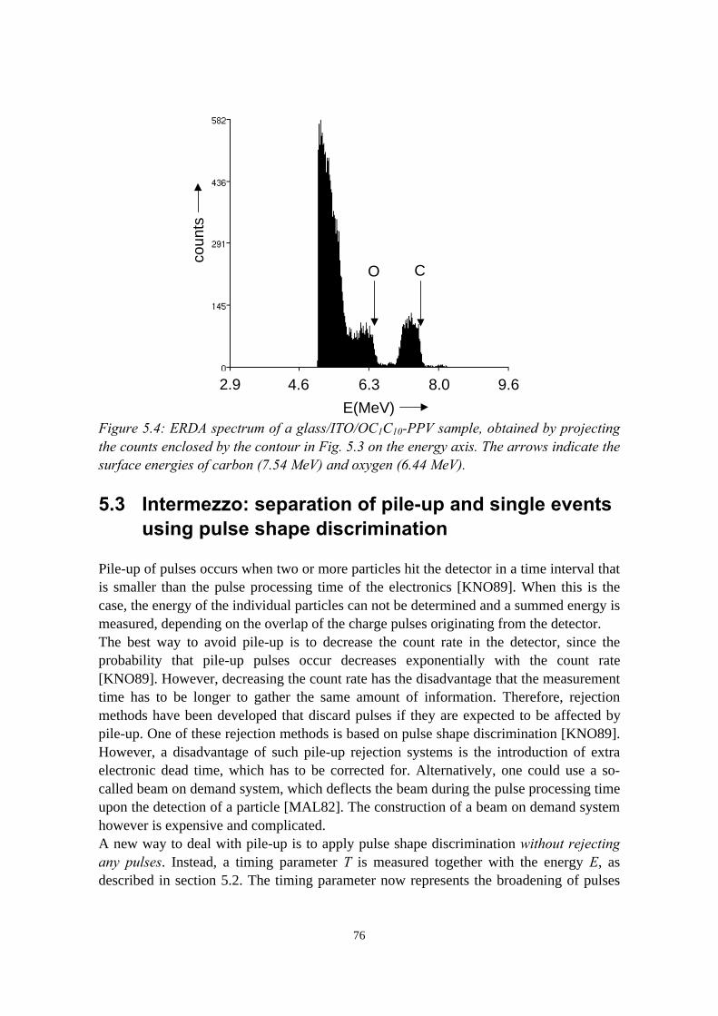
76
E(MeV)
2.9 9.68.06.34.6
coun
ts
CO
Figure 5.4: ERDA spectrum of a glass/ITO/OC1C10-PPV sample, obtained by projectingthe counts enclosed by the contour in Fig. 5.3 on the energy axis. The arrows indicate thesurface energies of carbon (7.54 MeV) and oxygen (6.44 MeV).
5.3 Intermezzo: separation of pile-up and single eventsusing pulse shape discrimination
Pile-up of pulses occurs when two or more particles hit the detector in a time interval thatis smaller than the pulse processing time of the electronics [KNO89]. When this is thecase, the energy of the individual particles can not be determined and a summed energy ismeasured, depending on the overlap of the charge pulses originating from the detector.The best way to avoid pile-up is to decrease the count rate in the detector, since theprobability that pile-up pulses occur decreases exponentially with the count rate[KNO89]. However, decreasing the count rate has the disadvantage that the measurementtime has to be longer to gather the same amount of information. Therefore, rejectionmethods have been developed that discard pulses if they are expected to be affected bypile-up. One of these rejection methods is based on pulse shape discrimination [KNO89].However, a disadvantage of such pile-up rejection systems is the introduction of extraelectronic dead time, which has to be corrected for. Alternatively, one could use a so-called beam on demand system, which deflects the beam during the pulse processing timeupon the detection of a particle [MAL82]. The construction of a beam on demand systemhowever is expensive and complicated.A new way to deal with pile-up is to apply pulse shape discrimination without rejectingany pulses. Instead, a timing parameter T is measured together with the energy E, asdescribed in section 5.2. The timing parameter now represents the broadening of pulses
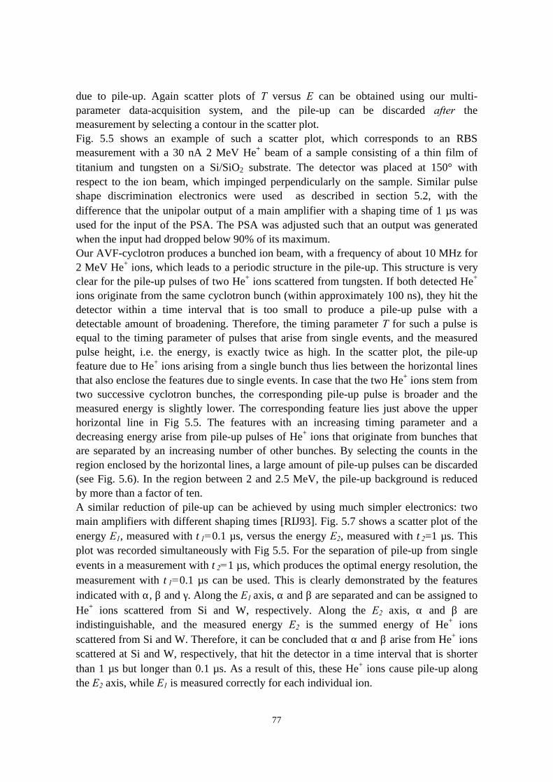
77
due to pile-up. Again scatter plots of T versus E can be obtained using our multi-parameter data-acquisition system, and the pile-up can be discarded after themeasurement by selecting a contour in the scatter plot.Fig. 5.5 shows an example of such a scatter plot, which corresponds to an RBSmeasurement with a 30 nA 2 MeV He+ beam of a sample consisting of a thin film oftitanium and tungsten on a Si/SiO2 substrate. The detector was placed at 150° withrespect to the ion beam, which impinged perpendicularly on the sample. Similar pulseshape discrimination electronics were used as described in section 5.2, with thedifference that the unipolar output of a main amplifier with a shaping time of 1 µs wasused for the input of the PSA. The PSA was adjusted such that an output was generatedwhen the input had dropped below 90% of its maximum.Our AVF-cyclotron produces a bunched ion beam, with a frequency of about 10 MHz for2 MeV He+ ions, which leads to a periodic structure in the pile-up. This structure is veryclear for the pile-up pulses of two He+ ions scattered from tungsten. If both detected He+
ions originate from the same cyclotron bunch (within approximately 100 ns), they hit thedetector within a time interval that is too small to produce a pile-up pulse with adetectable amount of broadening. Therefore, the timing parameter T for such a pulse isequal to the timing parameter of pulses that arise from single events, and the measuredpulse height, i.e. the energy, is exactly twice as high. In the scatter plot, the pile-upfeature due to He+ ions arising from a single bunch thus lies between the horizontal linesthat also enclose the features due to single events. In case that the two He+ ions stem fromtwo successive cyclotron bunches, the corresponding pile-up pulse is broader and themeasured energy is slightly lower. The corresponding feature lies just above the upperhorizontal line in Fig 5.5. The features with an increasing timing parameter and adecreasing energy arise from pile-up pulses of He+ ions that originate from bunches thatare separated by an increasing number of other bunches. By selecting the counts in theregion enclosed by the horizontal lines, a large amount of pile-up pulses can be discarded(see Fig. 5.6). In the region between 2 and 2.5 MeV, the pile-up background is reducedby more than a factor of ten.A similar reduction of pile-up can be achieved by using much simpler electronics: twomain amplifiers with different shaping times [RIJ93]. Fig. 5.7 shows a scatter plot of theenergy E1, measured with τ1=0.1 µs, versus the energy E2, measured with τ2=1 µs. Thisplot was recorded simultaneously with Fig 5.5. For the separation of pile-up from singleevents in a measurement with τ2=1 µs, which produces the optimal energy resolution, themeasurement with τ1=0.1 µs can be used. This is clearly demonstrated by the featuresindicated with α, β and γ. Along the E1 axis, α and β are separated and can be assigned toHe+ ions scattered from Si and W, respectively. Along the E2 axis, α and β areindistinguishable, and the measured energy E2 is the summed energy of He+ ionsscattered from Si and W. Therefore, it can be concluded that α and β arise from He+ ionsscattered at Si and W, respectively, that hit the detector in a time interval that is shorterthan 1 µs but longer than 0.1 µs. As a result of this, these He+ ions cause pile-up alongthe E2 axis, while E1 is measured correctly for each individual ion.
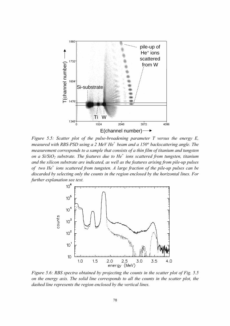
78
E(channel number)
T(c
hann
el n
umbe
r)
Si-substrate
pile-up ofHe+ ionsscatteredfrom W
Ti W
Figure 5.5: Scatter plot of the pulse-broadening parameter T versus the energy E,measured with RBS-PSD using a 2 MeV He+ beam and a 150° backscattering angle. Themeasurement corresponds to a sample that consists of a thin film of titanium and tungstenon a Si/SiO2 substrate. The features due to He+ ions scattered from tungsten, titaniumand the silicon substrate are indicated, as well as the features arising from pile-up pulsesof two He+ ions scattered from tungsten. A large fraction of the pile-up pulses can bediscarded by selecting only the counts in the region enclosed by the horizontal lines. Forfurther explanation see text.
Figure 5.6: RBS spectra obtained by projecting the counts in the scatter plot of Fig. 5.5on the energy axis. The solid line corresponds to all the counts in the scatter plot, thedashed line represents the region enclosed by the vertical lines.
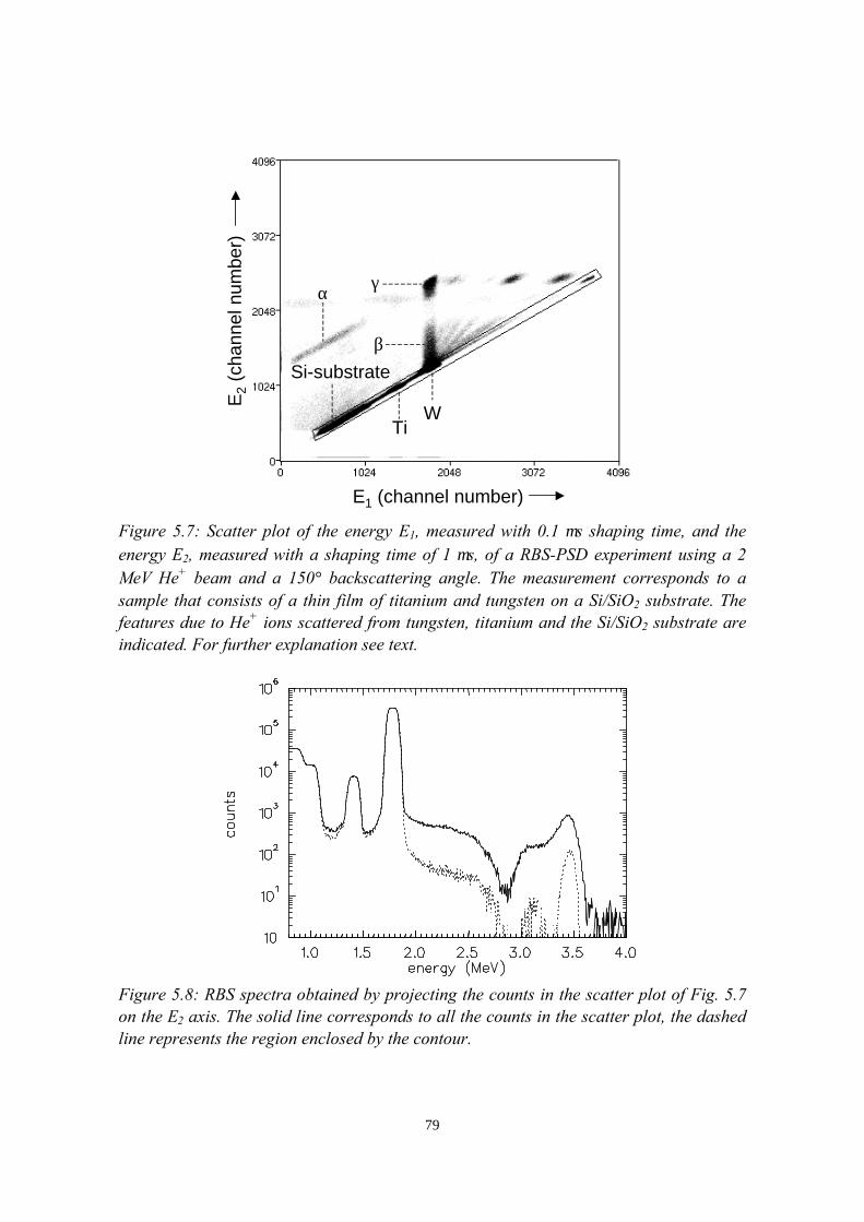
79
E1 (channel number)
E2 (
chan
nel n
umbe
r)
Si-substrate
TiW
α γ
β
Figure 5.7: Scatter plot of the energy E1, measured with 0.1 µs shaping time, and theenergy E2, measured with a shaping time of 1 µs, of a RBS-PSD experiment using a 2MeV He+ beam and a 150° backscattering angle. The measurement corresponds to asample that consists of a thin film of titanium and tungsten on a Si/SiO2 substrate. Thefeatures due to He+ ions scattered from tungsten, titanium and the Si/SiO2 substrate areindicated. For further explanation see text.
Figure 5.8: RBS spectra obtained by projecting the counts in the scatter plot of Fig. 5.7on the E2 axis. The solid line corresponds to all the counts in the scatter plot, the dashedline represents the region enclosed by the contour.
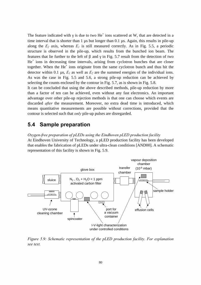
80
The feature indicated with γ is due to two He+ ions scattered at W, that are detected in atime interval that is shorter than 1 µs but longer than 0.1 µs. Again, this results in pile-upalong the E2 axis, whereas E1 is still measured correctly. As in Fig. 5.5, a periodicstructure is observed in the pile-up, which results from the bunched ion beam. Thefeatures that lie further to the left of β and γ in Fig. 5.7 result from the detection of twoHe+ ions in decreasing time intervals, arising from cyclotron bunches that are closertogether. When the He+ ions originate from the same cyclotron bunch and thus hit thedetector within 0.1 µs, E1 as well as E2 are the summed energies of the individual ions.As was the case in Fig. 5.5 and 5.6, a strong pile-up reduction can be achieved byselecting the counts enclosed by the contour in Fig. 5.7, as is shown in Fig. 5.8.It can be concluded that using the above described methods, pile-up reduction by morethan a factor of ten can be achieved, even without any fast electronics. An importantadvantage over other pile-up rejection methods is that one can choose which events arediscarded after the measurement. Moreover, no extra dead time is introduced, whichmeans quantitative measurements are possible without corrections, provided that thecontour is selected such that only pile-up pulses are disregarded.
5.4 Sample preparation
Oxygen-free preparation of pLEDs using the Eindhoven pLED production facilityAt Eindhoven University of Technology, a pLED production facility has been developedthat enables the fabrication of pLEDs under ultra-clean conditions [AND00]. A schematicrepresentation of this facility is shown in Fig. 5.9.
spincoater
UV-ozonecleaning chamber
sluice
port fora vacuumcontainer
transferchamber
vapour depositionchamber
(10-9 mbar)glove box
N2 , O2 + H2O < 1 ppmactivated carbon filter
effusion cells
sample holder
I-V-light characterizationunder controlled conditions
Figure 5.9: Schematic representation of the pLED production facility. For explanationsee text.
81
The pLED production facility is constructed such that all production steps can be carriedout under well defined conditions, either in a nitrogen atmosphere or in vacuum, withoutany exposure to air. Moreover, the glove box is equipped with a port that accepts theportable vacuum container of the cryogenic RBS/ERDA setup (see chapter 2). Thisenables the transport of pLEDs in a nitrogen atmosphere.After wet cleaning in ultrasonic baths of acetone and 2-propanol, ITO-coated glasssubstrates [MER] were introduced into the UV-ozone cleaning chamber [VIG85].Initially, this chamber was filled with air, from which reactive ozone was formed by UV-light. After a 20 minutes UV-ozone treatment, by which hydrocarbons were effectivelyremoved from the substrates, the chamber was evacuated and subsequently filled withnitrogen. The cleaned glass/ITO substrates were then transferred to the glove box, wherean OC1C10-PPV film was deposited by spin coating from a 1 wt.% solution in toluene.After depositing the OC1C10-PPV film, the semimanufactured pLEDs were introducedinto the vapour deposition chamber via the transfer chamber. In the vapour depositionchamber, with a base pressure of 10-9 mbar, calcium cathodes and aluminium cappinglayers were deposited by evaporation from effusion cells. The thickness of the depositedlayers was determined using quartz crystal monitors. Directly after depositing the calciumcathode and the aluminium capping, in-situ I-V-light characterisation of the pLEDs wasperformed inside the evaporation chamber, using an in-house build setup.Crucial for the ERDA experiments was the transfer of the pLED samples from theproduction facility to the cryogenic RBS/ERDA setup. This was carried out in a drynitrogen environment, using a portable vacuum container (see chapter 2). Transportthrough air would destroy the samples, due to the extreme oxidation sensitivity of thecalcium cathode.
Post-deposition oxidation of thin Ca films with dry oxygenTo study the effect of the exposure of pLEDs with a calcium cathode to oxygen, thefollowing procedure was carried out. The deposition of the calcium cathodes wasinterrupted after a certain amount of calcium had been deposited, and the so-producedsemimanufactured pLEDs were exposed to dry oxygen in the transfer chamber (basepressure 5*10-8 mbar). The thickness of the calcium layer was varied between 0 and 80nm in five steps: 5, 10, 20, 40 and 80 nm. The exposure time ranged from 0.5 to 20minutes, and the oxygen pressure in the transfer chamber was varied between 30 and1000 mbar. After exposing the semimanufactured pLEDs to oxygen, the deposition of thecalcium cathode was continued in the evaporation chamber, such that a total thickness of80 nm calcium was deposited. The pLEDs were completed by depositing a 40 nmaluminium capping.
Ca oxidation during depositionThe significance of the presence of residual oxygen gas in the evaporation chamber wasinvestigated as follows. During deposition of the calcium cathodes, the oxygenbackground pressure was controlled by admitting oxygen gas in the evaporation chamber
82
through a variable leak valve. Using a quadrupole mass spectrometer, the oxygenbackground pressure was adjusted as 10-8, 10-7, 10-6 and 10-5 mbar.
5.5 Electrical and compositional characterisation of thepLEDs
5.5.1 pLEDs without oxidation of the Ca cathode
Without any oxidation of the Ca cathode, high brightness (≈4⋅102 Cd/m2 at 5 V) pLEDswere obtained, with a reproducibility of the current-density/brightness versus voltagecurves within 15%. The efficiency of the pLEDs at 5 V operating voltage was ≈0.5 Cd/A.A plot of the current density and the brightness as a function of the applied voltagecorresponding to a typical oxygen-free prepared device, measured in the UHV chamber,is shown in Fig. 5.10.Using ERDA-PSD (see section 5.2), the amount of oxygen in the various layers of thepLEDs was measured. Simulations of the ERDA spectra were performed using amodified version of the RUMP code [SIG, JAE94]. The differential cross sections forelastic scattering of 13.4 MeV α particles at carbon and oxygen were taken fromreferences [MEH67] and [MIT64], respectively. The cross sections reported in thesereferences were measured at slightly different recoil angles than the 30° detection anglethat was used in the experiments. Corrections for the deviations were made using theangle dependent cross section measurements published in reference [IJZ93]. In RUMP,the stopping powers of carbon and oxygen recoils are calculated according to reference[ZIE85].Fig. 5.11 shows an ERDA spectrum of a glass/ITO/OC1C10-PPV reference sample. In theRUMP simulation, the composition of the 150 nm thick OC1C10-PPV film was assumedto be 19% C, 57% H and 4% O. Distinct flat-topped features can be seen, that correspondto carbon and oxygen recoils arising from the OC1C10-PPV film. The counts that appearabove the surface energy of carbon and in between the carbon and oxygen features aredue to pile-up pulses of scattered α particles (see section 5.2). The large feature below5.5 MeV is due to oxygen in the ITO layer.Fig. 5.12 shows the ERDA spectrum of a pLED consisting of a glass/ITO substrate, a 130nm OC1C10-PPV film, a 80 nm calcium cathode and a 40 nm aluminium capping. Apartfrom the features that are due to carbon and oxygen in the OC1C10-PPV film, two otherpeaks can be seen. The peak located at the surface energy of oxygen recoils, 6.44 MeV, isdue to oxidation of the aluminium capping during storage in the glove box. Simulationsof the spectrum showed that an oxygen areal density of 9⋅1015 at./cm2 was present at thesurface, which corresponds to a stoichiometric aluminium oxide (Al2O3) of 6 nm.
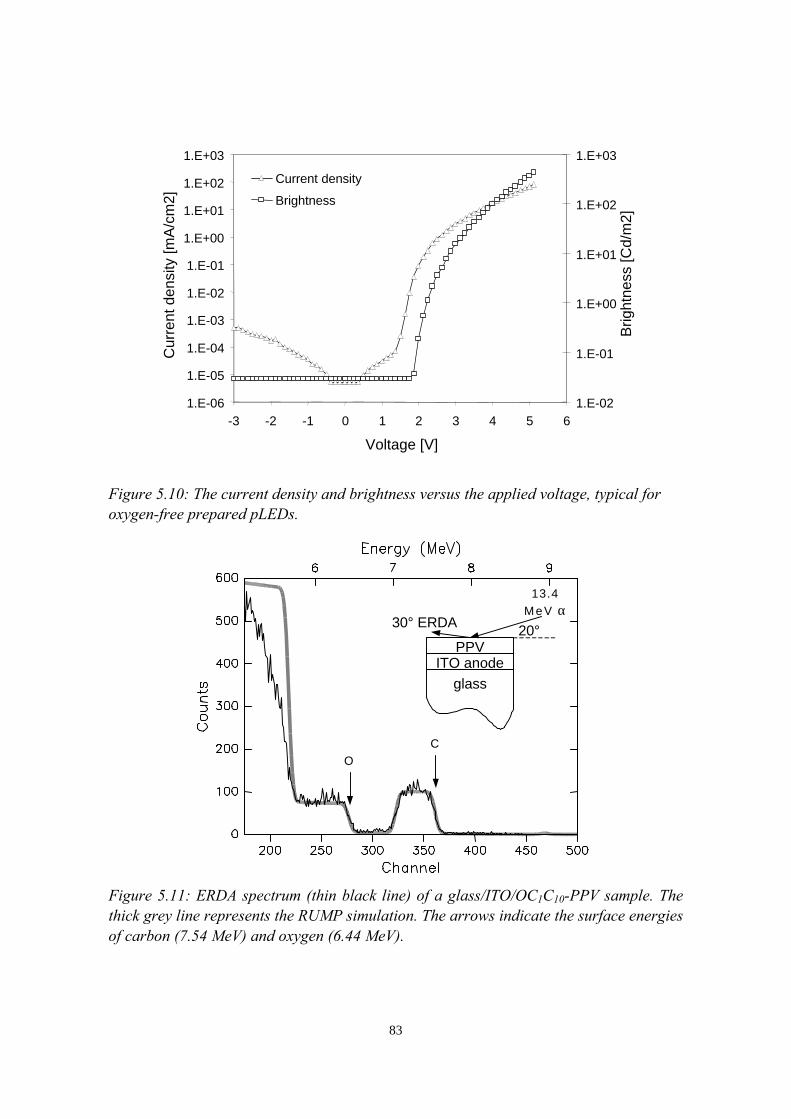
83
1.E-06
1.E-05
1.E-04
1.E-03
1.E-02
1.E-01
1.E+00
1.E+01
1.E+02
1.E+03
-3 -2 -1 0 1 2 3 4 5 6
Voltage [V]
Cur
rent
den
sity
[mA
/cm
2]
1.E-02
1.E-01
1.E+00
1.E+01
1.E+02
1.E+03
Brig
htne
ss [C
d/m
2]
Current density
Brightness
Figure 5.10: The current density and brightness versus the applied voltage, typical foroxygen-free prepared pLEDs.
C
O
13.4
MeV α30° ERDA
PPV
glass
ITO anode
20°
Figure 5.11: ERDA spectrum (thin black line) of a glass/ITO/OC1C10-PPV sample. Thethick grey line represents the RUMP simulation. The arrows indicate the surface energiesof carbon (7.54 MeV) and oxygen (6.44 MeV).
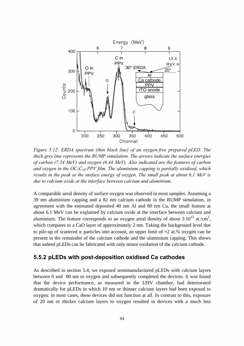
84
C
O
13.4
MeV α30° ERDA
ITO anodePPV
glass
20°Al
Ca cathode
C inPPV
O inPPV
Figure 5.12: ERDA spectrum (thin black line) of an oxygen-free prepared pLED. Thethick grey line represents the RUMP simulation. The arrows indicate the surface energiesof carbon (7.54 MeV) and oxygen (6.44 MeV). Also indicated are the features of carbonand oxygen in the OC1C10-PPV film. The aluminium capping is partially oxidised, whichresults in the peak at the surface energy of oxygen. The small peak at about 6.1 MeV isdue to calcium oxide at the interface between calcium and aluminium.
A comparable areal density of surface oxygen was observed in most samples. Assuming a39 nm aluminium capping and a 82 nm calcium cathode in the RUMP simulation, inagreement with the estimated deposited 40 nm Al and 80 nm Ca, the small feature atabout 6.1 MeV can be explained by calcium oxide at the interface between calcium andaluminium. The feature corresponds to an oxygen areal density of about 3⋅1015 at./cm2,which compares to a CaO layer of approximately 2 nm. Taking the background level dueto pile-up of scattered α particles into account, an upper limit of ≈2 at.% oxygen can bepresent in the remainder of the calcium cathode and the aluminium capping. This showsthat indeed pLEDs can be fabricated with only minor oxidation of the calcium cathode.
5.5.2 pLEDs with post-deposition oxidised Ca cathodes
As described in section 5.4, we exposed semimanufactured pLEDs with calcium layersbetween 0 and 80 nm to oxygen and subsequently completed the devices. It was foundthat the device performance, as measured in the UHV chamber, had deteriorateddramatically for pLEDs in which 10 nm or thinner calcium layers had been exposed tooxygen: in most cases, these devices did not function at all. In contrast to this, exposureof 20 nm or thicker calcium layers to oxygen resulted in devices with a much less
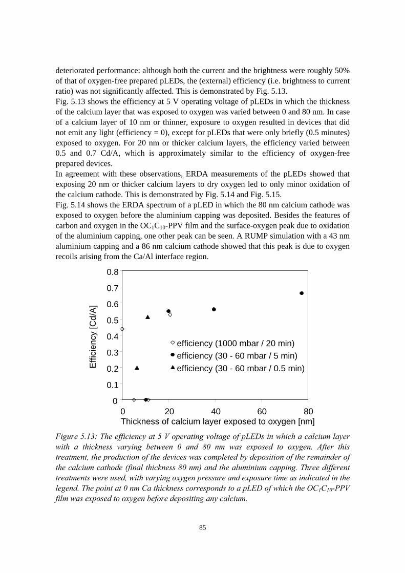
85
deteriorated performance: although both the current and the brightness were roughly 50%of that of oxygen-free prepared pLEDs, the (external) efficiency (i.e. brightness to currentratio) was not significantly affected. This is demonstrated by Fig. 5.13.Fig. 5.13 shows the efficiency at 5 V operating voltage of pLEDs in which the thicknessof the calcium layer that was exposed to oxygen was varied between 0 and 80 nm. In caseof a calcium layer of 10 nm or thinner, exposure to oxygen resulted in devices that didnot emit any light (efficiency = 0), except for pLEDs that were only briefly (0.5 minutes)exposed to oxygen. For 20 nm or thicker calcium layers, the efficiency varied between0.5 and 0.7 Cd/A, which is approximately similar to the efficiency of oxygen-freeprepared devices.In agreement with these observations, ERDA measurements of the pLEDs showed thatexposing 20 nm or thicker calcium layers to dry oxygen led to only minor oxidation ofthe calcium cathode. This is demonstrated by Fig. 5.14 and Fig. 5.15.Fig. 5.14 shows the ERDA spectrum of a pLED in which the 80 nm calcium cathode wasexposed to oxygen before the aluminium capping was deposited. Besides the features ofcarbon and oxygen in the OC1C10-PPV film and the surface-oxygen peak due to oxidationof the aluminium capping, one other peak can be seen. A RUMP simulation with a 43 nmaluminium capping and a 86 nm calcium cathode showed that this peak is due to oxygenrecoils arising from the Ca/Al interface region.
0
0.1
0.2
0.3
0.4
0.5
0.6
0.7
0.8
0 20 40 60 80Thickness of calcium layer exposed to oxygen [nm]
Effi
cien
cy [C
d/A
]
efficiency (1000 mbar / 20 min)
efficiency (30 - 60 mbar / 5 min)
efficiency (30 - 60 mbar / 0.5 min)
Figure 5.13: The efficiency at 5 V operating voltage of pLEDs in which a calcium layerwith a thickness varying between 0 and 80 nm was exposed to oxygen. After thistreatment, the production of the devices was completed by deposition of the remainder ofthe calcium cathode (final thickness 80 nm) and the aluminium capping. Three differenttreatments were used, with varying oxygen pressure and exposure time as indicated in thelegend. The point at 0 nm Ca thickness corresponds to a pLED of which the OC1C10-PPVfilm was exposed to oxygen before depositing any calcium.
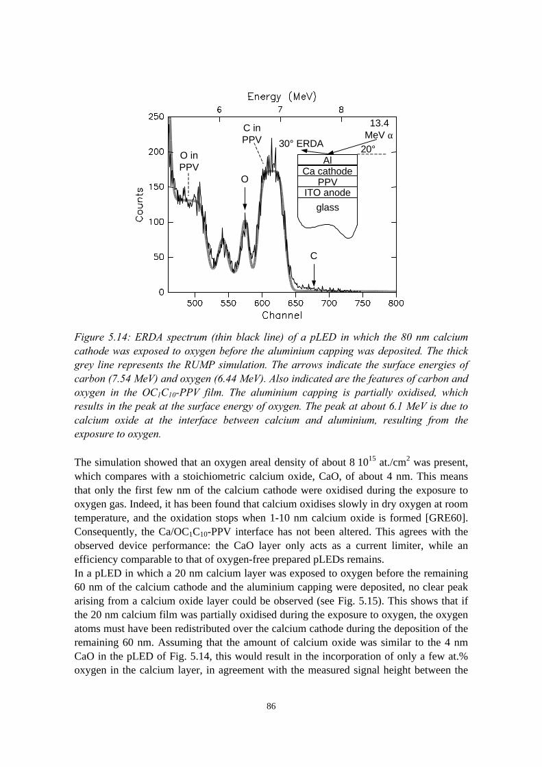
86
C
O
13.4MeV α
30° ERDA
ITO anodePPV
glass
20°Al
Ca cathode
C inPPV
O inPPV
Figure 5.14: ERDA spectrum (thin black line) of a pLED in which the 80 nm calciumcathode was exposed to oxygen before the aluminium capping was deposited. The thickgrey line represents the RUMP simulation. The arrows indicate the surface energies ofcarbon (7.54 MeV) and oxygen (6.44 MeV). Also indicated are the features of carbon andoxygen in the OC1C10-PPV film. The aluminium capping is partially oxidised, whichresults in the peak at the surface energy of oxygen. The peak at about 6.1 MeV is due tocalcium oxide at the interface between calcium and aluminium, resulting from theexposure to oxygen.
The simulation showed that an oxygen areal density of about 8⋅1015 at./cm2 was present,which compares with a stoichiometric calcium oxide, CaO, of about 4 nm. This meansthat only the first few nm of the calcium cathode were oxidised during the exposure tooxygen gas. Indeed, it has been found that calcium oxidises slowly in dry oxygen at roomtemperature, and the oxidation stops when 1-10 nm calcium oxide is formed [GRE60].Consequently, the Ca/OC1C10-PPV interface has not been altered. This agrees with theobserved device performance: the CaO layer only acts as a current limiter, while anefficiency comparable to that of oxygen-free prepared pLEDs remains.In a pLED in which a 20 nm calcium layer was exposed to oxygen before the remaining60 nm of the calcium cathode and the aluminium capping were deposited, no clear peakarising from a calcium oxide layer could be observed (see Fig. 5.15). This shows that ifthe 20 nm calcium film was partially oxidised during the exposure to oxygen, the oxygenatoms must have been redistributed over the calcium cathode during the deposition of theremaining 60 nm. Assuming that the amount of calcium oxide was similar to the 4 nmCaO in the pLED of Fig. 5.14, this would result in the incorporation of only a few at.%oxygen in the calcium layer, in agreement with the measured signal height between the
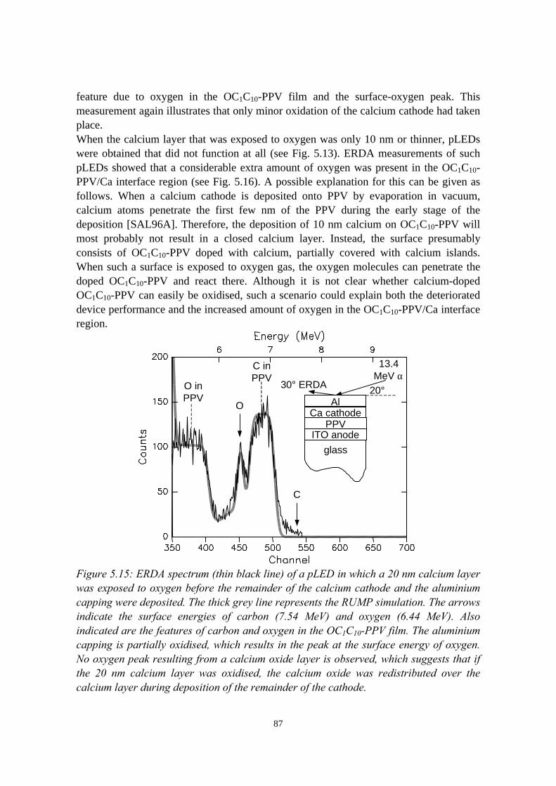
87
feature due to oxygen in the OC1C10-PPV film and the surface-oxygen peak. Thismeasurement again illustrates that only minor oxidation of the calcium cathode had takenplace.When the calcium layer that was exposed to oxygen was only 10 nm or thinner, pLEDswere obtained that did not function at all (see Fig. 5.13). ERDA measurements of suchpLEDs showed that a considerable extra amount of oxygen was present in the OC1C10-PPV/Ca interface region (see Fig. 5.16). A possible explanation for this can be given asfollows. When a calcium cathode is deposited onto PPV by evaporation in vacuum,calcium atoms penetrate the first few nm of the PPV during the early stage of thedeposition [SAL96A]. Therefore, the deposition of 10 nm calcium on OC1C10-PPV willmost probably not result in a closed calcium layer. Instead, the surface presumablyconsists of OC1C10-PPV doped with calcium, partially covered with calcium islands.When such a surface is exposed to oxygen gas, the oxygen molecules can penetrate thedoped OC1C10-PPV and react there. Although it is not clear whether calcium-dopedOC1C10-PPV can easily be oxidised, such a scenario could explain both the deteriorateddevice performance and the increased amount of oxygen in the OC1C10-PPV/Ca interfaceregion.
C
O
C inPPV
O inPPV
13.4MeV α
30° ERDA
ITO anodePPV
glass
20°Al
Ca cathode
Figure 5.15: ERDA spectrum (thin black line) of a pLED in which a 20 nm calcium layerwas exposed to oxygen before the remainder of the calcium cathode and the aluminiumcapping were deposited. The thick grey line represents the RUMP simulation. The arrowsindicate the surface energies of carbon (7.54 MeV) and oxygen (6.44 MeV). Alsoindicated are the features of carbon and oxygen in the OC1C10-PPV film. The aluminiumcapping is partially oxidised, which results in the peak at the surface energy of oxygen.No oxygen peak resulting from a calcium oxide layer is observed, which suggests that ifthe 20 nm calcium layer was oxidised, the calcium oxide was redistributed over thecalcium layer during deposition of the remainder of the cathode.
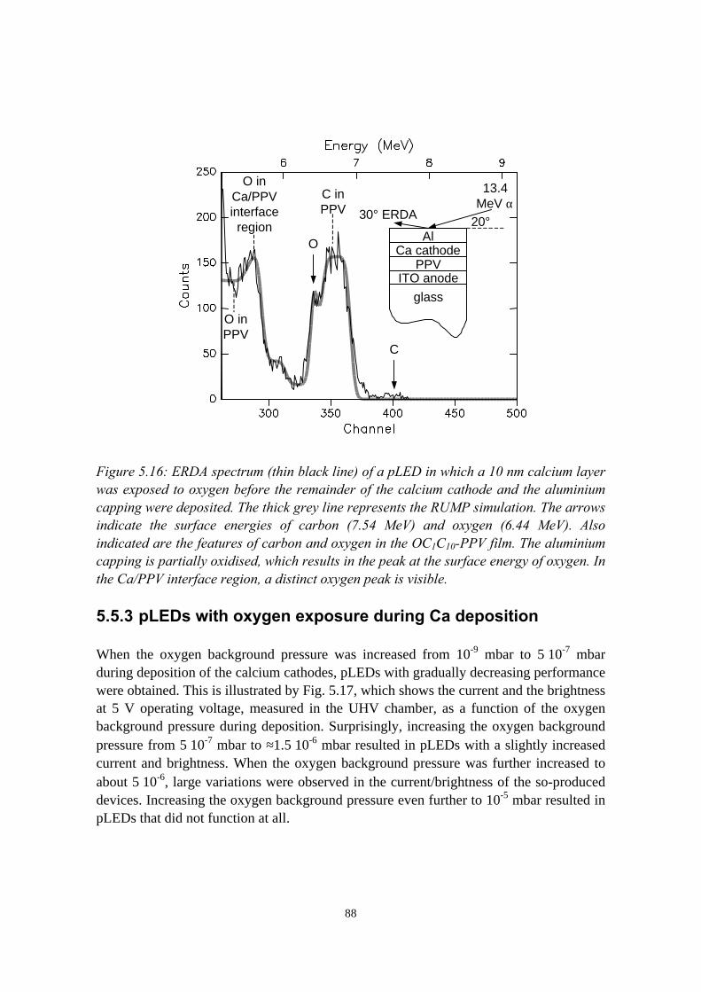
88
C
O
C inPPV
O inPPV
13.4MeV α
30° ERDA
ITO anodePPV
glass
20°Al
Ca cathode
O inCa/PPVinterfaceregion
Figure 5.16: ERDA spectrum (thin black line) of a pLED in which a 10 nm calcium layerwas exposed to oxygen before the remainder of the calcium cathode and the aluminiumcapping were deposited. The thick grey line represents the RUMP simulation. The arrowsindicate the surface energies of carbon (7.54 MeV) and oxygen (6.44 MeV). Alsoindicated are the features of carbon and oxygen in the OC1C10-PPV film. The aluminiumcapping is partially oxidised, which results in the peak at the surface energy of oxygen. Inthe Ca/PPV interface region, a distinct oxygen peak is visible.
5.5.3 pLEDs with oxygen exposure during Ca deposition
When the oxygen background pressure was increased from 10-9 mbar to 5⋅10-7 mbarduring deposition of the calcium cathodes, pLEDs with gradually decreasing performancewere obtained. This is illustrated by Fig. 5.17, which shows the current and the brightnessat 5 V operating voltage, measured in the UHV chamber, as a function of the oxygenbackground pressure during deposition. Surprisingly, increasing the oxygen backgroundpressure from 5⋅10-7 mbar to ≈1.5⋅10-6 mbar resulted in pLEDs with a slightly increasedcurrent and brightness. When the oxygen background pressure was further increased toabout 5⋅10-6, large variations were observed in the current/brightness of the so-produceddevices. Increasing the oxygen background pressure even further to 10-5 mbar resulted inpLEDs that did not function at all.

89
0
10
20
30
40
50
60
70
1E-09 1E-08 1E-07 1E-06 1E-05
oxygen pressure [mbar]
curr
ent [
mA
/cm
2]
0
50
100
150
200
250
300
350
400
brig
htne
ss [C
d/m
2]
currentbrightness
Figure 5.17: The current and brightness at 5 V operating voltage as a function of theoxygen background pressure in which the calcium cathode was deposited. The datapoints with the error bars each correspond to batches of six pLEDs, of which the calciumcathodes were deposited simultaneously. The error bars indicate the spread in thecurrent and brightness of the individual pLEDs. For an oxygen background pressure of5⋅10-6 mbar, an unusually large spread was observed in the current and brightness of thepLEDs, as can be seen from the data points that correspond to two of these pLEDs.Depositing the calcium cathodes in 10-5 mbar oxygen led to device failure.
ERDA measurements of the pLEDs showed that increasing the oxygen backgroundpressure from 10-9 mbar to 10-5 mbar during Ca deposition led to a gradually increasingincorporation of oxygen in the calcium cathode. In case of a 10-8 mbar oxygenbackground pressure, the amount of oxygen in the calcium cathode as determined byERDA was similar as in reference pLEDs, i.e. ≤ 2 at.% (see Fig. 5.18A). When theoxygen background pressure was increased to 10-7 mbar, a clear increase in the oxygenconcentration in the cathode was observed (see Fig. 5.18B). Simulations of the spectrumin Fig. 5.18B showed that the oxygen areal density in the calcium cathode was ≈1.5⋅1016
at./cm2. Since 80 nm calcium was deposited, this corresponds to a concentration of about10 at.%.It should be noted that the signal that extends to the right of the carbon features in Fig.18A and Fig. 18B is due to pile-up of α-particle pulses. Since the ERDA spectra in Fig.18 were obtained by projecting the counts within a selected contour in a scatter plot asshown in Fig. 5.3 on the energy axis, the background due to piled-up α-particle pulses iscut off at an energy that depends on the borders of the contour. In Fig. 18A, the cut-offenergy is coincidentally about equal to the surface energy of carbon recoils. The signalbetween the carbon feature, arising from the OC1C10-PPV film, and the carbon surfaceenergy is nevertheless due to piled-up α-particle pulses, and should not be misinterpretedas carbon recoils originating from the calcium and aluminium layers.
90
CO
13.4MeV α
30° ERDA
ITO anodePPV
glass
20°Al
Ca cathode
C inPPV
O inPPV
A
AlCa
CO
13.4MeV α
30° ERDA
ITO anodePPV
glass
20°Al
Ca cathode
C inPPV
O inCa
B
AlCa
Figure 5.18: ERDA spectra (thin black lines) of pLEDs in which the calcium cathodeswere deposited in a oxygen background pressure of 10-8 (A) and 10-7 (B) mbar,respectively. The thick grey lines represent the RUMP simulations. The arrows indicatethe surface energies of carbon (7.54 MeV) and oxygen (6.44 MeV). In B, a clear step dueto oxygen in the calcium cathode can be seen. The small peak at about 5.9 MeV in A isdue to calcium oxide at the Ca/Al interface. For clarity, a depth-scale for oxygen recoilsis shown in the upper left corners.
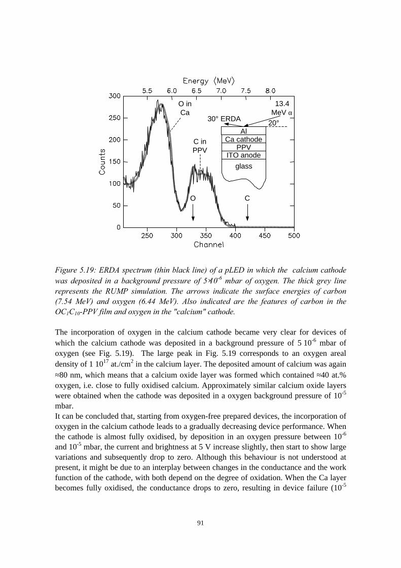
91
O inCa
CO
13.4MeV α
30° ERDA
ITO anodePPV
glass
20°Al
Ca cathodeC inPPV
Figure 5.19: ERDA spectrum (thin black line) of a pLED in which the calcium cathodewas deposited in a background pressure of 5⋅10-6 mbar of oxygen. The thick grey linerepresents the RUMP simulation. The arrows indicate the surface energies of carbon(7.54 MeV) and oxygen (6.44 MeV). Also indicated are the features of carbon in theOC1C10-PPV film and oxygen in the "calcium" cathode.
The incorporation of oxygen in the calcium cathode became very clear for devices ofwhich the calcium cathode was deposited in a background pressure of 5⋅10-6 mbar ofoxygen (see Fig. 5.19). The large peak in Fig. 5.19 corresponds to an oxygen arealdensity of 1⋅1017 at./cm2 in the calcium layer. The deposited amount of calcium was again≈80 nm, which means that a calcium oxide layer was formed which contained ≈40 at.%oxygen, i.e. close to fully oxidised calcium. Approximately similar calcium oxide layerswere obtained when the cathode was deposited in a oxygen background pressure of 10-5
mbar.It can be concluded that, starting from oxygen-free prepared devices, the incorporation ofoxygen in the calcium cathode leads to a gradually decreasing device performance. Whenthe cathode is almost fully oxidised, by deposition in an oxygen pressure between 10-6
and 10-5 mbar, the current and brightness at 5 V increase slightly, then start to show largevariations and subsequently drop to zero. Although this behaviour is not understood atpresent, it might be due to an interplay between changes in the conductance and the workfunction of the cathode, with both depend on the degree of oxidation. When the Ca layerbecomes fully oxidised, the conductance drops to zero, resulting in device failure (10-5
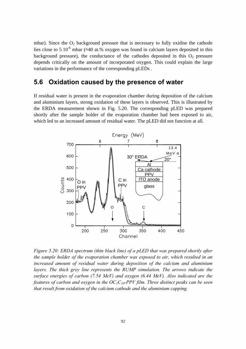
92
mbar). Since the O2 background pressure that is necessary to fully oxidise the cathodelies close to 5⋅10-6 mbar (≈40 at.% oxygen was found in calcium layers deposited in thisbackground pressure), the conductance of the cathodes deposited in this O2 pressuredepends critically on the amount of incorporated oxygen. This could explain the largevariations in the performance of the corresponding pLEDs .
5.6 Oxidation caused by the presence of water
If residual water is present in the evaporation chamber during deposition of the calciumand aluminium layers, strong oxidation of these layers is observed. This is illustrated bythe ERDA measurement shown in Fig. 5.20. The corresponding pLED was preparedshortly after the sample holder of the evaporation chamber had been exposed to air,which led to an increased amount of residual water. The pLED did not function at all.
CO
13.4
M e V α30° ERDA
ITO anodePPV
glass
20°Al
Ca cathode
C inPPV
O inPPV
Figure 5.20: ERDA spectrum (thin black line) of a pLED that was prepared shortly afterthe sample holder of the evaporation chamber was exposed to air, which resulted in anincreased amount of residual water during deposition of the calcium and aluminiumlayers. The thick grey line represents the RUMP simulation. The arrows indicate thesurface energies of carbon (7.54 MeV) and oxygen (6.44 MeV). Also indicated are thefeatures of carbon and oxygen in the OC1C10-PPV film. Three distinct peaks can be seenthat result from oxidation of the calcium cathode and the aluminium capping.
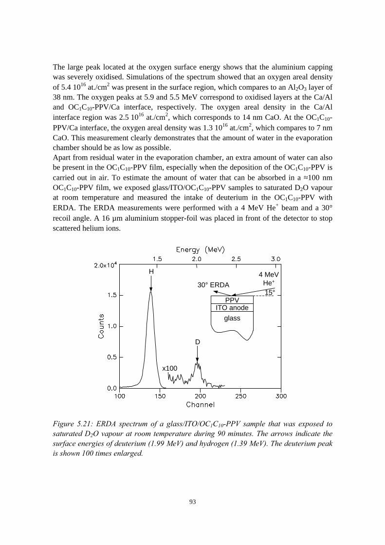
93
The large peak located at the oxygen surface energy shows that the aluminium cappingwas severely oxidised. Simulations of the spectrum showed that an oxygen areal densityof 5.4⋅1016 at./cm2 was present in the surface region, which compares to an Al2O3 layer of38 nm. The oxygen peaks at 5.9 and 5.5 MeV correspond to oxidised layers at the Ca/Aland OC1C10-PPV/Ca interface, respectively. The oxygen areal density in the Ca/Alinterface region was 2.5⋅1016 at./cm2, which corresponds to 14 nm CaO. At the OC1C10-PPV/Ca interface, the oxygen areal density was 1.3⋅1016 at./cm2, which compares to 7 nmCaO. This measurement clearly demonstrates that the amount of water in the evaporationchamber should be as low as possible.Apart from residual water in the evaporation chamber, an extra amount of water can alsobe present in the OC1C10-PPV film, especially when the deposition of the OC1C10-PPV iscarried out in air. To estimate the amount of water that can be absorbed in a ≈100 nmOC1C10-PPV film, we exposed glass/ITO/OC1C10-PPV samples to saturated D2O vapourat room temperature and measured the intake of deuterium in the OC1C10-PPV withERDA. The ERDA measurements were performed with a 4 MeV He+ beam and a 30°recoil angle. A 16 µm aluminium stopper-foil was placed in front of the detector to stopscattered helium ions.
4 MeVHe+
30° ERDA
ITO anodePPV
glass
15°
D
H
x100
Figure 5.21: ERDA spectrum of a glass/ITO/OC1C10-PPV sample that was exposed tosaturated D2O vapour at room temperature during 90 minutes. The arrows indicate thesurface energies of deuterium (1.99 MeV) and hydrogen (1.39 MeV). The deuterium peakis shown 100 times enlarged.
94
Fig. 5.21 shows an ERDA spectrum of a glass/ITO/OC1C10-PPV sample that wasexposed to D2O for 90 minutes at room temperature. Directly after this treatment, whichwas carried out in the load lock of the setup, the sample was transferred to the analysischamber. This situation thus closely resembles that of a water-containingsemimanufactured pLED that has been introduced in a evaporation chamber for thedeposition of the cathode. Analysis of the spectrum showed that ≈7⋅1014 at./cm2
deuterium was present in the OC1C10-PPV film, i.e. about 4⋅1014 D2O molecules/cm2. Fora 100 nm OC1C10-PPV film, this compares to a deuterated water concentration of theorder of 0.1 wt.%. In a similar sample that was annealed for 20 hours at 200 °C invacuum after being exposed to D2O, no detectable amount of deuterium was present. Thisdemonstrates that water can be removed from an OC1C10-PPV film by means of anannealing step.
5.7 Conclusions
Oxygen-free fabrication of pLEDs in our pLED production facility resulted in high-performance devices, with a light output of ≈4⋅102 Cd/m2 at 5 V, that could be made withgood reproducibility.Post-deposition oxidation with dry oxygen of 20 nm or thicker calcium films insemimanufactured pLEDs resulted in roughly 50% loss of current and brightness at 5 Voperating voltage, without significantly affecting the efficiency. In agreement with theseobservations, ERDA measurements showed that in such pLEDs the calcium cathode wasslightly oxidised, while the OC1C10-PPV/Ca interface was not affected. A similaroxidation treatment of 10 nm or thinner calcium layers resulted in a dramaticdeterioration of the devices, which could be related with the incorporation of oxygen inthe OC1C10-PPV/Ca interface region. Most probably the deposition of 10 nm calcium didnot result in the formation of a closed calcium layer, which would give oxygen access tothe OC1C10-PPV, of which the surface region is known to be doped with Ca2+ ions[SAL96A]. Oxidation of this doped surface region seems a likely explanation for both thedeteriorated device performance and the presence of additional oxygen in the OC1C10-PPV/Ca interface region.Deposition of the calcium cathode in an oxygen background pressure resulted in devicesof which the performance deteriorated gradually as the background pressure wasincreased from 10-9 to <10-6 mbar. Slightly above 10-6 mbar, the current and brightnessshowed a local maximum, followed by a strong variation in the device performance at5⋅10-6 mbar and device failure at 10-5 mbar. ERDA measurements showed that increasingthe oxygen background pressure resulted in the incorporation of an increasing amount ofoxygen in the calcium cathode. For oxygen pressures between 10-6 and 10-5 mbar, i.e. inthe range where strong variations are observed in the device performance, the calciumcathode proved to be almost fully oxidised. The trend in the device performance is notunderstood at present, but might be explained by an interplay between variations in theconductance and the work function of the cathode.

95
If residual water is present in the vapour deposition chamber, strong oxidation of themetal layers occurs that leads to device failure. ERDA measurements of OC1C10-PPVfilms that had been exposed to D2O have pointed out that OC1C10-PPV can contain about0.1 wt.% water. This demonstrates that care should be taken that not only the depositionchamber is free of water, but also the OC1C10-PPV film.
References
[AMS60] G. Amsel, P. Baruch, O. Smulkowski, Nucl. Instr. and Meth. 8 (1960) 92[AND00] G.G. Andersson, M.P. de Jong, H.H. Brongersma, A.W. Denier van der
Gon, L.J. van IJzendoorn, M.J.A. de Voigt, to be published in Synth. Met.[BRO95] P. Bröms, J. Birgersson, N. Johnsson, M. Lögdlund, W.R. Salaneck,
Synth. Met. 74 (1995) 179[CAN] Canberra Industries (www.canberra.com), Meriden, CT 06450, USA[GAO92] Y. Gao, K.T. Park, B.R. Hsieh, J. Chem. Phys. 97 (1992) 6991[GRE60] S.J. Gregg, W.B. Jepson, J. chem. Soc. (1960) 712[IJZ93] L.J. van IJzendoorn, H.A. Rijken, S.S. Klein, M.J.A. de Voigt, Appl. Surf.
Sci. 70/71 (1993) 58[JAE94] L. Jaegers, Elastic recoil detection analysis with He ions, (Graduation
thesis VDF/NL 94-15, Eindhoven University of Technology, 1994)[KLE94] S.S. Klein, H.A. Rijken, H.P.T. Tolsma, M.J.A. de Voigt, Nucl. Instr. and
Meth. B85 (1994) 660[KNO89] G.F. Knoll, Radiation detection and measurement, (Wiley, New York,
1989)[LEO87] W.R. Leo, Techniques for nuclear and particle physics experiments,
(Springer Verlag, Berlin, 1987)[MAA98] A.J.H. Maas, Elastic recoil detection analysis with α-particles, (PhD
Dissertation, Eindhoven University of Technology, 1998)[MAL82] K.G. Malmqvist, E. Karlsson, K.R. Akselsson, Nucl. Instr. and Meth. 192
(1982) 523[MEH67] K.M. Mehta, W.E. Hunt, R.H. Davis, Phys. Rev. 160 (1967) 791[MER] Merck (www.merck.com), 64271 Darmstadt, Germany[MIT64] G.E. Mitchell, E.B. Carter, R.H. Davis, Phys. Rev. 133 (1964) B 1434[PER] PerkinElmer Instruments, Ortec products, formerly EG&G Ortec
(www.perkinelmer.com), Norwalk, CT 06859-0001, USA[RIJ93] H.A. Rijken, Detection methods for depth profiling of light elements using
high energy alpha particles, (PhD Dissertation, Eindhoven University ofTechnology, 1993)
[SAL96A] W.R. Salaneck, S. Strafström, J.L. Brédas, Conjugated polymer surfacesand interfaces, (Cambridge University Press, Cambridge, 1996)
[SAL96B] W.R. Salaneck, J.L. Brédas, Adv. Mater. 8 (1) (1996) 48
96
[SIG] SigmaBase database, http://physics.isu.edu/sigmabase/programs/rump_erd.html
[SIM98] D.P.L. Simons, Data acquisition, detector technology, and materialsanalysis with a scanning ion microprobe, (PhD Dissertation, EindhovenUniversity of Technology, 1998)
[SCO98] T.A. Scotheim, R.L. Elsenbaumer, J. R. Reynolds, Handbook ofconducting polymers, (Marcel Dekker, Inc., New York, 1998)
[TES95] J.R. Tesmer, M. Nastasi, Handbook of modern ion beam materialsanalysis, (Materials Research Society, Pittsburg, 1995)
[TOV61] P.A. Tove, K. Falk, Nucl. Instr. and Meth. 12 (1961) 278[VIG85] J.R. Vig, J. Vac. Sci. Technol. A3 (3) (1985) 1027[ZIE85] J.F. Ziegler, J.P. Biersack, U. Littmark, The stopping and range of ions in
solids, (Pergamon Press, New York, 1985)
97
6) Development of an ERDA time-of-flight (TOF) spectrometer
6.1 Introduction
Depth profiling of light elements with ERDA can be a powerful tool to investigateinterfaces in polymer light emitting diodes (pLEDs). This is demonstrated in chapter 5, inwhich controlled oxidation of the calcium cathode in pLEDs is discussed, in terms ofdevice characteristics and oxygen depth profiles in the devices measured using ERDAwith pulse shape discrimination (PSD). Besides oxidation effects, there are many otherinteresting problems associated with pLEDs that could be studied with ERDA, forexample the interface stability between organic hole transport layers and emissivepolymers. Moreover, ERDA can be applied to study a wide variety of problems inpolymer science in general [RIC95].The discrimination between different recoil species and scattered beam particles is themain intricacy in ERDA. By means of ERDA-PSD with α-particle beams (see chapter 5),it is possible to distinguish between high energy scattered α-particles and recoils such asC, N and O, but discrimination between the different recoils is not possible with thistechnique. One of the most powerful techniques that can be used to identify all thedifferent species is ERDA time-of-flight (ERDA-TOF) [TES95]. Moreover, the ERDA-TOF technique offers a superior energy resolution. Therefore, we developed an ERDA-TOF spectrometer as an extension of the cryogenic RBS/ERDA setup (see chapter 2).The principles of the technique are discussed in section 6.2, followed by a description ofthe Eindhoven ERDA-TOF spectrometer in section 6.3. Section 6.4 deals with theperformance of the system.
6.2 Principles of ERDA-TOF
A possible way to identify the particles that are detected in an ERDA experiment is tocombine a time-of-flight (TOF) measurement with an energy measurement. The mass mof the particles in that case can be determined according to m= 2ET2L-2, where E is theenergy, T the flight-time and L the flight-length.A number of different timing detectors for flight-time measurements have beendeveloped during the past decades, among which are scintillation detectors [GEL71],parallel plate avalanche counters [STE76], semiconductor detectors [PLE71] andmicrochannel plate (MCP) detectors [BUS80]. The latter are based on the detection ofsecondary electrons that are emitted from a thin (≈10-100 nm) carbon foil by the particlesthat pass through. The secondary electrons, of which typically 1-100 are emitteddepending on the mass and the energy of the particle that passes through the foil[CLE73], are collected on a MCP. A MCP is an effective electron multiplier (gain of the
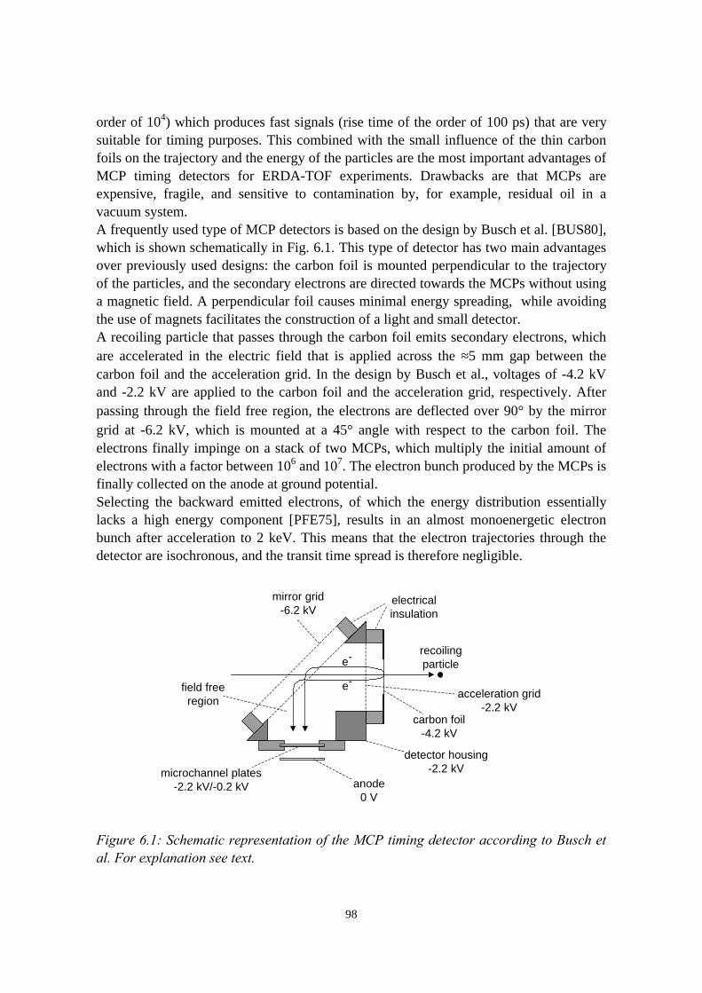
98
order of 104) which produces fast signals (rise time of the order of 100 ps) that are verysuitable for timing purposes. This combined with the small influence of the thin carbonfoils on the trajectory and the energy of the particles are the most important advantages ofMCP timing detectors for ERDA-TOF experiments. Drawbacks are that MCPs areexpensive, fragile, and sensitive to contamination by, for example, residual oil in avacuum system.A frequently used type of MCP detectors is based on the design by Busch et al. [BUS80],which is shown schematically in Fig. 6.1. This type of detector has two main advantagesover previously used designs: the carbon foil is mounted perpendicular to the trajectoryof the particles, and the secondary electrons are directed towards the MCPs without usinga magnetic field. A perpendicular foil causes minimal energy spreading, while avoidingthe use of magnets facilitates the construction of a light and small detector.A recoiling particle that passes through the carbon foil emits secondary electrons, whichare accelerated in the electric field that is applied across the ≈5 mm gap between thecarbon foil and the acceleration grid. In the design by Busch et al., voltages of -4.2 kVand -2.2 kV are applied to the carbon foil and the acceleration grid, respectively. Afterpassing through the field free region, the electrons are deflected over 90° by the mirrorgrid at -6.2 kV, which is mounted at a 45° angle with respect to the carbon foil. Theelectrons finally impinge on a stack of two MCPs, which multiply the initial amount ofelectrons with a factor between 106 and 107. The electron bunch produced by the MCPs isfinally collected on the anode at ground potential.Selecting the backward emitted electrons, of which the energy distribution essentiallylacks a high energy component [PFE75], results in an almost monoenergetic electronbunch after acceleration to 2 keV. This means that the electron trajectories through thedetector are isochronous, and the transit time spread is therefore negligible.
recoilingparticle
e-
e-
carbon foil-4.2 kV
acceleration grid-2.2 kV
mirror grid-6.2 kV
anode0 V
microchannel plates-2.2 kV/-0.2 kV
detector housing-2.2 kV
field freeregion
electricalinsulation
Figure 6.1: Schematic representation of the MCP timing detector according to Busch etal. For explanation see text.
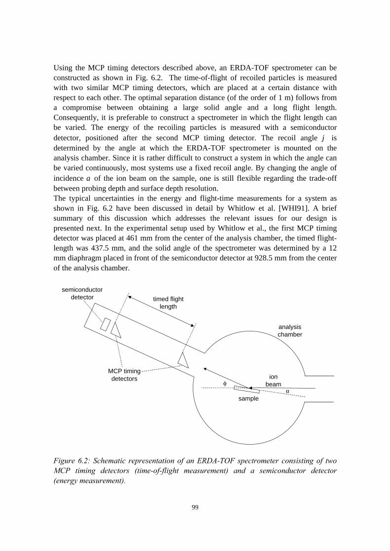
99
Using the MCP timing detectors described above, an ERDA-TOF spectrometer can beconstructed as shown in Fig. 6.2. The time-of-flight of recoiled particles is measuredwith two similar MCP timing detectors, which are placed at a certain distance withrespect to each other. The optimal separation distance (of the order of 1 m) follows froma compromise between obtaining a large solid angle and a long flight length.Consequently, it is preferable to construct a spectrometer in which the flight length canbe varied. The energy of the recoiling particles is measured with a semiconductordetector, positioned after the second MCP timing detector. The recoil angle ϕ isdetermined by the angle at which the ERDA-TOF spectrometer is mounted on theanalysis chamber. Since it is rather difficult to construct a system in which the angle canbe varied continuously, most systems use a fixed recoil angle. By changing the angle ofincidence α of the ion beam on the sample, one is still flexible regarding the trade-offbetween probing depth and surface depth resolution.The typical uncertainties in the energy and flight-time measurements for a system asshown in Fig. 6.2 have been discussed in detail by Whitlow et al. [WHI91]. A briefsummary of this discussion which addresses the relevant issues for our design ispresented next. In the experimental setup used by Whitlow et al., the first MCP timingdetector was placed at 461 mm from the center of the analysis chamber, the timed flight-length was 437.5 mm, and the solid angle of the spectrometer was determined by a 12mm diaphragm placed in front of the semiconductor detector at 928.5 mm from the centerof the analysis chamber.
semiconductordetector
sample
ϕα
ionbeam
MCP timingdetectors
timed flightlength
analysischamber
Figure 6.2: Schematic representation of an ERDA-TOF spectrometer consisting of twoMCP timing detectors (time-of-flight measurement) and a semiconductor detector(energy measurement).
100
Regarding the energy measurement, the energy resolution of the semiconductor detectoris always dominant over the energy spread that results from energy straggling in thecarbon foils and the thickness variations of these foils, provided that the thickness isabout 5 ug/cm2 (≈15 nm) or smaller. The energy resolution ∆E in keV (i.e. the full widthat half maximum of a measured peak that corresponds to monoenergetic particles) ofmodern silicon semiconductors can be estimated as ∆E=A+B⋅E1/3, where A and B areempirical constants and E is the energy of the particles in keV. The empirical constantsdepend strongly on the mass of the particles. Some values for different recoil species aretabulated in reference [HIN90]. As the mass of the detected particles increases, theenergy resolution of semiconductor detectors deteriorates. For example, for oxygenrecoils with an energy between 1 and 15 MeV the energy resolution ∆E lies between 50and 100 keV, while for chlorine recoils ∆E varies from 130 to 320 keV in the sameenergy interval.The uncertainty in the flight-time measurements is composed of three independentcontributions due to (1) the intrinsic time resolution of the MCP timing detectors pluselectronics, (2) straggling and thickness variations in the first carbon foil, and (3) pathlength variations for recoil trajectories through the ERDA-TOF spectrometer. Theintrinsic time resolution of a MCP timing detector is typically about 200 ps, as was foundby various research groups [BUS80, WHI91, DOB98]. This contribution dominates theuncertainty in the flight-time measurement at high recoil energies, for E≥0.1⋅A MeV withA the atomic mass number of the recoil. The time spread due to straggling and thicknessvariations in the first foil of course depends strongly on the thickness of this foil. For 5µg/cm2 carbon foils, as were used by Whitlow et al., straggling and thickness variationsdominate the time spread at low recoil energies (E≤0.1⋅A MeV). Using much thinnercarbon foils, such as the 0.6 µg/cm2 foils that are manufactured by Liechtenstein and co-workers [LIE99], results in a correspondingly smaller time spread. Under the assumptionthat the energy straggling in the foil can be described by Bohr straggling [TES95],replacing a 5 µg/cm2 foil with a 0.6 µg/cm2 foil results in a reduction of the stragglingcontribution with roughly a factor of three. For example: the time spread due tostraggling in the first foil for 1.6 MeV O recoils (i.e. E=0.1⋅A MeV) in a typical ERDA-TOF spectrometer (0.5 m flight length) is ≈180 ps for a 5 µg/cm2 foil and ≈60 ps for a 0.6µg/cm2 foil.The uncertainty in the flight-time measurements due to path length variations of recoiltrajectories through the ERDA-TOF spectrometer is small compared to the othercontributions. The largest path length variations in the system used by Whitlow et al.resulted from the slackness in the carbon foils. In the presence of the electric fieldbetween the foil and the acceleration grid, wrinkles in the foil are stretched out and thesurface becomes bowed. By visual inspection, the distortion was estimated to be 0.5 mmat the center of the foils [WHI91]. For carbon foils that are supported by a grid, such asthe foils prepared by Liechtenstein et al. [LIE99], slackening is not observed and theassociated path length variations can therefore expected to be negligible.
101
An extra contribution to the timing uncertainty that was not discussed by Whitlow et al. isdue to the acceleration/deceleration of low energy recoils of which the charge statechanges as they pass through the first carbon foil. This effect, referred to as the "tandemeffect" by Döbeli et al. [DOB98], results in a few keV energy spread of the particles thatpass the foil, which causes a significant time spread for low recoil energies.An advantage of ERDA-TOF over other ERDA methods, besides the accuratediscrimination between recoils with different mass, is that in principle more accurateenergy measurements are possible by calculating the energy from the measured flight-time. This is due to the fact that the relative timing uncertainties can be significantlysmaller than the relative uncertainties in the energy measurements. For example, Döbeliet al. showed that the energy resolution of their TOF-spectrometer for 1 MeV oxygen wasabout 8 keV, which is about a factor of 5 better than the optimal resolution that can beachieved with silicon semiconductor detectors [DOB98].The ERDA-TOF method also has some drawbacks. The most important disadvantage isthe relatively poor detection efficiency, which is defined as the number of particles thatare actually detected divided by the number of particles that pass through thespectrometer. An important limit for the detection of sufficient electrons on the MCPs toproduce a pulse that exceeds the noise level is the low number of secondary electronsproduced by the particles that pass through the carbon foil. For helium ions with anenergy between 2 and 10 MeV, only 1 to 10 secondary electrons are emitted per ion thatpasses through a 6 µg/cm2 carbon foil. For oxygen recoils with similar energies, thesecondary electron yield is about 50 per ion [CLE73]. The open area ratio of the MCPs,i.e. the ratio between the area formed by the channels and the "dead" area, also plays arole. For most MCPs, the open area ratio is about 0.6. It should be noted that theparticularly low detection sensitivity for helium ions can actually be an advantage forERDA experiments with He+ or α-particle beams, in which scattered beam particles arenot of interest. The detection efficiency is also slightly dependent on the energy of theparticles that pass through the foil, due to the energy dependence of the secondaryelectron yield. For oxygen recoils with energies between 9 and 12.7 MeV, a 5% variationwas observed in reference [WHI89].Another disadvantage of ERDA-TOF is the relatively low count rate due to the smallsolid angle and the limited transmission that results from the grids in the MCP timingdetectors. The small solid angle results from the large distance between thesemiconductor detector and the sample (≈1 m), which is necessary to minimize therelative error of the flight-time measurements. The transmission through two MCP timingdetectors mostly lies between 60 and 70%, depending on the number of grids that is usedand on the transmission of the individual grids.
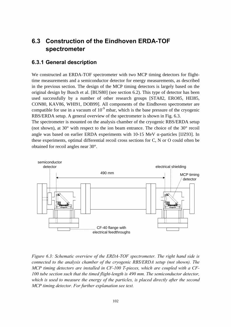
102
6.3 Construction of the Eindhoven ERDA-TOFspectrometer
6.3.1 General description
We constructed an ERDA-TOF spectrometer with two MCP timing detectors for flight-time measurements and a semiconductor detector for energy measurements, as describedin the previous section. The design of the MCP timing detectors is largely based on theoriginal design by Busch et al. [BUS80] (see section 6.2). This type of detector has beenused successfully by a number of other research groups [STA82, ERO85, HEI85,CON80, KAV86, WHI91, DOB99]. All components of the Eindhoven spectrometer arecompatible for use in a vacuum of 10-9 mbar, which is the base pressure of the cryogenicRBS/ERDA setup. A general overview of the spectrometer is shown in Fig. 6.3.The spectrometer is mounted on the analysis chamber of the cryogenic RBS/ERDA setup(not shown), at 30° with respect to the ion beam entrance. The choice of the 30° recoilangle was based on earlier ERDA experiments with 10-15 MeV α-particles [IJZ93]. Inthese experiments, optimal differential recoil cross sections for C, N or O could often beobtained for recoil angles near 30°.
semiconductordetector
490 mm MCP timingdetector
electrical shielding
CF-40 flange withelectrical feedthroughs
Figure 6.3: Schematic overview of the ERDA-TOF spectrometer. The right hand side isconnected to the analysis chamber of the cryogenic RBS/ERDA setup (not shown). TheMCP timing detectors are installed in CF-100 T-pieces, which are coupled with a CF-100 tube section such that the timed flight-length is 490 mm. The semiconductor detector,which is used to measure the energy of the particles, is placed directly after the secondMCP timing detector. For further explanation see text.
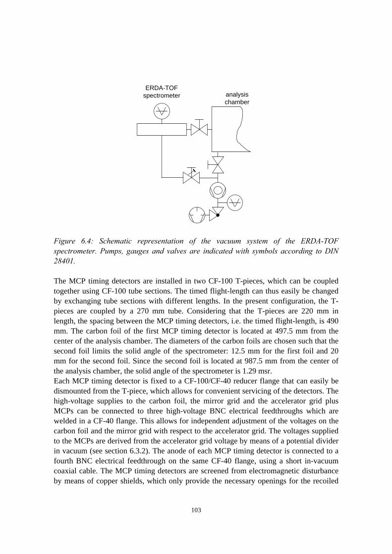
103
analysischamber
ERDA-TOFspectrometer
Figure 6.4: Schematic representation of the vacuum system of the ERDA-TOFspectrometer. Pumps, gauges and valves are indicated with symbols according to DIN28401.
The MCP timing detectors are installed in two CF-100 T-pieces, which can be coupledtogether using CF-100 tube sections. The timed flight-length can thus easily be changedby exchanging tube sections with different lengths. In the present configuration, the T-pieces are coupled by a 270 mm tube. Considering that the T-pieces are 220 mm inlength, the spacing between the MCP timing detectors, i.e. the timed flight-length, is 490mm. The carbon foil of the first MCP timing detector is located at 497.5 mm from thecenter of the analysis chamber. The diameters of the carbon foils are chosen such that thesecond foil limits the solid angle of the spectrometer: 12.5 mm for the first foil and 20mm for the second foil. Since the second foil is located at 987.5 mm from the center ofthe analysis chamber, the solid angle of the spectrometer is 1.29 msr.Each MCP timing detector is fixed to a CF-100/CF-40 reducer flange that can easily bedismounted from the T-piece, which allows for convenient servicing of the detectors. Thehigh-voltage supplies to the carbon foil, the mirror grid and the accelerator grid plusMCPs can be connected to three high-voltage BNC electrical feedthroughs which arewelded in a CF-40 flange. This allows for independent adjustment of the voltages on thecarbon foil and the mirror grid with respect to the accelerator grid. The voltages suppliedto the MCPs are derived from the accelerator grid voltage by means of a potential dividerin vacuum (see section 6.3.2). The anode of each MCP timing detector is connected to afourth BNC electrical feedthrough on the same CF-40 flange, using a short in-vacuumcoaxial cable. The MCP timing detectors are screened from electromagnetic disturbanceby means of copper shields, which only provide the necessary openings for the recoiled
104
particles to pass through and have some small pumping holes. The silicon semiconductordetector, model CU-016-450-300 manufactured by Ortec [PER], is installed on a BNCelectrical feedthrough welded in a CF-100 flange. This flange is mounted directly on theT-piece that contains the second MCP timing detector.The ERDA-TOF spectrometer can be isolated from the analysis chamber of the cryogenicRBS/ERDA setup (see chapter 2) by means of a vacuum valve. The spectrometer canthus be separately vented when servicing is required. Due to the extreme sensitivity of thethin carbon foils to gas flow, initial pumping and venting of the spectrometer takes placethrough a variable leakage valve (see Fig. 6.4), which is connected to the turbomolecularroughing pump of the analysis chamber (see chapter 2).
6.3.2 The MCP timing detectors
The core of the MCP timing detectors is a triangular aluminium housing, on which thecarbon foil, grids and MCPs are mounted (see Fig. 6.5). The carbon foils have beensupplied by Liechtenstein et al. of the Kurchatov Institute, Moscow, already mounted onnickel frames that were especially made for our application. The foils were preparedusing a specialized deposition process [LIE99], by means of which it is possible to obtainfree-standing 0.6 µg/cm2 diamond like carbon foils (≈ 2 nm), supported by a copper gridwith 90% transparency. Such ultra-thin foils are ideal for ERDA-TOF spectrometers,because the spreading in the timing and energy measurements due to straggling andthickness variations in the foils becomes negligible. Similar foils have already beensuccessfully applied in a RBS-TOF system [DOB98]. Initially, we have used 5 µg/cm2
carbon foils for the first test experiments. Electrical contact to the carbon foil is madeusing a copper contact ring (see Fig. 6.5).The grids are electroformed nickel meshes with 95% transparency, part number MN-4manufactured by Buckbee-Mears St. Paul [BUC]. The 32 µm nickel wires have a spacingof 1.27 mm. The grids are clamped when the detector is assembled by simply tighteningthe screws, without using any glue or epoxy. This makes it easy to exchange grids in casethey are damaged during handling, and moreover extra outgassing of the glue or epoxy isavoided. Electrical contact to the mirror grid is made using an aluminium contact ring.The other grids are at the same potential as the detector housing. Because six grids with95% transparency are present in the ERDA-TOF spectrometer, plus two grids with 90%transparency on which the carbon foils are mounted, the transmission of the spectrometeris 60%.Instead of using a commercial MCP assembly, which is fixed in dimensions and offers nopossibility to adjust the voltage over each MCP independently, two single MCPs are usedper detector, model S25-10-D-SET manufactured by Scientific Instruments GmbH [SCI].The MCPs have an active diameter of 25 mm, with an open area (i.e. the summed area ofthe microchannels) that comprises 63% of the total area. Each MCP has a gain of about104 at 900 V bias voltage. Contacts to the MCPs are made using polyimide rings coveredwith a thin gold film (see Fig. 6.5 and Fig. 6.6). The flexible flaps of these contacts are
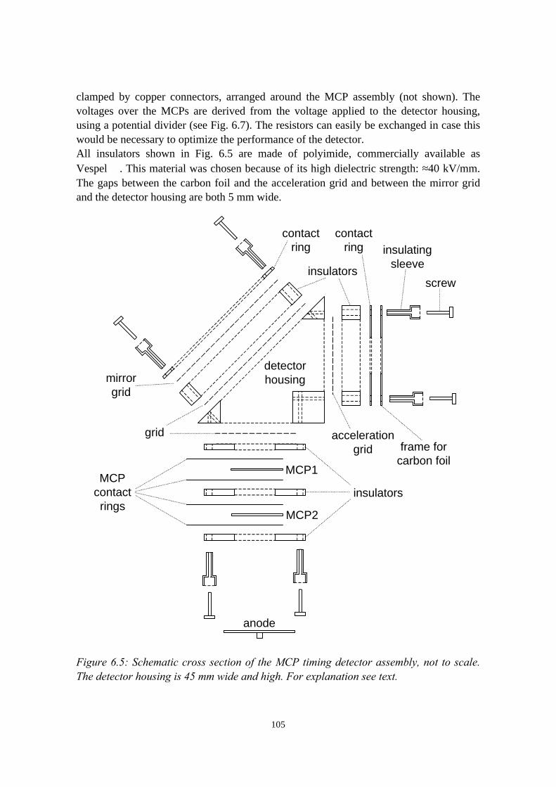
105
clamped by copper connectors, arranged around the MCP assembly (not shown). Thevoltages over the MCPs are derived from the voltage applied to the detector housing,using a potential divider (see Fig. 6.7). The resistors can easily be exchanged in case thiswould be necessary to optimize the performance of the detector.All insulators shown in Fig. 6.5 are made of polyimide, commercially available asVespel . This material was chosen because of its high dielectric strength: ≈40 kV/mm.The gaps between the carbon foil and the acceleration grid and between the mirror gridand the detector housing are both 5 mm wide.
screw
insulatingsleeve
frame forcarbon foil
contactring
insulators
accelerationgrid
mirrorgrid
contactring
grid
MCPcontactrings
MCP1
MCP2
insulators
detectorhousing
anode
Figure 6.5: Schematic cross section of the MCP timing detector assembly, not to scale.The detector housing is 45 mm wide and high. For explanation see text.
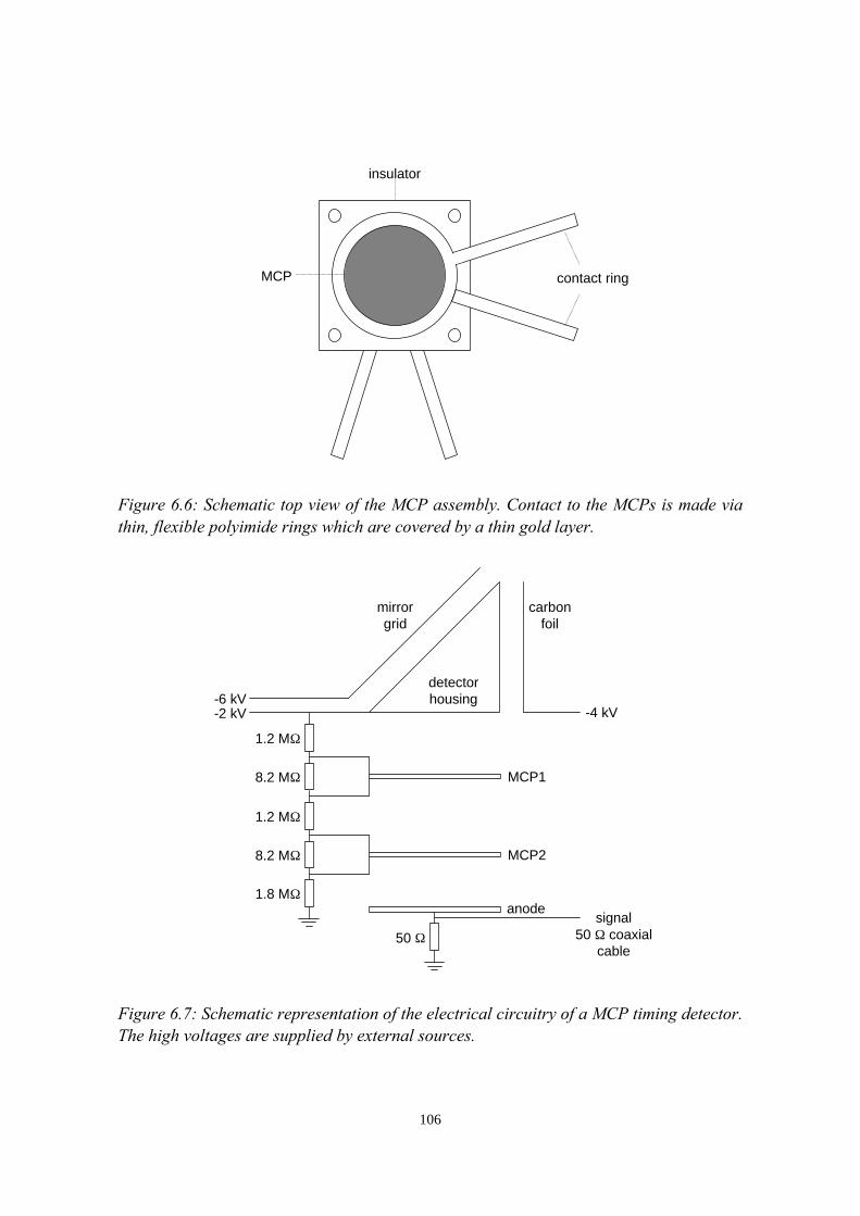
106
insulator
contact ringsMCP
Figure 6.6: Schematic top view of the MCP assembly. Contact to the MCPs is made viathin, flexible polyimide rings which are covered by a thin gold layer.
-4 kV-6 kV-2 kV
signal
50 Ω
1.2 MΩ
8.2 MΩ
1.2 MΩ
8.2 MΩ
1.8 MΩ
MCP2
MCP1
anode
carbonfoil
mirrorgrid
detectorhousing
50 Ω coaxialcable
Figure 6.7: Schematic representation of the electrical circuitry of a MCP timing detector.The high voltages are supplied by external sources.
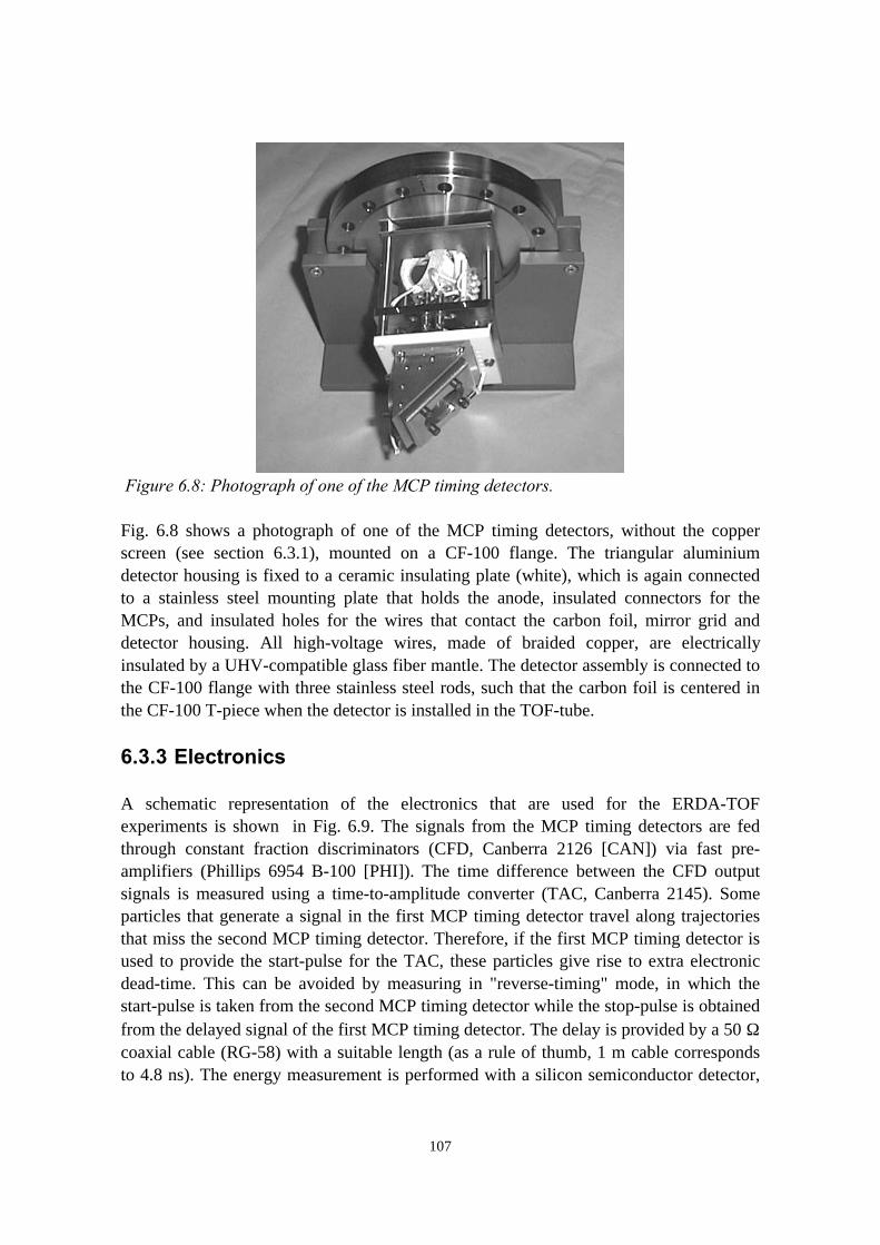
107
Figure 6.8: Photograph of one of the MCP timing detectors.
Fig. 6.8 shows a photograph of one of the MCP timing detectors, without the copperscreen (see section 6.3.1), mounted on a CF-100 flange. The triangular aluminiumdetector housing is fixed to a ceramic insulating plate (white), which is again connectedto a stainless steel mounting plate that holds the anode, insulated connectors for theMCPs, and insulated holes for the wires that contact the carbon foil, mirror grid anddetector housing. All high-voltage wires, made of braided copper, are electricallyinsulated by a UHV-compatible glass fiber mantle. The detector assembly is connected tothe CF-100 flange with three stainless steel rods, such that the carbon foil is centered inthe CF-100 T-piece when the detector is installed in the TOF-tube.
6.3.3 Electronics
A schematic representation of the electronics that are used for the ERDA-TOFexperiments is shown in Fig. 6.9. The signals from the MCP timing detectors are fedthrough constant fraction discriminators (CFD, Canberra 2126 [CAN]) via fast pre-amplifiers (Phillips 6954 B-100 [PHI]). The time difference between the CFD outputsignals is measured using a time-to-amplitude converter (TAC, Canberra 2145). Someparticles that generate a signal in the first MCP timing detector travel along trajectoriesthat miss the second MCP timing detector. Therefore, if the first MCP timing detector isused to provide the start-pulse for the TAC, these particles give rise to extra electronicdead-time. This can be avoided by measuring in "reverse-timing" mode, in which thestart-pulse is taken from the second MCP timing detector while the stop-pulse is obtainedfrom the delayed signal of the first MCP timing detector. The delay is provided by a 50 Ωcoaxial cable (RG-58) with a suitable length (as a rule of thumb, 1 m cable correspondsto 4.8 ns). The energy measurement is performed with a silicon semiconductor detector,

108
using a charge sensitive pre-amplifier (Ortec 142A [PER]) and a main amplifier with 1 µsshaping time (Ortec 410). The signals obtained from the TAC (flight-time measurement)and the main amplifier (energy measurement) are delayed and stretched using linear-gate&stretcher modules (LGS Ortec 542) such that flat-topped signals are obtained thatfall within the same ≈1.5 µs time window. The LGS outputs are connected to a dualmulti-channel analyzer (MCA) that is part of our multi-parameter data-acquisition system[SIM98]. The trigger pulse for the MCA is provided by the delayed valid-conversionsignal from the TAC. This signal is generated when the TAC receives a start-pulse and astop-pulse within its measurement time window, i.e. when a flight-time measurement isperformed.
semi-conductordetector
pre-amp
TAC
main-amp
stop
start
MCALGS
µs delay
TE
MCPdetector
1
fast pre-amp
MCPdetector
2
fast pre-amp
CFD
CFD
delaycable
LGS
validconversion
trigger
Figure 6.9: Schematic representation of the ERDA-TOF electronics. For explanation seetext.
6.4 Performance
A first series of test-experiments have been performed with the ERDA-TOFspectrometer, using 5 µg/cm2 carbon foils in the MCP timing detectors. The experimentswere carried out with a 13.4 MeV α-particle beam on a sample consisting of a 80 nmSi2O3N film deposited on a silicon substrate. The sample was rotated such that the anglebetween the ion beam and the sample surface was 20°. The detection angle of the ERDA-TOF spectrometer is fixed at 30°, as explained in section 6.3.1.Fig. 6.10 shows a scatter plot of the time difference T between the signals of the twoMCP timing detectors versus the energy E of the detected particles. The measurementwas carried out in the reverse timing mode, which is explained in section 6.3.3. Thesignal obtained from the first MCP timing detector was delayed with 173 ns with respectto the signal provided by the second MCP timing detector, using ≈36 m RG-58 coaxialcable. The measurement range of the TAC was set to 200 ns. The fastest particles, whichare 12.9 MeV α-particles scattered from silicon atoms at the surface, travel the 490 mmflight-length of the ERDA-TOF spectrometer in 20 ns. This means that for theseparticles, the time difference between the signals of the two MCP timing detectors T is
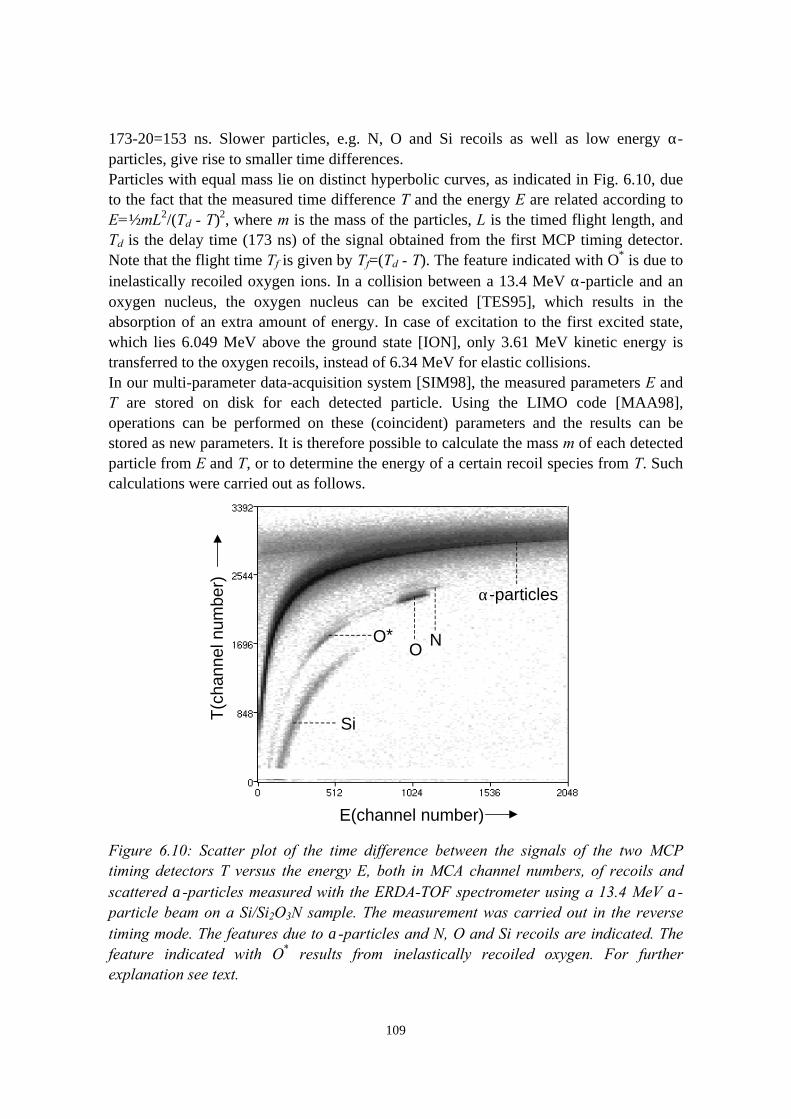
109
173-20=153 ns. Slower particles, e.g. N, O and Si recoils as well as low energy α-particles, give rise to smaller time differences.Particles with equal mass lie on distinct hyperbolic curves, as indicated in Fig. 6.10, dueto the fact that the measured time difference T and the energy E are related according toE=½mL2/(Td - T)2, where m is the mass of the particles, L is the timed flight length, andTd is the delay time (173 ns) of the signal obtained from the first MCP timing detector.Note that the flight time Tf is given by Tf=(Td - T). The feature indicated with O* is due toinelastically recoiled oxygen ions. In a collision between a 13.4 MeV α-particle and anoxygen nucleus, the oxygen nucleus can be excited [TES95], which results in theabsorption of an extra amount of energy. In case of excitation to the first excited state,which lies 6.049 MeV above the ground state [ION], only 3.61 MeV kinetic energy istransferred to the oxygen recoils, instead of 6.34 MeV for elastic collisions.In our multi-parameter data-acquisition system [SIM98], the measured parameters E andT are stored on disk for each detected particle. Using the LIMO code [MAA98],operations can be performed on these (coincident) parameters and the results can bestored as new parameters. It is therefore possible to calculate the mass m of each detectedparticle from E and T, or to determine the energy of a certain recoil species from T. Suchcalculations were carried out as follows.
E(channel number)
T(c
hann
el n
umbe
r)
α-particles
ON
Si
O*
Figure 6.10: Scatter plot of the time difference between the signals of the two MCPtiming detectors T versus the energy E, both in MCA channel numbers, of recoils andscattered α-particles measured with the ERDA-TOF spectrometer using a 13.4 MeV α-particle beam on a Si/Si2O3N sample. The measurement was carried out in the reversetiming mode. The features due to α-particles and N, O and Si recoils are indicated. Thefeature indicated with O* results from inelastically recoiled oxygen. For furtherexplanation see text.
110
Figure 6.11: T as a function of E for α-particles, O recoils and Si recoils. The data pointswere picked off the hyperbolic curves in the T versus E scatter plot. The solid linescorrespond to least squares fits. For further explanation see text.
By picking points off the hyperbolic curves corresponding to α-particles, O and Si,respectively, data-sets of E versus T for these particles were obtained, expressed in MCAchannel numbers. Least squares fits were subsequently carried out for each data-setaccording to E=mA/(B - T)2 + C, where m is the particle mass in atomic mass units and A,B and C are fit variables. The variable C was introduced to account for the small offset inthe energy measurements. Fig. 6.11 shows a plot of the picked data points and thecorresponding least squares fits. The fitted values of A and B for the different curves weresimilar within 7% and 2%, respectively, while the energy offset C varied between 52 and94 channel numbers. With LIMO, four different mass-parameters mE,T were calculatedfrom E and T, according to mE,T=(E - C)(B - T)2/A using either A, B and C as determinedfor the three different data-sets in Fig. 6.11 or mean values for A, B and C. Three extraenergy-parameters ET were also calculated from T according to ET=mA/(B - T)2 + C forα-particles, O recoils and Si recoils using the corresponding masses and values of the fitvariables.Fig. 6.12 shows a scatter plot of the calculated mass versus the measured energy. Themass was calculated using A, B and C fitted for the oxygen data-set in Fig. 6.11. Usingthe fit variables of the other data-sets or the mean values of A, B and C resulted in largelysimilar plots. ERDA spectra of the individual recoil species can be obtained by selectingregions in the mass versus energy scatter plot and projecting the counts inside the regionson the energy axis. This is shown in Fig. 6.13 for oxygen recoils. Two distinct peaks canbe seen in the ERDA spectrum, due to elastic and inelastic recoiling of oxygen.
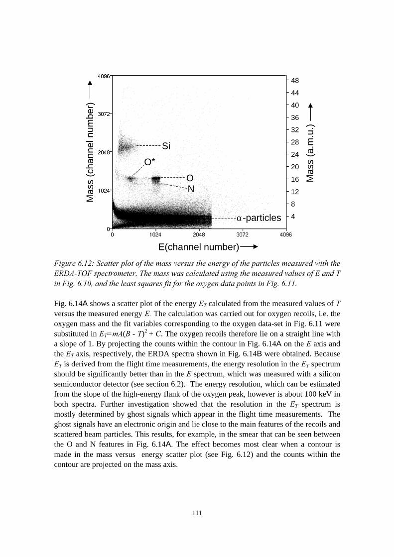
111
E(channel number)
Mas
s (c
hann
el n
umbe
r)
α-particles
ON
Si
O*
4
8
12
16
20
24
28
32
36
40
44
48
Mas
s (a
.m.u
.)
Figure 6.12: Scatter plot of the mass versus the energy of the particles measured with theERDA-TOF spectrometer. The mass was calculated using the measured values of E and Tin Fig. 6.10, and the least squares fit for the oxygen data points in Fig. 6.11.
Fig. 6.14A shows a scatter plot of the energy ET calculated from the measured values of Tversus the measured energy E. The calculation was carried out for oxygen recoils, i.e. theoxygen mass and the fit variables corresponding to the oxygen data-set in Fig. 6.11 weresubstituted in ET=mA(B - T)2 + C. The oxygen recoils therefore lie on a straight line witha slope of 1. By projecting the counts within the contour in Fig. 6.14A on the E axis andthe ET axis, respectively, the ERDA spectra shown in Fig. 6.14B were obtained. BecauseET is derived from the flight time measurements, the energy resolution in the ET spectrumshould be significantly better than in the E spectrum, which was measured with a siliconsemiconductor detector (see section 6.2). The energy resolution, which can be estimatedfrom the slope of the high-energy flank of the oxygen peak, however is about 100 keV inboth spectra. Further investigation showed that the resolution in the ET spectrum ismostly determined by ghost signals which appear in the flight time measurements. Theghost signals have an electronic origin and lie close to the main features of the recoils andscattered beam particles. This results, for example, in the smear that can be seen betweenthe O and N features in Fig. 6.14A. The effect becomes most clear when a contour ismade in the mass versus energy scatter plot (see Fig. 6.12) and the counts within thecontour are projected on the mass axis.
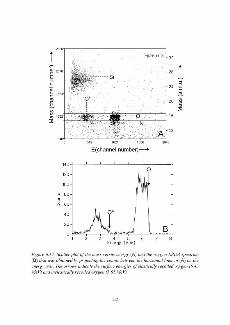
112
E(channel number)
Mas
s (c
hann
el n
umbe
r)
12
16
20
24
28
32
Mas
s (a
.m.u
.)
A
ON
Si
O*
O
O*
B
Figure 6.13: Scatter plot of the mass versus energy (A) and the oxygen ERDA spectrum(B) that was obtained by projecting the counts between the horizontal lines in (A) on theenergy axis. The arrows indicate the surface energies of elastically recoiled oxygen (6.43MeV) and inelastically recoiled oxygen (3.61 MeV).
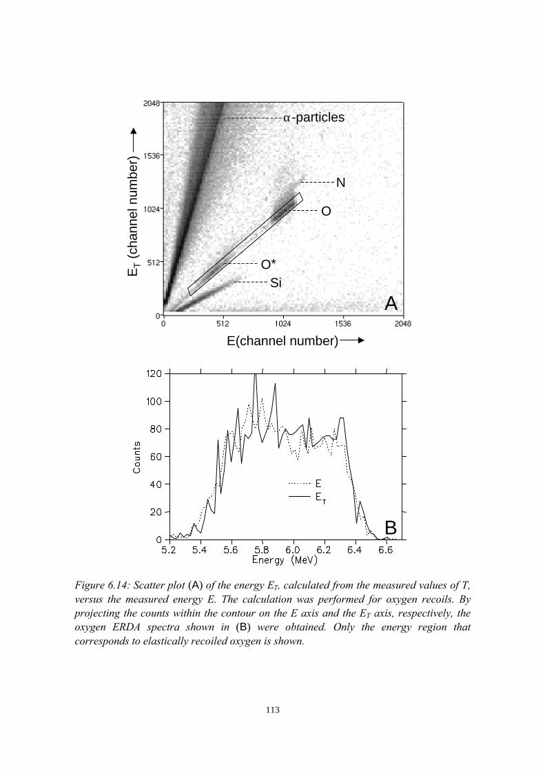
113
α-particles
O
N
SiO*
E(channel number)
ET (
chan
nel n
umbe
r)
A
B
Figure 6.14: Scatter plot (A) of the energy ET, calculated from the measured values of T,versus the measured energy E. The calculation was performed for oxygen recoils. Byprojecting the counts within the contour on the E axis and the ET axis, respectively, theoxygen ERDA spectra shown in (B) were obtained. Only the energy region thatcorresponds to elastically recoiled oxygen is shown.
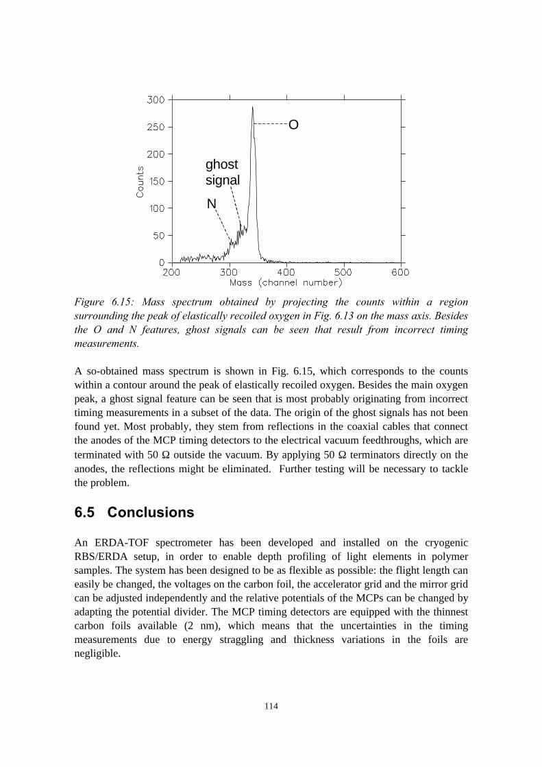
114
O
N
ghostsignal
Figure 6.15: Mass spectrum obtained by projecting the counts within a regionsurrounding the peak of elastically recoiled oxygen in Fig. 6.13 on the mass axis. Besidesthe O and N features, ghost signals can be seen that result from incorrect timingmeasurements.
A so-obtained mass spectrum is shown in Fig. 6.15, which corresponds to the countswithin a contour around the peak of elastically recoiled oxygen. Besides the main oxygenpeak, a ghost signal feature can be seen that is most probably originating from incorrecttiming measurements in a subset of the data. The origin of the ghost signals has not beenfound yet. Most probably, they stem from reflections in the coaxial cables that connectthe anodes of the MCP timing detectors to the electrical vacuum feedthroughs, which areterminated with 50 Ω outside the vacuum. By applying 50 Ω terminators directly on theanodes, the reflections might be eliminated. Further testing will be necessary to tacklethe problem.
6.5 Conclusions
An ERDA-TOF spectrometer has been developed and installed on the cryogenicRBS/ERDA setup, in order to enable depth profiling of light elements in polymersamples. The system has been designed to be as flexible as possible: the flight length caneasily be changed, the voltages on the carbon foil, the accelerator grid and the mirror gridcan be adjusted independently and the relative potentials of the MCPs can be changed byadapting the potential divider. The MCP timing detectors are equipped with the thinnestcarbon foils available (2 nm), which means that the uncertainties in the timingmeasurements due to energy straggling and thickness variations in the foils arenegligible.
115
The first test experiments have demonstrated that scattered beam particles and recoilswith different mass can clearly be separated. Therefore, depth profiling of single recoilspecies has become possible. Further improvements are necessary to deal with the ghostsignals, which most probably originate from reflections due to improper impedancematching. This is expected to considerably improve the energy resolution and massresolving power.
References
[BUC] Buckbee-Mears St. Paul (http://devicelink.com/company98/b/b00141.html), St. Paul, MN 55101, USA
[BUS80] F. Busch, W. Pfeffer, B. Kohlmeyer, D. Schüll, F. Pühlhoffer, Nucl. Instr.and Meth. 171 (1980) 71
[CAN] Canberra Industries (www.canberra.com), Meriden, CT 06450, USA[CLE73] H.G. Clerc, H.J. Gehrhardt, L. Richter, K.H. Schmidt, Nucl. Instr. and
Meth. 113 (1973) 325[CON80] L. Conradi et al., Nucl. Instr. and Meth. A297 (1980) 461[DOB98] M. Döbeli, R.M. Ender, V. Liechtenstein, D. Vetterli, Nucl. Instr. and
Meth. B142 (1998) 417[ERO85] G. D'Erosmo, V. Paticchio, A. Pantaleo, Nucl. Instr. and Meth. A234
(1985) 91[GEL71] C.K. Gelbke, K.D. Hildenbrand, R. Bock, Nucl. Instr. and Meth. 95 (1971)
397[HEI85] R.D. Heil, J. Drexler, K. Huber, U. Kneissl, G. Mank, H. Ries, H. Ströler,
T. Weber, W. Wilke, Nucl. Instr. and Meth. A239 (1985) 545[HIN90] P.F. Hinrichsen, D.W. Hetherington, S.C. Gujrathi, L. Cliche, Nucl. Instr.
and Meth. B45 (1990) 275[IJZ93] L.J. van IJzendoorn, H.A. Rijken, S.S. Klein, M.J.A. de Voigt, Appl. Surf.
Sci. 70/71 (1993) 58[ION] Ion beam analysis table of the elements, http://www.sandia.gov/1100/
1111/Elements/tablefr.htm[KAV85] R.L. Kavlov, Y.L. Margaryan, M.G. Panyan, G.A. Papyan, Nucl. Instr.
and Meth. A237 (1985) 543[LIE99] V.Kh. Liechtenstein, T.M. Ivkova, E.D. Olshanski, A.M. Baranov, R.
Repnow, R. Hellborg, R.A. Weller, H.L. Wirth, Nucl. Instr. and Meth.A438 (1999) 79
[MAA98] A.J.H. Maas, Elastic recoil detection analysis with α-particles, (PhDDissertation, Eindhoven University of Technology, 1998)
[PER] PerkinElmer Instruments, Ortec products, formerly EG&G Ortec(www.perkinelmer.com), Norwalk, CT 06859-0001, USA
[PFE75] K.E. Pferdekämper, H.G. Clerc, Z. Phys. A275 (1975) 223[PHI] Phillips Scientific (www.philipsscientific.com), Ramsey, NJ 07446, USA
116
[PLE71] H. Pleyer, B. Kohlmeyer, W.F.W. Schneider and R. Bock, Nucl. Instr. andMeth. 96 (1971) 263
[RIC95] R.W. Richards, Scattering methods in polymer science, (London, EllisHorwood, 1995)
[SCI] Scientific Instruments GmbH, www.scientificinstruments.com, West PalmBeach, FL 33407, USA
[SIM98] D.P.L. Simons, Data acquisition, detector technology, and materialsanalysis with a scanning ion microprobe, (PhD Dissertation, EindhovenUniversity of Technology, 1998)
[STA82] W. Starechi, A.M. Stefanini, S. Lunardi, C. Signorini, Nucl. Instr. andMeth. 193 (1982) 499
[STE76] H. Stelzer, Nucl. Instr. and Meth. 133 (1976) 409[TES95] J.R. Tesmer, M. Nastasi, Handbook of modern ion beam materials
analysis, (Materials Research Society, Pittsburg, 1995)[WHI89] H.J. Whitlow, A.B.C. Andersson, C. S. Petersson, Nucl. Instr. and Meth.
B36 (1989) 53[WHI91] H.J. Whitlow, B. Jakobsson, L. Westerberg, Nucl. Instr. and Meth. A310
(1991) 636
117
7) The stability of the interface betweenOC1C10-PPV and PEDOT:PSS
7.1 Introduction
A commonly used hole-injecting contact in polymer light emitting diodes (pLEDs) isindium-tin-oxide (ITO), due to its suitable work function (≈4.5 eV) and its hightransparency for visible light. Moreover, ITO has a low resistivity and can easily bepatterned. However, the interface between ITO and the semiconducting polymers that areapplied in pLEDs is in general not stable. Indium containing species can migrate into thepolymer (see chapter 4), which results in unintentional doping [BRU97]. Additionally,oxidation of electroluminescent polymers by oxygen diffusing out of the ITO has beenobserved [SCO96].A possible way to deal with these problems is the introduction of an organic holetransport layer between the ITO and the emissive polymer, which has indeed led to adramatic improvement of the device lifetime and also the luminous efficiency [BER98,KAR96, CAR97]. Suitable materials for such a hole transport layer are heavily dopedpolyaniline (PANI) or poly-(3,4-ethylene-dioxythiophene) (PEDOT) [SCO96]. One ofthe most commonly used materials is PEDOT doped with poly(styrenesulfonate) (PSS),which can be deposited by spin coating from an aqueous solution [JON94].Although the introduction of a PEDOT:PSS hole transport layer in pLEDs has resulted ina major improvement of the devices in terms of lifetime and luminous efficiency, newproblems may arise that are associated with the PEDOT:PSS film [KIM99]. In otherwords: the stability of the ITO/PEDOT:PSS and PEDOT:PSS/emissive-polymerinterfaces may also play a role in the degradation of the pLEDs, even though the moreimportant degradation processes due to the direct contact between ITO and the emissivepolymer are suppressed. It has already been shown that the ITO/PEDOT:PSS interface isnot stable (see chapter 4), due to the hygroscopic and acidic nature of PSS, which reactswith water to form H3O
+ and H2SO4.It is interesting to study whether there is migration of species originating from thePEDOT:PSS film into the emissive polymer. Since both PEDOT molecules and PSSmolecules contain sulphur, such species are also likely to contain sulphur atoms.In this chapter, the stability of the interface between PEDOT:PSS and the emissivepolymer, OC1C10-poly-(phenylenevinylene) (OC1C10-PPV) is investigated in a fullworking device structure. Using cryogenic RBS, we studied possible migration of sulphurcompounds originating from the PEDOT:PSS film, stimulated by device operation,annealing and exposure to air, respectively. Cryogenic RBS has the advantage thatquantitative depth profiling is possible, without destroying the pLED samples during themeasurements thanks to the strong reduction of ion beam induced damage by samplecooling (see chapter 3). A disadvantage is that depth profiling of sulphur in pLEDs with

118
an ITO anode with RBS is cumbersome due to the signal that arises from the relativelyheavy indium atoms in the ITO layer. For such samples, a large indium peak appears at arelatively high energy in the RBS spectrum, with a tail that extends towards lowerenergies due to multiple scattering of the projectile ions at indium atoms in the ITO layer.This multiple scattering tail strongly limits the detection sensitivity for small amounts ofsulphur. This is demonstrated in Fig. 7.1, which shows an RBS spectrum of a pLEDconsisting of a glass substrate, an ITO anode, a PEDOT:PSS hole transport layer, anOC1C-10-PPV emissive film, a low work function (φ ) metal cathode and an aluminiumcapping. Such a pLED will be referred to as a "standard" pLED in the remainder of thischapter. Two distinct peaks can be seen in the RBS spectrum: a large indium peak atabout 1.5 MeV due to indium in the ITO anode and an aluminium peak at the Al surfaceenergy (1.11 MeV) that arises from the aluminium capping. Also features due to the glasssubstrate and sulphur in the PEDOT:PSS film can be seen. A signal due to sulphur isalways superimposed on the multiple scattering tail of the indium peak. This problem canbe solved by replacing ITO with aluminium. Therefore, we prepared model pLEDs withan aluminium anode, covered by a thin silver protection layer (see section 7.2). The silverlayer was introduced to protect the aluminium from the acidic aqueous solution fromwhich the PEDOT:PSS hole transport layer was cast. Otherwise, the model pLEDs weresimilar to the standard pLEDs. Apart from depth profiling with RBS (see section 7.3),electrical characterisation of the pLEDs was carried out (see section 7.4), before and afterdegradation due to operation of the devices.
S
Al
S
2 MeVHe+
170°RBS
PEDOT:PSSPPV
low φ metal
glass
IT O
Al
In
multiplescattering tail
glasssubstrate
Figure 7.1: RBS spectrum of a standard pLED with an ITO anode. The solid arrowsindicate the surface energies of sulphur (1.22 MeV) and aluminium (1.11 MeV). Signalsdue to sulphur are always superimposed on the multiple scattering tail of the largeindium peak.
119
7.2 Sample preparation and experimental methods
Sample preparationThe preparation of the model pLED samples was carried out according to the followingprocedure. Glass substrates were cleaned with several detergents, followed by a 15minutes UV ozone treatment. The substrates were subsequently introduced into a vapourdeposition chamber, which was installed inside a glove box with a nitrogen atmosphere.Aluminium anodes, with a thickness of ≈200 nm as measured with a quartz crystalmicrobalance, were deposited by evaporation through a mask. A ≈8 nm silver film wasdeposited on top of the aluminium anodes to protect these against the acid aqueousPEDOT:PSS solution, from which ≈200 nm PEDOT:PSS hole transport layers weredeposited by spin coating in air. Retained water was removed from the PEDOT:PSS filmsby annealing in air at 150 °C during 5 minutes. Directly after this treatment, the sampleswere transferred to the glove box that contained the vapour deposition chamber, where asimilar annealing treatment was carried out. Subsequently, a ≈200 nm OC1C10-PPVemissive film was deposited by spin coating inside the glove box from a 1 wt.% solutionin toluene. Finally, cathodes consisting of a ≈5 nm low work function metal covered by a≈70 nm aluminium capping were deposited by evaporation through a mask.
Electrical characterisation, electrical stress experimentsThe current density J versus voltage V characteristics of the devices were measured witha HP4140B [HEW] DC voltage-source/pA-meter, which was installed in the glove boxunder nitrogen atmosphere. Since the model pLEDs did not have a transparent electrode,the light output could not be measured.To study the effects of device degradation, the pLEDs were electrically stressed byapplying either a constant voltage or a constant current. The electrical stress experimentswere also carried out inside the glove box under nitrogen atmosphere. The samples wereannealed on a hot plate at 70 °C during electrical stress, in order to accelerate degradationprocesses.
RBS measurementsThe RBS experiments were carried out with a 2 MeV He+ beam, using the cryogenicRBS/ERDA setup (see chapter 2). The detector was placed at 170° with respect to the ionbeam, and the sample was rotated such that the angle between the sample normal and theion beam was 45°. This RBS geometry proved to be optimal for depth profiling ofsulphur in the OC1C10-PPV film of the model pLED samples.Using the load lock system of the cryogenic RBS/ERDA setup with its portable vacuumcontainer (see chapter 2), the samples were transferred to the setup without exposure toair. All experiments were carried out at cryogenic temperatures, which was essential toavoid destructive gas bubble formation in the samples (see chapter 3).
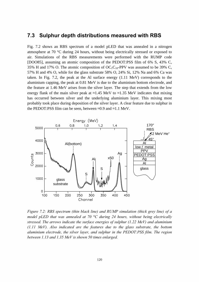
120
7.3 Sulphur depth distributions measured with RBS
Fig. 7.2 shows an RBS spectrum of a model pLED that was annealed in a nitrogenatmosphere at 70 °C during 24 hours, without being electrically stressed or exposed toair. Simulations of the RBS measurements were performed with the RUMP code[DOO85], assuming an atomic composition of the PEDOT:PSS film of 6% S, 43% C,35% H and 17% O. The atomic composition of OC1C10-PPV was assumed to be 39% C,57% H and 4% O, while for the glass substrate 58% O, 24% Si, 12% Na and 6% Ca wastaken. In Fig. 7.2, the peak at the Al surface energy (1.11 MeV) corresponds to thealuminium capping, the peak at 0.81 MeV is due to the aluminium bottom electrode, andthe feature at 1.46 MeV arises from the silver layer. The step that extends from the lowenergy flank of the main silver peak at ≈1.45 MeV to ≈1.35 MeV indicates that mixinghas occurred between silver and the underlying aluminium layer. This mixing mostprobably took place during deposition of the silver layer. A clear feature due to sulphur inthe PEDOT:PSS film can be seen, between ≈0.9 and ≈1.1 MeV.
x50
glasssubstrate
Al(bottom)
S
Al
S
Ag
45°
2 MeV He+
170°RBS
PEDOT:PSSPPV
low φ metal
glass
AlAg
Al
Figure 7.2: RBS spectrum (thin black line) and RUMP simulation (thick grey line) of amodel pLED that was annealed at 70 °C during 24 hours, without being electricallystressed. The arrows indicate the surface energies of sulphur (1.22 MeV) and aluminium(1.11 MeV). Also indicated are the features due to the glass substrate, the bottomaluminium electrode, the silver layer, and sulphur in the PEDOT:PSS film. The regionbetween 1.13 and 1.35 MeV is shown 50 times enlarged.
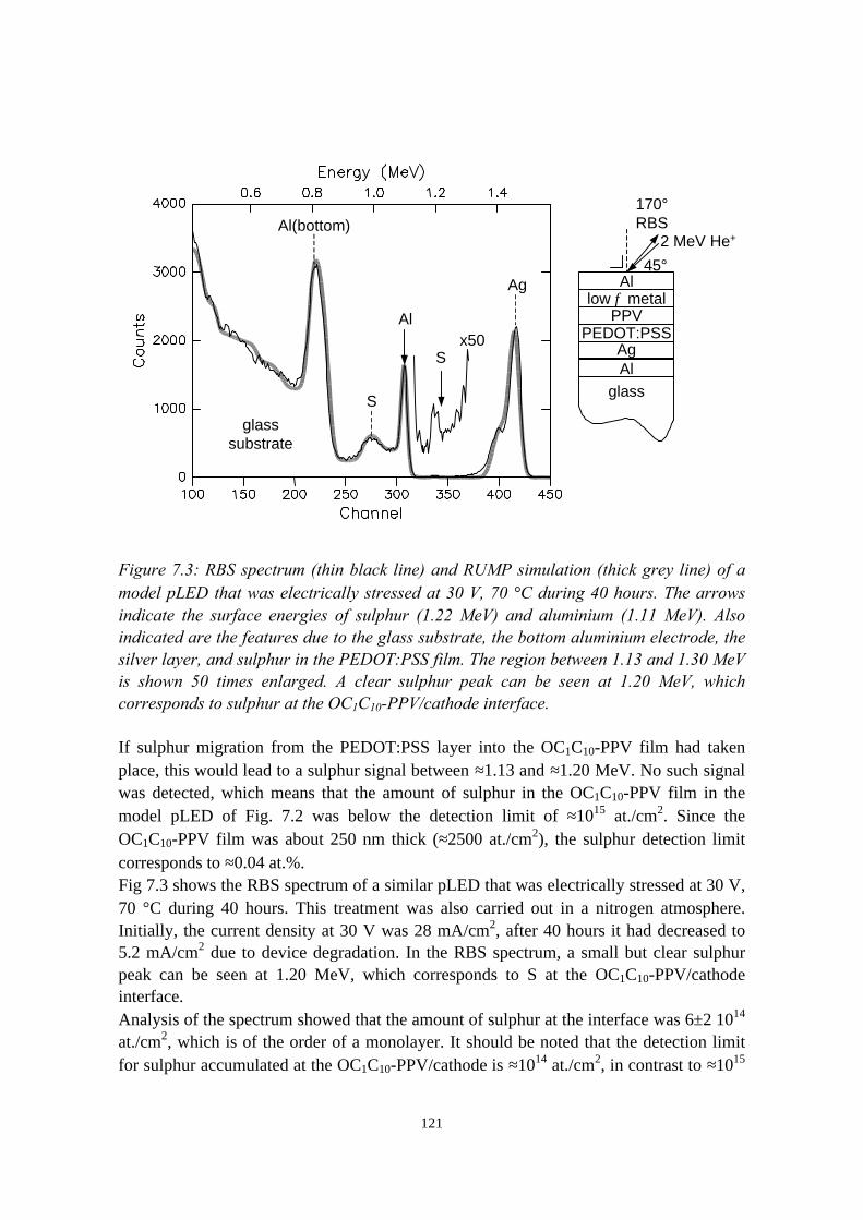
121
x50
glasssubstrate
Al(bottom)
S
Al
S
Ag45°
2 MeV He+
170°RBS
PEDOT:PSSPPV
low φ metal
glass
AlAg
Al
Figure 7.3: RBS spectrum (thin black line) and RUMP simulation (thick grey line) of amodel pLED that was electrically stressed at 30 V, 70 °C during 40 hours. The arrowsindicate the surface energies of sulphur (1.22 MeV) and aluminium (1.11 MeV). Alsoindicated are the features due to the glass substrate, the bottom aluminium electrode, thesilver layer, and sulphur in the PEDOT:PSS film. The region between 1.13 and 1.30 MeVis shown 50 times enlarged. A clear sulphur peak can be seen at 1.20 MeV, whichcorresponds to sulphur at the OC1C10-PPV/cathode interface.
If sulphur migration from the PEDOT:PSS layer into the OC1C10-PPV film had takenplace, this would lead to a sulphur signal between ≈1.13 and ≈1.20 MeV. No such signalwas detected, which means that the amount of sulphur in the OC1C10-PPV film in themodel pLED of Fig. 7.2 was below the detection limit of ≈1015 at./cm2. Since theOC1C10-PPV film was about 250 nm thick (≈2500 at./cm2), the sulphur detection limitcorresponds to ≈0.04 at.%.Fig 7.3 shows the RBS spectrum of a similar pLED that was electrically stressed at 30 V,70 °C during 40 hours. This treatment was also carried out in a nitrogen atmosphere.Initially, the current density at 30 V was 28 mA/cm2, after 40 hours it had decreased to5.2 mA/cm2 due to device degradation. In the RBS spectrum, a small but clear sulphurpeak can be seen at 1.20 MeV, which corresponds to S at the OC1C10-PPV/cathodeinterface.Analysis of the spectrum showed that the amount of sulphur at the interface was 6±2⋅1014
at./cm2, which is of the order of a monolayer. It should be noted that the detection limitfor sulphur accumulated at the OC1C10-PPV/cathode is ≈1014 at./cm2, in contrast to ≈1015
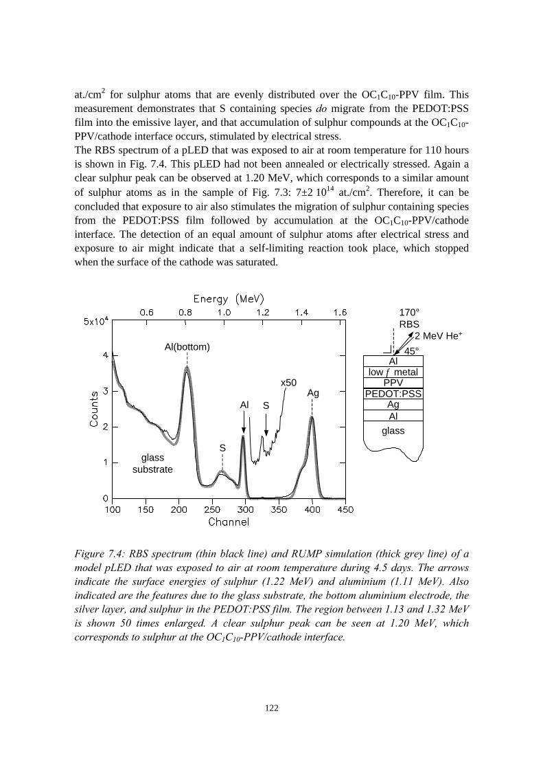
122
at./cm2 for sulphur atoms that are evenly distributed over the OC1C10-PPV film. Thismeasurement demonstrates that S containing species do migrate from the PEDOT:PSSfilm into the emissive layer, and that accumulation of sulphur compounds at the OC1C10-PPV/cathode interface occurs, stimulated by electrical stress.The RBS spectrum of a pLED that was exposed to air at room temperature for 110 hoursis shown in Fig. 7.4. This pLED had not been annealed or electrically stressed. Again aclear sulphur peak can be observed at 1.20 MeV, which corresponds to a similar amountof sulphur atoms as in the sample of Fig. 7.3: 7±2⋅1014 at./cm2. Therefore, it can beconcluded that exposure to air also stimulates the migration of sulphur containing speciesfrom the PEDOT:PSS film followed by accumulation at the OC1C10-PPV/cathodeinterface. The detection of an equal amount of sulphur atoms after electrical stress andexposure to air might indicate that a self-limiting reaction took place, which stoppedwhen the surface of the cathode was saturated.
45°
2 MeV He+
170°RBS
PEDOT:PSSPPV
low φ metal
glass
AlAg
Al
x50
glasssubstrate
Al(bottom)
SAl
S
Ag
Figure 7.4: RBS spectrum (thin black line) and RUMP simulation (thick grey line) of amodel pLED that was exposed to air at room temperature during 4.5 days. The arrowsindicate the surface energies of sulphur (1.22 MeV) and aluminium (1.11 MeV). Alsoindicated are the features due to the glass substrate, the bottom aluminium electrode, thesilver layer, and sulphur in the PEDOT:PSS film. The region between 1.13 and 1.32 MeVis shown 50 times enlarged. A clear sulphur peak can be seen at 1.20 MeV, whichcorresponds to sulphur at the OC1C10-PPV/cathode interface.

123
Since the only material in the pLEDs that contains sulphur is PEDOT:PSS, the sulphurcontaining species that were detected at the interface between OC1C10-PPV and thecathode must originate from the PEDOT:PSS hole transport layer. Both PEDOT and PSSmolecules contain sulphur (see Fig. 7.5), however migration of these large moleculesthrough OC1C10-PPV seems very unlikely. As in all polymers, there is a certaindistribution in molecular size, which means that the presence of small PEDOT or PSSpolymer/oligomer molecules can not be excluded. Such small molecules could diffusemore easily through the OC1C10-PPV. Due to the fact that PEDOT is heavily doped inPEDOT:PSS, the small PEDOT molecules could be positively charged, which means thatthey could migrate towards the cathode when the pLED is operated at forward bias.Although this could explain the detection of sulphur at the OC1C10-PPV/cathode interfacein devices that were electrically stressed, there is no indication that the accumulation ofsmall PEDOT molecules at this interface would be stimulated by exposure to air.However, there are other small sulphur containing species present in the PEDOT:PSSfilm that could easily diffuse into the overlying OC1C10-PPV: K2S2O8, H2S2O8 andH2SO4. K2S2O8 is used as an oxidizing agent in the polymerization of EDOT. Afterpolymerization, the potassium ions are removed in a deionisation column, by an ionexchange reaction in which H2S2O8 is formed. Small amounts of K2S2O8 and H2S2O8 arehowever most probably retained in the PEDOT:PSS film. Indeed, trace amounts of Khave been found in PEDOT:PSS films [AND00]. In the presence of water, H2SO4 isformed due to a desulfonation reaction of PSS (see Fig. 7.6). Because the PEDOT:PSSfilms are cast from a aqueous solution, some H2SO4 is likely to be present even in devicesthat have not been exposed to air after preparation. When a pLED is exposed to air, thePEDOT:PSS film absorbs water due to the hygroscopic nature of PSS, which willstrongly stimulate the formation of H2SO4.
S
O O
SO3-
S+
O O
S
O O
S
O O
S
O O
HSO3 HSO3HSO3 HSO3HSO3
......
... ...
Figure 7.5: The PEDOT (bottom) and PSS molecules. In the doped state, positive chargesare present on the PEDOT chains, with the PSS acting as a negative counter ion.
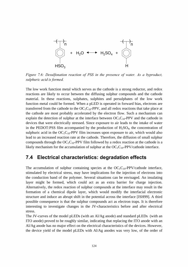
124
HSO3
( )n
H
( )n
H2SO4H2O+ +
Figure 7.6: Desulfonation reaction of PSS in the presence of water. As a byproduct,sulphuric acid is formed.
The low work function metal which serves as the cathode is a strong reductor, and redoxreactions are likely to occur between the diffusing sulphur compounds and the cathodematerial. In these reactions, sulphates, sulphites and persulphates of the low workfunction metal could be formed. When a pLED is operated in forward bias, electrons aretransferred from the cathode to the OC1C10-PPV, and all redox reactions that take place atthe cathode are most probably accelerated by the electron flow. Such a mechanism canexplain the detection of sulphur at the interface between OC1C10-PPV and the cathode indevices that were electrically stressed. Since exposure to air leads to the intake of waterin the PEDOT:PSS film accompanied by the production of H2SO4, the concentration ofsulphuric acid in the OC1C10-PPV film increases upon exposure to air, which would alsolead to an increased reaction rate at the cathode. Therefore, the diffusion of small sulphurcompounds through the OC1C10-PPV film followed by a redox reaction at the cathode is alikely mechanism for the accumulation of sulphur at the OC1C10-PPV/cathode interface.
7.4 Electrical characteristics: degradation effects
The accumulation of sulphur containing species at the OC1C10-PPV/cathode interface,stimulated by electrical stress, may have implications for the injection of electrons intothe conduction band of the polymer. Several situations can be envisaged. An insulatinglayer might be formed, which could act as an extra barrier for charge injection.Alternatively, the redox reaction of sulphur compounds at the interface may result in theformation of a chemical dipole layer, which would modify the interfacial electronicstructure and induce an abrupt shift in the potential across the interface [ISH99]. A thirdpossible consequence is that the sulphur compounds act as electron traps. It is thereforeinteresting to investigate changes in the JV-characteristics before and after electricalstress.The JV-curves of the model pLEDs (with an Al/Ag anode) and standard pLEDs (with anITO anode) proved to be roughly similar, indicating that replacing the ITO anode with anAl/Ag anode has no major effect on the electrical characteristics of the devices. However,the device yield of the model pLEDs with Al/Ag anodes was very low, of the order of
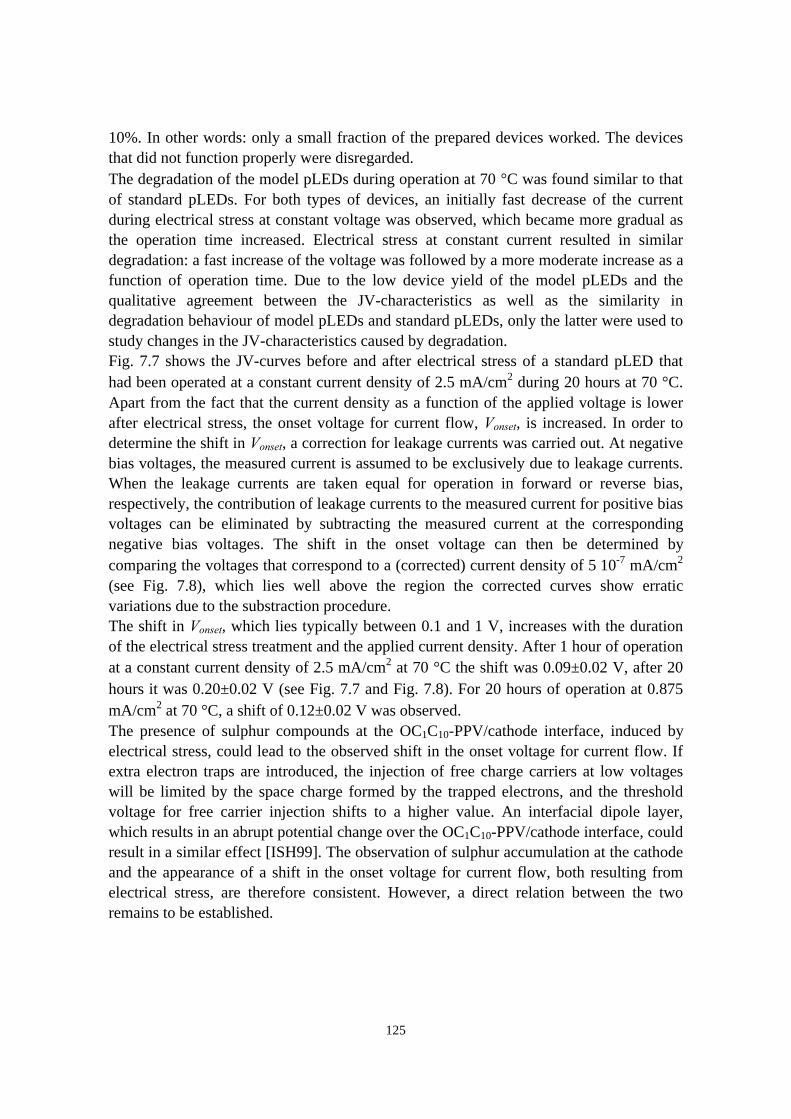
125
10%. In other words: only a small fraction of the prepared devices worked. The devicesthat did not function properly were disregarded.The degradation of the model pLEDs during operation at 70 °C was found similar to thatof standard pLEDs. For both types of devices, an initially fast decrease of the currentduring electrical stress at constant voltage was observed, which became more gradual asthe operation time increased. Electrical stress at constant current resulted in similardegradation: a fast increase of the voltage was followed by a more moderate increase as afunction of operation time. Due to the low device yield of the model pLEDs and thequalitative agreement between the JV-characteristics as well as the similarity indegradation behaviour of model pLEDs and standard pLEDs, only the latter were used tostudy changes in the JV-characteristics caused by degradation.Fig. 7.7 shows the JV-curves before and after electrical stress of a standard pLED thathad been operated at a constant current density of 2.5 mA/cm2 during 20 hours at 70 °C.Apart from the fact that the current density as a function of the applied voltage is lowerafter electrical stress, the onset voltage for current flow, Vonset, is increased. In order todetermine the shift in Vonset, a correction for leakage currents was carried out. At negativebias voltages, the measured current is assumed to be exclusively due to leakage currents.When the leakage currents are taken equal for operation in forward or reverse bias,respectively, the contribution of leakage currents to the measured current for positive biasvoltages can be eliminated by subtracting the measured current at the correspondingnegative bias voltages. The shift in the onset voltage can then be determined bycomparing the voltages that correspond to a (corrected) current density of 5⋅10-7 mA/cm2
(see Fig. 7.8), which lies well above the region the corrected curves show erraticvariations due to the substraction procedure.The shift in Vonset, which lies typically between 0.1 and 1 V, increases with the durationof the electrical stress treatment and the applied current density. After 1 hour of operationat a constant current density of 2.5 mA/cm2 at 70 °C the shift was 0.09±0.02 V, after 20hours it was 0.20±0.02 V (see Fig. 7.7 and Fig. 7.8). For 20 hours of operation at 0.875mA/cm2 at 70 °C, a shift of 0.12±0.02 V was observed.The presence of sulphur compounds at the OC1C10-PPV/cathode interface, induced byelectrical stress, could lead to the observed shift in the onset voltage for current flow. Ifextra electron traps are introduced, the injection of free charge carriers at low voltageswill be limited by the space charge formed by the trapped electrons, and the thresholdvoltage for free carrier injection shifts to a higher value. An interfacial dipole layer,which results in an abrupt potential change over the OC1C10-PPV/cathode interface, couldresult in a similar effect [ISH99]. The observation of sulphur accumulation at the cathodeand the appearance of a shift in the onset voltage for current flow, both resulting fromelectrical stress, are therefore consistent. However, a direct relation between the tworemains to be established.
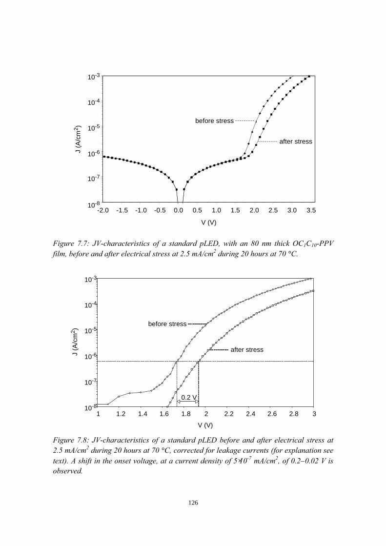
126
-2.0 -1.5 -1.0 -0.5 0.0 0.5 1.0 1.5 2.0 2.5 3.0 3.5
V (V)
10-8
J (A
/cm
2 )
10-7
10-6
10-5
10-4
10-3
before stress
after stress
Figure 7.7: JV-characteristics of a standard pLED, with an 80 nm thick OC1C10-PPVfilm, before and after electrical stress at 2.5 mA/cm2 during 20 hours at 70 °C.
1 1.2 1.4 1.6 1.8 2 2.2 2.4 2.6 2.8 3
V (V)
10-8
J (A
/cm
2)
10-7
10-6
10-5
10-4
10-3
before stress
after stress
0.2 V
Figure 7.8: JV-characteristics of a standard pLED before and after electrical stress at2.5 mA/cm2 during 20 hours at 70 °C, corrected for leakage currents (for explanation seetext). A shift in the onset voltage, at a current density of 5⋅10-7 mA/cm2, of 0.2±0.02 V isobserved.
127
7.5 Discussion and conclusions
The cryogenic RBS measurements on model pLEDs show unequivocally that migrationof sulphur compounds followed by accumulation at the OC1C10-PPV/cathode occurs,stimulated by electrical stress or exposure to air. In both cases, a similar amount ofsulphur atoms was detected at the interface (≈6⋅1014 at./cm2). The results may beexplained by diffusion of small sulphur containing species, followed by a redox reactionat the low work function metal cathode. PEDOT:PSS most probably contains smallamounts of K2S2O8 and H2S2O8, which are retained after the polymerization of EDOT.Additionally, H2SO4 may be formed in the desulfonation of PSS in the presence of water.These molecules could engage in redox reactions with the low work function metal,stimulated by the supply of electrons in case the device is operated in forward bias.Exposure to air results in the intake of water in the PEDOT:PSS film and therefore theproduction of extra H2SO4, which would also accelerate the accumulation of sulphurcontaining species at the cathode. The amount of sulphur atoms that are detected, ≈6⋅1014
at./cm2 which is of the order of a monolayer, might indicate that the redox reactions arelimited by the availability of the low work function metal atoms at the interface.Electrical characterisation of the pLEDs showed that device degradation due to electricalstress resulted in an increase of the onset voltage for current flow. This observation isconsistent with the accumulation of sulphur compounds at the OC1C10-PPV/cathode,since the creation of an interfacial dipole layer or electron traps at the cathode could leadto such an increase. However, caution must be taken in this interpretation of the results,because a direct relation between the two remains to be established. Nevertheless, it hasbeen shown that the interface between PEDOT:PSS and OC1C10-PPV is not stable,resulting in unintentional contamination of the OC1C10-PPV/cathode interface withsulphur compounds.
References
[AND00] G. Andersson, H.H. Brongersma, A.W. Denier van der Gon, L.J. vanIJzendoorn, M.P. de Jong, M.J.A. de Voigt, Synth. Met. 113 (2000) 245
[BER98] A. Berntsen, Y. Croonen, C. Liedenbaum, H. Schoo, R.J. Visser, J.Vleggaar, and P. van de Weijer, Optical Materials 9 (1998) 125
[BRU97] W. Brütting, M.Meier, M. Herold, S. Karg, M. Schwoerer, Chem. Phys.227 (1997) 243
[CAR97] S.A. Carter, M. Angelopoulos, S. Karg, P.J. Brock, and J.C. Scott, Appl.Phys. Lett. 70 (1997) 2067
[DOO85] L.R. Doolittle, Nucl. Instr. and Meth. B 9 (1985) 344[HEW] Hewlett-Packard (www.hp.com), Palo Alto, CA 94304-1185, USA[ISH99] H. Ishii, K. Sugiyama, E. Ito, K. Seki, Adv. Mater. 11 (8) (1999) 605[JON94] F. Jonas, and W. Kraft, US Patent No. 5 300 575 (1994)

128
[KAR97] S. Karg, J.C. Scott, J.R. Salem, and M. Angelopoulos, Synth. Met. 80(1996) 111
[KIM99] J.S. Kim, R.H. Friend, and F. Cacialli, Appl. Phys. Lett. 74 (1999) 3084[SCO96] J.C. Scott, J.H. Kaufman, P.J. Brock, R. DiPietro, J. Salem, and J. A.
Goitia, J. Appl. Phys. 79 (1996) 2745
129
Summary
Semiconducting π-conjugated polymers can be used as the active material in lightemitting diodes (LEDs). Polymer LEDs (pLEDs) are regarded as very promising forcommercial applications: large area devices can easily be obtained, the fabrication offlexible pLEDs is possible due to the unique mechanical properties of polymers, emissionin the entire visible spectrum can be achieved by chemical tuning, and, last but not least,the production costs for pLEDs are relatively low. However, large scale commercialapplication is still hindered by the short lifetime of pLEDs.Interface stability plays an important role in the degradation of pLEDs, which consist of astack of various thin layers (≈100 nm). Using the ion beam analysis techniquesRutherford backscattering spectrometry (RBS) and elastic recoil detection analysis(ERDA), which enable quantitative depth profiling of elements, the various interfaces inpLEDs have been studied during ageing. The applicability of RBS and ERDA to organicsamples like pLEDs however is often limited by ion beam induced damage. Due toenergy deposition by the impinging ions in the polymer film, molecular bonds are brokenand volatile species are formed that escape from the material. The loss of elements limitsthe accuracy of elemental depth profiling and the quantitativity of the measurements.By cooling the samples to cryogenic temperatures, the outgassing of volatile moleculesduring ion irradiation can be strongly reduced. A cryogenic RBS/ERDA setup has beendeveloped, in which the samples are cooled to 10-30 K by means of a Gifford-McMahoncryocooler. A load lock combined with a portable vacuum container enables sampletransfer without exposure to air. A good thermal contact between the sample holder andthe crycooler is achieved by means of a shrink coupling.In cryogenic ERDA measurements with 10 nA 2 MeV He+ beams, the hydrogen loss ratein OC1C10-poly-(phenelynevinylene) (OC1C10-PPV) films is reduced roughly by a factorof ten as compared to room temperature measurements. Chlorine losses in poly-(2-chloroethylacrylate) films are almost completely suppressed in cryogenic RBSmeasurements, which is very promising for depth profiling of chlorine labelledmonomers in polyacrylates. In pLEDs with poly-(3,4-ethylenedioxithiophene): poly-(styrenesulfonate) (PEDOT:PSS) and OC1C10-PPV films covered with an Al cathode,room temperature RBS measurements are virtually impossible due to gas bubbleformation. In cryogenic RBS measurements, this gas bubble formation is effectivelysuppressed.The stability of the interface between ITO and three different semiconducting polymersin pLEDs has been investigated. ITO is by far the most common choice for the anode inpLEDs. In case of sulfonium precursor route PPV on ITO, RBS studies showed thatindium compounds are present in the PPV. These compounds are formed in a chemicalreaction between ITO and HCl, which is released in the thermal conversion of thesulfonium precursor polymer to PPV. Additional annealing increases the concentration of
130
indium compounds. If an Al cathode is present on top of the PPV film, annealing resultsin the accumulation of the indium compounds at the PPV/Al interface.The crucial role played by HCl in the instability of the ITO/PPV interface has beendemonstrated by studies of the interface between ITO and OC1C10-PPV under theinfluence of exposure to HCl vapour. HCl exposure leads to dramatic erosion of the ITO,accompanied by the formation of large (10-100 µm) InCl3 islands in the OC1C10-PPV.By the introduction of an organic hole transport layer, PEDOT:PSS, between the ITOanode and the emissive polymer, the lifetime of pLEDs can be increased significantly.Nevertheless, RBS measurements show that the ITO/PEDOT:PSS interface is not stable:exposure to air leads to erosion of the ITO and the intake of indium compounds in thePEDOT:PSS film, due to the hygroscopic and acidic nature of PSS.Calcium is a suitable cathode material for pLEDs due to its low work function. Theinterface between calcium and the emissive polymer in pLEDs however is very sensitiveto oxidation. For pLEDs of which the Ca cathodes were oxidised in a controlledenvironment, electrical characterisation combined with oxygen depth profiling withERDA shows a clear relation between the amount of oxygen in the pLEDs and the deviceperformance. Exposure of 5-10 nm Ca layers on OC1C10-PPV films to dry oxygen resultsin oxidation of the OC1C10-PPV/Ca interface and device failure. Exposing thicker Calayers to dry oxygen leads to minor oxidation of the Ca cathode and also minordeterioration of the device performance. The incorporation of oxygen in Ca cathodes thatwere deposited in an O2 background pressure can also be correlated to the deviceperformance.As an extension to the cryogenic RBS/ERDA setup, an ERDA time-of-flight (TOF)spectrometer has been developed. By means of ERDA-TOF, accurate separation betweendifferent recoil species is possible and an excellent depth resolution can be achieved. Thespectrometer is operational at present.The stability of the interface between PEDOT:PSS and OC1C10-PPV in pLEDs has beeninvestigated with RBS. Sulphur compounds, originating from the PEDOT:PSS film, werefound to migrate into the OC1C10-PPV and accumulate at the interface between theOC1C10-PPV film and the low work function metal cathode, stimulated by deviceoperation or exposure to air.
131
Samenvatting
Halfgeleidende π-geconjugeerde polymeren kunnen worden gebruikt als het actievemateriaal in light emitterende diodes (LEDs). Polymere LEDs (pLEDs) wordenbeschouwd als veelbelovend voor commerciele toepassingen: devices met een grootoppervlak kunnen gemakkelijk worden gemaakt, de fabricage van flexibele pLEDs ismogelijk dankzij de unieke mechanische eigenschappen van polymeren, emissie in hetgehele zichtbare spectrum kan worden bereikt door chemische tuning, en deproduktiekosten van pLEDs zijn bovendien relatief laag. Het op grote schaal ontwikkelenvan commerciële toepassingen wordt echter vooralsnog bemoeilijkt door de kortelevensduur van pLEDs.Grensvlakstabiliteit speelt een belangrijke rol in de degradatie van pLEDs, die bestaan uiteen aantal opeengestapelde dunne lagen (≈100 nm). Met behulp van deionenbundelanalysetechnieken Rutherford backscattering spectrometry (RBS) en elasticrecoil detection analysis (ERDA), waarmee kwantitatieve diepteprofilering vanelementen mogelijk is, zijn de verschillende grensvlakken in pLEDs bestudeerd tijdensveroudering. De toepasbaarheid van RBS en ERDA op organische preparaten als pLEDswordt echter beperkt door ionenbundelschade. Door de energiedepositie van deinvallende ionen in de polymeerfilm worden moleculaire bindingen verbroken envluchtige moleculen gevormd, die aan het materiaal ontsnappen. Het verlies vanelementen limiteert de nauwkeurigheid van diepteprofilering en de kwantitativiteit van demetingen.Het verlies van vluchtige moleculen tijdens ionenbestraling kan sterk wordengereduceerd door de preparaten te koelen tot cryogene temperaturen. Een cryogeneRBS/ERDA opstelling is ontwikkeld, waarin de preparaten tot 10-30 K worden gekoelddoor middel van een Gifford-McMahon cryokoeler. Een laadsluis gekombineerd met eendraagbare vacuümcontainer maakt het mogelijk om preparaten in te sluizen zonderblootstelling aan lucht. Een goed warmtekontakt tussen de preparaathouder en decryokoeler wordt bereikt door middel van een krimpkoppeling.Het waterstofverlies in OC1C10-poly-(phenelynevinylene) (OC1C10-PPV) lagen tijdenscryogene ERDA metingen met 10 nA 2 MeV He+ bundels wordt met ongeveer een factortien gereduceerd ten opzichte van metingen die bij kamertemperatuur worden uitgevoerd.Het verlies van chloor in poly-(2-chloroethylacrylate) wordt bijna volledig onderdrukt incryogene RBS metingen, hetgeen veelbelovend is voor de diepteprofilering van metchloor gelabelde monomeren. Het verrichten van RBS metingen bij kamertemperatuuraan pLEDs met poly-(3,4-ethylenedioxithiophene):poly-(styrenesulfonate) (PEDOT:PSS)en OC1C10-PPV lagen bedekt met een Al kathode is nagenoeg onmogelijk vanwege devorming van gasbellen. Gasbelvorming wordt effectief onderdrukt in cryogene RBSmetingen.De stabiliteit van het grensvlak tussen ITO en drie verschillende halfgeleidendepolymeren in pLEDs is onderzocht. ITO is verreweg het meest gebruikte anodemateriaal
132
in pLEDs. In het geval van sulfonium precursorroute PPV op ITO hebben RBS studiesaangetoond dat er indiumverbindingen in het PPV aanwezig zijn. Deze verbindingenworden gevormd in een chemische reactie tussen ITO en HCl, hetgeen vrijkomt bij dethermische conversie van het sulfonium precursorpolymeer tot PPV. Extra verhittingresulteert in een toename van de hoeveelheid indiumverbindingen. Indien een Al kathodeop het PPV aanwezig is, zorgt verhitting voor ophoping van de indiumverbindingen aanhet PPV/Al grensvlak.Het belang van de aanwezigheid van HCl voor de instabiliteit van het ITO/PPV grensvlakwordt gedemonstreerd door studies van het grensvlak tussen ITO en OC1C10-PPV, onderinvloed van blootstelling aan HCl damp. Blootstelling aan HCl leidt tot sterke erosie vanhet ITO en de vorming van grote (10-100 µm) InCl3 eilanden in het OC1C10-PPV.Door de introductie van een organische gatentransportlaag, PEDOT:PSS, tussen de ITOanode en het licht uitzendende polymeer kan de levensduur van pLEDs aanzienlijkworden verlengd. Niettemin laten RBS metingen zien dat het ITO/PEDOT:PSS grensvlakniet stabiel is: blootstelling aan lucht leidt tot erosie van het ITO en de opname vanindiumverbindingen in de PEDOT:PSS film, vanwege het hygroscopische en zurekarakter van PSS.Calcium is een geschikt kathodemateriaal voor pLEDs vanwege de lage werkfunctie. Hetgrensvlak tussen calcium en het licht uitzendende polymeer in pLEDs is echter zeergevoelig voor oxidatie. Voor pLEDs waarvan de Ca kathodes in een gecontroleerdeomgeving werden geoxideerd laten elektrische karakterisatie en zuurstofdiepteprofilering met ERDA een duidelijke relatie zien tussen de hoeveelheid zuurstof inde pLEDs en de werking van de devices. Blootstelling van 5-10 nm Ca lagen op OC1C10-PPV films aan droge zuurstof resulteert in oxidatie van het OC1C10-PPV/Ca grensvlak enuitval van de devices. Het blootstellen van dikkere Ca lagen aan droge zuurstof heeftslechts geringe oxidatie van de Ca kathode en een eveneens geringe verslechtering van dedevices tot gevolg. De inbouw van zuurstof in Ca kathodes die in een zuurstofachtergronddruk werden gedeponeerd kan ook met de werking van de devices wordengecorreleerd.De cryogene RBS/ERDA opstelling is uitgebreid met een ERDA time-of-flight (TOF)spectrometer. ERDA-TOF maakt het mogelijk om verschillende recoil deeltjesnauwkeurig te scheiden en bovendien kan een uitstekende diepteresolutie worden bereikt.De spectrometer is op dit moment operationeel.De stabiliteit van het grensvlak tussen PEDOT:PSS en OC1C10-PPV in pLEDs isonderzocht met RBS. Het is aangetoond dat zwavelverbindingen uit het PEDOT:PSS inhet OC1C10-PPV migreren en zich ophopen aan het grensvlak tussen de OC1C10-PPV filmen de kathode, die bestaat uit een metaal met een lage werkfunctie. Dit vindt plaatstijdens werking van de pLEDs en tijdens blootstelling aan lucht.

133
PublicationsA model for ion-irradiation induced hydrogen loss from organic materialsM.P. de Jong, A.J.H. Maas, L.J. van IJzendoorn, S.S. Klein, M.J.A. de VoigtJ. Appl. Phys. 82(3) (1997) 1058
IBA on functional polymersM.P. de Jong, D.P.L. Simons, L.J. van IJzendoorn, M.J.A. de Voigt, M.A. Reijme, A.W. Deniervan der Gon, H.H. BrongersmaProceedings of the Fifteenth International Conference on Applications of Accelerators inResearch and Industry (1998) 447
High energy ion beam analysis on polymers at cryogenic temperaturesM.P. de Jong, L.J. van IJzendoorn, M.J.A. de VoigtNucl. Instr. and Meth. B 161-163 (1999) 207
Indium diffusion in model polymer light-emitting diodesM.P. de Jong, D.P.L. Simons, M.A. Reijme, L.J. van IJzendoorn, A.W. Denier van der Gon,M.J.A. de Voigt, H.H. Brongersma, R.W. GymerSynth. Met. 110 (2000) 1
Analytical techniques with a cyclotron on polymersM.P. de Jong, M.J.A. de Voigt, L.J. van IJzendoorn, H.H. BrongersmaBull. Mater Sci. 22(3) (1999) 687
Stability of the interface between indium-tin-oxide and poly(3,4-ethylenedioxythiophene)/poly(styrenesulfonate) in polymer light-emitting diodesM.P. de Jong, L.J. van IJzendoorn, M.J.A. de Voigtaccepted for publication in Appl. Phys. Lett.
Halogens as trace compounds in polymeric light-emitting diodesG. Andersson, H.H. Brongersma, A.W. Denier van der Gon, L.J. van IJzendoorn, M.P. de Jong,M.J.A. de VoigtSynth. Met. 113 (2000) 245
Formation of indium chloride wires in model polymeric LEDsM.A. Reijme, M.P. de Jong, D.P.L. Simons, M. Schok, A.W. Denier van der Gon, H.H.Brongersma, L.J. van IJzendoorn, M.J.A. de Voigtto be published in J. Appl. Phys.
Influence of the partially oxidized calcium cathode on the performance of polymeric LEDsG.G. Andersson, M.P. de Jong, H.H. Brongersma, A.W. Denier van der Gon, L.J. vanIJzendoorn, M.J.A. de Voigtto be published in Synth. Met.
134
DankwoordAllereerst wil ik mijn 1e promotor, prof. Martien de Voigt, bedanken voor zijnondersteuning gedurende mijn promotieonderzoek. Martien, ik heb tijdens de afgelopenvijf jaar met veel plezier in jouw groep gewerkt, als afstudeerder en als promovendus. Jehebt een belangrijke rol gespeeld in mijn beslissing om te gaan promoveren, waarvan iktot op de dag van vandaag nog geen seconde spijt heb gehad. In de laatste fase heb je jeook erg ingespannen om alles op de valreep rond te krijgen, wat ik erg waardeer. Mijn 2e
promotor, prof. Hidde Brongersma, dank ik voor de nuttige discussies die ik met hem hebgevoerd.Degene die verreweg het meest heeft bijgedragen aan mijn werk is mijn copromotor, Leovan IJzendoorn. Leo, bedankt voor al je steun en enthousiasme. Ik zal onze velebrainstormsessies, die voor een belangrijk deel richting aan mijn werk hebben gegeven,echt missen. Naast een goede begeleider was (en ben) je natuurlijk ook een buitengewoonprettig mens. Bedankt!De door de Gemeenschappelijke Technische Dienst gebouwde cryogeneionenverstrooiingsopstelling vormde de belangrijkste pijler onder mijn werk. Bij hetdenkwerk dat aan het bouwen voorafging speelden Peer Brinkgreve en Erwin Dekkerseen cruciale rol. Het ingenieuze binnenwerk is in elkaar gezet door, met name, Jos deLaat. Ik dank voorgenoemden en de vele anderen van de GTD die hun steentje hebbenbijgedragen voor hun flexibele instelling en de prettige samenwerking. Hoewel ergeruchten gaan dat ik de opstelling nooit heb gebruikt (er ging nooit iets kapot) wil ik diebij deze ontkrachten: hij is gewoon goed gebouwd.Ook Henk Heller heeft een belangrijke bijdrage geleverd aan de bouw van de opstelling.Het ontwerp van het nieuwe deel van de bundellijn en van de ERDA-TOF spectrometerzijn van zijn hand. Ook bij het sleutelen, uitlijnen, etc. heeft Henk mij zeer veel geholpen.Henk, bedankt voor al je hulp. Bij Leo de Folter kon ik ook altijd terecht met technischeproblemen. Leo, bedankt voor je hulp bij van alles en nog wat.Het vervaardigen van de ERDA-TOF spectrometer was in handen van Jan van Asten.Met grote precisie heeft hij alle priegelige componentjes hiervoor gemaakt. Bedankthiervoor.Voor het uitvoeren van de experimenten was het goed functioneren van ons cyclotron eenvereiste. Dankzij Rinus Queens, Frits van Hirtum, Jan van den Berg, Eric van den Eerdenen Wim Kemper was dit geen enkel probleem. Bedankt voor jullie bereidheid om mij tehelpen als er problemen waren. Rinus, nog veel plezier toegewenst met het musiceren ensuccess met het vinden van een opvolger voor mij in de band.Ad Kemper en Harry van Doorn bedank ik voor het bedenken en vervaardigen van debroodnodige elektronica.Een aantal afstudeerders en stagiair(e)s hebben een belangrijke bijdrage aan mijn werkgeleverd: Michiel Schok, Roland Stolk, Twan van Lippen en Silke Schymon. Michielheeft mij in het begin van mijn promotieperiode veel geholpen. De experimenten warenvaak lastig omdat we onze draai nog moesten vinden, en de opstelling waar we toen nog
135
mee werkten werd steeds verder afgebroken omdat er plaats gemaakt moest worden voorde nieuwe cryo-opstelling. Michiel, bedankt dat je toch de moed er in hield enuiteindelijk een goed stuk werk hebt afgeleverd. Roland heeft zich met veel energie enenthousiasme gestort op de degradatieproblematiek van een bepaald soort pLEDs.Hiervoor heeft hij zowel bij Philips Research als op de TUE bergen werk verzet. Bedankthiervoor! Twan heeft onderzoek gedaan aan het mysterieuze PEDOT. Uiteindelijkhebben we toch aardig wat mysteries kunnen ontrafelen. Silke, danke für deine schöneForschungsarbeit nach flüssige Elektroden. Kein Mensch weiβ ob die jemals verwendetwerden, aber wir haben damit spaβ gehabt, oder?Mireille Reijme en Gunther Andersson dank ik voor de prettige samenwerking tijdens devele gezamenlijk uitgevoerde onderzoeksprojecten.Als de computers er geen zin in hadden, was er gelukkig altijd wIm Verseijden om zeweer in het gareel te krijgen. wIm, bedankt. Ook Peter Mutsears wil ik bij deze bedankenvoor zijn hulp, die meestal nodig was als dat eigenzinnige PhyDas systeem onverwachtgedrag vertoonde. Anette Eliëns dank ik voor haar hulp bij administratieve zaken, ook alsik daar weer eens veel te laat mee kwam aanzetten.Mede dankzij mijn (ex-)collega-AIOs heb ik een goede tijd gehad in Eindhoven, op hetwerk en vaak ook ergens anders. Met name wil ik mijn kamergenoten Addo Hammen enLouis Selen bedanken voor het op niveau brengen van de werksfeer. Louis, bedankt ookvoor je gezelschap tijdens onze reis door de States en succes met het afronden van jepromotie. David Simons bedank ik voor de succesvolle gezamenlijke projecten en degezellige tijd in Siena. Zonder namen te noemen dank ik ook al mijn overige (ex-)collegas voor de vier goede jaren.Door toeval is mijn broer, Arthur de Jong, wetenschappelijk medewerker geworden in degroep waar ik mijn promotieonderzoek verrichte. Art, bedankt voor alles, ook voor deberoepsmatige hulp.Het in vier jaar afronden van een promotieonderzoek is natuurlijk alleen mogelijk metsteun van de mensen uit je privèleven. Nelly en Joop, bedankt voor alles. Martina,bedankt voor al je begrip en liefdevolle ondersteuning, vooral tijdens de laatsteafmattende maanden. Wir haben es geschaft!
136
Curriculum Vitae
16 juli 1970 Geboren te 's-Hertogenbosch
1982-1988 Atheneum B aan het Jeroen Bosch College te 's-Hertogenbosch
1988-1992 Studie Technische Natuurkunde aan de Technische HogeschoolEindhoven
1992-1996 Verkorte studie Technische Natuurkunde aan de Technische UniversiteitEindhoven
1996-2000 Promotieonderzoek aan de Technische Universiteit Eindhoven in de groepToepassingen van Ionenbundels van de faculteit Technische Natuurkunde
sept. 2000- Post-doctoraal onderzoeker aan de Universiteit van Linköping (Zweden)in de groep Surface Physics and Chemistry
Stellingen
behorende bij het proefschrift
Interface stability in polymer light emittingdiodes
A study with cryogenic ion beam techniques
door
Michel de Jong
17 oktober 2000
-I-De toepasbaarheid van hoge energie ionenverstrooiingstechnieken op organischepreparaten kan aanzienlijk worden vergroot door gebruik te maken van een gekoeldepreparaathouder.
Dit proefschrift
-II-Voor het bestuderen van de gevolgen van oxidatie van calcium cathodes in polymerelicht emitterende diodes is het van wezenlijk belang dat zowel de fabricage van dedevices als de oxidatie onder zo goed mogelijk gecontroleerde omstandighedenplaatsvinden.
Dit proefschrift, hoofdstuk 5
-III-De instabiliteit van het grensvlak tussen indium-tin-oxide (ITO) en poly-(3,4-ethyleendioxythiofeen):polystyreensulfonaat) (PEDOT:PSS), veroorzaakt doorblootstelling aan lucht, kan de strengere eis voor inkapseling van polymere lichtemitterende diodes met ITO/PEDOT:PSS anodes ten opzichte van devices met ITOanodes verklaren.
Dit proefschrift, hoofdstuk 4 en A. Berntsen et al., Opt. Mater. 9 (1998) 125
-IV-Bij de keuze van een elektrodemateriaal voor polymere licht emitterende diodes dientmen zich te realiseren dat niet alleen de werkfunctie van het elektrodemateriaal bepalendis voor de injectie van ladingsdragers in het polymeer, maar met name ook deeigenschappen van het elektrode/polymeer grensvlak.
-V-Het door middel van koeling tegengaan van het verlies van vluchtige componenten uitorganische preparaten tijdens RBS en ERDA metingen is alleen succesvol indien de doorde ionenbundel gedeponeerde warmte ook effectief kan worden afgevoerd.
-VI-De werking en levensduur van polymere licht emitterende diodes met indium-tin-oxide(ITO) anodes kunnen sterk worden verbeterd door een zuurstofplasmabehandeling vanhet ITO, zelfs wanneer een organische gatentransportlaag op het ITO is aangebracht.
zie bijvoorbeeld: J.S. Kim et al., Appl. Phys. Lett. 74 (1999) 3084

-VII-De door Whitlow berekende doorgangstijd voor elektronen in electrostatic mirror timingdetectors is meer dan een factor vier te groot, waardoor ten onrechte wordt gesuggereerddat variaties in de lengte van de door de elektronen doorlopen banen in die detectoren eenbelangrijke bijdrage leveren aan de onzekerheid in de vluchtijdmetingen in ERDA-TOFexperimenten.
H.J. Whitlow et al., Nucl. Instr. and Meth. A310 (1991) 636
-VIII-In tegenspraak met het door Adel ontwikkelde model voor waterstofverlies in organischematerialen wordt tijdens bestraling met hoog energetische ionen geen stabielewaterstofconcentratie bereikt.
M.E. Adel et al., J. Appl. Phys. 66 (1989) 3248
-IX-De door een windturbine en een kerncentrale jaarlijks geproduceerde hoeveelhedenenergie per eenheid gebruikt aardoppervlak zijn bij benadering gelijk.
-X-De maan lijkt vlak boven de horizon groter te zijn dan hoog aan de hemel, hetgeen nietberust op fysische verschijnselen maar op gezichtsbedrog.
-XI-Van een goedkope, stug afgestelde gitaar kan met behulp van een nagelvijl een goedbespeelbaar instrument worden gemaakt.
-XII-Het is opvallend dat in het liedje "Getting Better" dat wordt gebruikt in dereclamecampagne van Philips, met als motto "Let's make things better", de zin: "can't getno worse" voorkomt.
"Getting Better", door Paul McCartney en John Lennon