Interface investigation and engineering - Yang Yang Lab
24
Interface investigation and engineering – achieving high performance polymer photovoltaic devices†‡ Li-Min Chen,x a Zheng Xu,x b Ziruo Hong a and Yang Yang a Received 2nd December 2009, Accepted 12th January 2010 First published as an Advance Article on the web 26th February 2010 DOI: 10.1039/b925382c The contact between the polymer active layer and the electrode is one the most critical interfaces in polymer solar cells. In this article, we report the progress of interface engineering in polymer solar cell research, where the multiple functions of the interfacial materials will be discussed. The vertical composition profile in polymer:fullerene blends is an emerging topic, and the interlayer effect on the vertical phase separation and device performance will be highlighted. We also discuss the energy level alignment at the bulk heterojunction (BHJ) interface, with the aim of providing a better understanding towards the route of high efficiency polymer solar cells. 1. Introduction Recent progress in polymer photovoltaics, has led to reports of power conversion efficiencies (PCEs) reaching 6–7%. 1–5 In addi- tion, the scalability and compatibility with flexible, large-area substrates affirms polymer solar cells for high throughput, low cost renewable energy alternatives to their inorganic counter- parts. The advancement of record-high PCEs is driven by the synthesis of novel donor and acceptor materials, implementation of innovative interfacial materials, and adoption of revolutionary processing conditions. In the bulk heterojunctions (BHJs), the inevitable potential loss due to the energy level offset between the donor and acceptor renders the electrode contacts a critical factor to derive the net potential out of the BHJs. It is therefore necessary to establish ohmic contacts at both electrodes for efficient charge extraction, which is challenging for interfaces between organic/polymer and metals. An interface with a barrier height of a few tens of mV may result in significant charge accumulation, and thus significant recombination loss and infe- rior photovoltaic (PV) performance. Consequently, the interface between the BHJ and both the anode and cathode is of funda- mental importance to the charge transport and extraction process, which determines the device performance and long term stability. Tremendous efforts have been devoted to elucidate and engineer the interface since the evolution of polymer solar cells. Particularly in solution-processed polymer active layers, the surface properties of the bottom interface have a substantial influence on the film morphology, while the BHJ morphology grown above can be manipulated accordingly. In this article, we shall highlight common interfacial materials employed at the anode and cathode of polymer solar cells. An overview of the functional interlayers will be provided. Both the a Department of Materials Science and Engineering, University of California, Los Angeles, Los Angeles, CA 90095, USA b Solarmer Energy, Inc., 3445 Fletcher Ave, El Monte, CA 91731, USA † This paper is part of a themed issue of Journal of Materials Chemistry on Interface engineering of organic and molecular electronics, guest edited by Alex Jen. ‡ The authors gratefully acknowledge financial support from the Air Force Office of Scientific Research (Grant No. FA9550-07-1-0264), Office of Naval Research (Grant No. N00014-04-1-0434), Solarmer Energy Inc., University of California Discovery Grant, and NSF IGERT: Materials Creation Training Program (MCTP) (DGE-0114443) and the California Nano-Systems Institute (CNSI). x Contributed equally to this work. Li-Min Chen Li-Min (Raymond) Chen has been a Ph.D. student in Prof. Yang Yang’s group in the Department of Materials Science and Engineering at the University of California, Los Angeles since 2006. He obtained his B.S. and M.S. from National Cheng Kung University (Tai- wan) in 2002 and 2004, respec- tively. His research focuses on polymer solar cells with novel structures and processing methods as well as transparent conductor applications. Zheng Xu Zheng Xu is a Senior Researcher at Solarmer Energy, Inc. in El Monte, CA. He obtained his Ph.D. in Materials Science and Engineering at the University of California, Los Angeles in 2009, focusing on organic electronic devices and their interfaces (advisor: Prof. Yang Yang). Before he entered UCLA, he received his B.S. (2000) and M.S. (2003) in Physics at Fudan University (China). His current research focus is on polymer solar cells. This journal is ª The Royal Society of Chemistry 2010 J. Mater. Chem., 2010, 20, 2575–2598 | 2575 FEATURE ARTICLE www.rsc.org/materials | Journal of Materials Chemistry
Transcript of Interface investigation and engineering - Yang Yang Lab

FEATURE ARTICLE www.rsc.org/materials | Journal of Materials Chemistry
Interface investigation and engineering – achieving high performance polymerphotovoltaic devices†‡
Li-Min Chen,xa Zheng Xu,xb Ziruo Honga and Yang Yanga
Received 2nd December 2009, Accepted 12th January 2010
First published as an Advance Article on the web 26th February 2010
DOI: 10.1039/b925382c
The contact between the polymer active layer and the electrode is one the most critical interfaces in
polymer solar cells. In this article, we report the progress of interface engineering in polymer solar cell
research, where the multiple functions of the interfacial materials will be discussed. The vertical
composition profile in polymer:fullerene blends is an emerging topic, and the interlayer effect on the
vertical phase separation and device performance will be highlighted. We also discuss the energy level
alignment at the bulk heterojunction (BHJ) interface, with the aim of providing a better understanding
towards the route of high efficiency polymer solar cells.
1. Introduction
Recent progress in polymer photovoltaics, has led to reports of
power conversion efficiencies (PCEs) reaching 6–7%.1–5 In addi-
tion, the scalability and compatibility with flexible, large-area
substrates affirms polymer solar cells for high throughput, low
cost renewable energy alternatives to their inorganic counter-
parts. The advancement of record-high PCEs is driven by the
synthesis of novel donor and acceptor materials, implementation
of innovative interfacial materials, and adoption of
aDepartment of Materials Science and Engineering, University ofCalifornia, Los Angeles, Los Angeles, CA 90095, USAbSolarmer Energy, Inc., 3445 Fletcher Ave, El Monte, CA 91731, USA
† This paper is part of a themed issue of Journal of Materials Chemistryon Interface engineering of organic and molecular electronics, guestedited by Alex Jen.
‡ The authors gratefully acknowledge financial support from the AirForce Office of Scientific Research (Grant No. FA9550-07-1-0264),Office of Naval Research (Grant No. N00014-04-1-0434), SolarmerEnergy Inc., University of California Discovery Grant, and NSFIGERT: Materials Creation Training Program (MCTP)(DGE-0114443) and the California Nano-Systems Institute (CNSI).
x Contributed equally to this work.
Li-Min Chen
Li-Min (Raymond) Chen has
been a Ph.D. student in Prof.
Yang Yang’s group in the
Department of Materials
Science and Engineering at the
University of California, Los
Angeles since 2006. He obtained
his B.S. and M.S. from National
Cheng Kung University (Tai-
wan) in 2002 and 2004, respec-
tively. His research focuses on
polymer solar cells with novel
structures and processing
methods as well as transparent
conductor applications.
This journal is ª The Royal Society of Chemistry 2010
revolutionary processing conditions. In the bulk heterojunctions
(BHJs), the inevitable potential loss due to the energy level offset
between the donor and acceptor renders the electrode contacts
a critical factor to derive the net potential out of the BHJs. It is
therefore necessary to establish ohmic contacts at both electrodes
for efficient charge extraction, which is challenging for interfaces
between organic/polymer and metals. An interface with a barrier
height of a few tens of mV may result in significant charge
accumulation, and thus significant recombination loss and infe-
rior photovoltaic (PV) performance. Consequently, the interface
between the BHJ and both the anode and cathode is of funda-
mental importance to the charge transport and extraction
process, which determines the device performance and long term
stability. Tremendous efforts have been devoted to elucidate and
engineer the interface since the evolution of polymer solar cells.
Particularly in solution-processed polymer active layers, the
surface properties of the bottom interface have a substantial
influence on the film morphology, while the BHJ morphology
grown above can be manipulated accordingly.
In this article, we shall highlight common interfacial materials
employed at the anode and cathode of polymer solar cells. An
overview of the functional interlayers will be provided. Both the
Zheng Xu
Zheng Xu is a Senior
Researcher at Solarmer Energy,
Inc. in El Monte, CA. He
obtained his Ph.D. in Materials
Science and Engineering at the
University of California, Los
Angeles in 2009, focusing on
organic electronic devices and
their interfaces (advisor: Prof.
Yang Yang). Before he entered
UCLA, he received his B.S.
(2000) and M.S. (2003) in
Physics at Fudan University
(China). His current research
focus is on polymer solar cells.
J. Mater. Chem., 2010, 20, 2575–2598 | 2575

Fig. 1 Schematic variation of VOC with the acceptor strength (VOC1)
and/or electrode work function (VOC2) in a BHJ solar cell device.
(Reprinted with permission from ref. 7; copyright 2003, American
Institute of Physics.)
lateral and vertical phase morphologies are critical to the device
performance, but only recently has the vertical phase
morphology acquired immense attention. The vertical phase
morphology is essential to the charge transport and collection
process since the photoactive layer is sandwiched between the
two electrodes. We will discuss the effect of the interface property
on the film morphology, mainly in the vertical direction, and
report methods on controlling the vertical composition gradient.
The last part will focus on the energy alignment at the BHJ/
electrode interfaces.
2. Interfacial materials
2.1 Functions of interfacial materials
The metal/organic interface plays an essential role in determining
the overall device performance of organic electronics, and
inserting a functional interfacial layer can dramatically alter the
interface properties. The main functions of the interfacial layer
include:
(1) Minimization of the energy barrier for charge injection and
extraction. In OLED/PLEDs, the injection efficiency of carriers
dramatically depends on the barrier height at the metal/organic
interface, where the tunneling current is inversely proportional to
the barrier height.6 In this sense, it is intuitive to lower the barrier
height by engineering the interface contacts. In polymer solar
cells, it is rather important to understand whether the open-
circuit voltage (VOC), which relates to the built-in electric field for
charge extraction, is determined by the intrinsic properties of the
BHJ system (VOC1), or the choice of metal electrodes (VOC2), as
illustrated in Fig. 1.7 For non-ohmic contacts, the VOC follows
the metal–insulator–metal (MIM) model, which equals the work
function difference of the electrodes. On the other hand, charge
transfer leads to the Fermi level alignment for ohmic contacts,
and the work function of the cathode and anode is pinned to the
lowest unoccupied molecular orbital (LUMO) of the acceptor
and the highest occupied molecular orbital (HOMO) of the
donor, respectively, determining the VOC. In this case, band
Ziruo Hong
Ziruo Hong obtained his B.S. in
Chemistry from Sichuan
University, 1995, and Ph.D. in
physics from Changchun Insti-
tute of Optics, Fine Mechanics
and Physics, Chinese Academy
of Sciences in 2001. He has been
working on device design and
mechanism study of organic
electroluminescence and photo-
voltaics in Hong Kong, Singa-
pore and Germany. He is
currently working on polymer
solar cells, especially solar cells
with stacking structures, in Prof.
Yang Yang’s group at UCLA. His main research interest is focused
on organic opto-electronics, especially light emitting devices and
photovoltaic cells. He has published over 70 research papers on
international journals.
2576 | J. Mater. Chem., 2010, 20, 2575–2598
bending at the ohmic contact reduces the VOC (Fig. 2), whereas
charge recombination at the donor/acceptor interface governs
the VOC of the BHJ device.8–12 More recently, the formation of
charge transfer excitons (CTEs) between the polymer and
fullerene has shown strong correlation with the VOC, providing
insight to its origin, as well as suggested routes to approach the
theoretical VOC.11,13–16
(2) Formation of a selective contact for single types of charge
carrier. Charge selectivity at the electrode interfaces is crucial to
ensure effective charge extraction by blocking the charge carrier
flow towards the unfavored direction. Interfacial layers of wide
bandgaps can serve as an exciton-blocking layer (EBL) to elim-
inate the parasitic exciton quenching at the metal/organic inter-
face.17–20 Furthermore, certain interfacial layers allow the
selective transportation of either electrons or holes, such as an
electron-transporting layer (ETL) with hole-blocking properties,
and a hole-transporting layer (HTL) with electron-blocking
properties. These functional interfacial layers can significantly
improve the charge selectivity at the electrodes,21–23 and have been
widely implemented in OLED/PLEDs, and excellent reviews
can be found in the articles by Hung and Chen24 and Walzer
et al.25
Yang Yang
Originally from Taiwan, Prof.
Yang received his Ph.D. degree
in Physics and Applied Physics
at the University of Massachu-
setts, Lowell. After working at
the University of California,
Riverside as a postdoctoral
researcher, and in the UNIAX
Corporation as a research staff
member, he joined the Univer-
sity of California, Los Angeles
in 1997. He has been a full
professor at UCLA since 2002.
His group is working on solution
processable electronic devices,
including organic and inorganic solar cells, organic LED and
memory devices, and carbon-based nanomaterials. He has pub-
lished more than 170 articles in peer-reviewed journals.
This journal is ª The Royal Society of Chemistry 2010

Fig. 2 Schematic band diagram of a metal–insulator–metal (MIM)
device with (a) non-ohmic and (b) ohmic contacts for electrons and holes.
Before (upper image) and after contact (lower image) under short-circuit
conditions. 4b and DVb are the injection barrier height for electrons at
a non-ohmic contact and the voltage loss at an ohmic contact, respectively.
4M1 and 4M2 are work functions of the metal contacts. (Reprinted with
permission from ref. 7; copyright 2003, American Institute of Physics.)
(3) Determination of the relative polarity of the devices. In
principle, ITO is capable of collecting either electrons or holes
since its work function (ca. 4.5–4.7 eV) lies between the typical
HOMO and LUMO of common organic photovoltaic (OPV)
materials. Accordingly, the polarity of ITO can be modified to
efficiently collect either electrons or holes by coating with func-
tional interlayers of different work functions.26 Device polarity is
thus controlled by the relative positions of functional interlayers
with various work functions, irrespective of the conducting
electrodes, as shown in Fig. 3. Metals with various work func-
tions can also be employed as either cathode or anode via
selecting suitable interlayers. The versatility of ITO establishes
the foundation of the inverted structure solar cell, which also
exhibits the potential advantage of improved lifetime and
preferred vertical composition gradient.27–29
(4) Modification of the surface property to alter film
morphology. The substrate surface property is capable of
manipulating the film morphology due to the surface-directed
Fig. 3 The device structure of a polymer solar cell, where the device
polarity can be controlled by the relative position of the functional buffer
layers. (Reprinted with permission from ref. 26; copyright 2006, Amer-
ican Institute of Physics.)
This journal is ª The Royal Society of Chemistry 2010
spinodal decomposition, particularly during the spin-coating
process of the polymer blend films.30–32 Modifying the substrate
surface property with various self-assembled monolayers
(SAMs) can alter the molecular preference and arrangement at
the film/substrate interface, and therefore affect the contact
properties, such as barrier height and available charge transfer
sites, as well as the vertical phase morphology.28,29,33,34
(5) Suppression of diffusion and reaction between the electrode
material and polymer. A detrimental effect of metal ion diffusion
into the organic layer is substantial leakage current.35,36 The
chemical reaction at the metal/organic interface can also vary the
contact properties, forming interfacial dipole barriers and defect
states that pin the Fermi level. The kink/hump (s-shape) observed
in certain current density–voltage (J–V) curves is speculated to
arise from the interface barriers.37,38 Therefore, an inert buffer layer
that prevents the diffusion and reaction at this interface is desired.
(6) Modulation of the optical field as an optical spacer. The BHJ
active layer is typically sandwiched between two electrodes, where
one is transparent and the other reflective. The incident light
forms a standing wave inside the active layer. The optical field
intensity diminishes to zero at the polymer/reflecting electrode
interface, while the maximum intensity is located at a certain
distance away from the reflective mirror, depending on the
refractive indices and thickness of the active layer. An optically
transparent spacer can redistribute the electric field and push the
absorbing region away from the interface to a higher electric-field
strength, which enhances the short-circuit current (JSC), as shown
in Fig. 4.4,39,40 Optical spacers have been shown to be most
effective for thin active layers limited by low carrier mobilities,
whilst not so useful for films of optimal film thickness.41,42
2.2 Overview of interfacial materials
In the last twenty years extensive efforts have been devoted to
OLED/PLED research and a variety of functional interfacial
Fig. 4 (a) Schematic representation of the spatial distribution of the
squared optical electric-field strength |E|2 inside the devices with a struc-
ture of ITO/PEDOT/active layer/Al (left) and ITO/PEDOT/active layer/
optical spacer/Al (right). (b) The current density–voltage characteristics
of polymer solar cells with ( ) and without (-) the TiOx optical spacer
under AM 1.5 illumination. (Reprinted with permission from ref. 39;
copyright 2006, Wiley VCH.)
J. Mater. Chem., 2010, 20, 2575–2598 | 2577

materials have been developed,24 and also successfully trans-
ferred to engineer the interfaces in polymer solar cells with
promising results. This article will provide an overview of the
most prominent interfacial materials in polymer solar cell
applications. The interfacial materials implemented at both the
cathode and anode interfaces will be separately discussed within
three main categories, namely inorganic salts, inorganic semi-
conducting oxides, and organic and self-assembled monolayers
(SAMs).
2.2.1 Cathode interlayers. It is preferable for the cathode
interface to have a low work function contact for efficient elec-
tron extraction. While Al and Ag are the most common electrode
materials, the thermal evaporation process frequently alters the
quality of the metal/organic interface.43,44 The reactive hot metal
atoms can lead to chemical interaction at the interface and
diffusion into the organic layer.45,46 It should be noted that
alternative approaches are also capable for the cathode deposi-
tion, such as spray-coating of Ag nanoparticles and transferring
of Ag nanowire meshes.47,48 L€ogdlund et al.49 and Antoniadis
et al.50 suggested that the instability of the Al electrode is related
to the Al–C bond formation, which interrupts the p-conjugated
system. Therefore, other low work function metals such as Ca,
Mg, and Ba, are often employed to protect the metal/organic
interface, while being capped by the Al or Ag electrode.
The low work function metal Ca has been used to
improve device performance since the development of
polymer diodes.1,51,52 For poly(3-hexylthiophene):[6,6]-phenyl-
C61-butyric acid methyl ester (P3HT:PCBM) blend-based solar
cells with an Al cathode, a dipole layer pointing from Al to
PCBM exists at the PCBM/Al interface, which increases the
charge extraction barrier and reduces the VOC.7,53 Inserting Ca
between the Al electrode and the polymer forms an ohmic
contact that results in a high fill factor (FF).54 The thin n-doped
layer induced by Ca deposition pins the surface energy level at
the polymer/metal interface, which facilitates the charge trans-
port.55 Ca reacts with water at room temperature, while being
relatively inert to molecular oxygen.56 Nonetheless, the instabil-
ities of Ca and Mg in ambient atmosphere require combining
with metals with a low permeation rate to moisture such as Al
and Ag to form effective cathodes. In a recent study, low work
function bilayer electrodes such as Ba/Al and Ca/Al show
superior device performance than higher work function
electrodes (Table 1).57
Table 1 Detailed current density–voltage (J–V) characteristics forvarious top electrodes. Literature work function (F) values are listed forthe metal contacting the active metal. (Reprinted from ref. 57; copyright2008, American Institute of Physics)
Electrode
Workfunction(eV)
VOC
(mV)JSC
(mA/cm2) FF (%)Normalizedefficiency
Ag 4.26 403 � 27 9.04 � 1.16 36.6 � 3.7 0.36 � 0.08Al 4.28 420 � 15 10.02 � 0.33 38.2 � 2.6 0.41 � 0.03Mg:Ag/Ag 3.66 565 � 6 10.30 � 0.39 50.5 � 2.8 0.75 � 0.06LiF/Al 2.9 580 � 2 10.42 � 0.22 57.3 � 1.2 0.89 � 0.03Ca/Al 2.87 601 � 2 10.42 � 0.18 60.6 � 2.1 0.96 � 0.04Ba/Al 2.7 600 � 2 10.47 � 0.36 62.2 � 1.5 1.00 � 0.04
2578 | J. Mater. Chem., 2010, 20, 2575–2598
Alkali metal compounds, including LiF,58–60 CsF,61 Cs2CO3,62–64
CsCl,65 as well as 8-hydroxyquinolinolato lithium (Liq)66 and
other organic metal complexes,67 typically provide low work
function contacts, and are commonly used as the electron
injection layer in OLED/PLEDs. Alkali metal acetates also
deliver similar results.68 Among these functional compounds,
LiF and Cs2CO3 have found the most success in polymer solar
cells.
The introduction of a bilayer cathode composed of LiF/Al and
MgO/Al can enhance electron injection due to band bending of
the organic layer in contact with the insulating layers.58 By
inserting LiF or other compounds (oxides and halides) of group
IA and IIA metals between Al and tris-8-hydroxyquinoline
aluminium (Alq3), a better contact is also formed.69,70 LiF was
adapted to polymer solar cells to facilitate electron extraction,
and resulted in significant device improvement for the poly-
(2-methoxy-5-(30,70-dimethyl-octyloxy))-p-phenylene vinylene
(MDMO-PPV):PCBM blend, where the VOC and FF increased
to 0.82 V and 61%, respectively.71 The function of the LiF layer
was suggested to arise from either dipole formation at the
Al/LiF/polymer interface70,72 or the LiF buffer protection.73
J€onsson et al. reported the thickness-dependence of LiF, where
for (sub)monolayer coverage, Al deposition decomposes LiF,
causing Li-doping of the organic material to yield a low work
function contact,74 while thicker LiF creates a dipole layer that
downshifts the work function.75 Other fluorides such as CsF,61
CaF2,69 MgF2,76 NaF,77 and KF,78,79 were also reported to
exhibit similar phenomena. A comparative study between LiF,
NaF, and KF showed that the variation in reverse current
density is caused not only by interface modification but also by
diffusion and doping of the whole organic layer, which depends
on the interlayer thickness.80 NaF was suggested as an alternative
choice due to the minimum thickness requirement.
Caesium carbonate (Cs2CO3) is another promising electron
injection material.62–64,81,82 The function of Cs2CO3 is rather
versatile and insensitive to the cathode material, where thermal
evaporation or spin-coating the Cs2CO3 layer, as well as using
either Al or Ag as the electrode, deliver comparable perfor-
mances.82 The actual product of thermally-evaporated Cs2CO3,
either doped caesium oxide or caesium carbonate molecules, has
been under debate.82–87 Nonetheless, the formation of a low work
function Al–O–Cs complex upon Al deposition facilitates elec-
tron extraction in polymer solar cells and electron injection in
PLEDs.82 Inserting a 1 nm Cs2CO3 layer between the active layer
and the Al increases both the VOC and FF.26 Chen et al. reported
similar results with improvement to 3.1% PCE due to the reduced
series resistance (Rs).88 A 2.1% PCE semitransparent polymer
solar cell was also fabricated with a 70% transparency cathode
composed of Cs2CO3 (1 nm)/Ag (7 nm)/ITO (100 nm). The
device performance was further improved to 2.8% by placing
a reflective Ag mirror behind the device to compensate for light
loss.89 While 0.5 �A of Cs2CO3 is sufficient to lower the electron
injection barrier into Alq3, a minimum thickness of 10 �A is
required to convert the ITO surface to a low work function
cathode for the inverted structure.85 Modification of the ITO
polarity for inverted structure and their performance will be
discussed in the next section.
Transparent semiconducting metal oxides such as TiO2 are
commonly employed as an electron acceptor and transport
This journal is ª The Royal Society of Chemistry 2010

material because of its processability and non-toxicity, as well as
wide applications in dye sensitized solar cells and
photocatalysts.90–92 TiO2 is a robust diffusion barrier against
oxygen and water due to its scavenging effects originating from
photocatalysis and oxygen deficiency.90,93 Relatively air-stable
polymer solar cells and LEDs have been demonstrated by
incorporating the TiOx layer.94 Fig. 5 illustrates a device struc-
ture incorporating the TiOx layer, as well as how this layer
prevents the permeation of oxygen and moisture. The flow chart
also shows the preparation steps of the TiOx layer.
Generally, crystalline TiO2, either in the anatase or rutile
phase, requires a heat treatment process above 450 �C that is
incompatible with polymer devices. For the practical use of low
cost polymer PV devices, it is essential to fabricate functional
oxide layers with compatible solution processes. Kim et al.
reported a low temperature sol–gel process to fabricate a tita-
nium oxide layer (Fig. 5).39 A spin-coated precursor solution
converts to a 30 nm titanium oxide film by hydrolysis in air at
room temperature, and a transparent amorphous titanium oxide
film was obtained after annealing at 150 �C for 10 min. XPS
study revealed an oxygen-deficient TiOx film, where
Ti:O ¼ 1:1.34. The TiOx film exhibited an electron mobility
approximately 1.7 � 10�4 cm2 V�1 s�1, and a LUMO level of
4.4 eV, close to the work function of Al, rendering it an efficient
electron-transport material. The large band gap of the TiOx film
(ca. 3.7 eV) is capable of blocking the holes and excitons
efficiently. In addition, the TiOx layer serves as an optical spacer
to spatially redistribute the light intensity inside the device
(Fig. 4a).4,39,40,95 The TiOx optical spacer substantially enhances
both the external quantum efficiency (EQE) and JSC (Fig. 4b) by
approximately 40% compared to devices without the optical
spacer and a 5% PCE was achieved in P3HT:PCBM BHJ devices.
Hayakawa et al. also reported substantial device enhancement
for a TiOx layer atop the active layer, but with only a small
Fig. 5 The device architecture with the TiOx layer, as ITO/PEDOT:PSS/
active layer/TiOx/Al. The TiOx layer functions as a scavenging layer to
block the permeation of oxygen and moisture into the polymer active
layer. The brief flow chart shows the preparation steps of the TiOx.
(Reprinted with permission from ref. 94; copyright 2007, Wiley VCH.)
This journal is ª The Royal Society of Chemistry 2010
increase in JSC.22 Due to the excellent hole-blocking property of
TiOx, the enhancement in shunt resistance (Rsh) and rectification
ratio contributed to the improvement in both VOC and FF, while
the TiOx layer also functions as a barrier against physical
damage and chemical degradation. Recently, a 6.1% PCE was
reported for poly[N-900-hepta-decanyl-2,7-carbazole-alt-5,5-
(40,70-di-2-thienyl-20,10,30-benzothiadiazole):[6,6]-phenyl C71-
butyric acid methyl ester (PCDTBT:PC70BM) BHJ device by
inserting a TiOx layer, with an internal quantum efficiency (IQE)
approaching 100% around 450 nm.4 Such a high IQE value
indicates the high efficiency of converting absorbed photons into
charge carriers that are collected at the electrodes. However, in
the case of additive incorporation, the optical spacer effect
counteracts with the additive concentration, i.e. the nanoscale
roughness.95
Incorporation of dopants and varying processing are common
methods to modify the metal oxide properties.96–98 We reported
Cs-doped TiO2 (TiO2:Cs) by mixing Cs2CO3 solution with
a nanocrystalline TiO2 solution synthesized via a non-hydrolytic
sol–gel process.99 Cs lowers the TiO2 work function such that the
TiO2:Cs interfacial layer improves the polymer/metal contact, as
well as provides excellent electron extraction and hole-blocking
properties to deliver a PCE of 4.2%. The versatile functionality of
the TiO2:Cs layer was also extended to PLEDs with similar
improvement. Fig. 6 shows that the TiO2:Cs interfacial layer
delivers better performance compared to either TiO2 or Cs2CO3
alone in both PV devices and PLEDs.
Solution-process high efficiency polymer tandem cells using
TiOx and poly(3,4-ethylenedioxythiophene):poly(styrene
Fig. 6 (a) Current density–voltage characteristics of a P3HT:PC70BM
BHJ device with an evaporated Al cathode and different interfacial
layers. (b) Current density–voltage–brightness characteristics for a PLED
device with different interfacial layers. (Reprinted with permission from
ref. 99; copyright 2009, Wiley VCH.)
J. Mater. Chem., 2010, 20, 2575–2598 | 2579

sulfonate) (PEDOT:PSS) as the interlayer were successfully
demonstrated with a 6.5% PCE.100 The TiOx layer functions as
the electron transport and collecting layer for the front sub-cell
as well as the foundation of the rear sub-cell, where the
PEDOT:PSS layer serves as the hole-transport layer (HTL). We
also reported implementing pristine TiO2 and TiO2:Cs in a tandem
cell based on P3HT:PC70BM and poly[(4,40-bis(2-ethyl-
hexyl)dithieno[3,2-b:20,30-d]silole)-2,6-diyl-alt-(2,1,3-benzothiadiazole)-
4,7-diyl] (PSBTBT):PC70BM BHJs, with a PCE of 5.84%.101,102
The TiO2/PEDOT:PSS (4083) interconnecting layer behaves as
a Schottky contact, where exposure to UV light increases the free
carrier concentration in TiO2 which leads to efficient electron
tunneling through the energy barrier.103 Fig. 7a shows the
necessity of UV light illumination to the TiO2 layer, where
a significant hump (s-shape) was observed with the UV cutoff
filter. It was also pointed out that extra care should be taken to
avoid under-estimating the device area when using high
conductivity materials in the interlayer, such as PH500 (Fig. 7b).
Another solution-processable n-type metal oxide is ZnO,
which has a high electron mobility of 0.066 cm2 V�1 s�1.104 ZnO
also shows a similar optical spacer effect for thin active layers,
which is less pronounced for thick films.41 This indicates that the
optical spacer effect might be particularly advantageous for thin
films limited by low carrier mobilities, but not for films of
optimal film thickness.39,42 The first polymer tandem cell using
a solution-processed interlayer was realized with a combination
of ZnO nanoparticles and neutral PEDOT.105 Neutral PEDOT
was used since acidic PEDOT dissolves the ZnO nanoparticles.
Fig. 7 (a) Current density–voltage characteristics of single and tandem
cells under illumination with and without a 400 nm cutoff filter. (b)
A tandem cell using PH500 as an interlayer before and after defining the
active area by scratching. (Reprinted with permission from ref. 102;
copyright 2009, Wiley VCH.)
2580 | J. Mater. Chem., 2010, 20, 2575–2598
The charge recombination at the interlayer was improved by
n-doping (photo-doping) the ZnO layer by exposure to UV
light,106,107 where incorporating metallic clusters also exhibits
similar effects.108
Modifying the ITO surface with SAMs with permanent dipole
moments can alter the work function and surface property to
improve the device performance. SAMs with electron with-
drawing groups increases the ITO work function, while electron
donating groups reduce it.109 However, the resulting phase
separation was reported to be a more dominating factor than
matching the energy levels. Khodabakhsh et al. utilized SAMs to
improve both hole injection and charge collection, pointing out
that SAM-modified electrodes can affect the subsequent film
morphology and the density of active sites for charge collec-
tion.33,110 SAMs can also be used in combination with functional
metal oxides, such as TiO2 and ZnO, to further improve the
interface properties. Systematic studies of modifying the TiO2/
BHJ interface showed that SAMs can improve the interface via
several mechanisms, including: reducing charge recombination,
passivating inorganic surface states, providing additional exciton
dissociation interface, and influencing the BHJ composition
distribution for better charge selectivity.111,112 Alkanethiol SAMs
were shown to increase the JSC for hybrid P3HT-ZnO solar cells
from 0.28 to 0.42 mA/cm2 despite their insulating nature. The
enhanced JSC was due to the increased crystallinity of the inter-
facial P3HT, which can be attributed to larger exciton diffusion
length, hole mobility, or reduced electron–hole recombination
rate.113–115 Interface modification with SAMs of different dipole
directions and chemical bondings can significantly improve the
contact properties of the ZnO/metal bilayer cathode, where
stable high work function metals, such as Ag and Au, can also be
used as cathodes.116,117 Modifying the ZnO surface with a benzoic
acid (BA) group decorated with a negative dipole (such as
–OCH3 or –CH3 end groups), which points toward the ZnO layer
(away from the metal), decreases the band offset and facilitates
the ohmic contact formation. A cathode with a ZnO/BA–OCH3/
Al configuration exhibited a 4.2% PCE compared to 3.2% from
the unmodified cathode. Modification of the ZnO with a mer-
captoundecanoic acid (MUA) SAM further improved the
efficiency to 4.6%.116
Reports on organic interfacial material in polymer solar cells
have been scarce, despite their wide application in OLEDs and
small molecule solar cells.25 Poly(ethylene oxide) (PEO) was
shown to enhance the VOC up to 200 mV, possessing the similar
function as LiF, but with the advantage of solution process-
ability.118 Ionic liquid-functionalized carbon nanoparticles
(ILCNs) play a similar role to lower the electron collection
barrier at the cathode.119 A thin layer of alcohol/water-soluble
polyelectrolyte can improve the VOC up to 0.3 V due to super-
position of the interfacial dipole upon the built-in electric field.120
Alcohol-soluble polyfluorene derivatives as the cathode buffer
layers also show similar device performance improvement.121,122
2.2.2 Anode interlayer. PEDOT:PSS has been commonly
used to improve the anode contact with ITO.123 Spray deposition
of a thick PEDOT:PSS layer (ca. 1.2 mm) as the top electrode has
been demonstrated with a PCE of 2%.124 However, its acidic
nature etches the ITO and imposes potential lifetime insta-
bility.125–127 Rutherford backscattering (RBS) studies showed
This journal is ª The Royal Society of Chemistry 2010
that the ITO/PEDOT:PSS interface is not stable, where indium
diffuses into the PEDOT:PSS. XPS also confirmed the dissolu-
tion of ITO in PEDOT:PSS. Furthermore, previous studies
revealed PEDOT:PSS to be an inefficient electron-blocking layer
due to electron leakage at the anode.126,128
Two criteria must be taken into consideration for an efficient
anodic buffer layer to replace PEDOT:PSS. The fabrication
compatibility must be guaranteed to withstand the organic
solvent exposure. Furthermore, the surface properties of the
anodic buffer layer have a significant impact on the molecular
ordering and phase separation process of the BHJ active layer,
which must be considered as well. A few transition metal oxides
(MoO3, V2O5, and WO3) are highly transparent and conductive,
and have been successfully employed to modify the anode
interface. In addition to replacing PEDOT:PSS for the ITO/
polymer contact, these transition metal oxides have particularly
found applications in the inverted structure polymer solar cells,
since they can be easily evaporated on top of the polymer active
layer. We will first discuss the hole collection properties of these
transition metal oxides in the regular device structure, followed
by their applications in the inverted structure.
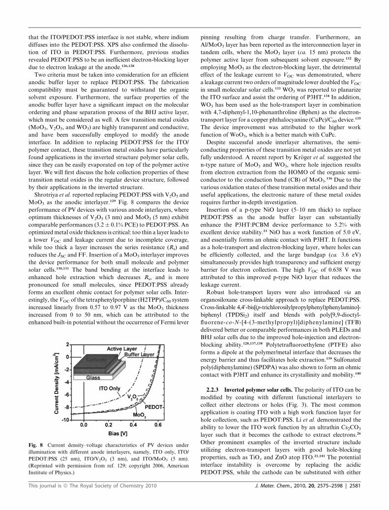
Shrotriya et al. reported replacing PEDOT:PSS with V2O5 and
MoO3 as the anodic interlayer.129 Fig. 8 compares the device
performance of PV devices with various anode interlayers, where
optimum thicknesses of V2O5 (3 nm) and MoO3 (5 nm) exhibit
comparable performances (3.2� 0.1% PCE) to PEDOT:PSS. An
optimized metal oxide thickness is critical: too thin a layer leads to
a lower VOC and leakage current due to incomplete coverage,
while too thick a layer increases the series resistance (Rs) and
reduces the JSC and FF. Insertion of a MoO3 interlayer improves
the device performance for both small molecule and polymer
solar cells.130,131 The band bending at the interface leads to
enhanced hole extraction which decreases Rs, and is more
pronounced for small molecules, since PEDOT:PSS already
forms an excellent ohmic contact for polymer solar cells. Inter-
estingly, the VOC of the tetraphenylporphine (H2TPP)/C60 system
increased linearly from 0.57 to 0.97 V as the MoO3 thickness
increased from 0 to 50 nm, which can be attributed to the
enhanced built-in potential without the occurrence of Fermi lever
Fig. 8 Current density–voltage characteristics of PV devices under
illumination with different anode interlayers, namely, ITO only, ITO/
PEDOT:PSS (25 nm), ITO/V2O5 (3 nm), and ITO/MoO3 (5 nm).
(Reprinted with permission from ref. 129; copyright 2006, American
Institute of Physics.)
This journal is ª The Royal Society of Chemistry 2010
pinning resulting from charge transfer. Furthermore, an
Al/MoO3 layer has been reported as the interconnection layer in
tandem cells, where the MoO3 layer (ca. 15 nm) protects the
polymer active layer from subsequent solvent exposure.132 By
employing MoO3 as the electron-blocking layer, the detrimental
effect of the leakage current to VOC was demonstrated, where
a leakage current two orders of magnitude lower doubled the VOC
in small molecular solar cells.133 WO3 was reported to planarize
the ITO surface and assist the ordering of P3HT.134 In addition,
WO3 has been used as the hole-transport layer in combination
with 4,7-diphenyl-1,10-phenanthroline (Bphen) as the electron-
transport layer for a copper phthalocyanine (CuPc)/C60 device.135
The device improvement was attributed to the higher work
function of WoO3, which is a better match with CuPc.
Despite successful anode interlayer alternatives, the semi-
conducting properties of these transition metal oxides are not yet
fully understood. A recent report by Kr€oger et al. suggested the
n-type nature of MoO3 and WO3, where hole injection results
from electron extraction from the HOMO of the organic semi-
conductor to the conduction band (CB) of MoO3.136 Due to the
various oxidation states of these transition metal oxides and their
useful applications, the electronic nature of these metal oxides
requires further in-depth investigation.
Insertion of a p-type NiO layer (5–10 nm thick) to replace
PEDOT:PSS as the anode buffer layer can substantially
enhance the P3HT:PCBM device performance to 5.2% with
excellent device stability.23 NiO has a work function of 5.0 eV,
and essentially forms an ohmic contact with P3HT. It functions
as a hole-transport and electron-blocking layer, where holes can
be efficiently collected, and the large bandgap (ca. 3.6 eV)
simultaneously provides high transparency and sufficient energy
barrier for electron collection. The high VOC of 0.638 V was
attributed to this improved p-type NiO layer that reduces the
leakage current.
Robust hole-transport layers were also introduced via an
organosiloxane cross-linkable approach to replace PEDOT:PSS.
Cross-linkable 4,40-bis[(p-trichlorosilylpropylphenyl)phenylamino]-
biphenyl (TPDSi2) itself and blends with poly[9,9-dioctyl-
fluorene-co-N-[4-(3-methylpropyl)]diphenylamine] (TFB)
delivered better or comparable performances in both PLEDs and
BHJ solar cells due to the improved hole-injection and electron-
blocking ability.128,137,138 Polytetrafluoroethylene (PTFE) also
forms a dipole at the polymer/metal interface that decreases the
energy barrier and thus facilitates hole extraction.139 Sulfonated
poly(diphenylamine) (SPDPA) was also shown to form an ohmic
contact with P3HT and enhance its crystallinity and mobility.140
2.2.3 Inverted polymer solar cells. The polarity of ITO can be
modified by coating with different functional interlayers to
collect either electrons or holes (Fig. 3). The most common
application is coating ITO with a high work function layer for
hole collection, such as PEDOT:PSS. Li et al. demonstrated the
ability to lower the ITO work function by an ultrathin Cs2CO3
layer such that it becomes the cathode to extract electrons.26
Other prominent examples of the inverted structure include
utilizing electron-transport layers with good hole-blocking
properties, such as TiOx and ZnO atop ITO.21,141 The potential
interface instability is overcome by replacing the acidic
PEDOT:PSS, while the cathode can be substituted with either
J. Mater. Chem., 2010, 20, 2575–2598 | 2581

Fig. 9 Device efficiency and contact angle with water of the Cs2CO3
interlayer as a function of different annealing temperatures. The inset
shows the effect of annealing treatment on the EQE. Line I is the Cs2CO3
layer without annealing, and line II is after 150 �C annealing. (Reprinted
with permission from ref. 87; copyright 2008, American Institute of
Physics.)
Fig. 10 (a) Variation of secondary electron edge with different buffer
layers on ITO, (b) scheme for the formation of dipole layer on ITO and its
effect on reducing the ITO work function. (Reprinted with permission
from ref. 152; copyright 2008, Wiley VCH.)
PEDOT:PSS, which has excellent oxygen-blocking properties,142
or other high work function materials.
Using a solution-processed titanium oxide of 10 nm as the
electron-selective contact and PEDOT:PSS/Au as the anode
delivered an inverted cell of 3.1% PCE.21 The PEDOT:PSS
solution was diluted in isopropanol and heated to 80 �C prior to
spin-coating upon the hydrophobic polymer active layer. The
reduced leakage current under reversed bias indicates the effec-
tive hole-blocking property of the TiOx layer. o-Xylene instead of
chlorobenzene (CB) was used as the solvent and the formation of
a favorable morphology with improved vertical phase separation
was suggested.143 Polyoxyethylene tridecyl ether (PTE) improved
the TiOx precursor wetting to form a better contact, which results
in a higher FF due to reduced Rs and increased Rsh.144 Ameri
et al. compared the regular and inverted structure by optical
modeling, and attributed the higher EQE maximum of the
inverted structure to the non-negligible absorption of the
PEDOT:PSS layer.145 However, no significant ‘‘optical spacer’’
effect of the TiOx layer was observed in the inverted structure.
Incorporating ZnO on ITO as the cathode buffer layer with
a silver anode delivers a PCE of 2.58%.141 An almost 85% EQE
maximum validates the excellent IQE and charge collection
efficiency. Kyaw et al. fabricated inverted cells based on ZnO and
MoO3 interlayers.146 The ZnO transmittance was controlled by
the crystal size, which depends on the precursor concentration.147
Relatively stable solar cells with a 3.5% PCE were obtained by
using ZnO nanoparticles to modify the ITO substrate.27 Modi-
fying the ZnO nanoparticle surface with a C60-SAM further
improved the efficiency to 4.9%. The C60-SAM passivates the
surface traps of ZnO, and enhances the electronic coupling at the
ZnO/organic interface, which suppresses the recombination los-
ses. It was speculated that PCBM accumulation at the C60-SAM
interface benefits the high PCE since organic field effect tran-
sistor (OFET) measurements showed the accumulation of
PCBM at the C60-SAM-modified interface.111
An ultrathin Ca layer was also used as the electron-transport
layer to modify the ITO, while an optimum thickness of MoO3
served as the hole-transporting layer to prevent charge recom-
bination at the Ag anode.148 Interestingly, transition from
regular to inverted device was reported due to oxidation of the
silver top contact, where the work function changes from 4.3 to
5.0 eV upon oxidation.149
Vanadium oxide has various oxidation states and is reported
to protect the polymer active layer and suppress the backward
current at the PCBM/metal interface, as well as to prevent
penetration of the hot metal atoms.36,150 A 2.25% PCE inverted
cell was fabricated by modifying the ITO surface with Cs2CO3,
with V2O5/Al as the anode.26 Semitransparent inverted devices
were formed by replacing Al with 12 nm of Au. The PCE
increased to 4.2% by annealing the Cs2CO3 layer at 150 �C for 20
min, which was attributed to the heavily-doped caesium oxide
formation that reduces the interfacial resistance at the cathode.87
Fig. 9 shows that the device performance increases with the
annealing temperature of the Cs2CO3 layer until 150 �C, which
also corresponds to the variation in contact angle of the Cs2CO3-
modified surface with water. The inset shows the significant
enhancement upon annealing at 150 �C. The improvement is also
due to the beneficial vertical composition profile of the inverted
structure, which will be discussed in the next section.28,29
2582 | J. Mater. Chem., 2010, 20, 2575–2598
Ouyang and Yang reported that by incorporating D-sorbitol
into PEDOT:PSS, a transparent ‘‘electric glue’’ can be formed,
which is capable of laminating films together both mechanically
and electrically.151 Implementing the unique property of the
electric glue into the inverted configuration, a semitransparent
polymer solar cell based on the P3HT:PCBM blend was fabri-
cated by the lamination process with a 3% PCE.152 This method
took advantage of the solution process, which also featured self-
encapsulation and provided an alternative to the roll-to-roll
production. A series of alkali metal compounds were evaluated,
and revealed the formation of interface dipole layers at the ITO
surface, which is shown in Fig. 10. The direction of the dipole
moments points from the ITO surface to vacuum that reduces the
This journal is ª The Royal Society of Chemistry 2010

ITO work function. The amount of the work function reduction
is determined by the magnitude of the dipole moment, which
correlates to the VOC variation, and is proportional to the elec-
tron-donating ability of the alkali metal ions.
In order to fabricate transparent top electrodes, either thermal
evaporation of very thin metal layers or sputter deposition of
transparent metal oxides are required.26,89,153–156 However, thin
metal layers often suffer from transparency loss and low
conductivity, while sputter deposition inevitably introduces
damage to the polymer layer.155,157 The inverted structure based
on Cs2CO3 allows the formation of transparent cathodes, such as
Cs2CO3/Ag/ITO, which was deposited on flexible metal foils and
yielded a ca. 3% PCE.158 Evidently, another application of
transition metal oxides lies in protecting the polymer active layer
during the sputtering process to form a semitransparent elec-
trode, such as MoO3/ITO.159 Other examples include MoO3/Ag/
MoO3, WO3/Ag/WO3, MoO3/Al, which are employed in tandem
or multiple-stacked cells.132,153,160
An ordered heterojunction that utilizes the ordered meso-
porous architecture of inorganic materials possesses the advan-
tage of controlled nanoscale phase separation, and defined
pathways without dead ends to provide straightforward charge
collection.161 Coakley and McGehee demonstrated hybrid
P3HT-titania ordered BHJ devices with a 0.5% PCE. Since then,
nanotube arrays of TiO2 and ZnO have been implemented to
assist the charge transport for P3HT:PCBM blends in inverted
cells, but the performance was still inferior to most regular device
structures.150,162–164 The typical small pore sizes of 10–20 nm are
comparable to the exciton diffusion lengths of polymers, but
result in rather random polymer chain packing instead of the
high degree of p–p stacking.165 The efficiency is thus limited by
the poor alignment (crystallinity), low mobility, and insufficient
infiltration of the polymer. Recently, Mor et al.166 demonstrated
a 4.1% PCE double heterojunction polymer solar cell via verti-
cally oriented TiO2 nanotube arrays, as illustrated in Fig. 11. By
tailoring the pore sizes of the TiO2 nanotubes, the infiltrated
polymer chains self-aligned into aggregates according to the
nanotube direction. It has been reported that the hole mobility
can be enhanced 20 times by this vertical channel confinement-
Fig. 11 Illustration of the double heterojunction polymer solar cells
based on TiO2 nanotube arrays. (Reprinted with permission from ref.
166; copyright 2007, American Institute of Physics.)
This journal is ª The Royal Society of Chemistry 2010
induced alignment.165 Moreover, both polymer-fullerene and
polymer-TiO2 interfaces provided efficient charge separation,
and the nanotube arrays prohibited charge recombination at the
electrodes since simultaneous contact with both electrodes can be
avoided. This double heterojunction device exhibited an EQE
maximum of 80%, and a high JSC of 12.4 mA/cm2.
3. Vertical phase separation
3.1 Vertical phase separation in polymer blends
The film morphology evolution of polymer blends is a complex
interplay governed by the phase-separation process and the
interaction between the polymer components and the surface and
substrate interface, where the final morphology is controlled by
both thermodynamic and kinetic parameters. The rapid evapo-
ration of the solvent freezes the film morphology into a non-
equilibrium state, whereas relaxation toward the equilibrium
state is often prohibited by kinetic barriers. Due to the low
entropy of mixing, immiscible polymer blends tend to demix
(phase-separate) upon spin-coating from their parent blend
solutions, while surface effects and differences in surface energies
have profound effects on the composition profile.167 Surface
properties have long been known to significantly impact the
phase-separation morphology in binary polymer blends, while
blend composition, polymer–substrate interaction, and interfa-
cial tension all play crucial roles in determining the final film
morphology.168
Theoretically, the composition in polymer blend films can be
described as characteristic wave vectors qk and qt, which are
parallel and normal to the substrate, respectively. When 1/qt is
comparable to the film thickness, vertical phase separation can
be promoted by increasing qt from attracting one of the blend
components to the surface via modifying the chemical structures
or substrate properties.30,169 Indeed, vertical-segregated blend
films due to preferred interaction with the air interface and
a more viscous solvent have been reported.170 In this section,
vertical phase separation in conventional and conjugated poly-
mer blends will be introduced, as well as their applications in
polymer electronics. The observations of vertical phase separa-
tion in two major polymer solar cell systems will be discussed,
along with the utilization of this concept.
Experimentally probing the composition of polymer blend
films was made possible by advances in depth profiling and
imaging techniques. A comprehensive review can be referred to
the article by Krausch.171 Depth profiling techniques include
forward recoil spectrometry (FReS) and nuclear reaction anal-
ysis (NRA), which are based on real space profiling, and neutron
reflectivity (NR) and X-ray reflectivity (XRR), which are based
on momentum space. Jones et al. showed experimentally surface-
directed spinodal decomposition of a mixture of isotopic
polymer poly(ethylenepropylene) (PEP) and perdeuterated
poly(ethylenepropylene) (d-PEP), where preferential attraction
leads to enrichment of d-PEP at the surface.30 Fig. 12 shows that
the surface is enriched with d-PEP, and a damped oscillation
from the surface, the wavelength of which grows with the
annealing time. Bruder and Brenn reported that the surface
interaction can alter the spinodal decomposition process to form
either a bilayer morphology or domain structures.172 Krausch
J. Mater. Chem., 2010, 20, 2575–2598 | 2583

Fig. 12 Volume fraction vs. depth profiles of d-PEP in an initially
uniform mixture with a d-PEP volume fraction of 0.5 after aging at 35 �C
for (a) 19 200 s, (b) 64 440 s, and (c) 172 800 s. (Reprinted with permis-
sion from ref. 30; copyright 1991, The American Physical Society.)
Fig. 13 A schematic model describing the film formation during the
spin-coating process, and the final film morphology. (a) After the initial
spin-off stage where both polymer and solvent are removed (i), (ii), the
film separates into two layers (iii) and the film thins owing to solvent
evaporation only. The interface between the polymers destabilizes (iv)
and the film phase-separates laterally (v), (vi). (b) An atomic force
microscope image of the final morphology. (Reprinted with permission
from ref. 175; copyright 2005, Nature Publishing Group.)
et al. studied the thickness dependence of the spinodal decom-
position process to the film composition, revealing interference
effects from the two spinodal waves originating from the two
distinct surfaces.31 Walheim et al. revealed that the topography
of polymer blend films is controlled by the solvent solubility and
the substrate properties.32 By properly tailoring these two
parameters, either component in the immiscible polystyrene/
poly(methyl methacrylate) (PS/PMMA) blend can be preferen-
tially segregated at the substrate surface, where the film
morphology can also show a complete phase inversion. Ton-
That et al. reported surface enrichment of PMMA in various
compositions of the PS/PMMA blend, and attributed the surface
segregation to the different solubility of the polymers in the
solvent and the relative dewetting of PMMA-rich domains from
PS-rich phases.173 Budkowski et al. demonstrated that the
solvent evaporation rate depends on the substrate surface
chemistry, which changes the convection process.168 Concave
and convex surface features were observed for blend films of
polystyrene (PS) and polyisoprene (PI) spin-coated from toluene
onto hydrophobic and hydrophilic SAM-modified substrates,
respectively, while the overall morphology was similar. B€oltau
et al. showed that the phase-separated domains can form
2584 | J. Mater. Chem., 2010, 20, 2575–2598
arbitrary structures with a concentration variation by patterning
the surface with various SAMs.174 Morphology evolution was
studied in situ by time-resolved small-angle light scattering and
light reflectivity.175 The formation of the transient wetting layers
at both the surface and substrate interfaces initiates from the
vertical stratification, and the heterogeneous solvent evaporation
causes a solvent concentration gradient, which leads to the
interfacial (Marangoni-like) instability and eventually lateral
phase separation. This film evolution process in spin-coating is
illustrated in Fig. 13. Depending on the spin-coating parameters,
the initial multilayer structures can either be ‘‘frozen’’168 or
‘‘broken up’’176 into lateral domains. Arias et al. also reported
that by controlling the solvent evaporation rate, either self-
stratified or lateral phase separated morphologies could be
obtained.177
Besides conventional polymer blend systems, vertical phase
separation has also been reported on a variety of semiconducting
polymer systems, which possess important applications in
organic electronics, such as LEDs and transistors. Chappell et al.
utilized scanning near-field optical microscopy (SNOM) to
identify the poly(9,90-dioctylfluorene) (PFO) emission from the
poly(9,90-dioctylfluorene-altbenzothi-adiazole) (F8BT)-rich
domains originating from the preferential wetting of the PFO
This journal is ª The Royal Society of Chemistry 2010

film (ca. 10 nm) at the surface.178 Kim et al. studied the film
morphology of (F8BT) and poly(2,7-(9,9-di-n-octylfluorene)-alt-
(1,4-phenylene-((4-secbutylphenyl)imino)-1,4-phenylene)) (TFB)
blend.179 An enrichment of the low surface energy component
(TFB) at both the air and substrate interfaces was observed as
a result of interfacial-energy reduction. Due to the preferential
wetting of the hole-transporting TFB layer at the substrate,
PLEDs without a PEDOT:PSS layer with comparable efficiency
were demonstrated. Higgins et al. reported the existence of
a wetting layer for different composition ratio, and pointed out
that a better solvent can impede its formation.180 Both the
composition ratio and the casting solvent have a significant effect
on the PLED device performances, and different stages of the
film morphology evolution can thus be obtained by controlling
the solvent evaporation rate via substrate heating.181,182
Vertical segregation was also reported in P3HT blended with
other semicrystalline polymers.183 The sequential crystallization
induced vertical stratification to occur in a ‘‘double-percolation-
like’’ mechanism.184 The film morphology results from successive
phase separation processes, initially in the liquid phase, followed
by segregation of the solidified P3HT, which is caused by the
crystallization of the matrix component. The exothermic crys-
tallization process drives the solidified semiconducting polymer
to segregate toward the surface and interface, leading to a verti-
cally phase-separated morphology. These vertically-stratified
structures are particularly beneficial for FET applications, since
transport of charge carriers only takes place at the gate dielectrics
interface.185 Utilizing this concept, only 3 wt% semiconducting
polymer was required without compromising the performance.
By varying the substrate surface energy, PMMA can either
segregate at the top surface to function as an encapsulation
material or at the bottom surface as a dielectric layer.186,187
Furthermore, the PSS-rich surface in the PEDOT:PSS blend has
been identified,188,189 while adding glycerol or D-sorbitol to the
PEDOT:PSS solution prior to spin-coating increases the film
conductivity due to aggregation of PEDOT-rich particles.151,190
Fig. 14 Schematic illustration of the solar cells with active layers based
on APFO-3 and PCBM with: (A) diffuse bilayer morphology, (B)
spontaneously formed multilayer structure, and (C) homogenous blend
morphology. (D) The corresponding J–V characteristics under white
light illumination for the 3 device morphologies. (Reprinted with
permission from ref. 195; copyright 2009, Wiley VCH.)
3.2 Vertical phase separation in APFO-3:PCBM
The vertical phase separation plays a crucial role in the charge
collection process of polymer solar cells, since the photo-
generated charges must transport vertically to the sandwiching
electrodes. Two polymer blend systems, namely polyfluorene and
polythiophenes, blended with PCBM, have received considerable
investigation regarding the vertical phase separation morphology
to date.
Alternating polyfluorene copolymers (APFOs), with various
donor–acceptor–donor segments, have been intensively studied
for photoactive materials and achieved a PCE of 4.2%.191,192
J€onsson et al. reported surface enrichment of poly[(9,9-dioctyl-
fluorenyl-2,7-diyl)-co-5,5-(40,70-di-2-thienyl-20,10,30-benzothia-
diazole] (APFO-3), where the surface composition for a 1:4 blend
ratio of APFO-3:PCBM was 1:1.75 Dynamic secondary ion mass
spectroscopy (SIMS) is an established technique to map the
topographic and compositional profiles in both lateral and
vertical directions, thus revealing the 3D morphology of polymer
blend films.193 Bj€orstr€om et al. utilized dynamic SIMS and
observed a multilayer structure after spin-coating APFO-
3:PCBM blends in chloroform for a range of blend ratios.194 The
This journal is ª The Royal Society of Chemistry 2010
vertical structure exhibited a four-fold multilayer morphology
with APFO-3 enriched at the surface, followed by a PCBM-
enriched layer underneath, then an APFO-3-enriched layer in the
middle, and a PCBM-enriched (APFO-3-depleted) layer adjacent
to the substrate. It was suggested that the self-stratification was
due to composition waves caused by the surface-directed phase
separation,30 and if enough time was allowed to reach thermo-
dynamic equilibrium, a bilayer structure instead of the frozen
four-layer structure should eventually evolve. Recently,
Bj€orstr€om et al. compared the photovoltaic performance of the
APFO-3:PCBM blend of three various device structures:
a vertically homogeneous layer, a diffusive bilayer, and a spon-
taneously formed multilayer, as illustrated in Fig. 14A–C.195 The
diffusive bilayer was formed by spin-coating PCBM dissolved in
dichloromethane solution at high speed onto the polymer layer,
whereas APFO-3 was partially dissolved by exposure to
dichloromethane.196,197 By selecting a solvent with a desired
volatility (evaporation rate), homogeneous or multilayer
J. Mater. Chem., 2010, 20, 2575–2598 | 2585
structures can be formed by spin-coating from chlorobenzene
(CB)198 and chloroform, respectively.194 It has been reported that
a homogeneous film is favored by slow evaporation and weak
polymer–PCBM interaction, while rapid solvent evaporation
and strong polymer–PCBM interaction leads to a lateral film
structure. Interestingly, the multilayer structure shows the best
performance of 3.5% PCE, with a higher JSC and FF (Fig. 14D),
despite excess hole-transporting material (APFO-3) accumu-
lating at the cathode. The improved performance can be attrib-
uted to this functional structure that can favorably absorb
photons and dissociate excitons at distinct regions, as well as the
beneficial effect of PCBM content on charge mobilities compared
to a homogeneous blend.199–201 Efficient electron transport
through a polymer-rich ‘‘skin’’ layer has been reported in
MDMO-PPV:PCBM blends.202 This result indicates that further
investigation is required to correlate the engineering of the
vertical morphology to the resulting device performance. Specific
interactions of the blend component with the substrate, such as
the interaction between the thiophene groups and gold, might
pose an additional factor on the vertical morphology, especially
in the vicinity of the substrate.203
3.3 Vertical phase separation in P3HT:PCBM
Vertical phase separation in the P3HT:PCBM system has been
reported by several groups through various analysis techniques.
Though the precise vertical composition profile is still under
debate, the experimental results are discussed here for compar-
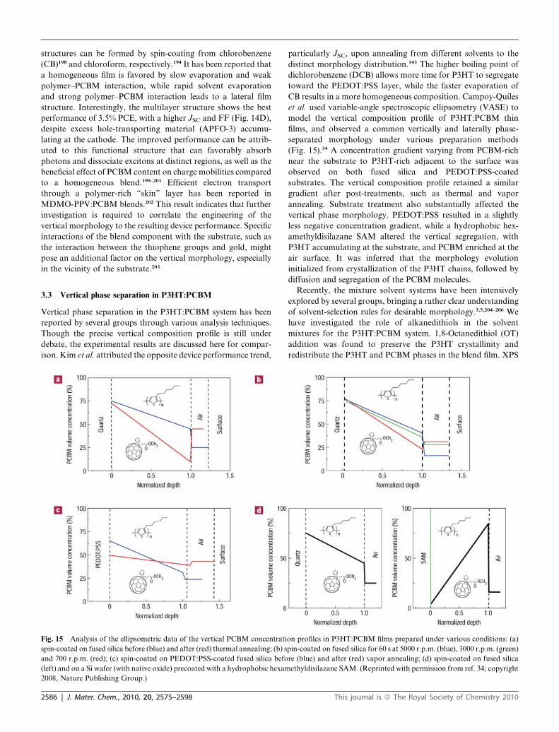
ison. Kim et al. attributed the opposite device performance trend,
Fig. 15 Analysis of the ellipsometric data of the vertical PCBM concentrati
spin-coated on fused silica before (blue) and after (red) thermal annealing; (b) s
and 700 r.p.m. (red); (c) spin-coated on PEDOT:PSS-coated fused silica befo
(left) and on a Si wafer (with native oxide) precoated with a hydrophobic hexam
2008, Nature Publishing Group.)
2586 | J. Mater. Chem., 2010, 20, 2575–2598
particularly JSC, upon annealing from different solvents to the
distinct morphology distribution.143 The higher boiling point of
dichlorobenzene (DCB) allows more time for P3HT to segregate
toward the PEDOT:PSS layer, while the faster evaporation of
CB results in a more homogeneous composition. Campoy-Quiles
et al. used variable-angle spectroscopic ellipsometry (VASE) to
model the vertical composition profile of P3HT:PCBM thin
films, and observed a common vertically and laterally phase-
separated morphology under various preparation methods
(Fig. 15).34 A concentration gradient varying from PCBM-rich
near the substrate to P3HT-rich adjacent to the surface was
observed on both fused silica and PEDOT:PSS-coated
substrates. The vertical composition profile retained a similar
gradient after post-treatments, such as thermal and vapor
annealing. Substrate treatment also substantially affected the
vertical phase morphology. PEDOT:PSS resulted in a slightly
less negative concentration gradient, while a hydrophobic hex-
amethyldisilazane SAM altered the vertical segregation, with
P3HT accumulating at the substrate, and PCBM enriched at the
air surface. It was inferred that the morphology evolution
initialized from crystallization of the P3HT chains, followed by
diffusion and segregation of the PCBM molecules.
Recently, the mixture solvent systems have been intensively
explored by several groups, bringing a rather clear understanding
of solvent-selection rules for desirable morphology.3,5,204–206 We
have investigated the role of alkanedithiols in the solvent
mixtures for the P3HT:PCBM system. 1,8-Octanedithiol (OT)
addition was found to preserve the P3HT crystallinity and
redistribute the P3HT and PCBM phases in the blend film. XPS
on profiles in P3HT:PCBM films prepared under various conditions: (a)
pin-coated on fused silica for 60 s at 5000 r.p.m. (blue), 3000 r.p.m. (green)
re (blue) and after (red) vapor annealing; (d) spin-coated on fused silica
ethyldisilazane SAM. (Reprinted with permission from ref. 34; copyright
This journal is ª The Royal Society of Chemistry 2010

Fig. 16 Proposed model of film evolution during the spin-coating
process. Black wire: P3HT polymer chain; large black dots: PCBM; blue
dots: DCB molecules; and red dots: OT molecules. (a–c) correspond
to three stages in the spin-coating process when DCB is the sole solvent;
(d–f) correspond to three stages in the spin-coating process when OT is
added to the DCB. Note the difference of PCBM distribution in the final
stage of each case, (c) and (f). (Reprinted with permission from ref. 206;
copyright 2008, Wiley-VCH.)
Fig. 17 Schematic of the inverted configuration and the vertical phase
separation of the P3HT:PCBM blend. The red stripes and black dots
represent the P3HT polymer chains and PCBM, respectively. (Reprinted
with permission from ref. 28; copyright 2009, Wiley-VCH.)
Fig. 18 AFM topography (left) and phase (right) images of (a) top and
(b) bottom surfaces of the exposed P3HT networks. The PCBM was
selectively removed using OT. (Reprinted with permission from ref. 28;
copyright 2009, Wiley-VCH.)
analysis revealed an inhomogeneous distribution (vertical phase
separation) upon OT addition, where the polymer blend/
PEDOT:PSS interface was enriched with PCBM. A model
illustrating the effect of OT incorporation during the spin-
coating process was proposed and illustrated in Fig. 16. The host
solvent (DCB) has a lower boiling point (198 �C) than OT
(270 �C), but a higher solubility for PCBM. As a result, the OT
concentration gradually increased during the spin-coating
process, with PCBM forming clusters and aggregates in the OT
phase simultaneously. It has also been demonstrated that addi-
tive incorporation can alter the phase separation process for
inverted BHJ cells.207
The buried interface was further investigated by lifting-off the
polymer films from the substrate by immersion in water.28 By
attaching a fluorine atom on the phenyl ring of the PCBM
molecule (FPCBM) provides a label to mark the PCBM distri-
bution, as well as excluding possible effects of surface contami-
nants from oxygen and carbon. Furthermore, FPCBM allows
the study of the polymer/PEDOT:PSS interface, which has long
been hindered from elemental analysis due to the inevitable
PEDOT:PSS remnant. It was shown that PCBM segregated at
the substrate for both PEDOT:PSS and Cs2CO3-coated
substrates. This vertical composition profile implies the intrinsic
advantage of the inverted configuration, since the Cs2CO3 side
(cathode) is PCBM-rich, and the Al (anode) side is P3HT-rich
(Fig. 17), which should facilitate charge collection at the elec-
trodes.26,87 Rinsing the polymer blend film surface with OT
selectively dissolves the PCBM to expose the top and bottom
surface topography, as shown in Fig. 18.205 The larger contrast in
the phase image indicates the abundant fullerene phase of the
bottom interface compared to the top surface (Fig. 18b). The
vertical phase separation in the P3HT:PCBM blend film is
ascribed to the lower surface energy of P3HT (gP3HT: 27 mN/m2,
This journal is ª The Royal Society of Chemistry 2010
gPCBM: 38 mN/m2), and can be manipulated by varying the
surface property/energy. The most significant PCBM accumu-
lation occurring at the Cs2CO3-coated substrate is due to the
strong charge transfer interaction between PCBM and the
surface dipoles formed by Cs2CO3-coated ITO.152,208
Near-edge X-ray absorption fine structure spectroscopy
(NEXAFS) is also capable of probing the buried interface
composition in polymer solar cells.209,210 NEXAFS also showed
P3HT enrichment at the film surface despite the substrate
treatment, whereas the amount of P3HT at the buried interface
can be varied from 18% (on SiO2) to 74% (on octyltrichlorosilane
(OTS)) depending on the substrate surface energy. Despite the
hydrophobic SAMs could form a P3HT-enriched contact at the
substrate interface, the insulating nature of the SAMs impedes
the hole collection, preventing the fabrication of high perfor-
mance photovoltaic cells with preferred vertical composition
profile via this approach. Indeed, this vertical composition
gradient would impose a charge injection barrier at the
electrodes. Hole-transport layers with lower surface energy,
J. Mater. Chem., 2010, 20, 2575–2598 | 2587

electron-transport layers with higher surface energy, as well as
the inverted configuration are expected to improve the device
performance.28,29,111 By using another depth-profiling technique,
namely high kinetic energy XPS, different probing depths were
achieved by varying the photon energies, which revealed
a PCBM-enriched layer lying 6–20 nm under a polyfluorene-
enriched surface layer by tracing the characteristic satellite
features of the C60 cage.211
Transmission electron microscopy (TEM), X-ray diffraction
(XRD) and scattering at both narrow and wide angles have been
used to study the crystalline BHJ solar cells, particularly in the
P3HT:PCBM system.212–217 Scanning electron microscopy
(SEM)218,219 and atomic force microscopy (AFM) are commonly
applied to probe the surface as well. However, these techniques
only provide either localized or averaged information instead of
a comprehensive view of the 3D nanoscale morphology.
Recently, electron tomography has emerged as a powerful tool to
characterize the 3D morphology of polymer solar cells.220 The
principle is illustrated in Fig. 19c, which lies in reconstructing the
3D nanoscale morphology in TEM by taking a series of 2D
projections from different angles and tilting the sample specimen
with respect to the electron beam. van Bavel et al. were the first to
study polymer solar cells with electron tomography to reveal the
3D nanoscale organization, where slices close to the bottom and
Fig. 19 Results of electron tomography: quantification of the crystalline
P3HT nanorods distribution through the thickness of a thermally
annealed P3HT:PCBM blend film (200 nm). Images (a) and (b) are slices
taken out of the reconstructed volume of the film, with a slice (dimen-
sions: 1700 nm� 1700 nm) located (a) close to the bottom of the film and
(b) close to the top of the film. The crystalline P3HT nanorods are yellow
in color. (c) The principle of electron tomography to reconstruct the 3D
image of the specimen. (d) The relative area occupied by P3HT (yellow) in
each slice (a, b) can thus be determined for all slices through the whole
thickness of the P3HT:PCBM film. (Parts (a, b) reprinted with permission
from ref. 215, part (c) from ref. 220 and part (d) from ref. 221; copyright
2009, American Chemical Society, and Royal Society of Chemistry.)
2588 | J. Mater. Chem., 2010, 20, 2575–2598
top of the film are shown in Fig. 19(a) and (b), respectively.215
Electron diffraction showed low P3HT crystallinity with small
crystals for as-cast film, while annealing treatment reorganizes
the film morphology to form long P3HT nanorods. However,
amorphous P3HT does not provide sufficient contrast to be
differentiated from PCBM. An opposite vertical phase
morphology compared to other analysis techniques was
observed, with enrichment of P3HT nanorods near the anode
and PCBM near the cathode for film thicknesses of 50 and
100 nm, as shown in Fig. 19(d).221 P3HT aggregates existing in
the solution might sediment due to gravity, forming nucleation
sites for the P3HT nanorod enrichment. Andersson et al.222 also
utilized electron tomography to study the 3D nanomorphology
of the APFO-3:PCBM blend system. It has been recently sug-
gested that different types of vertical composition gradients
could result from the varying film formation kinetics of different
film thickness.221 In summary, complementary techniques and
further understanding of the phase separation kinetics are still
required to elucidate the relationship between the vertical phase
separation and device performance.
3.4 Utilization of the vertical phase separation
Despite the discrepancy of the vertical composition profile from
electron tomography and other techniques, a composition
gradient with the anode and cathode enriched with the donor and
acceptor material, respectively, is evidently beneficial for the
overall device performance. Significant efforts to realize the ideal
vertical morphology in polymer solar cells have emerged, and
some representative examples will be discussed in the following.
In essence, three main approaches were employed to induce the
favorable vertical phase morphology. Altering the vertical-
stratified morphology by the solvent viscosity and substrate
surface property have been demonstrated by several groups.
Another approach is to incorporate species into the polymer
blend solution to promote the formation of a preferred electrode
contact. Different fabrication processes that are independent of
the phase separation process of polymer blends have also been
adapted to form a bilayer or p–i–n-like morphology.
Arias et al. altered the vertical phase separation in the poly-
(9,9-dioctylfluorene-co-bis-N,N-(4-butylphenyl)-bis-N,N-pheny-
l-1,4-phenylenediamine) (PFB) and F8BT blend by either
controlling the solvent-evaporation rate (solvent viscosity) or
modifying the substrate surface properties.177 Compared to using
xylene as the solvent, a more viscous isodurene forms a vertical
structure instead of lateral domains. Alternatively, using 7-OTS
SAMs also formed a favorable segregation of the high-surface-
energy component in the polymer blend. Fig. 20 confirmed the
vertical phase separation by the observed filter effect via illumi-
nation from opposite sides of the device, where the layer adjacent
to the transparent electrode partially filters the incident light.223
The asymmetric absorption due to vertical segregation resulted
in a different EQE with light illuminating from different sides,
where the isodurene-cast films showed a much lower EQE when
illuminated from the semitransparent Al cathode. Discussions of
other organic electronic applications based on the vertically-
segregated polymer blends was also reported by Arias.224 Chen
et al. used SAM microcontact printing (mCP) to pattern 3-ami-
nopropyltriethoxysilane (APTES) SAMs on PEDOT:PSS
This journal is ª The Royal Society of Chemistry 2010
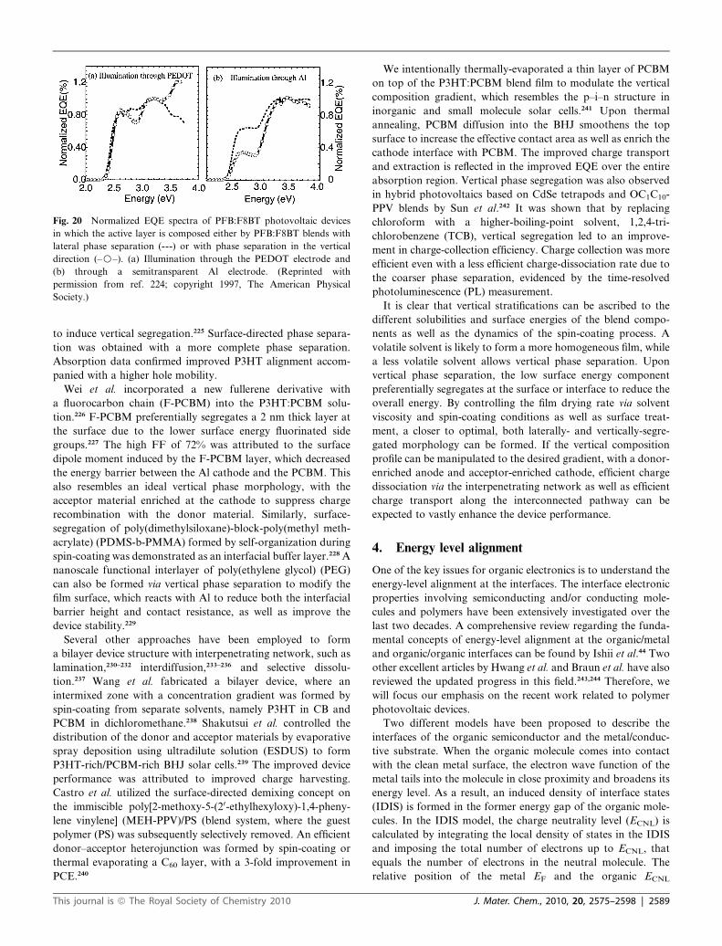
Fig. 20 Normalized EQE spectra of PFB:F8BT photovoltaic devices
in which the active layer is composed either by PFB:F8BT blends with
lateral phase separation (----) or with phase separation in the vertical
direction (–B–). (a) Illumination through the PEDOT electrode and
(b) through a semitransparent Al electrode. (Reprinted with
permission from ref. 224; copyright 1997, The American Physical
Society.)
to induce vertical segregation.225 Surface-directed phase separa-
tion was obtained with a more complete phase separation.
Absorption data confirmed improved P3HT alignment accom-
panied with a higher hole mobility.
Wei et al. incorporated a new fullerene derivative with
a fluorocarbon chain (F-PCBM) into the P3HT:PCBM solu-
tion.226 F-PCBM preferentially segregates a 2 nm thick layer at
the surface due to the lower surface energy fluorinated side
groups.227 The high FF of 72% was attributed to the surface
dipole moment induced by the F-PCBM layer, which decreased
the energy barrier between the Al cathode and the PCBM. This
also resembles an ideal vertical phase morphology, with the
acceptor material enriched at the cathode to suppress charge
recombination with the donor material. Similarly, surface-
segregation of poly(dimethylsiloxane)-block-poly(methyl meth-
acrylate) (PDMS-b-PMMA) formed by self-organization during
spin-coating was demonstrated as an interfacial buffer layer.228 A
nanoscale functional interlayer of poly(ethylene glycol) (PEG)
can also be formed via vertical phase separation to modify the
film surface, which reacts with Al to reduce both the interfacial
barrier height and contact resistance, as well as improve the
device stability.229
Several other approaches have been employed to form
a bilayer device structure with interpenetrating network, such as
lamination,230–232 interdiffusion,233–236 and selective dissolu-
tion.237 Wang et al. fabricated a bilayer device, where an
intermixed zone with a concentration gradient was formed by
spin-coating from separate solvents, namely P3HT in CB and
PCBM in dichloromethane.238 Shakutsui et al. controlled the
distribution of the donor and acceptor materials by evaporative
spray deposition using ultradilute solution (ESDUS) to form
P3HT-rich/PCBM-rich BHJ solar cells.239 The improved device
performance was attributed to improved charge harvesting.
Castro et al. utilized the surface-directed demixing concept on
the immiscible poly[2-methoxy-5-(20-ethylhexyloxy)-1,4-pheny-
lene vinylene] (MEH-PPV)/PS (blend system, where the guest
polymer (PS) was subsequently selectively removed. An efficient
donor–acceptor heterojunction was formed by spin-coating or
thermal evaporating a C60 layer, with a 3-fold improvement in
PCE.240
This journal is ª The Royal Society of Chemistry 2010
We intentionally thermally-evaporated a thin layer of PCBM
on top of the P3HT:PCBM blend film to modulate the vertical
composition gradient, which resembles the p–i–n structure in
inorganic and small molecule solar cells.241 Upon thermal
annealing, PCBM diffusion into the BHJ smoothens the top
surface to increase the effective contact area as well as enrich the
cathode interface with PCBM. The improved charge transport
and extraction is reflected in the improved EQE over the entire
absorption region. Vertical phase segregation was also observed
in hybrid photovoltaics based on CdSe tetrapods and OC1C10-
PPV blends by Sun et al.242 It was shown that by replacing
chloroform with a higher-boiling-point solvent, 1,2,4-tri-
chlorobenzene (TCB), vertical segregation led to an improve-
ment in charge-collection efficiency. Charge collection was more
efficient even with a less efficient charge-dissociation rate due to
the coarser phase separation, evidenced by the time-resolved
photoluminescence (PL) measurement.
It is clear that vertical stratifications can be ascribed to the
different solubilities and surface energies of the blend compo-
nents as well as the dynamics of the spin-coating process. A
volatile solvent is likely to form a more homogeneous film, while
a less volatile solvent allows vertical phase separation. Upon
vertical phase separation, the low surface energy component
preferentially segregates at the surface or interface to reduce the
overall energy. By controlling the film drying rate via solvent
viscosity and spin-coating conditions as well as surface treat-
ment, a closer to optimal, both laterally- and vertically-segre-
gated morphology can be formed. If the vertical composition
profile can be manipulated to the desired gradient, with a donor-
enriched anode and acceptor-enriched cathode, efficient charge
dissociation via the interpenetrating network as well as efficient
charge transport along the interconnected pathway can be
expected to vastly enhance the device performance.
4. Energy level alignment
One of the key issues for organic electronics is to understand the
energy-level alignment at the interfaces. The interface electronic
properties involving semiconducting and/or conducting mole-
cules and polymers have been extensively investigated over the
last two decades. A comprehensive review regarding the funda-
mental concepts of energy-level alignment at the organic/metal
and organic/organic interfaces can be found by Ishii et al.44 Two
other excellent articles by Hwang et al. and Braun et al. have also
reviewed the updated progress in this field.243,244 Therefore, we
will focus our emphasis on the recent work related to polymer
photovoltaic devices.
Two different models have been proposed to describe the
interfaces of the organic semiconductor and the metal/conduc-
tive substrate. When the organic molecule comes into contact
with the clean metal surface, the electron wave function of the
metal tails into the molecule in close proximity and broadens its
energy level. As a result, an induced density of interface states
(IDIS) is formed in the former energy gap of the organic mole-
cules. In the IDIS model, the charge neutrality level (ECNL) is
calculated by integrating the local density of states in the IDIS
and imposing the total number of electrons up to ECNL, that
equals the number of electrons in the neutral molecule. The
relative position of the metal EF and the organic ECNL
J. Mater. Chem., 2010, 20, 2575–2598 | 2589

Fig. 21 Schematic illustration of the evolution of the energy-level
alignment when a p-conjugated organic molecule or polymer is phys-
isorbed on a substrate surface when (a) FSUB > EICT+: Fermi-level
pinning to a positive integer charge-transfer state, (b) EICT� < FSUB <
EICT+: vacuum level alignment, and (c) FSUB < EICT�: Fermi-level
pinning to a negative integer charge-transfer state. The charge-transfer-
induced shift in vacuum level, D, is shown where applicable. (Reprinted
with permission from ref. 244; copyright 2009, Wiley VCH.)
Fig. 22 General FORG/SUB vs. FSUB dependence predicted by the ICT
model. (Reprinted with permission from ref. 244; copyright 2009, Wiley
VCH.)
determines the charge redistribution across the metal/organic
interface. The charge transfer forms an interfacial dipole that
narrows the energy difference between EF and ECNL. However,
the actual charge injection barrier also depends on the density of
states around ECNL and can be described by the following two
equations:
fBn ¼ S(fsub � EA) + (1 � S)ECNL (1)
S ¼ 1
1þ 4pe2Disd(2)
where fBn is the electron injection barrier, fsub is the work
function of the conductive substrate, EA is the electron affinity of
the organic semiconductor (energy difference between vacuum
and LUMO), Dis is the density of interface gap states, and d is the
effective metal–semiconductor distance.243
In contrast to organic small molecules deposited on the clean
metal surface in high vacuum systems, polymer films are coated
from solution to a substrate surface that is often contaminated
with hydrocarbons and/or native oxides. The contamination
layer physically and electronically decouples the polymer film
from the continuum of the metallic electronic states.245 Conse-
quently, vacuum level alignment (Schottky–Mott limit) holds at
the polymer/conductive substrate interface and the electron
injection barrier equals the difference between the substrate EF
and EA of the polymer (S ¼ 1).
In some cases, vacuum level shift is observed after polymer
coating on the conductive substrate, which can be explained
using the integer charge transfer (ICT) model. Although the
contamination layer decouples the polymer layer from the
substrate, charge transfer can still occur via tunneling as long as
the contamination layer is sufficiently thin. Since the organic
small molecules and conjugated polymers are soft materials,
adding or withdrawing charges induces substantial electronic
and geometric relaxation effects, leading to self-localized polar-
onic (single charge) or bipolaronic (double charge) states. These
states are located in the previously forbidden band gap of the
neutral molecule/polymer. The energy of the positive integer
charge transfer state, EICT+, is defined as the energy required to
take away one electron from the organic molecule or polymer,
resulting in a fully relaxed state. The energy of the negative
integer transfer state, EICT�, is defined as the energy gained by
adding one electron to the organic molecule or polymer to
produce a fully relaxed state. According to the ICT model, the
energy level alignment of an organic/conductive substrate system
with very weak interfacial interaction can be determined by the
work function of the substrate (FSUB) and the energy of the
charge transfer states of the organic material. If FSUB is larger
than EICT+ (Fig. 21a), electrons spontaneously flow from the
organic layer to the substrate, creating an interfacial dipole that
down-shifts the vacuum level. This process continues until the
interface dipole equals FSUB � EICT+ and the Fermi level is
pinned to the EICT+ state at the interface. Consequently, in this
condition the FORG/SUB remains invariant while the interface
dipole changes with FSUB. When FSUB lies between the EICT+
and the EICT� (Fig. 21b), no spontaneous charge transfer occurs
at the substrate–organic interface. Therefore, vacuum level
alignment holds and the work function of the substrate coated
with organic layer FORG/SUB equals FSUB. In the equilibrium
2590 | J. Mater. Chem., 2010, 20, 2575–2598
case where FSUB is smaller than EICT� (Fig. 21c), an interface
dipole equal to EICT� � FSUB is formed and the Fermi level is
pinned to the CT� state at the interface. The FORG/SUB in this
case is also independent of FSUB. Thus if the work function of the
conductive substrates spans a sufficiently large range, a depen-
dence between FSUB and the work function of the organic-on-
substrate interface FORG/SUB with sharp transitions between the
vacuum alignment (Schottky–Mott limit, EICT� < FSUB < EICT+
with FORG/SUB ¼ FSUB) and Fermi level pinning (FSUB < EICT�or FSUB > EICT+ with constant FORG/SUB) regimes are expected,
as shown in Fig. 22. However, in many experiments due to the
limitation of FSUB, only part of this region can be observed.
By using ultraviolet photoelectron spectroscopy (UPS),
Tengstedt et al. mapped out the energy level alignment of
4 conjugated polymers on various conductive substrates with the
This journal is ª The Royal Society of Chemistry 2010
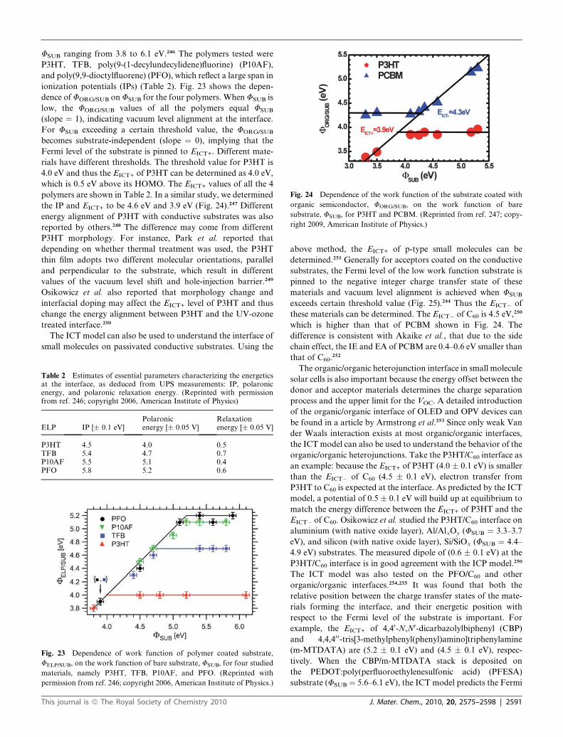
Fig. 24 Dependence of the work function of the substrate coated with
organic semiconductor, FORG/SUB, on the work function of bare
substrate, FSUB, for P3HT and PCBM. (Reprinted from ref. 247; copy-
right 2009, American Institute of Physics.)
FSUB ranging from 3.8 to 6.1 eV.246 The polymers tested were
P3HT, TFB, poly(9-(1-decylundecylidene)fluorine) (P10AF),
and poly(9,9-dioctylfluorene) (PFO), which reflect a large span in
ionization potentials (IPs) (Table 2). Fig. 23 shows the depen-
dence of FORG/SUB on FSUB for the four polymers. When FSUB is
low, the FORG/SUB values of all the polymers equal FSUB
(slope ¼ 1), indicating vacuum level alignment at the interface.
For FSUB exceeding a certain threshold value, the FORG/SUB
becomes substrate-independent (slope ¼ 0), implying that the
Fermi level of the substrate is pinned to EICT+. Different mate-
rials have different thresholds. The threshold value for P3HT is
4.0 eV and thus the EICT+ of P3HT can be determined as 4.0 eV,
which is 0.5 eV above its HOMO. The EICT+ values of all the 4
polymers are shown in Table 2. In a similar study, we determined
the IP and EICT+ to be 4.6 eV and 3.9 eV (Fig. 24).247 Different
energy alignment of P3HT with conductive substrates was also
reported by others.248 The difference may come from different
P3HT morphology. For instance, Park et al. reported that
depending on whether thermal treatment was used, the P3HT
thin film adopts two different molecular orientations, parallel
and perpendicular to the substrate, which result in different
values of the vacuum level shift and hole-injection barrier.249
Osikowicz et al. also reported that morphology change and
interfacial doping may affect the EICT+ level of P3HT and thus
change the energy alignment between P3HT and the UV-ozone
treated interface.250
The ICT model can also be used to understand the interface of
small molecules on passivated conductive substrates. Using the
Table 2 Estimates of essential parameters characterizing the energeticsat the interface, as deduced from UPS measurements: IP, polaronicenergy, and polaronic relaxation energy. (Reprinted with permissionfrom ref. 246; copyright 2006, American Institute of Physics)
ELP IP [� 0.1 eV]Polaronicenergy [� 0.05 V]
Relaxationenergy [� 0.05 V]
P3HT 4.5 4.0 0.5TFB 5.4 4.7 0.7P10AF 5.5 5.1 0.4PFO 5.8 5.2 0.6
Fig. 23 Dependence of work function of polymer coated substrate,
FELP/SUB, on the work function of bare substrate, FSUB, for four studied
materials, namely P3HT, TFB, P10AF, and PFO. (Reprinted with
permission from ref. 246; copyright 2006, American Institute of Physics.)
This journal is ª The Royal Society of Chemistry 2010
above method, the EICT+ of p-type small molecules can be
determined.251 Generally for acceptors coated on the conductive
substrates, the Fermi level of the low work function substrate is
pinned to the negative integer charge transfer state of these
materials and vacuum level alignment is achieved when FSUB
exceeds certain threshold value (Fig. 25).244 Thus the EICT� of
these materials can be determined. The EICT� of C60 is 4.5 eV,250
which is higher than that of PCBM shown in Fig. 24. The
difference is consistent with Akaike et al., that due to the side
chain effect, the IE and EA of PCBM are 0.4–0.6 eV smaller than
that of C60.252
The organic/organic heterojunction interface in small molecule
solar cells is also important because the energy offset between the
donor and acceptor materials determines the charge separation
process and the upper limit for the VOC. A detailed introduction
of the organic/organic interface of OLED and OPV devices can
be found in a article by Armstrong et al.253 Since only weak Van
der Waals interaction exists at most organic/organic interfaces,
the ICT model can also be used to understand the behavior of the
organic/organic heterojunctions. Take the P3HT/C60 interface as
an example: because the EICT+ of P3HT (4.0 � 0.1 eV) is smaller
than the EICT� of C60 (4.5 � 0.1 eV), electron transfer from
P3HT to C60 is expected at the interface. As predicted by the ICT
model, a potential of 0.5 � 0.1 eV will build up at equilibrium to
match the energy difference between the EICT+ of P3HT and the
EICT� of C60. Osikowicz et al. studied the P3HT/C60 interface on
aluminium (with native oxide layer), Al/AlxOy (FSUB ¼ 3.3–3.7
eV), and silicon (with native oxide layer), Si/SiOx (FSUB ¼ 4.4–
4.9 eV) substrates. The measured dipole of (0.6 � 0.1 eV) at the
P3HT/C60 interface is in good agreement with the ICP model.250
The ICT model was also tested on the PFO/C60 and other
organic/organic interfaces.254,255 It was found that both the
relative position between the charge transfer states of the mate-
rials forming the interface, and their energetic position with
respect to the Fermi level of the substrate is important. For
example, the EICT+ of 4,40-N,N0-dicarbazolylbiphenyl (CBP)
and 4,4,40 0-tris[3-methylphenyl(phenyl)amino]triphenylamine
(m-MTDATA) are (5.2 � 0.1 eV) and (4.5 � 0.1 eV), respec-
tively. When the CBP/m-MTDATA stack is deposited on
the PEDOT:poly(perfluoroethylenesulfonic acid) (PFESA)
substrate (FSUB ¼ 5.6–6.1 eV), the ICT model predicts the Fermi
J. Mater. Chem., 2010, 20, 2575–2598 | 2591

Fig. 25 Dependence of the work function of molecule-coated substrates,
FORG/SUB, on the work function of bare substrate, F SUB, for C60 (C),
TCNQ (-), and F4-TCNQ (:). (Reprinted with permission from ref.
244; copyright 2009, Wiley VCH.)
Fig. 26 UPS spectra and the corresponding diagrams of energy level
alignment of interfaces: (a) PEDOT-PFESA/CBP/m-MTDATA; (b)
Si/SiOx/CBP/m-MTDATA. (Reprinted with permission from ref. 255;
copyright 2009, American Institute of Physics.)
level alignment of the substrate with the EICT+ of CBP and
m-MTDATA, resulting a 0.7 eV dipole at the m-MTDATA on
CBP interface, which lowers the vacuum level to 4.6 eV
(Fig. 26a). In contrast, when a smaller work function silicon
Si/SiOxis used as the substructure, the ICT model predicts
vacuum level alignment at both the substrate/CBP and CBP/
m-MTDATA interfaces (Fig. 26b). The experimental results
correspond well with the ICT model predictions.255
From the ICT model, knowing the substrate work function
and the ICT states in organic materials constituting a multilay-
ered structure should enable the prediction of the energy level
alignment across the organic film stack. However, flat bilayer
interfaces do not exist in the blend systems and works revealing
2592 | J. Mater. Chem., 2010, 20, 2575–2598
the electronic structures in BHJs are scarce.247,256 We recently
used UPS to investigate the energy level alignment of the
P3HT:PCBM BHJ and showed that the ICT model can also be
employed to explain the results.
The EICT+ of P3HT and EICT� of PCBM were first determined
using the above method. (Fig. 24) Accordingly, the energy level
alignment between the P3HT (or PCBM) layer and the inert
substrates can be predicted using the ICT model. The work
function of PEDOT:PSS-coated ITO determined by UPS is 5.0
eV. Since this value is larger than the EICT+ of P3HT and lies
between the EICT+ and EICT� of PCBM, Fermi level pinning and
vacuum level alignment is expected at the PEDOT:PSS/P3HT
and the PEDOT:PSS/PCBM interface, respectively. As a result,
the FORG/SUB is anticipated to be 3.9 eV for PEDOT:PSS/P3HT
(Fig. 27a) and 5.0 eV for PEDOT:PSS/PCBM (Fig. 27b),
consistent with the results obtained from the secondary electron
cutoffs shown in Fig. 27d. Moreover, energy alignment of
PCBM/P3HT stack on PEDOT:PSS can also be predicted.
Because the EICT+ of P3HT is smaller than the EICT� of PCBM,
electrons will flow from P3HT to PCBM until the EICT+ state of
P3HT aligns with the EICT� state of PCBM at the interface. As
a result, an interface dipole of �0.4 eV forms and the vacuum
level of the P3HT layer is 4.6 eV above the Fermi level (FORG/SUB
¼ 4.6 eV) (Fig. 27). Fig. 27d shows the UPS spectra of different
P3HT:PCBM blends spin-coated on PEDOT:PSS. From the
HOMO structure (right) it can be found that the UPS signals of
the blend films are dominated by the P3HT component, which is
consistent with the vertical phase separation discussed previ-
ously. Moreover, the IPs calculated from the UPS spectra of the
blend films are around 4.6 eV and in agreement with ref. 246 and
250. The energy level alignment of the P3HT at the top surfaces
of the blend films can thus be acquired from the UPS spectra.
The UPS spectra of the blend films with low PCBM concentra-
tion (5:1, 3:1) are almost identical with pristine P3HT. Therefore,
the energy level alignment of P3HT at the top of the blend film is
the same as on PEDOT:PSS (or on top of the PEDOT:PSS/
PCBM/./P3HT stack, as predicted by the ICT model). As the
PCBM concentration increases, the UPS spectrum shifts to lower
binding energy, indicating a higher work function and a shal-
lower HOMO level. It should be noted that the energy levels
obtained from the UPS spectrum of the 1:5 weight ratio blend
film are almost the same as those of the P3HT layer shown in
Fig. 27c. In addition, the ICT model also predicts the same
results for the P3HT layer on top of the PEDOT:PSS/PCBM/
P3HT/./PCBM stack. These resemblances suggest that P3HT
covers most of the bottom surface (PEDOT:PSS/blends inter-
face) of the 5:1 blend film and PCBM dominates the equivalent
region of the 1:5 blend film. The PCBM/P3HT wt ratio at the
bottom surface of the 5:1 film is estimated to be about 0.25. This
value is much lower than the corresponding ratio of the 1:1 film,
where the ratio is estimated to be around 1.8. Campoy-Quiles
et al. estimated that the PCBM concentration at the PEDOT:PSS
side of the 1:1 blend film is about 65 vol%.34 Based on these data,
a full coverage of PCBM at the PEDOT:PSS side can be expected
in the 1:5 blend film.
The P3HT:PCBM blend films on Cs2CO3-covered ITO were
also investigated and confirmed the above finding. The work
function of Cs2CO3-coated ITO substrates can range from 3.05
to 3.8 eV, depending on different Cs2CO3 solution
This journal is ª The Royal Society of Chemistry 2010
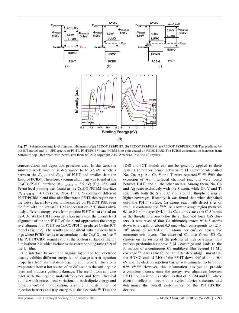
Fig. 27 Schematic energy level alignment diagrams of (a) PEDOT:PSS/P3HT, (b) PEDOT:PSS/PCBM, (c) PEDOT:PSS/PCBM/P3HT as predicted by
the ICT model and (d) UPS spectra of P3HT, P3HT:PCBM, and PCBM films spin-coated on PEDOT:PSS. The PCBM concentration increases from
bottom to top. (Reprinted with permission from ref. 247; copyright 2009, American Institute of Physics.)
concentrations and deposition processes used. In this case, the
substrate work function is determined to be 3.5 eV, which is
between the EICT+ and EICT� of P3HT and smaller than the
ECT� of PCBM. Therefore, vacuum alignment was found at the
Cs2CO3/P3HT interface (FORG/SUB ¼ 3.5 eV) (Fig. 28a) and
Fermi level pinning was found at the Cs2CO3/PCBM interface
(FORG/SUB ¼ 4.3 eV) (Fig. 28b). The UPS spectra of different
P3HT:PCBM blend films also illustrate a P3HT-rich region near
the top surface. However, unlike coated on PEDOT:PSS, even
the film with the lowest PCBM concentration (5:1) shows obvi-
ously different energy levels from pristine P3HT when coated on
Cs2CO3. As the P3HT concentration increases, the energy level
alignment of the top P3HT of the blend approaches the energy
level alignment of P3HT on Cs2CO3/P3HT predicted by the ICT
model (Fig. 28c). The results are consistent with previous find-
ings where PCBM tends to accumulate at the Cs2CO3 surface.28
The P3HT/PCBM weight ratio at the bottom surface of the 5:1
film is about 2.0, which is close to the corresponding ratio (2.2) of
the 1:1 film.
The interface between the organic layer and top electrode
usually exhibits different energetic and charge carrier injection
properties from its metal-on-organic counterpart. The atoms
evaporated from a hot source often diffuse into the soft organic
layer and induce significant damage. The metal atom can also
react with the organic molecule/polymer and form chemical
bonds, which causes local variations in both dipole energy and
molecular-orbital modification, creating a distribution of
injection barriers and trap energies at the electrode.244 Thus the
This journal is ª The Royal Society of Chemistry 2010
IDIS and ICT models can not be generally applied to these
systems. Interfaces formed between P3HT and vapor-deposited
Na, Cu, Ag, Au, Cr, V and Ti were reported.257–259 With the
exception of Au, interfacial chemical reactions were found
between P3HT and all the other metals. Among them, Na, Cu
and Ag react exclusively with the S atom, while Cr, V and Ti
react with both the S and C atoms of the thiophene ring at
higher coverages. Recently, it was found that when deposited
onto the P3HT surface, Ca atoms react with defect sites or
residual contamination.260,261 At a low coverage region (between
0.1 to 0.6 monolayer (ML)), the Ca atoms cleave the C–S bonds
in the thiophene group below the surface and form CaS clus-
ters. It was revealed that Ca ultimately reacts with S atoms
down to a depth of about 0.3 nm, which corresponds to 1.2 �1015 atoms of reacted sulfur atoms per cm2, or nearly five
monomer-unit layers. The adsorbed Ca also forms 3D Ca
clusters on the surface of the polymer at high coverages. This
process predominates above 2 ML coverage and leads to the
formation of a continuous Ca multilayer film beyond 11 ML
coverage.260 It was also found that after depositing 1 nm of Ca,
the HOMO and LUMO of the P3HT down-shifted about 0.4
eV and the electron injection barrier was estimated to be about
0.98 eV.261 However, this information has yet to provide
a complete picture, since the energy level alignment between
P3HT and Ca is not as critical as that of PCBM and Ca, where
electron collection occurs in a typical device structure, and
determines the overall performance of the P3HT:PCBM
devices.
J. Mater. Chem., 2010, 20, 2575–2598 | 2593

Fig. 28 Schematic energy level alignment diagrams of (a) Cs2CO3/P3HT, (b) Cs2CO3/PCBM, (c) Cs2CO3/PCBM/P3HT as predicted by the ICT model
and (d) UPS spectra of P3HT, P3HT:PCBM, and PCBM films spin-coated on Cs2CO3. The PCBM concentration increases from bottom to top.
(Reprinted with permission from ref. 247; copyright 2009, American Institute of Physics.)
Summary and outlook
The device performance of polymer solar cells depends on the
sequential processes of charge dissociation, transport, and
collection. The interfacial contact plays a central role in the
charge collection and vertical phase separation process. A
myriad of interfacial materials to engineer the anode and cathode
contacts are highlighted. The vertical phase morphology is of
fundamental importance to the charge-transport process, and
charge recombination can be reduced via an optimized vertical
composition gradient; that is, a donor-enriched anode and an
acceptor-enriched cathode. However, high performance photo-
voltaic cells cannot be obtained with an inferior interface
contact, and tremendous efforts are made to engineer the inter-
face at the nanoscale. A better understanding and control of the
interface properties of polymer solar cells shall allow us to derive
a general design rule to engineer future material systems for
polymer photovoltaic application.
With recent reports on significant advancement of donor
materials, record PCEs have been pushed forward from ca. 5% to
over 7% within the past few years, indicating promising potential
for further efficiency improvement.4,5 Though P3HT:PCBM
BHJs with different morphologies have been intensively studied
and well-understood with respect to electrode contact and
morphological characteristics, it is a unique system which only
provides limited information on the interface engineering for
future improvement. Molecular engineering usually aims to ach-
ieve polymers with tunable HOMO levels and band gaps that
2594 | J. Mater. Chem., 2010, 20, 2575–2598
ensure broad absorption and low potential loss. It requires
different building blocks to construct copolymers which generally
have lower crystallinity than P3HT. This lack of crystallinity leads
to alower mobility and carrier diffusion length. Consequently, the
film thicknesses and phase separation morphology are restricted
in BHJ photovoltaic cells based on these copolymers, while
commonly the amorphous films result in smaller carrier diffusion
length and uniform distribution of donor and acceptor. It is thus
more important to obtain highly selective and barrier-free charge
collection via utilizing proper functional interlayers. Meanwhile,
the surface effects on the polymer BHJ morphology should
provide further possibility to manipulate the film evolution
dynamics. Given efficient single BHJ photovoltaic cells with effi-
ciencies approaching 10%, it is also desirable to stack BHJs with
complementary absorption in tandem cells. The success in tandem
structures also lies in superior interface materials and sufficient
understanding of the interfacial contacts, which should help pave
the route towards a double-digit efficiency.
References
1 G. Li, V. Shrotriya, J. Huang, Y. Yao, T. Moriarty, K. Emery andY. Yang, Nat. Mater., 2005, 4, 864.
2 W. Ma, C. Yang, X. Gong, K. Lee and A. J. Heeger, Adv. Funct.Mater., 2005, 15, 1617.
3 J. Peet, J. Y. Kim, N. E. Coates, W. L. Ma, D. Moses, A. J. Heegerand G. C. Bazan, Nat. Mater., 2007, 6, 497.
4 S. H. Park, A. Roy, S. Beaupre, S. Cho, N. Coates, J. S. Moon,D. Moses, M. Leclerc, K. Lee and A. J. Heeger, Nat. Photonics,2009, 3, 297.
This journal is ª The Royal Society of Chemistry 2010

5 H.-Y. Chen, J. Hou, S. Zhang, Y. Liang, G. Yang, Y. Yang, L. Yu,Y. Wu and G. Li, Nat. Photonics, 2009, 3, 649.
6 I. D. Parker, J. Appl. Phys., 1994, 75, 1656.7 V. D. Mihailetchi, P. W. M. Blom, J. C. Hummelen and
M. T. Rispens, J. Appl. Phys., 2003, 94, 6849.8 J. Nelson, J. Kirkpatrick and P. Ravirajan, Phys. Rev. B: Condens.
Matter Mater. Phys., 2004, 69, 035337.9 B. P. Rand, D. P. Burk and S. R. Forrest, Phys. Rev. B: Condens.
Matter Mater. Phys., 2007, 75, 115327.10 T. Kirchartz, J. Mattheis and U. Rau, Phys. Rev. B: Condens. Matter
Mater. Phys., 2008, 78, 235320.11 J. J. Benson-Smith, L. Goris, K. Vandewal, K. Haenen, J. V. Manca,
D. Vanderzande, D. D. C. Bradley and J. Nelson, Adv. Funct.Mater., 2007, 17, 451.
12 K. Vandewal, K. Tvingstedt, A. Gadisa, O. Ingan€as andJ. V. Manca, Nat. Mater., 2009, 8, 904.
13 M. A. Loi, S. Toffanin, M. Muccini, M. Forster, U. Scherf andM. Scharber, Adv. Funct. Mater., 2007, 17, 2111.
14 M. Hallermann, S. Haneder and E. D. Como, Appl. Phys. Lett.,2008, 93, 053307.
15 D. Veldman, €O. Ipek, S. C. J. Meskers, J. Sweelssen, M. M. Koetse,S. C. Veenstra, J. M. Kroon, S. S. van Bavel, J. Loos andR. A. J. Janssen, J. Am. Chem. Soc., 2008, 130, 7721.
16 K. Vandewal, A. Gadisa, W. D. Oosterbaan, S. Bertho,F. Banishoeib, I. V. Severen, L. Lutsen, T. J. Cleij,D. Vanderzande and J. V. Manca, Adv. Funct. Mater., 2008, 18,2064.
17 Y. Hirose, A. Kahn, V. Aristov, P. Soukiassian, V. Bulovi andS. R. Forrest, Phys. Rev. B: Condens. Matter, 1996, 54, 13748.
18 P. Peumans, V. Bulovic and S. R. Forrest, Appl. Phys. Lett., 2000,76, 2650.
19 P. Peumans and S. R. Forrest, Appl. Phys. Lett., 2001, 79, 126.20 M. Vogel, S. Doka, Ch. Breyer, M. Ch. Lux-Steiner and
K. Fostiropoulos, Appl. Phys. Lett., 2006, 89, 163501.21 C. Waldauf, M. Morana, P. Denk, P. Schilinsky, K. Coakley,
S. A. Choulis and C. J. Brabec, Appl. Phys. Lett., 2006, 89, 233517.22 A. Hayakawa, O. Yoshikawa, T. Fujieda, K. Uehara and
S. Yoshikawa, Appl. Phys. Lett., 2007, 90, 163517.23 M. D. Irwin, D. B. Buchholz, A. W. Hains, R. P. H. Chang and
T. J. Marks, Proc. Natl. Acad. Sci. U. S. A., 2008, 105, 2783.24 L. S. Hung and C. H. Chen, Mater. Sci. Eng., R, 2002, 39, 143.25 K. Walzer, B. Maennig, M. Pfeiffer and K. Leo, Chem. Rev., 2007,
107, 1233.26 G. Li, C.-W. Chu, V. Shrotriya, J. Huang and Y. Yang, Appl. Phys.
Lett., 2006, 88, 253503.27 S. K. Hau, H.-L. Yip, N. S. Baek, J. Zou, K. O’Malley and A. K.-
Y. Jen, Appl. Phys. Lett., 2008, 92, 253301.28 Z. Xu, L.-M. Chen, G. W. Yang, C.-H. Huang, J. H. Hou, Y. Wu,
G. Li, C.-S. Hsu and Y. Yang, Adv. Funct. Mater., 2009, 19, 1227.29 L.-M. Chen, Z. Hong, G. Li and Y. Yang, Adv. Mater., 2009, 21,
1434.30 R. A. L. Jones, L. J. Norton, E. J. Kramer, F. S. Bates and
P. Wiltzius, Phys. Rev. Lett., 1991, 66, 1326.31 G. Krausch, C. A. Dai, E. J. Kramer, J. Marko and F. S. Bates,
Macromolecules, 1993, 26, 5566.32 S. Walheim, M. B€oltau, J. Mlynek, G. Krausch and U. Steiner,
Macromolecules, 1997, 30, 4995.33 S. Khodabakhsh, B. M. Sanderson, J. Nelson and T. S. Jones, Adv.
Funct. Mater., 2006, 16, 95.34 M. Campoy-Quiles, T. Ferenczi, T. Agostinelli, P. G. Etchegoin,
Y. Kim, T. D. Anthopoulos, P. N. Stavrinou, D. D. C. Bradleyand J. Nelson, Nat. Mater., 2008, 7, 158.
35 S. T. Lee, Z. Q. Gao and L. S. Hung, Appl. Phys. Lett., 1999, 75,1404.
36 K. Suemori, M. Yokoyama and M. Hiramoto, J. Appl. Phys., 2006,99, 036109.
37 C. Uhrich, R. Schueppel, A. Petrich, M. Pfeiffer, K. Leo, E. Brier,P. Kilickiran and P. Baeuerle, Adv. Funct. Mater., 2007, 17, 2991.
38 A. Kumar, S. Sista and Y. Yang, J. Appl. Phys., 2009, 105, 094512.39 J. Y. Kim, S. H. Kim, H. H. Lee, K. H. Lee, W. L. Ma, X. Gong and
A. J. Heeger, Adv. Mater., 2006, 18, 572.40 A. Roy, S. H. Park, S. Cowan, M. H. Tong, S. Cho, K. Lee and
A. J. Heeger, Appl. Phys. Lett., 2009, 95, 013302.41 J. Gilot, I. Barbu, M. M. Wienk and R. A. J. Janssen, Appl. Phys.
Lett., 2007, 91, 113520.
This journal is ª The Royal Society of Chemistry 2010
42 B. V. Andersson, D. M. Huang, A. J. Moul�e and O. Ingan€as, Appl.Phys. Lett., 2009, 94, 043302.
43 N. Uyeda, T. Kobayashi, K. Ishizuka and Y. Fujiyoshi, Nature,1980, 285, 95.
44 H. Ishii, K. Sugiyama, E. Ito and K. Seki, Adv. Mater., 1999, 11, 605.45 Y. Hirose, A. Kahn, V. Arisotov and P. Soukiassian, Appl. Phys.
Lett., 1996, 68, 217.46 H. Oji, E. Ito, M. Furuta, K. Kajikawa, H. Ishii, Y. Ouchi and
K. Seki, J. Electron Spectrosc. Relat. Phenom., 1999, 101–103, 517.47 S. K. Hau, H.-L. Yip, K. Leong and A. K.-Y. Jen, Org. Electron.,
2009, 10, 719.48 J.-Y. Lee, S. T. Connor, Y. Cui and P. Peumans, Nano Lett., 2008, 8,
689.49 M. L€ogdlund and J. L. Br�edas, J. Chem. Phys., 1994, 101, 4357.50 H. Antoniadis, B. R. Hsieh, M. A. Abkowitz, S. A. Jenekhe and
M. Stolka, Synth. Met., 1994, 62, 265.51 G. Yu, C. Zhang and A. J. Heeger, Appl. Phys. Lett., 1994, 64, 1540.52 G. Yu, K. Pakbaz and A. J. Heeger, Appl. Phys. Lett., 1994, 64, 3422.53 C. J. Brabec, A. Cravino, D. Meissner, N. S. Sariciftci, T. Fromherz,
M. T. Rispents, L. Sanchez and J. C. Hummelen, Adv. Funct. Mater.,2001, 11, 374.
54 D. Gupta, M. Bag and K. S. Narayan, Appl. Phys. Lett., 2008, 92,093301.
55 J. M. Bharathan and Y. Yang, J. Appl. Phys., 1998, 84, 3207.56 S. Cros, M. Firon, S. Lenfant, P. Trouslard and L. Beck, Nucl.
Instrum. Methods Phys. Res., Sect. B, 2006, 251, 257.57 M. O. Reese, M. S. White, G. Rumbles, D. S. Ginley and
S. E. Shaheen, Appl. Phys. Lett., 2008, 92, 053307.58 L. S. Hung, C. W. Tang and M. G. Mason, Appl. Phys. Lett., 1997,
70, 152.59 S. E. Shaheen, G. E. Jabbour, M. M. Morrell, Y. Kawabe,
B. Kippelen, N. Peyghambarian, M.-F. Nabor, R. Schlaf,E. A. Mash and N. R. Armstrong, J. Appl. Phys., 1998, 84, 2324.
60 L. S. Hung, R. Q. Zhang, P. He and M. G. Mason, J. Phys. D: Appl.Phys., 2002, 35, 103.
61 G. E. Jabbour, B. Kippelen, N. R. Armstrong andN. Peyghambarian, Appl. Phys. Lett., 1998, 73, 1185.
62 T. Hasegawa, S. Miura, T. Moriyama, T. Kimura, I. Takaya,Y. Osato and H. Mizutani, in SID Int. Symp. Digest Technol.Papers, 2004, p. 154.
63 J. Huang, G. Li, E. Wu, Q. Xu and Y. Yang, Adv. Mater., 2006, 18,114.
64 J. Huang, T. Watanabe, K. Ueno and Y. Yang, Adv. Mater., 2007,19, 739.
65 Y. J. Yi, S. J. Kang, K. Cho, J. M. Koo, K. Han, K. J. Park,M. K. Noh, C. N. Whang and K. H. Jeong, Appl. Phys. Lett.,2005, 86, 213502.
66 Y. Kim, J.-G. Lee and S. Kim, Adv. Mater., 1999, 11, 1463.67 X. T. Tao, H. Suzuki, T. Wada, S. Miyata and H. Sasabe, J. Am.
Chem. Soc., 1999, 121, 9447.68 C. Ganzorig, K. Suga and M. Fujihira, Mater. Sci. Eng., B, 2001, 85,
140.69 J. Lee, Y. Park, S. K. Lee, E.-J. Cho, D. Y. Kim, H. Y. Chu, H. Lee,
L.-M. Do and T. Zyung, Appl. Phys. Lett., 2002, 80, 3123.70 J. Lee, Y. Park, D. Y. Kim, H. Y. Chu, H. Lee and L.-M. Do, Appl.
Phys. Lett., 2003, 82, 173.71 S. E. Shaheen, C. J. Brabec, N. S. Sariciftci, F. Padinger,
T. Fromherz and J. C. Hummelen, Appl. Phys. Lett., 2001, 78, 841.72 C. J. Brabec, S. E. Shaheen, C. Winder, N. S. Sacriciftci and P. Denk,
Appl. Phys. Lett., 2002, 80, 1288.73 W. J. H. van Gennip, J. K. J. van Duren, P. C. Thune,
R. A. J. Janssen and J. W. Niemantsverdriet, J. Chem. Phys.,2002, 117, 5031.
74 B. N. Limketkai and M. A. Baldo, Phys. Rev. B: Condens. MatterMater. Phys., 2005, 71, 085207.
75 S. K. M. J€onsson, E. Carlegrim, F. Zhang, W. R. Salaneck andM. Fahlman, Jpn. J. Appl. Phys., 2005, 44, 3695.
76 C. H. Lee, Synth. Met., 1997, 91, 125.77 Y. S. Lee, J.-H. Park, Y.-H. Kwak, Y.-J. Kim and J. S. Choi, Mol.
Cryst. Liq. Cryst., 2003, 405, 89.78 J. Lee, Y. Park, D. Y. Kim, H. Y. Chu, H. Lee and L. M. Do, Appl.
Phys. Lett., 2003, 82, 173.79 S. Okada, K. Okinaka, H. Iwawaki, M. Furugori, M. Hashimoto,
T. Mukaide, J. Kamatani, S. Igawa, A. Tsuboyama, T. Takiguchiand K. Ueno, Dalton Trans., 2005, 1583.
J. Mater. Chem., 2010, 20, 2575–2598 | 2595
80 E. Ahlswede, J. Hanisch and M. Powalla, Appl. Phys. Lett., 2007, 90,163504.
81 J. Huang, W. J. Hou, J. H. Li, G. Li and Y. Yang, Appl. Phys. Lett.,2006, 89, 133509.
82 J. Huang, Z. Xu and Y. Yang, Adv. Funct. Mater., 2007, 17, 1966.83 T. R. Briere and A. H. Sommer, J. Appl. Phys., 1977, 48, 3547.84 C.-I. Wu, C.-T. Lin, Y.-H. Chen, M.-H. Chen, Y.-J. Lu and C.-
C. Wu, Appl. Phys. Lett., 2006, 88, 152104.85 M.-H. Chen and C.-I. Wu, J. Appl. Phys., 2008, 104, 113713.86 A. H. Sommer, J. Appl. Phys., 1980, 51, 1254.87 H.-H. Liao, L.-M. Chen, Z. Xu, G. Li and Y. Yang, Appl. Phys.
Lett., 2008, 92, 173303.88 F.-C. Chen, J.-L. Wu, S. S. Yang, K.-H. Hsieh and W.-C. Chen,
J. Appl. Phys., 2008, 103, 103721.89 F.-C. Chen, J.-L. Wu, K.-H. Hsieh, W.-C. Chen and S.-W. Lee, Org.
Electron., 2008, 9, 1132.90 A. Fujishima and K. Honda, Nature, 1972, 238, 37.91 B. O’Regan and M. Gr€atzel, Nature, 1991, 353, 737.92 A. Fujishima, T. N. Rao and D. A. Tryk, J. Photochem. Photobiol.,
C, 2000, 1, 1.93 A. L. Linsebigler, G. Lu and J. J. T. Yates, Chem. Rev., 1995, 95,
735.94 K. H. Lee, J. Y. Kim, S. H. Park, S. H. Kim, S. N. Cho and
A. J. Heeger, Adv. Mater., 2007, 19, 2445.95 J. K. Lee, N. E. Coates, S. Cho, N. S. Cho, D. Moses, G. C. Bazan,
K. Lee and A. J. Heeger, Appl. Phys. Lett., 2008, 92, 243308.96 J. C. Yu, J. Yu, W. Ho, Z. Jiang and L. Zhang, Chem. Mater., 2002,
14, 3808.97 C. Burda, Y. Lou, X. Chen, A. C. S. Samia, J. Stout and J. L. Gole,
Nano Lett., 2003, 3, 1049.98 N. Sekine, C.-H. Chou, W. L. Kwan and Y. Yang, Org. Electron.,
2009, 10, 1473.99 M.-H. Park, J.-H. Li, A. Kumar, G. Li and Y. Yang, Adv. Funct.
Mater., 2009, 19, 1241.100 J. Y. Kim, K. H. Lee, N. E. Coates, D. Moses, T.-Q. Nguyen,
M. Dante and A. J. Heeger, Science, 2007, 317, 222.101 J. H. Hou, H.-Y. Chen, S. Zhang, G. Li and Y. Yang, J. Am. Chem.
Soc., 2008, 130, 16144.102 S. Sista, M.-H. Park, Z. R. Hong, Y. Wu, J. H. Hou, W. L. Kwan,
G. Li and Y. Yang, Adv. Mater., 2010, 22, 380, DOI: 10.1002/adma.200901624.
103 T. Kuwabara, H. Sugiyama, T. Yamaguchi and K. Takahashi, ThinSolid Films, 2009, 517, 3766.
104 A. L. Roest, J. J. Kelly, D. Vanmaekelbergh and E. A. Meulenkamp,Phys. Rev. Lett., 2002, 89, 036801.
105 J. Gilot, M. M. Wienk and R. A. J. Janssen, Appl. Phys. Lett., 2007,90, 143512.
106 W. J. E. Beek, M. M. Wienk, M. Kemerink, X. Yang andR. A. J. Janssen, J. Phys. Chem. B, 2005, 109, 9505.
107 F. Verbakel, S. C. J. Meskers and R. A. J. Janssen, Appl.Phys. Lett.,2006, 89, 102103.
108 B. Maennig, J. Drechsel, D. Gebeyehu, P. Simon, F. Kozlowski,A. Werner, F. Li, S. Grundmann, S. Sonntag, M. Koch, K. Leo,M. Pfeiffer, H. Hoppe, D. Meissner, N. S. Sariciftci, I. Riedel,V. Dyakonov and J. Parisi, Appl. Phys. A: Mater. Sci. Process.,2004, 79, 1.
109 J. S. Kim, J. H. Park, J. H. Lee, J. Jo, D.-Y. Kim and K. Cho, Appl.Phys. Lett., 2007, 91, 112111.
110 S. Khodabakhsh, D. Poplavskyy, S. Heutz, J. Nelson,D. D. C. Bradley, H. Murata and T. S. Jones, Adv. Funct. Mater.,2004, 14, 1205.
111 S. K. Hau, H.-L. Yip, O. Acton, N. S. Baek, H. Ma and A. K.-Y. Jen, J. Mater. Chem., 2008, 18, 5113.
112 G. K. Mor, K. Shankar, M. Paulose, O. K. Varghese andC. A. Grimes, Appl. Phys. Lett., 2007, 91, 152111.
113 T. C. Monson, M. T. Lloyd, D. C. Olson, Y.-J. Lee and J. W. P. Hsu,Adv. Mater., 2008, 20, 4755.
114 J. Veres, S. Ogier, G. Lloyd and D. d. Leeuw, Chem. Mater., 2004,16, 4543.
115 I.-W. Hwang, C. Soci, D. Moses, Z. Zhu, D. Waller, R. Gaudiana,C. J. Brabec and A. J. Heeger, Adv. Mater., 2007, 19, 2307.
116 H.-L. Yip, S. K. Hau, N. S. Baek and A. K.-Y. Jen, Appl. Phys. Lett.,2008, 92, 193313.
117 H.-L. Yip, S. K. Hau, N. S. Baek, H. Ma and A. K.-Y. Jen, Adv.Mater., 2008, 20, 2376.
2596 | J. Mater. Chem., 2010, 20, 2575–2598
118 F. Zhang, M. Ceder and O. Ingan€as, Adv. Mater., 2007, 19, 1835.119 X. H. Chen, J. X. Yang, J. Lu, K. K. Manga, K. P. Loh and
F. R. Zhu, Appl. Phys. Lett., 2009, 95, 133305.120 J. Luo, H. B. Wu, C. He, A. Y. Li, W. Yang and Y. Cao, Appl. Phys.
Lett., 2009, 95, 043301.121 Y. Zhao, Z. Y. Xie, C. J. Qin, Yao Qu, Y. H. Geng and L. X. Wang,
Sol. Energy Mater. Sol. Cells, 2009, 93, 604.122 S.-I. Na, S.-H. Oh, S.-S. Kim and D.-Y. Kim, Org. Electron., 2009,
10, 496.123 Y. Cao, G. Yu, C. Zhang, R. Menon and A. J. Heeger, Synth. Met.,
1997, 87, 171.124 Y.-F. Lim, S. Lee, D. J. Herman, M. T. Lloyd, J. E. Anthony and
G. G. Malliaras, Appl. Phys. Lett., 2008, 93, 193301.125 M. P. de Jong, L. J. van IJzendoorn and M. J. A. d. Voigt, Appl.
Phys. Lett., 2000, 77, 2255.126 Y. H. Kim, S.-H. Lee, J. Noh and S.-H. Han, Thin Solid Films, 2006,
510, 305.127 K. W. Wong, H. L. Yip, Y. Luo, K. Y. Wong, W. M. Lau,
K. H. Low, H. F. Chow, Z. Q. Gao, W. L. Yeung andC. C. Chang, Appl. Phys. Lett., 2002, 80, 2788.
128 H. Yan, P. Lee, N. R. Armstrong, A. Graham, G. A. Evmenenko,P. Dutta and T. J. Marks, J. Am. Chem. Soc., 2005, 127, 3172.
129 V. Shrotriya, G. Li, Y. Yao, C. Chu and Y. Yang, Appl. Phys. Lett.,2006, 88, 073508.
130 D. Y. Kim, J. Subbiah, G. Sarasqueta, F. So, H. J. Ding, Irfan andY. L. Gao, Appl. Phys. Lett., 2009, 95, 093304.
131 D. Y. Kim, G. Sarasqueta and F. So, Sol. Energy Mater. Sol. Cells,2009, 93, 1452.
132 D. W. Zhao, W. S. X, C. Y. Jiang, A. K. K. Kyaw, G. Q. Lo andD. L. Kwong, Appl. Phys. Lett., 2008, 93, 083305.
133 N. Li, B. E. Lassiter, R. R. Lunt, G. Wei and S. R. Forrest, Appl.Phys. Lett., 2009, 94, 023307.
134 S. Han, W. S. Shin, M. Seo, D. Gupta, S.-J. Moon and S. Yoo, Org.Electron., 2009, 10, 791.
135 M. Y. Chan, C. S. Lee, S. L. Lai, M. K. Fung, F. L. Wong,H. Y. Sun, K. M. Lau and S. T. Lee, J. Appl. Phys., 2006, 100,094506.
136 M. Kr€oger, S. Hamwi, J. Meyer, T. Riedl, W. Kowalsky andA. Kahn, Appl. Phys. Lett., 2009, 95, 123301.
137 J. Cui, Q. Huang, J. C. G. Veinot, H. Yan, Q. Wang,G. R. Hutchison, A. G. Richter, G. Evmenenko, P. Dutta andT. J. Marks, Langmuir, 2002, 18, 9958.
138 A. W. Hains and T. J. Marks, Appl. Phys. Lett., 2008, 92, 023504.139 B. Kang, L. W. Tan and S. R. P. Silva, Appl. Phys. Lett., 2008, 93,
133302.140 C.-Y. Li, T.-C. Wen and T.-F. Guo, J. Mater. Chem., 2008, 18,
4478.141 M. S. White, D. C. Olson, S. E. Shaheen, N. Kopidakis and
D. S. Ginley, Appl. Phys. Lett., 2006, 89, 143517.142 M. Andersen, J. E. Carle, N. Cruys-Bagger, M. R. Lilliedal,
M. A. Hammond, B. Winther-Jensen and F. C. Krebs, Sol. EnergyMater. Sol. Cells, 2007, 91, 539.
143 Y. K. Kim, S. A. Choulis, J. Nelson, D. D. C. Bradley, S. Cook andJ. R. Durrant, Appl. Phys. Lett., 2005, 86, 063502.
144 R. Steim, S. A. Choulis, P. Schilinsky and C. J. Brabec, Appl. Phys.Lett., 2008, 92, 093303.
145 T. Ameri, G. Dennler, C. Waldauf, P. Denk, K. Forberich,M. C. Scharber, C. J. Brabec and K. Hingerl, J. Appl. Phys., 2008,103, 084506.
146 A. K. K. Kyaw, X. W. Sun, C. Y. Jiang, G. Q. Lo, D. W. Zhao andD. L. Kwong, Appl. Phys. Lett., 2008, 93, 221107.
147 S. O’Brien, L. H. K. Koh and G. M. Crean, Thin Solid Films, 2008,516, 1391.
148 D. W. Zhao, P. Liu, X. W. Sun, S. T. Tan, L. Ke and A. K. K. Kyaw,Appl. Phys. Lett., 2009, 95, 153304.
149 J. B. Kim, C. S. Kim, Y. S. Kim and Y.-L. Loo, Appl. Phys. Lett.,2009, 95, 183301.
150 K. Takanezawa, K. Tajima and K. Hashimoto, Appl. Phys. Lett.,2008, 93, 063308.
151 J. Ouyang and Y. Yang, Adv. Mater., 2006, 18, 2141.152 J. Huang, G. Li and Y. Yang, Adv. Mater., 2008, 20, 415.153 V. Shrotriya, E. H.-E. Wu, G. Li, Y. Yao and Y. Yang, Appl. Phys.
Lett., 2006, 88, 064104.154 T. Oyamada, Y. Sugawara, Y. Terao, H. Sasabe and C. Adachi, Jpn.
J. Appl. Phys., 2007, 46, 1734.
This journal is ª The Royal Society of Chemistry 2010

155 R. F. Bailey-Salzman, B. P. Rand and S. R. Forrest, Appl. Phys.Lett., 2006, 88, 233502.
156 G.-M. Ng, E. L. Kietzke, T. Kietzke, L.-W. Tan, P.-K. Liew andF. Zhu, Appl. Phys. Lett., 2007, 90, 103505.
157 J. Hanisch, E. Ahlswede and M. Powalla, Eur. Phys. J.: Appl. Phys.,2007, 37, 261.
158 F.-C. Chen, J.-L. Wu, C.-L. Lee, W.-C. Huang, H.-M. P. Chen andW.-C. Chen, IEEE Electron Device Lett., 2009, 30, 727.
159 H. Schmidt, H. Fl€ugge, T. Winkler, T. B€ulow, T. Riedl andW. Kowalsky, Appl. Phys. Lett., 2009, 94, 243302.
160 C. Tao, S. P. Ruan, G. H. Xie, X. Z. Kong, L. Shen, F. X. Meng,C. X. Liu, X. D. Zhang, W. Dong and W. Y. Chen, 2009, 94, p. 043311.
161 K. M. Coakley and M. D. McGehee, Chem. Mater., 2004, 16, 4533.162 J. S. Huang, C.-Y. Chou, M.-Y. Liu, K.-H. Tsai, W.-H. Lin and C.-
F. Lin, Org. Electron., 2009, 10, 1060.163 W.-H. Baek, I. Seo, T.-S. Yoon, H. H. Lee, C. M. Yun and Y.-
S. Kim, Sol. Energy Mater. Sol. Cells, 2009, 93, 1587.164 B. Y. Yu, A. Tsai, S. P. Tsai, K. T. Wong, Y. Yang, C.-W. Chu and
J. J. Shyue, Nanotechnology, 2008, 19, 255202.165 K. M. Coakley, B. S. Srinivasan, J. M. Ziebarth, C. Goh, Y. Liu and
M. D. McGehee, Adv. Funct. Mater., 2005, 15, 1927.166 G. K. Mor, K. Shankar, M. Paulose, O. K. Varghese and
C. A. Grimes, Appl. Phys. Lett., 2007, 91, 152111.167 M. Geoghegan, Prog. Polym. Sci., 2003, 28, 261.168 A. Budkowski, A. Bernasik, P. Cyganik, J. Raczkowska, B. Penc,
B. Bergues, K. Kowalski, J. Rysz and J. Janik, Macromolecules,2003, 36, 4060.
169 J. Genzer and E. J. Kramer, Phys. Rev. Lett., 1997, 78, 4946.170 U. Steiner, J. Klein, E. Eiser, A. Budkowski and L. J. Fetters,
Science, 1992, 258, 1126.171 G. Krausch, Mater. Sci. Eng., R, 1995, 14, v.172 F. Bruder and R. Brenn, Phys. Rev. Lett., 1992, 69, 624.173 C. Ton-That, A. G. Shard, D. O. H. Teare and R. H. Bradley,
Polymer, 2001, 42, 1121.174 M. B€oltau, S. Walheim, J. Mlynek, G. Krausch and U. Steiner,
Nature, 1998, 391, 877.175 S. Y. Heriot and R. A. L. Jones, Nat. Mater., 2005, 4, 782.176 J. Raczkowska, A. Bernasik, A. Budkowski, K. Sajewicz, B. Penc,
J. Lekki, M. Lekka, J. Rysz, K. Kowalski and P. Czuba,Macromolecules, 2004, 37, 7308.
177 A. C. Arias, N. Corcoran, M. Banach, R. H. Friend,J. D. MacKenzie and W. T. S. Huck, Appl. Phys. Lett., 2002, 80,1695.
178 J. Chappell, D. G. Lidzey, P. C. Jukes, A. M. Higgins,R. L. Thompson, S. O’Connor, I. Grizzi, R. Fletcher, J. O’Brien,M. Geoghegan and R. A. L. Jones, Nat. Mater., 2003, 2, 616.
179 J.-S. Kim, P. K. H. Ho, C. E. Murphy and R. H. Friend,Macromolecules, 2004, 37, 2861.
180 A. M. Higgins, S. J. Martin, R. L. Thompson, J. Chappell, M. Voigt,D. G. Lidzey, R. A. L. Jones and M. Geoghegan, J. Phys.: Condens.Matter, 2005, 17, 1319.
181 J. J. M. Halls, A. C. Arias, J. D. MacKenzie, W. S. Wu,M. Inbasekaran, E. P. Woo and R. H. Friend, Adv. Mater., 2000,12, 498.
182 A. C. Arias, J. D. MacKenzie, R. Stevenson, J. J. M. Halls,M. Inbasekaran, E. P. Woo, D. Richards and R. H. Friend,Macromolecules, 2001, 34, 6005.
183 S. Goffri, C. M€uller, N. Stingelin-Stutzmann, D. W. Breiby,C. P. Radano, J. W. Andreasen, R. Thompson, R. A. J. Janssen,M. M. Nielsen, P. Smith and H. Sirringhaus, Nat. Mater., 2006, 5,950.
184 A. C. Arias, J. D. MacKenzie, R. Stevenson, J. J. M. Halls,M. Inbasekaran, E. P. Woo, D. Richards and R. H. Friend,Macromolecules, 2001, 34, 6005.
185 L.-L. Chua, P. K. H. Ho, H. Sirringhaus and R. H. Friend, Appl.Phys. Lett., 2004, 84, 3400.
186 A. C. Arias, F. Endicott and R. A. Street, Adv.Mater., 2006, 18,2900.
187 L. Z. Qiu, J. A. Lim, X. H. Wang, W. H. Lee, M. K. Hwang andK. Cho, Adv. Mater., 2008, 20, 1141.
188 G. Greczynski, T. Kugler and W. R. Salaneck, Thin Solid Films,1999, 354, 129.
189 A. M. Higgins, S. J. Martin, P. C. Jukes, M. Geoghegan,R. A. L. Jones, S. Langridge, R. Cubitt, S. Kirchmeyer,A. Wehrum and I. Grizzi, J. Mater. Chem., 2003, 13, 2814.
This journal is ª The Royal Society of Chemistry 2010
190 H. J. Snaith, H. Kenrick, M. Chiesa and R. H. Friend, Polymer,2005, 46, 2573.
191 L. H. Slooff, S. C. Veenstra, J. M. Kroon, D. J. D. Moet,J. Sweelssen and M. M. Koetse, Appl. Phys. Lett., 2007, 90,143506.
192 O. Ingan€as, F. L. Zhang and M. Andersson, Acc. Chem. Res., 2009,42, 1731.
193 A. Bernasik, J. Rysz, A. Budkowski, K. Kowalski, J. Camra andJ. Jedliski, Macromol. Rapid Commun., 2001, 22, 829.
194 C. M. Bj€orstr€om, A. Bernasik, J. Rysz, A. Budkowski, S. Nilsson,M. Svensson, M. R. Andersson, K. O. Magnusson and E. Moons,J. Phys.: Condens. Matter, 2005, 17, L529.
195 C. M. Bj€orstr€om Svanstr€om, J. Rysz, A. Bernasik, A. Budkowski,F. L. Zhang, O. Ingan€as, M. R. Andersson, K. O. Magnusson,J. J. Benson-Smith, J. Nelson and E. Moons, Adv. Mater., 2009,21, 4398.
196 G. Dennler, H.-J. Prall, R. Koeppe, M. Egginger, R. Autengruberand N. S. Sariciftci, Appl. Phys. Lett., 2006, 89, 073502.
197 H.-J. Prall, R. Koeppe, R. Autengruber, M. Egginger, G. Dennlerand N. S. Sariciftci, in Proc. of the Soc. of Photo-OpticalInstrumentation Engineers, ed. A. Gombert, SPIE, Bellingham,WA, 2006, p. F1970.
198 S. Nilsson, A. Bernasik, A. Budkowski and E. Moons,Macromolecules, 2007, 40, 8291.
199 L. M. Andersson and O. Ingan€as, Appl. Phys. Lett., 2006, 88,082103.
200 V. D. Mihailetchi, L. J. A. Koster, P. W. M. Blom, C. Melzer, B. deBoer, J. K. J. van Duren and R. A. J. Janssen, Adv. Funct. Mater.,2005, 15, 795.
201 L. M. Andersson, F. Zhang and O. Ingan€as, Appl. Phys. Lett., 2007,91, 071108.
202 H. Hoppe, T. Glatzel, M. Niggemann, A. Hinsch, M. C. Lux-Steinerand N. S. Sariciftci, Nano Lett., 2005, 5, 269.
203 C. M. Bj€orstr€om, S. Nilsson, A. Bernasik, A. Budkowski,M. Andersson, K. O. Magnusson and E. Moons, Appl. Surf. Sci.,2007, 253, 3906.
204 A. J. Moul�e and K. Meerholz, Adv. Mater., 2008, 20, 240.205 J. K. Lee, W. L. Ma, C. J. Brabec, J. Yuen, J. S. Moon, J. Y. Kim,
K. Lee, G. C. Bazan and A. J. Heeger, J. Am. Chem. Soc., 2008, 130,3619.
206 Y. Yao, J. H. Hou, Z. Xu, G. Li and Y. Yang, Adv. Funct. Mater.,2008, 18, 1783.
207 C. S. Kim, L. L. Tinker, B. F. Disalle, E. D. Gomez, S. Lee,S. Bernhard and Y.-L. Loo, Adv. Mater., 2009, 21, 3110.
208 K. Ohno and Y. Kawazoe, Scr. Mater., 2001, 44, 1579.209 R. J. Kline, D. M. DeLongchamp, D. A. Fischer, E. K. Lin,
M. Heeney, I. McCulloch and M. F. Toney, Appl. Phys. Lett.,2007, 90, 062117.
210 D. S. Germack, C. K. Chan, B. H. Hamadani, L. J. Richter,D. A. Fischer, D. J. Gundlach and D. M. DeLongchamp, Appl.Phys. Lett., 2009, 94, 233303.
211 M. P. Felicissimo, D. Jarzab, M. Gorgoi, M. Forster, U. Scherf,M. C. Scharber, S. Svensson, P. Rudolf and M. A. Loi, J. Mater.Chem., 2009, 19, 4899.
212 W. Ma, C. Y. Yang and A. J. Heeger, Adv. Mater., 2007, 19,1387.
213 M. Y. Chiu, U. S. Jeng, C. H. Su, K. S. Liang and K. H. Wei, Adv.Mater., 2008, 20, 2573.
214 X. Yang, J. Loos, S. C. Veenstra, W. J. H. Verhees, M. M. Wienk,J. M. Kroon, M. A. J. Michels and R. A. J. Janssen, Nano Lett.,2005, 5, 579.
215 S. van Bavel, E. Sourty, G. de With and J. Loos, Nano Lett., 2009, 9,507.
216 X. Yang, J. K. J. van Duren, R. A. J. Janssen, M. A. J. Michels andJ. Loos, Macromolecules, 2004, 37, 2151.
217 H. Hoppe, M. Drees, W. Schwinger, F. Schaffler and N. S. Sariciftci,Synth. Met., 2005, 152, 117.
218 H. Hoppe, M. Niggemann, C. Winder, J. Kraut, R. Hiesgen,A. Hinsch, D. Meissner and N. S. Sariciftci, Adv. Funct. Mater.,2004, 14, 1005.
219 H. Hoppe and N. S. Sariciftci, J. Mater. Chem., 2006, 16, 45.220 S. S. van bavel, E. Sourty, G. de With, V. S and J. Loos, J. Mater.
Chem., 2009, 19, 5388.221 S. van Bavel, E. Sourty, G. de With, K. Frolic and J. Loos,
Macromolecules, 2009, 42, 7396.
J. Mater. Chem., 2010, 20, 2575–2598 | 2597

222 B. V. Andersson, A. Herland, S. Masich and O. Ingan€as, Nano Lett.,2009, 9, 853.
223 M. G. Harrison, J. Gruner and G. C. W. Spencer, Phys. Rev. B:Condens. Matter, 1997, 55, 7831.
224 A. C. Arias, Polym. Rev., 2006, 46, 103.225 F.-C. Chen, Y. K. Lin and C.-J. Ko, Appl. Phys. Lett., 2008, 92,
023307.226 Q. Wei, T. Nishizawa, K. Tajima and K. Hashimoto, Adv. Mater.,
2008, 20, 2211.227 D. R. Iyengar, S. M. Perutz, C.-A. Dai, C. K. Ober and
E. J. Kramer, Macromolecules, 1996, 29, 1229.228 S. Yamakawa, K. Tajima and K. Hashimoto, Org. Electron., 2009,
10, 511.229 F.-C. Chen and S.-C. Chien, J. Mater. Chem., 2009, 19, 6865.230 M. Granstr€om, K. Petritsch, A. C. Arias, A. Lux, M. R. Andersson
and R. H. Friend, Nature, 1998, 395, 257.231 T.-F. Guo, S. Pyo, S.-C. Chang and Y. Yang, Adv. Funct. Mater.,
2001, 11, 339.232 M. Nakamura, C. H. Yang, K. Tajima and K. Hashimoto, Sol.
Energy Mater. Sol. Cells, 2009, 93, 1681.233 M. Drees, K. Premaratne, W. Graupner, J. R. Heflin, R. M. Davis,
D. Marciu and M. Miller, Appl. Phys. Lett., 2002, 81, 4607.234 M. Drees, R. M. Davis and J. R. Heflin, Phys. Rev. B: Condens.
Matter Mater. Phys., 2004, 69, 165320.235 M. Drees, R. M. Davis and J. R. Heflin, J. Appl. Phys., 2005, 97,
036103.236 T. A. M. Ferenczi, G. J. Nelson, C. Belton, A. M. Ballantyne,
M. Campoy-Quiles, F. M. Braun and D. D. C. Bradley, J. Phys.:Condens. Matter, 2008, 20, 475203.
237 A. Fujii, H. Mizukami, T. Umeda, T. Shirakawa, Y. Hashimoto andK. Yoshino, Jpn. J. Appl. Phys., 2004, 43, 8312.
238 D. H. Wang, H. K. Kee, D.-G. Choi, J. H. Park and O. O. Park,Appl. Phys. Lett., 2009, 95, 043505.
239 M. Shakutsui, T. Iwamoto, R. Maeda, T. Tsutsui and K. Fujita,Proc. SPIE, 2008, 7052, 705215.
240 F. A. Castro, H. Benmansour, C. F. O. Graeff, F. N€uesch, E. Tutisand R. Hany, Chem. Mater., 2006, 18, 5504.
241 A. Kumar, G. Li, Z. R. Hong and Y. Yang, Nanotechnology, 2009,20, 165202.
2598 | J. Mater. Chem., 2010, 20, 2575–2598
242 B. Sun, H. J. Snaith, A. S. Dhoot, S. Westenhoff andN. C. Greenham, J. Appl. Phys., 2005, 97, 014914.
243 J. Hwang, A. Wan and A. Kahn, Mater. Sci. Eng., R, 2009, 64, 1.244 S. Braun, W. R. Salaneck and M. Fahlman, Adv. Mater., 2009, 21,
1450.245 A. S. Wan, J. Hwang, F. Amy and A. Kahn, Org. Electron., 2005, 6,
47.246 C. Tengstedt, W. Osikowicz, W. R. Salaneck, I. D. Parker, Che-
H. Hsu and M. Fahlman, Appl. Phys. Lett., 2006, 88, 053502.247 Z. Xu, L.-M. Chen, M.-H. Chen, G. Li and Y. Yang, Appl. Phys.
Lett., 2009, 95, 013301.248 F. J. Zhang, A. Vollmer, J. Zhang, Z. Xu, J. P. Rabe and N. Koch,
Org. Electron., 2007, 8, 606.249 Y. D. Park, J. H. Cho, D. H. Kim, Y. Jang, H. S. Lee, K. Ihm,
T.-H. Kang and K. Choc, Electrochem. Solid-State Lett., 2006,9, G317.
250 W. Osikowicz, M. P. de Jong and W. R. Salaneck, Adv. Mater., 2007,19, 4213.
251 S. Braun, W. Osikowicz, Y. Wang and W. R. Salaneck, Org.Electron., 2007, 8, 14.
252 K. Akaike, K. Kanai, H. Yoshida, J. Tsutsumi, T. Nishi, N. Sato,Y. Ouchi and K. Seki, J. Appl. Phys., 2008, 104, 023710.
253 N. R. Armstrong, W. Wang, D. M. Alloway, D. Placencia, E. Ratcliffand M. Brumbach, Macromol. Rapid Commun., 2009, 30, 717.
254 R. J. Murdey and W. R. Salaneck, Jpn. J. Appl. Phys., 2005, 44,3751.
255 S. Braun, M. P. de Jong, W. Osikowicz and W. R. Salaneck, Appl.Phys. Lett., 2007, 91, 202108.
256 C.-P. Chen, T.-C. Tien, B.-T. Ko, Y.-D. Chen and C. Ting, ACSAppl. Mater. Interfaces, 2009, 1, 741.
257 A. Lachkar, A. Selmani, E. Sacher, M. Leclerc and R. Mokhliss,Synth. Met., 1994, 66, 209.
258 A. Lachkar, A. Selmani and E. Sacher, Synth. Met., 1995, 72, 73.259 R. P. Mikalo and D. Schmeisser, Synth. Met., 2002, 127, 273.260 W. Zhao, Y. Guo, X. Feng, L. Zheng, W. Zhang and J. Zhu, Chin.
Sci. Bull., 2009, 54, 1978.261 J. Zhu, F. Bebensee, W. Hieringer, W. Zhao, J. H. Baricuatro,
J. A. Farmer, Y. Bai, H.-P. Steinr€uck, J. M. Gottfried andC. T. Campbell, J. Am. Chem. Soc., 2009, 131, 13498.
This journal is ª The Royal Society of Chemistry 2010