interface-engineered ge mosfets for future high performance cmos
157
INTERFACE-ENGINEERED GE MOSFETS FOR FUTURE HIGH PERFORMANCE CMOS APPLICATIONS A DISSERTATION SUBMITTED TO THE DEPARTMENT OF ELECTRICAL ENGINEERING AND THE COMMITTEE ON GRADUATE STUDIES OF STANFORD UNIVERSITY IN PARTIAL FULLFILLMENT OF THE REQUIREMENTS FOR THE DEGREE OF DOCTOR OF PHILIOSOPHY Duygu Kuzum December 2009
Transcript of interface-engineered ge mosfets for future high performance cmos
INTERFACE-ENGINEERED GE MOSFETS
FOR FUTURE HIGH PERFORMANCE CMOS APPLICATIONS
A DISSERTATION
SUBMITTED TO THE DEPARTMENT OF ELECTRICAL ENGINEERING
AND THE COMMITTEE ON GRADUATE STUDIES
OF STANFORD UNIVERSITY
IN PARTIAL FULLFILLMENT OF THE REQUIREMENTS
FOR THE DEGREE OF
DOCTOR OF PHILIOSOPHY
Duygu Kuzum
December 2009
iv
ABSTRACT
As the semiconductor industry approaches the limits of traditional silicon
CMOS scaling, introduction of performance boosters like novel materials and
innovative device structures has become necessary for the future of CMOS. High
mobility materials are being considered to replace Si in the channel to achieve higher
drive currents and switching speeds. Ge has particularly become of great interest as a
channel material, owing to its high bulk hole and electron mobilities. However,
replacement of Si channel by Ge requires several critical issues to be addressed in Ge
MOS technology. High quality gate dielectric for surface passivation, low parasitic
source/drain resistance and performance improvement in Ge NMOS are among the
major challenges in realizing Ge CMOS.
Detailed characterization of gate dielectric/channel interface and a deeper
understanding of mobility degradation mechanisms are needed to address the Ge
NMOS performance problem and to improve PMOS performance. In the first part of
this dissertation, the electrical characterization results on Ge NMOS and PMOS
devices fabricated with GeON gate dielectric are presented. Carrier scattering
mechanisms are studied through low temperature mobility measurements. For the first
time, the effect of substrate crystallographic orientation on inversion electron and hole
mobilities is investigated.
Direct formation of a high-K dielectric on Ge has not given good results in the
past. A good quality interface layer is required before the deposition of a high-K
dielectric. In the second part of this dissertation, ozone-oxidation process is introduced
v
to engineer Ge/insulator interface. Electrical and structural characterizations and
stability analysis are carried out and high quality Ge/dielectric interface with low
interface trap density is demonstrated. Detailed extraction of interface trap density
distribution across the bandgap and close to band edges of Ge, using low temperature
conductance and capacitance measurements is presented.
Ge N-MOSFETs have exhibited poor drive currents and low mobility, as
reported by several different research groups worldwide. In spite of the increasing
interest in Ge, the major mechanisms behind poor Ge NMOS performance have not
been completely understood yet. In the last part of this dissertation, the results on Ge
NMOS devices fabricated with the ozone-oxidation and the low temperature
source/drain activation processes are discussed. These devices achieve the highest
electron mobility to-date, about 1.5 times the universal Si mobility. Detailed interface
characterizations, trapping analyses and gated Hall device measurements are
performed to identify the mechanisms behind poor Ge NMOS performance in the past.
vi
ACKNOWLEDGEMENTS
This is may be the shortest but the most important section of my thesis. After
spending five years with those wonderful people, now I have a chance to express my
gratitude to them.
First of all, I would like to thank my advisor, Professor Krishna Saraswat for
his support and guidance throughout the course of my research. I appreciate the
freedom he provided and his encouragement which gave me the positive energy I
needed for my research. He was always an inspiration for me. I have learned a lot
from his vast knowledge and experience. In addition, I learned from him, how to
achieve great things and be humble and nice at the same time. His personality always
impressed me and made me feel extremely fortunate to work with the finest advisor
that one could possibly hope for.
I am also grateful to my coadvisor, Professor Philip Wong for being an
inspirational professor at Stanford and also for serving as reader in my thesis
committee. He brought with him a wealth of knowledge and experience from his years
at IBM, research. He also has a very friendly style, which made me enjoy all the
interaction with him and his research group, especially during the group meetings. I
thank him for the insightful discussions and the useful feedback he gave about my
research.
It was definitely a privilege to work with Dr. Tejas Krishnamohan during the
first years of my Ph.D. I would like to thank him for the time he gave me, in spite of
his busy schedule at Intel. He was a friend, mentor and great supporter for my
research. I have learned a lot from his vast knowledge and experience. This thesis
would have not been possible without his help and contribution. I have really enjoyed
our mentor-student interaction, all the technical and nontechnical discussions we had.
I also acknowledge Professor James Harris for agreeing to serve as the chair of
my Ph.D. oral examination. I would like to thank Professor McIntyre for our
collaboration and his constructive questions and suggestions about my research
through the course of my Ph.D. I am also grateful to Professor Yoshio Nishi for
sharing his invaluable knowledge and suggestions with me during our discussions.
vii
I am very grateful to Dr. James McVittie for being a good mentor and friend. I
cannot imagine completing my Ph.D. without his help. He was always friendly and
available with his support throughout my research. I really enjoyed our discussions on
cultures, history, politics, etc. during the long hours we spent together to fix ALD. He
has been undoubtedly one of the most kind and helpful people I have ever interacted at
Stanford.
I would like to thank Dr. Tahir Ghani for being my mentor during Intel
Foundation Ph.D. Fellowship. I have learned a lot from his vast knowledge and
expertise, especially about the industrial research and production.
During my Ph.D., I was very fortunate to interact and collaborate with some
great individuals. Working with them was very fruitful and enjoyable. I am especially
grateful to Ali Kemal Okyay, Abhijit Pethe, Koen Martens, Yasuhiro Oshima, Yun
Sun, Munehiro Tada , Jin Hong Park and Aneesh Nainani.
A large portion of my experimental research was done at Stanford
Nanofabrication Facility. I thank Dr. Eric Peroziello and Robin King their night-time
support and their company in the clean room. Special thanks to all the SNF people
Mary, Ed, Elmer, Gary, Jim, Mahnaz, Maurice, Mario, Nancy, Uli.
I thank to Irene Sweeney and Gail Chun-Creech for the efficient administrative
support.
I would like to acknowledge Texas Instruments Fellowship and Intel
Foundation Fellowship for the financial support during my Ph.D.
I would like to thank all my friends and colleagues in the Center of Integrated
Systems including Aneesh, Arash, Arunanshu, Byoungil, Caner, Crystal, Deji,
Donghyun, Gaurav, Gunhan, Hyun-yong, Jason, Jenny, Jiale, Jin-Hong, Ju-Hyung,
Katherine, Kyeongran, Kyung Hoae, Li-Wen, Maryam, Masaharu, Meredith, Mihir,
Miho, Nishant, Raja, Rostam, Sangbum, Serene, Shyam, Woo-shik, Yeul, Yi, Yuan.
I have made great friends at Stanford which made my campus life really
enjoyable. Thanks to Aysegul, Emel, Onur and Ozge. Special thanks to Sarves for
being such a good friend and groupmate. I cannot imagine an office life without the
viii
joy he brings. Also special thanks to Xiao for being my dear friend starting from the
very first day of orientations.
There are no words in the dictionary to express my deepest gratitude to my
parents and my sister. Their continuous love, sacrifice, support and encouragement
have allowed me to pursue my ambitions…
Ertugrul-Thank you for coming into my life and bringing the joy along. I
finally found my missing part and I can’t think myself without you. I forever want you
around. I forever want your love in my heart…
ix
TABLE OF CONTENTS
Chapter 1 .................................................................................................... 1
Introduction ............................................................................................... 1
1.1 Motivation ............................................................................................................. 1
1.2 Thesis Organization ............................................................................................ 10
1.3 References ........................................................................................................... 11
Chapter 2 .................................................................................................. 14
Ge MOSFETS .......................................................................................... 14
2.1 Introduction ......................................................................................................... 14
2.2 Ge MOSFET Fabrication .................................................................................... 15
2.3 Ge MOSFET Characterization ............................................................................ 18
2.3.1 Gate Stack Characterization ......................................................................... 18
2.3.2 Source/Drain Characteristics ........................................................................ 22
2.3.3 Transistor Characterization .......................................................................... 24
2.3.4 Temperature and Field Characterization ...................................................... 28
2.3.5 Effect of Surface Orientation ....................................................................... 31
2.4 Summary ............................................................................................................. 34
2.5 References ........................................................................................................... 35
Chapter 3 .................................................................................................. 40
Interface Characterization Techniques For Ge .................................... 40
3.1 Introduction ......................................................................................................... 40
3.2 Overview of Interface Characterization Techniques .......................................... 41
3.2.1 Low Frequency (Quasi-static) Methods ....................................................... 41
3.2.2 Terman Method ............................................................................................ 43
3.2.3 Combined High-Low Frequency Method .................................................... 44
3.2.4 Charge Pumping ........................................................................................... 46
3.2.5 Deep Level Transient Spectroscopy ............................................................. 48
x
3.3 Conductance Technique ...................................................................................... 48
3.4 Ge: A low bandgap semiconductor ..................................................................... 51
3.5 Measurement of Distribution of Interface States in Ge by Low-T Conductance Technique .................................................................................................................. 54
3.5.1 Sample Fabrication ....................................................................................... 54
3.5.2 Low-T Conductance Measurements for Full Mapping of Dit ...................... 54
3.5.3 Measurement Results ................................................................................... 55
3.5.4 Effect of Series Resistance on Dit Measurements ........................................ 59
3.6 Summary ............................................................................................................. 61
3.7 References ........................................................................................................... 62
Chapter 4 .................................................................................................. 66
Ge Interface Engineering ........................................................................ 66
4.1 Introduction ......................................................................................................... 66
4.2 Overview of Ge Passivation Techniques in Literature ....................................... 67
4.2.1 Direct Deposition of High-K Dielectrics ..................................................... 67
4.2.2 Nitridation .................................................................................................... 68
4.2.3 Si-Passivation ............................................................................................... 69
4.2.4 Sulfur Passivation ......................................................................................... 70
4.2.5 Fluorine Treatment ....................................................................................... 71
4.3 Ozone-oxidation to Engineer Ge Interface ......................................................... 72
4.3.1 Ozone-oxidation System .............................................................................. 73
4.3.2 MOSCAP Fabrication .................................................................................. 76
4.3.3 Interface Characterization with Low-T Conductance Technique ................ 76
4.3.4 Structural Characterization of GeO2 ............................................................ 79
4.4 Thermal Stability Analysis ................................................................................. 84
4.5 Nitrogen Incorporation to Ozone-oxidation ....................................................... 85
4.6 Band Gap and Band Offset Measurements of GeO2 ........................................... 88
4.7 Review of State-of-the-art Research on GeO2 .................................................... 89
4.8 Summary ............................................................................................................. 91
4.9 References ........................................................................................................... 91
xi
Chapter 5 ................................................................................................100
High Mobility Ge NMOS ......................................................................100
5.1 Introduction ....................................................................................................... 100
5.2 Overview of Ge NMOS Results in Literature .................................................. 101
5.3 Ge MOSFET Fabrication .................................................................................. 103
5.4 Ge MOSFET Characterization .......................................................................... 106
5.4.1 Fast Traps ................................................................................................... 108
5.4.2 Slow Traps ................................................................................................. 116
5.4.3 S/D Series Resistance ................................................................................. 120
5.5 Hall Measurements on Ge NMOS .................................................................... 124
5.6 Mobility Spectrum Analysis ............................................................................. 125
5.7 High Mobility Ge NMOS ................................................................................. 127
5.8 Summary ........................................................................................................... 128
5.9 References ......................................................................................................... 129
Chapter 6 ................................................................................................134
Conclusions and Future Directions ......................................................134
6.1 Introduction ....................................................................................................... 134
6.2 Dissertation Summary ....................................................................................... 135
6.3 Contributions and Impact of This Work ........................................................... 138
6.4 Future Research Directions ............................................................................... 139
xii
LIST OF FIGURES
Chapter 1 Fig. 1.1: Sub-100 nm CMOS technology scaling (source: Intel Corp.). ........................ 2
Fig. 1.2: Silicon research & development pipeline (source: Intel Corp.) ...................... 3
Fig. 1.3: (a) Drain saturation current of Si MOSFETs on (100) surface and Ge
MOSFETs on (100) and (111) surfaces [6]. (b) Ultimate Isat-Vg characteristics under a
limit of zero nm EOT [6]. ............................................................................................... 6
Fig. 1.4: (a) Mobility as a function of effective field for different substrate orientations
with and without uniaxial tensile strain [7]. (b) Mobility as a function of strain under
different stress conditions, channel directions and substrate orientations [7]. ............... 7
Fig. 1.5: Performance comparison for nanoscale MOSFETs with different channel
materials. Double gate [8]. ............................................................................................. 7
Fig. 1.6: (a) Strained SiGe on SOI device [9] (b) Strained Si/ strained Ge double
heterostructure device, grown on SiGe [10]. .................................................................. 8
Fig. 1.7: Intrinsic delay is compared for Ge and Si P-FETs. Only best strain case is
shown [11]. ..................................................................................................................... 9
Chapter 2 Fig. 2.1: N-FET schematic ........................................................................................... 18
Fig. 2.2: C-V characteristics for p-substrate, corresponds to lower half of the bandgap,
closer to valence band edge. ......................................................................................... 20
Fig. 2.3: C-V characteristics for n-substrate, corresponds to upper half of the bandgap,
closer to conduction band edge. Frequency dispersion (kink at low frequencies)
observed in depletion region. ....................................................................................... 20
Fig. 2.4: Dit vs. trap energy (Et) in Ge bandgap for MOSFETs fabricated on (100) and
(111) substrates. N-substrate (PMOS) is used for the upper half of the bandgap while
p-substrate (NMOS) is used for the lower half. Entire bandgap is covered with
measurements done at 77,180 and 250 K. .................................................................... 22
Fig. 2.5: Rectifying characteristics of n+/p junction in NMOS. High reverse bias
leakage is observed in the n+/p junction. ..................................................................... 23
Fig. 2.6: Rectifying characteristics of p+/n junction in PMOS. ................................... 23
xiii
Fig. 2.7 (a): Id-Vd characteristics of NMOS. (b): Id-Vd characteristics of PMOS. ....... 24
Fig. 2.8: Transfer characteristics of NMOS. W/L is the same as in Fig. 2.7(a). .......... 25
Fig. 2.9: Transfer characteristics of PMOS. W/L is the same as in Fig. 2.7(b). .......... 25
Fig. 2.10: Split-CV measurement results taken on large area NMOS. Gate to channel
capacitance (left axis) and drain conductance (right axis) are shown. ......................... 26
Fig. 2.11: Split-CV measurement results taken on large area PMOS. Gate to channel
capacitance (left axis) and drain conductance (right axis) are shown. ......................... 26
Fig. 2.12: Effective electron mobility vs. effective field is shown. Compared to
literature data, the highest µn to date is reported. (111) substrate shows 50% higher
mobility than (100) substrate. Mobility vs. effective field is plotted since mobility for
different substrates and universal mobility are compared. ........................................... 27
Fig. 2.13: Effective hole mobility vs. effective field is shown. 2X improvement over
universal Si mobility is obtained. Mobility vs. effective field is plotted since mobility
for different substrates and universal mobility are compared. ..................................... 28
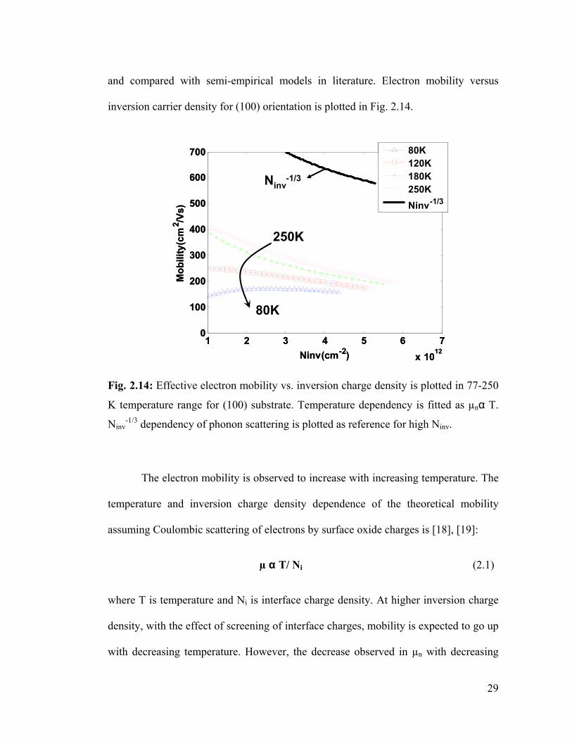
Fig. 2.14: Effective electron mobility vs. inversion charge density is plotted in 77-250
K temperature range for (100) substrate. Temperature dependency is fitted as µnα T.
Ninv-1/3 dependency of phonon scattering is plotted as reference for high Ninv............. 29
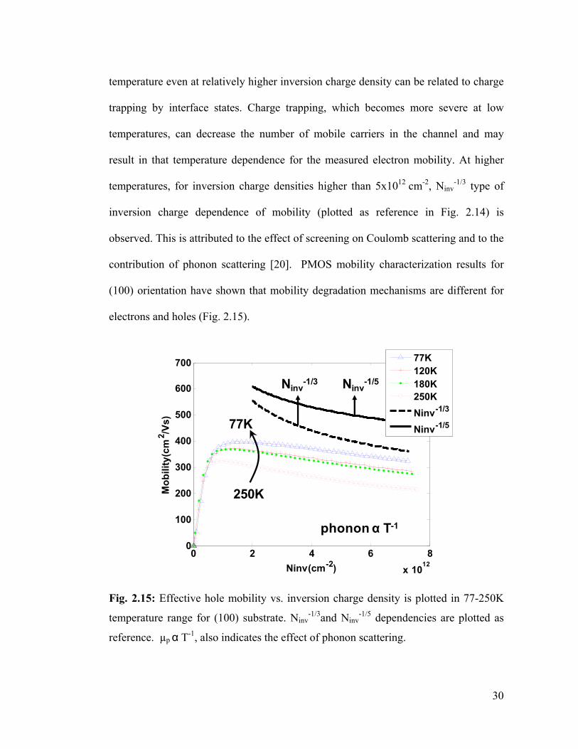
Fig. 2.15: Effective hole mobility vs. inversion charge density is plotted in 77-250K
temperature range for (100) substrate. Ninv-1/3and Ninv
-1/5 dependencies are plotted as
reference. µp α T-1, also indicates the effect of phonon scattering. ............................. 30
Fig. 2.16: Effective electron mobility vs. inversion charge density is plotted in 77-
250K temperature range for (111) substrate. µn increases with increasing temperature,
similar to (100) case. .................................................................................................... 33
Fig. 2.17: Effective hole mobility vs. inversion charge density is plotted in 77-250K
temperature range for (111) substrate. Mobility values and temperature & inversion
charge density dependencies look quite similar to (100) case, which also indicates that
phonon scattering is the dominant mechanism. ............................................................ 34
Chapter 3 Fig. 3.1: Theoretical high frequency (left figure) and theoretical low frequency
capacitance curves with and without Dit [12]. .............................................................. 42
xiv
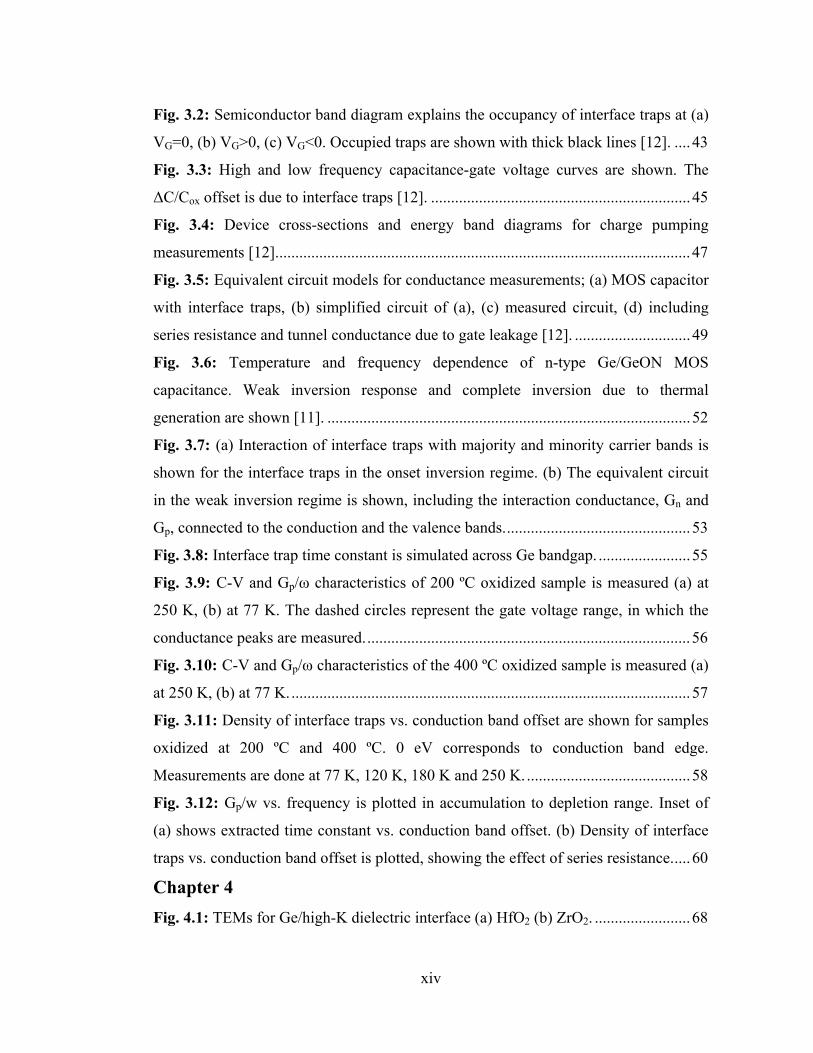
Fig. 3.2: Semiconductor band diagram explains the occupancy of interface traps at (a)
VG=0, (b) VG>0, (c) VG<0. Occupied traps are shown with thick black lines [12]. .... 43
Fig. 3.3: High and low frequency capacitance-gate voltage curves are shown. The
ΔC/Cox offset is due to interface traps [12]. ................................................................. 45
Fig. 3.4: Device cross-sections and energy band diagrams for charge pumping
measurements [12]. ....................................................................................................... 47
Fig. 3.5: Equivalent circuit models for conductance measurements; (a) MOS capacitor
with interface traps, (b) simplified circuit of (a), (c) measured circuit, (d) including
series resistance and tunnel conductance due to gate leakage [12]. ............................. 49
Fig. 3.6: Temperature and frequency dependence of n-type Ge/GeON MOS
capacitance. Weak inversion response and complete inversion due to thermal
generation are shown [11]. ........................................................................................... 52
Fig. 3.7: (a) Interaction of interface traps with majority and minority carrier bands is
shown for the interface traps in the onset inversion regime. (b) The equivalent circuit
in the weak inversion regime is shown, including the interaction conductance, Gn and
Gp, connected to the conduction and the valence bands. .............................................. 53
Fig. 3.8: Interface trap time constant is simulated across Ge bandgap. ....................... 55
Fig. 3.9: C-V and Gp/ω characteristics of 200 ºC oxidized sample is measured (a) at
250 K, (b) at 77 K. The dashed circles represent the gate voltage range, in which the
conductance peaks are measured. ................................................................................. 56
Fig. 3.10: C-V and Gp/ω characteristics of the 400 ºC oxidized sample is measured (a)
at 250 K, (b) at 77 K. .................................................................................................... 57
Fig. 3.11: Density of interface traps vs. conduction band offset are shown for samples
oxidized at 200 ºC and 400 ºC. 0 eV corresponds to conduction band edge.
Measurements are done at 77 K, 120 K, 180 K and 250 K. ......................................... 58
Fig. 3.12: Gp/w vs. frequency is plotted in accumulation to depletion range. Inset of
(a) shows extracted time constant vs. conduction band offset. (b) Density of interface
traps vs. conduction band offset is plotted, showing the effect of series resistance. .... 60
Chapter 4 Fig. 4.1: TEMs for Ge/high-K dielectric interface (a) HfO2 (b) ZrO2. ........................ 68

xv
Fig. 4.2: Interface state density extracted by quasi-CV technique (a) p-type (b) n-type
Ge substrates [12]. ........................................................................................................ 69
Fig. 4.3: Interface state density extracted by conducatnce technique, showing very
asymmetric distribution across Ge bandgap [19]. ........................................................ 70
Fig. 4.4: Cross sectional TEM (a) without sulfur passivation, (b) with sulfur
passivation. (c) Interface state density extracted by conductance technique, showing
poor electrical quality [20]. .......................................................................................... 71
Fig. 4.5: (a) SIMS profile for TaN/HfO2/GeOx/Ge gate stack. (b) Interface state
density reduction with fluorine treatment [25]. ............................................................ 72
Fig. 4.6: Schematic of ALD system, showing the gas flows and other chamber
elements. ....................................................................................................................... 74
Fig. 4.7: Gas diagram of ALD system ......................................................................... 75
Fig. 4.8: Dit distribution for samples ozone-oxidized in the 200-450°C range is shown
(legend). Legend shows ozone oxidation temperature and the insulator deposited at the
top of grown GeO2. Conductance is measured at 77,120,180 and 250 K to cover the
bandgap. ........................................................................................................................ 77
Fig. 4.9: Dit distribution for samples ozone-oxidized at 400°C and NH3 nitrided at
600°C. One order of magnitude decrease in Dit is achieved by moving from high
temperature nitridation in RTP system to low temperature ozone oxidation in ALD
system. .......................................................................................................................... 78
Fig. 4.10: GeOx suboxide layer between Ge substrate and GeO2 is shown. ................ 79
Fig. 4.11: Dit dependency on oxide growth temperature. ............................................ 80
Fig. 4.12: Ge 3d spectra obtained with synchrotron radiation at 400 eV are shown. 3d
spectrum after DI water etch of 400 °C sample confirms that the grown oxide was
GeO2. ............................................................................................................................ 81
Fig. 4.13: Ge 3d spectra obtained with synchrotron radiation at 600 eV are shown. The
shift of oxide peak towards lower binding energies with increasing growth temperature
(from 450 to 500 ºC) indicates the transformation of 4+ state to 2+ state. .................. 82
Fig. 4.14: Ge 3d spectrum is measured and fitting analyses are done. Main oxide peak
and interfacial oxide is decomposed to oxidation states. Intensities are compared to
xvi
bulk Ge peak. (a) Oxide grown at 400° C has mainly 4+ state and less intermediate
states while (b) oxide grown at 350° C has significant 3+ state and other intermediate
states. ............................................................................................................................ 83
Fig. 4.15: Ge 3d spectra of in-situ vacuum annealed-GeO2 ......................................... 84
Fig. 4.16: Ge 3d spectra of in-situ vacuum annealed-GeO2 ......................................... 86
Fig. 4.17: (a) C-V without forming gas anneal (b) C-V with forming gas anneal ....... 87
Fig. 4.18: Dit distribution for GeO2 and GeON samples. ............................................. 88
Fig. 4.19: (a) O 1s loss energy spectrum is shown. Bandgap of GeO2 is measured as
~5.1eV. (b) Ge 3d spectra obtained with synchrotron radiation before and after oxide
removal is shown. GeO2 is removed by in-situ annealing at 700 °C. (c) Valence band
spectra of GeO2 and oxide free surface are shown. Valence band offset of GeO2 is
measured as ~3.8 eV, while conduction band offset is only ~0.6eV. .......................... 89
Fig. 4.20: Dit distribution of samples treated under various thermal conditions [45]. . 90
Fig. 4.21: (a) Growth kinetics [50] (b) Dit for high pressure oxidation [51]. ............... 90
Chapter 5 Fig. 5.1: Inversion hole and electron mobilities of MOSFETs fabricated with (a) with
Al2O3 [3], (b) with HfO2 [4]. ...................................................................................... 102
Fig. 5.2: Inversion hole and electron mobilities (a) with GeON/SiO2 [5], (b) with
GeON/HfO2 [6]. ......................................................................................................... 102
Fig. 5.3: Ge N-MOSFET fabrication process flow is summarized. ........................... 104
Fig. 5.4: SIMS profile of P implanted in (100) Ge, activated in the 300-400 ºC range.
Junction depth is approximetely 100 nm. .................................................................. 105
Fig. 5.5: I-V characteristics of n+/p diodes activated at different conditions. Annealing
at lower temperatures provides excellent on/off ratio. Annealing in nitrogen or
forming gas environment does not affect I-V characteristics. .................................... 105
Fig. 5.6: Measured transfer characteristics of Ge (100) P-MOSFETs. ...................... 106
Fig. 5.7: Measured transfer characteristics of Ge (a) (100) N-MOSFETs, (b) (111) N-
MOSFETs. .................................................................................................................. 106
Fig. 5.8: Effective PMOS mobility is ~2.5 X of universal Si. No series resistance or
trapped charge corrections are done. .......................................................................... 107
xvii
Fig. 5.9: Effective NMOS (100) mobility, measured by split CV, shows 30%
improvement with the decrease in Dit but still lower than universal Si mobility. No
series resistance or trapped charge corrections are done. ........................................... 107
Fig. 5.10: The measureable window of Ge bandgap by conductance technique applied
at NMOS and PMOS inversion regimes. ................................................................... 109
Fig. 5.11: (a) Conductance peak response for PMOS inversion regime. Two sets of
conductance peaks, corresponding to two types of traps, are observed. (b) Time
constants of two distinct traps are measured. ............................................................. 109
Fig. 5.12: (a) Conductance peak response for NMOS inversion regime. Only single
type of trap behavior is observed. (b) Time constant of traps is measured. ............... 110
Fig. 5.13: Conductance peak response in different gate bias ranges (a) 77 K and (b)
180 K. As temperature is increased to 120 K and 180 K, the trap range visible in 1
kHz-1 MHz shifts away from valence band toward midgap and the conductance peaks
shift to corresponding gate biases. .............................................................................. 111
Fig. 5.14: Time constants vs. conductance band offset. In the legend A and B
correspond to distinct surface states. B states (closer valence band edge and smaller
capture cross section) can be correlated to donor-like states. A states (~0.1 eV away
from B states and larger capture cross section) can be correlated to acceptor-like
states. Solid lines are the simulated time constants for corresponding band gap
energies. ...................................................................................................................... 112
Fig. 5.15: CNL level is located ~0.1eV from valence band edge. Grey region
corresponds to occupied traps. (a) Net charge built up at interface is close to zero for
Ge PMOS. (b) Negative charge builds up at interface for Ge NMOS, due to acceptor
type of traps below Fermi level. Acceptor traps consumes electrons from inversion
layer. ........................................................................................................................... 114
Fig. 5.16: Dit vs bandgap for MOSFETs fabricated using GeO2 (400 oC) and GeON
(600 oC). Area under Dit distribution gives the total number of trapped charge. ....... 115
Fig. 5.17: Schematic explains the slow traps located at the interfacial oxide/high-K
border and in the bulk of high-K dielectric. ............................................................... 116
xviii
Fig. 5.18: Schematic explains the effect of low conductance band offset on electron
trapping by slow traps and bulk traps in NMOS inversion regime. ........................... 117
Fig. 5.19: Full C-V measurements are carried out on (a) PMOS and (b) NMOS. Both
cases hysteresis shows a positive Vfb shift once positive gate biases are applied. That
confirms the existence of slow electron traps. ............................................................ 117
Fig. 5.20: (a) Gate sweep is extended to ±4V. Vfb shift is measured as a function of
extent of Vg sweep. NMOS inversion shows ~+1.1V Vfb shift while PMOS inversion
shows only ~-0.2V. (b) Amount of trapped charge versus Vg-Vth is plotted. For NMOS
trapped charge reaches to 6x1012 cm-2 levels. ............................................................ 118
Fig. 5.21: Drain current gate voltage characteristics of PMOS are plotted. -4V of gate
voltage stress is applied for 1 min and total Vth shift is ~100-200 mV. ..................... 119
Fig. 5.22: Drain current gate voltage characteristics of (a) NMOS (100) and (b)
NMOS (111) are plotted for initial, +4V 1 min stressed and -4V 1 min stressed
transistors. Fig. (a) shows that the electrons trapped during +4V 1 min stress can be
detrapped by applying -4V stress for 1 min. Fig (b) shows that the electrons trapped
during +4V 1 min stress can be partially detrapped by applying -4V stress for 1 min.
.................................................................................................................................... 119
Fig. 5.23: Components of parasitic S/D resistance .................................................... 120
Fig. 5.24: Gated Hall devices are fabricated along with N-MOSFETs. Measuring drain
potential drop across the channel using additional voltage contacts eliminates the
effect of S/D series resistance. .................................................................................... 122
Fig. 5.25: Effective mobility is measured on short channel Ge NMOS (111) and gated
Hall devices fabricated on the same substrate. Eliminating S/D resistance significantly
increases the measured mobility. ................................................................................ 123
Fig. 5.26: Carrier concentration measured with SRP in S/D region of (111) Ge
NMOS. ........................................................................................................................ 124
Fig. 5.27: (a) Inversion carrier density and mobility are measured by Hall effect on Ge
NMOS (111). Ninv-Hall represents only mobile charge density in the channel. (b) Hall
mobility versus temperature is shown for constant gate bias voltage in (111) Ge
NMOS. ........................................................................................................................ 124
xix
Fig. 5.28: Conductivity tensors as a function of magnetic field (a) σxx. (b) σxy. ....... 126
Fig. 5.29: w/RS/D, w/Qtrappped, is measured on a short channel device where Rs/d
dominates. RS/D data is measured on gated Hall sample (Fig. 5.24), which eliminates
RS/D effect. Qtrapped corrected data is after trapped charge correction. Ninv, x-axis, is
measured by split-CV and corresponds to total charge, including trapped charge. ... 128
1
Chapter 1 Introduction
1.1 Motivation Since the first experimental demonstration in 1960 [1], Si-based Metal-Oxide-
Semiconductor-Field-Effect-Transistor (MOSFET) has become the driving force for
the semiconductor industry in the last four to five decades. Although the architecture
and working principle of the MOSFET have remained the same, the physical
dimensions have been continually reduced to double the number of transistors on a
chip every two years following Moore’s Law [2]. The exponential decrease in
transistor dimensions has resulted in increase in microprocessor performance over
technology generations. However, the conventional device dimension scaling cannot
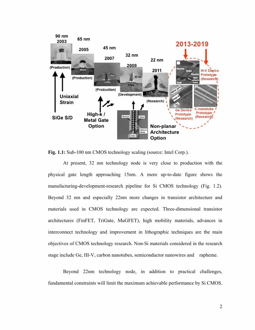
continue forever. As scaling reached sub-100nm regime, more non-silicon elements
were introduced to Si technology at every generation (Fig. 1.1). At 90nm node, SiGe
S/D was introduced to achieve uniaxial strain in the channel. That was followed by
integration of high-K metal gate at 45nm node, which is then called “The Biggest
Change in Transistor Technology in 40 Years” by Gordon Moore.
2
Fig. 1.1: Sub-100 nm CMOS technology scaling (source: Intel Corp.).
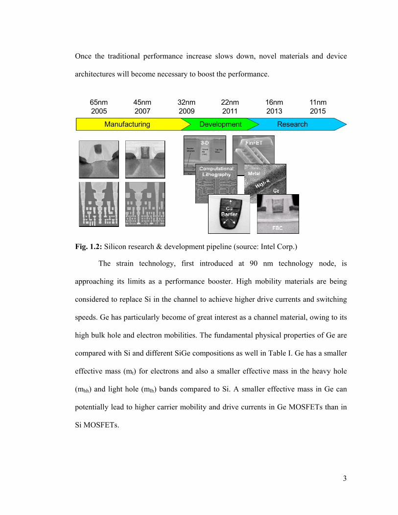
At present, 32 nm technology node is very close to production with the
physical gate length approaching 15nm. A more up-to-date figure shows the
manufacturing-development-research pipeline for Si CMOS technology (Fig. 1.2).
Beyond 32 nm and especially 22nm more changes in transistor architecture and
materials used in CMOS technology are expected. Three-dimensional transistor
architectures (FinFET, TriGate, MuGFET), high mobility materials, advances in
interconnect technology and improvement in lithographic techniques are the main
objectives of CMOS technology research. Non-Si materials considered in the research
stage include Ge, III-V, carbon nanotubes, semiconductor nanowires and �rapheme.
Beyond 22nm technology node, in addition to practical challenges,
fundamental constraints will limit the maximum achievable performance by Si CMOS.
3
Once the traditional performance increase slows down, novel materials and device
architectures will become necessary to boost the performance.
Fig. 1.2: Silicon research & development pipeline (source: Intel Corp.)
The strain technology, first introduced at 90 nm technology node, is
approaching its limits as a performance booster. High mobility materials are being
considered to replace Si in the channel to achieve higher drive currents and switching
speeds. Ge has particularly become of great interest as a channel material, owing to its
high bulk hole and electron mobilities. The fundamental physical properties of Ge are
compared with Si and different SiGe compositions as well in Table I. Ge has a smaller
effective mass (mt) for electrons and also a smaller effective mass in the heavy hole
(mhh) and light hole (mlh) bands compared to Si. A smaller effective mass in Ge can
potentially lead to higher carrier mobility and drive currents in Ge MOSFETs than in
Si MOSFETs.
65nm 45nm 32nm 22nm 16nm 11nm2005 2007 2009 2011 2013 2015
Manufacturing Development Research
4
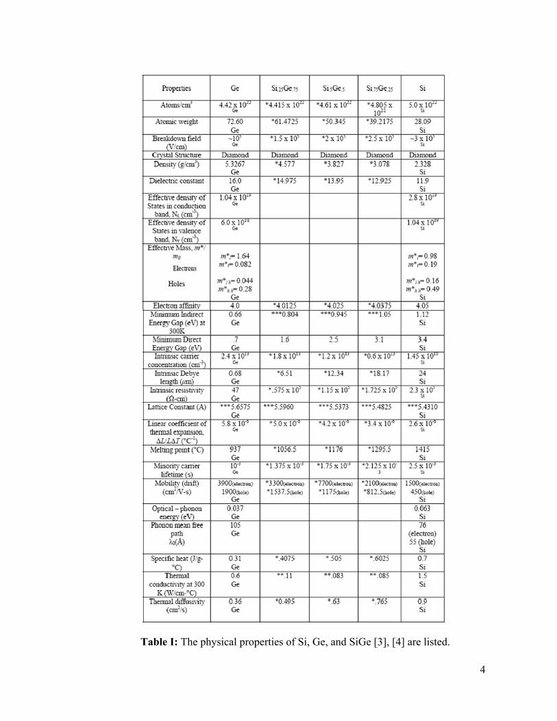
Table I: The physical properties of Si, Ge, and SiGe [3], [4] are listed.
5
In Table I, * value was derived through linear approximation; ** value was derived
through subjective observation of graph/diagram [3]; *** value was derived through
quadratic approximation.
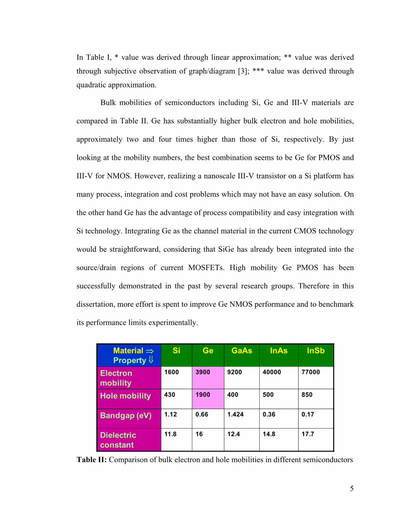
Bulk mobilities of semiconductors including Si, Ge and III-V materials are
compared in Table II. Ge has substantially higher bulk electron and hole mobilities,
approximately two and four times higher than those of Si, respectively. By just
looking at the mobility numbers, the best combination seems to be Ge for PMOS and
III-V for NMOS. However, realizing a nanoscale III-V transistor on a Si platform has
many process, integration and cost problems which may not have an easy solution. On
the other hand Ge has the advantage of process compatibility and easy integration with
Si technology. Integrating Ge as the channel material in the current CMOS technology
would be straightforward, considering that SiGe has already been integrated into the
source/drain regions of current MOSFETs. High mobility Ge PMOS has been
successfully demonstrated in the past by several research groups. Therefore in this
dissertation, more effort is spent to improve Ge NMOS performance and to benchmark
its performance limits experimentally.
Table II: Comparison of bulk electron and hole mobilities in different semiconductors
Material ⇒Property ⇓
Si Ge GaAs InAs InSb
Electron mobility
1600 3900 9200 40000 77000
Hole mobility 430 1900 400 500 850
Bandgap (eV) 1.12 0.66 1.424 0.36 0.17
Dielectric constant
11.8 16 12.4 14.8 17.7
6
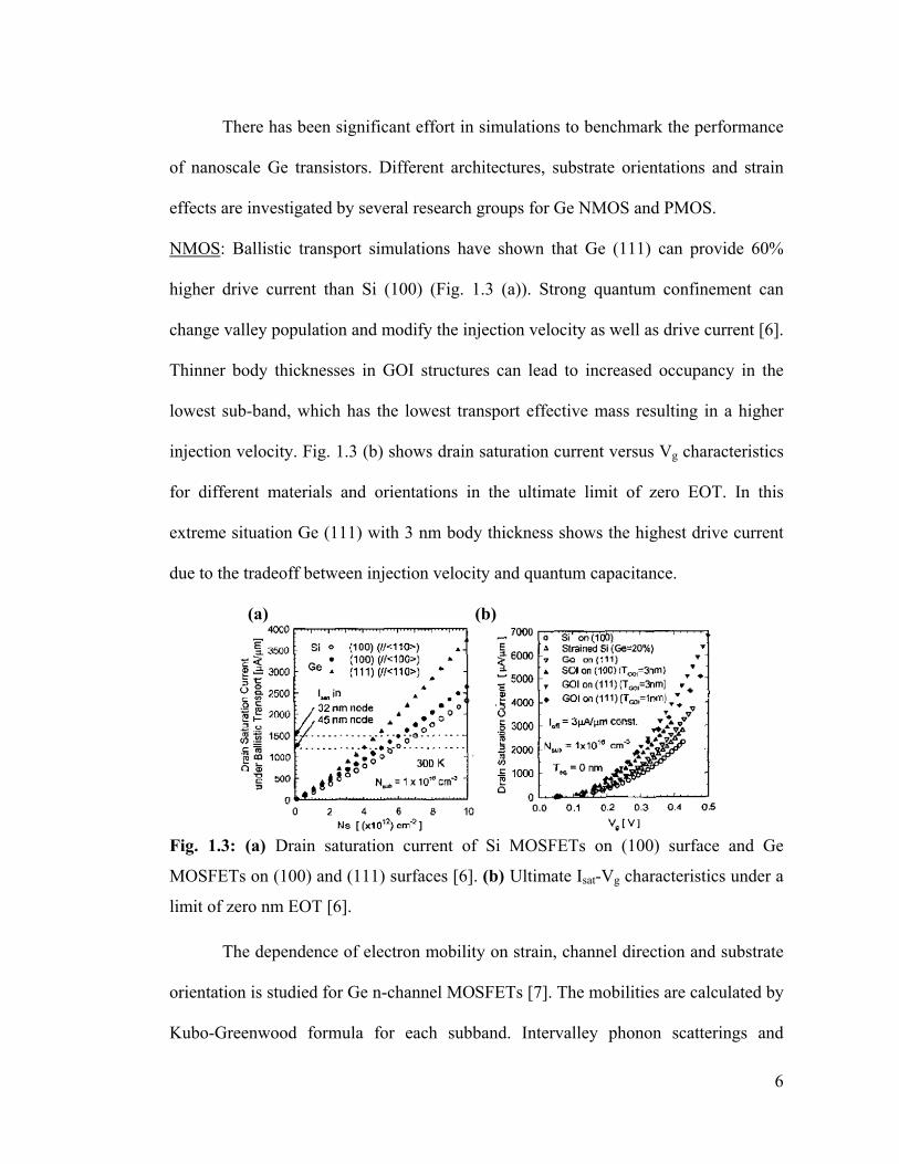
There has been significant effort in simulations to benchmark the performance
of nanoscale Ge transistors. Different architectures, substrate orientations and strain
effects are investigated by several research groups for Ge NMOS and PMOS.
NMOS: Ballistic transport simulations have shown that Ge (111) can provide 60%
higher drive current than Si (100) (Fig. 1.3 (a)). Strong quantum confinement can
change valley population and modify the injection velocity as well as drive current [6].
Thinner body thicknesses in GOI structures can lead to increased occupancy in the
lowest sub-band, which has the lowest transport effective mass resulting in a higher
injection velocity. Fig. 1.3 (b) shows drain saturation current versus Vg characteristics
for different materials and orientations in the ultimate limit of zero EOT. In this
extreme situation Ge (111) with 3 nm body thickness shows the highest drive current
due to the tradeoff between injection velocity and quantum capacitance.
(a) (b)
Fig. 1.3: (a) Drain saturation current of Si MOSFETs on (100) surface and Ge
MOSFETs on (100) and (111) surfaces [6]. (b) Ultimate Isat-Vg characteristics under a
limit of zero nm EOT [6].
The dependence of electron mobility on strain, channel direction and substrate
orientation is studied for Ge n-channel MOSFETs [7]. The mobilities are calculated by
Kubo-Greenwood formula for each subband. Intervalley phonon scatterings and
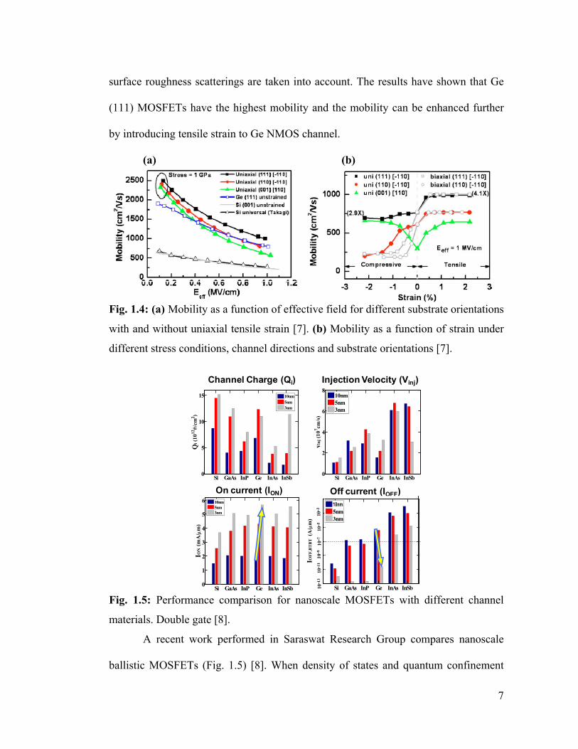
7
surface roughness scatterings are taken into account. The results have shown that Ge
(111) MOSFETs have the highest mobility and the mobility can be enhanced further
by introducing tensile strain to Ge NMOS channel.
(a) (b)
Fig. 1.4: (a) Mobility as a function of effective field for different substrate orientations
with and without uniaxial tensile strain [7]. (b) Mobility as a function of strain under
different stress conditions, channel directions and substrate orientations [7].
Fig. 1.5: Performance comparison for nanoscale MOSFETs with different channel
materials. Double gate [8].
A recent work performed in Saraswat Research Group compares nanoscale
ballistic MOSFETs (Fig. 1.5) [8]. When density of states and quantum confinement
Si GaAs InP Ge InAs InSb0
2
4
6
8
vinj
(107 cm
/s)
10nm5nm3nm
Si GaAs InP Ge InAs InSb0
5
10
15
Qi (
1012
#/cm
2 )
10nm5nm3nm
Channel Charge (Qi) Injection Velocity (Vinj)
Si GaAs InP Ge InAs InSb0
1
2
3
4
5
6
ION (m
A/ μ
m)
10nm5nm3nm
On current (ION)
Si GaAs InP Ge InAs InSb
IOFF
,BT
BT
(A/ μ
m)
10-1
310
-910
-710
-510
-310
-11
7nm5nm3nm
10nm
Off current (IOFF)
Si GaAs InP Ge InAs InSb
8
effects are taken into account, Si has the largest inversion charge density and the
inversion charge is reduced due to low DOS in III-V materials. Ge lies in between Si
and III-V materials in terms of inversion charge density. Injection velocity results
show that Si has the smallest injection velocity and III-V materials have the highest
because of low effective mass. Ge is again in between, better than Si but worse than
III-V materials in terms of injection velocity. Combining inversion charge and the
injection velocity, Ge shows the highest on current, especially for scaled body
thicknesses. According to off current simulation results, quantization helps Ge to
reduce BTBT leakage and meet the off current requirements.
PMOS: As opposed to NMOS, there have been encouraging experimental
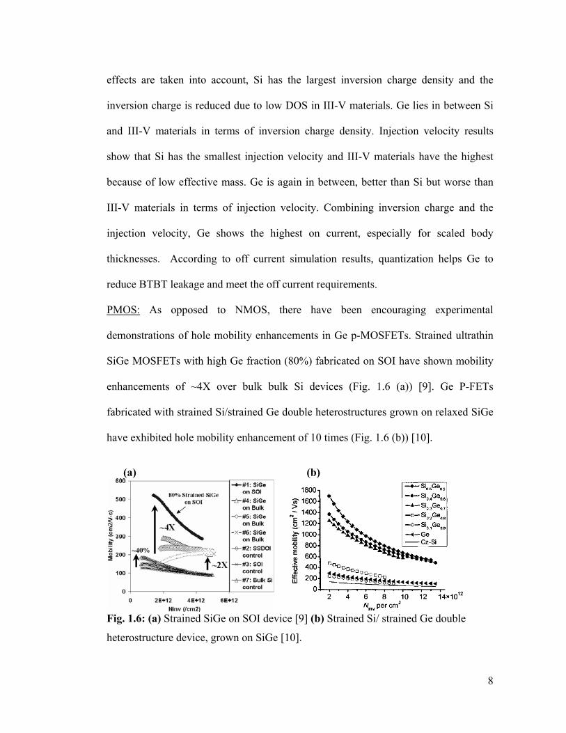
demonstrations of hole mobility enhancements in Ge p-MOSFETs. Strained ultrathin
SiGe MOSFETs with high Ge fraction (80%) fabricated on SOI have shown mobility
enhancements of ~4X over bulk bulk Si devices (Fig. 1.6 (a)) [9]. Ge P-FETs
fabricated with strained Si/strained Ge double heterostructures grown on relaxed SiGe
have exhibited hole mobility enhancement of 10 times (Fig. 1.6 (b)) [10].
(a) (b)
Fig. 1.6: (a) Strained SiGe on SOI device [9] (b) Strained Si/ strained Ge double
heterostructure device, grown on SiGe [10].
9
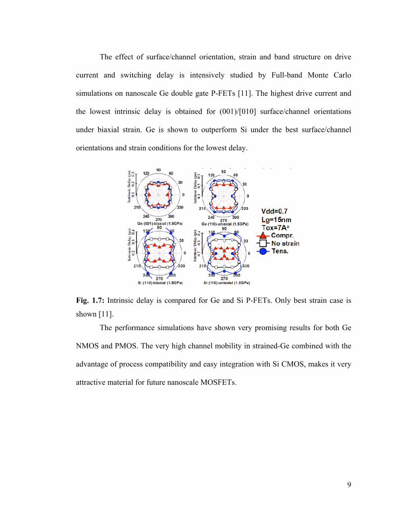
The effect of surface/channel orientation, strain and band structure on drive
current and switching delay is intensively studied by Full-band Monte Carlo
simulations on nanoscale Ge double gate P-FETs [11]. The highest drive current and
the lowest intrinsic delay is obtained for (001)/[010] surface/channel orientations
under biaxial strain. Ge is shown to outperform Si under the best surface/channel
orientations and strain conditions for the lowest delay.
Fig. 1.7: Intrinsic delay is compared for Ge and Si P-FETs. Only best strain case is
shown [11].
The performance simulations have shown very promising results for both Ge
NMOS and PMOS. The very high channel mobility in strained-Ge combined with the
advantage of process compatibility and easy integration with Si CMOS, makes it very
attractive material for future nanoscale MOSFETs.
10
1.2 Thesis Organization The objective of this work is to develop various advanced technologies to
fabricate high performance Ge CMOS. Two main issues targeted in the device level
are:
- High quality interface and gate dielectric stack development for Ge.
- Performance improvement in Ge NMOS.
This dissertation is organized as 6 chapters. Chapter 2 presents preliminary
results for Ge MOSFETs with GeON gate dielectric, discusses the effect
crystallographic orientation on Ge NMOS and PMOS mobility and examines the
carrier scattering mechanisms in Ge MOSFETs through electrical characterizations. A
brief review of interface characterization techniques in literature is given in Chapter 3.
The low temperature conductance technique is proposed for accurate characterization
of channel/gate-dielectric interface in Ge. Interface trap density distribution across Ge
bandgap is illustrated.
Surface passivation of Ge is a key challenge to achieve high performance Ge
MOSFETs. In Chapter 4, a novel technique is introduced to engineer Ge interface
and reduce the trap density. A high quality Ge/dielectric interface with low interface
trap density is presented. Electrical and structural characterizations and stability
analysis are discussed. Chapter 5 focuses on performance improvement in Ge NMOS.
The results on Ge NMOS devices fabricated with the interface engineering technique
are discussed. Detailed interface characterizations, trapping analyses and gated Hall
device measurements are elaborated in order to identify the mechanisms behind poor
Ge NMOS performance in the past.
11
Finally, Chapter 6 summarizes the conclusions and the contributions of this
work and recommends future research directions.
1.3 References [1] D. Kahng, M. M. Atalla, “Silicon-silicon dioxide field induced surface devices”,
IRE-AIEEE Solid State Device Research Conference (Carnegie Inst. Of Tech.,
Pittsburgh, PA), 1960.
[2] G. E. Moore, “Cramming more components onto integrated circuits”, Electronics,
vol. 38, pp. 114, 1965.
[3] S.M. Sze, Physics of Semiconductor Devices, John Wiley and Sons, Inc, New
York, 1981
[4] S. Wolf, R. Tauber, Silicon Processing for the VLSI Era, Lattice Press, Sunset
Beach, California, 1986.
[5] E. Kasper, Properties of Strained and Relaxed Silicon Germanium, INSPEC,
London, 1995.
[6] S. Takagi, “Re-examination of subband structure engineering in ultra-short
channel MOSFETs under ballistic carrier transport”, VLSI Symp. Digest, pp. 115,
2003.
[7] Y.-J. Yang, W. S. Ho, C.–F. Huang, S. T. Chang, C. W. Liu, “Electron mobility
enhancement in strained-germanium n-channel metal-oxide-semiconductor field-
effect transistors”, Appl. Phys. Lett., vol. 91, pp. 102103 (2007).
[8] D. Kim, T. Krishnamohan, K. C. Saraswat, “Performance evaluation of III-V
double gate n-MOSFETs”, IEEE DRC Digest, pp. 67, 2008.
12
[9] T. Krishnamohan, Z. Krivokapic, K. Uchida, Y. Nishi, K. C. Saraswat, “High-
mobility ultrathin strained Ge MOSFETs on bulk and SOI with low band-to-band
tunneling leakage: Experiments”, IEEE Trans. Elect. Dev., vol. 53, pp. 990, 2006.
[10] M. L. Lee, E. A. Fitzgerald, “Optimized strained Si/strained Ge dual-channel
heterostructures for high mobility P- and N-MOSFETs”, IEDM Tech. Dig., pp.
429, 2003.
[11] T. Krishnamohan, D. Kim, T. V. Dinh, A. Pham, B. Meinerzhagen, C.
Jungemann, K. Saraswat, “Comparison of (001), (110) and (111) Uniaxial- and
Biaxial- Strained-Ge and Strained-Si PMOS DGFETs for All Channel
orientations: Mobility Enhancement, Drive Current, Delay and Off-State
Leakage”, IEDM Tech. Dig., 2008.

13
14
Chapter 2 Ge MOSFETS
2.1 Introduction Future CMOS scaling requires introduction of new channel materials and
innovative device structures [1]. Recently, Ge has become of great interest as a
channel material for future technology nodes, owing to its bulk electron and hole
mobilities that are two and four times higher than those of Si, respectively. Ge has a
small hole conductivity effective mass and hence can achieve higher inversion hole
mobility. High density of states (DOS) of Ge allows for it to support channel charge
in its higher mobility valleys even with strong quantization attributed either to the
spatial quantum confinement or to the high electric field. This makes Ge an attractive
channel material for future high-performance N-MOSFETs. However, replacement of
Si channel by Ge in these devices requires alternative processing methods at various
steps in device fabrication. Two major challenges in realizing Ge MOS technology are
surface passivation and n-type dopant activation.
Ge MOSFETs with different gate dielectrics including HfO2 [2], ZrO2 [3],
Al2O3 [4], LaAlO3 [5], GeON [6] have been demonstrated. Mobilities above 300cm2V-
15
1s-1 have been reported for Ge PMOS [6]. However, Ge NMOS has exhibited poor
drive current and low mobility, as reported by several different research groups
worldwide [7], [8]. Detailed characterization of gate oxide/channel interface and a
deeper understanding of mobility degradation mechanisms are needed to address the
Ge NMOS performance problem.
In this chapter, the details of Ge MOSFET fabrication techniques are
presented. The Ge-GeON interface is investigated using the conductance technique at
low temperatures to extract an accurate distribution of interface traps (Dit) across the
bandgap of Ge. Diode characteristics and non-idealities of the source/drain junctions
of the Ge- MOSFETs are illustrated. The experimental findings on the effects of
substrate crystallographic orientation on electron mobility (µn) and hole mobility (µp)
are discussed. The 50% improvement in µn for the (111) orientation over (100)
orientation is explained based on both measurements and band structure theory.
Carrier scattering mechanisms and their effects on µn and µp are studied through low
temperature measurements and the results are correlated with the interface studies.
2.2 Ge MOSFET Fabrication The MOSFET fabrication process flow is summarized in Table I. N- and P-
type, 100 mm diameter, very lightly doped (~1014 cm3), Ge substrates with (100) and
(111) surface orientations supplied by UMICORE were used as starting materials. The
first part of the process involved the formation of the field isolation dielectric
consisting of GeOxNy formation and SiO2 deposition. A modified pre-diffusion clean,
including surface organics removal in addition to oxide removal by cyclic- HF clean
[10], was used for these substrates. The removal of surface organics was done by
16
washing the wafers in PRS-1000 at 45 °C for 10 min followed by DI water dump rinse
and a spin dry. The native oxides of Ge were removed by dipping the wafers in DI
water. The sub-oxides, which cannot be removed in DI water etching, were etched by
dipping the wafers in 2% HF solution for 30 s. A cyclic clean involving treating the
wafers with DI water and 2% HF successively was employed 3 times to remove most
of the oxides on the surface. The wafers were then immediately loaded in a rapid
thermal processing (RTP) system for oxynitridation. This process was accomplished in
two steps, first a short oxidation of the Ge at 600 °C for 5 s in dry O2 followed by a
long purge of the system in N2. This was followed by a nitriding step accomplished by
annealing the wafers in an NH3 environment at 600 °C for 3 min. The wafers were
then loaded into a CVD system to deposit SiO2 using SiH4 and O2 at 400 °C. Active
area lithography was done and the field stack was then etched in a 20:1 Buffered
Oxide Etch solution. Subsequently, photoresist was stripped in O2 plasma.
The modified pre-diffusion clean described above was performed again on
these wafers followed by the same oxynitridation process to form the GeOxNy gate
dielectric. A cap layer of CVD SiO2 was used to reduce the leakage current density
across the gate stack. This oxide was deposited at a slightly higher temperature of
450 °C and a reduced pressure of 200 mT compared to the isolation oxide deposition.
Poly-Si0.4Ge0.6 was employed as the gate electrode. SiH4 and GeH4 were used as
source gases for the CVD gate deposition, which was done at 400 °C and 400 mT. The
gate was patterned using an anisotropic dry etch, achieving good selectivity between
the poly-SiGe and the SiO2.
17
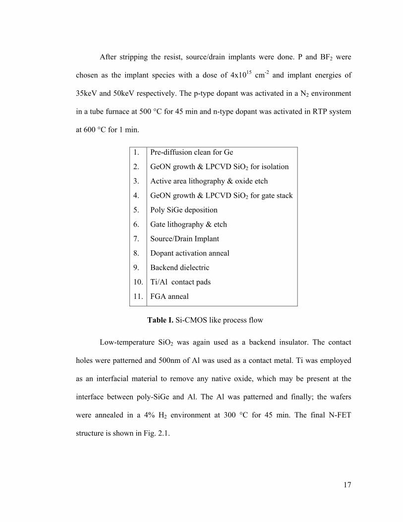
After stripping the resist, source/drain implants were done. P and BF2 were
chosen as the implant species with a dose of 4x1015 cm-2 and implant energies of
35keV and 50keV respectively. The p-type dopant was activated in a N2 environment
in a tube furnace at 500 °C for 45 min and n-type dopant was activated in RTP system
at 600 °C for 1 min.
Table I. Si-CMOS like process flow
Low-temperature SiO2 was again used as a backend insulator. The contact
holes were patterned and 500nm of Al was used as a contact metal. Ti was employed
as an interfacial material to remove any native oxide, which may be present at the
interface between poly-SiGe and Al. The Al was patterned and finally; the wafers
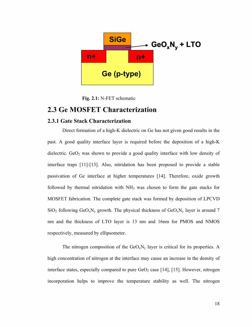
were annealed in a 4% H2 environment at 300 °C for 45 min. The final N-FET
structure is shown in Fig. 2.1.
1.
2.
3.
4.
5.
6.
7.
8.
9.
10.
11.
Pre-diffusion clean for Ge
GeON growth & LPCVD SiO2 for isolation
Active area lithography & oxide etch
GeON growth & LPCVD SiO2 for gate stack
Poly SiGe deposition
Gate lithography & etch
Source/Drain Implant
Dopant activation anneal
Backend dielectric
Ti/Al contact pads
FGA anneal
18
Fig. 2.1: N-FET schematic
2.3 Ge MOSFET Characterization 2.3.1 Gate Stack Characterization Direct formation of a high-K dielectric on Ge has not given good results in the
past. A good quality interface layer is required before the deposition of a high-K
dielectric. GeO2 was shown to provide a good quality interface with low density of
interface traps [11]-[13]. Also, nitridation has been proposed to provide a stable
passivation of Ge interface at higher temperatures [14]. Therefore, oxide growth
followed by thermal nitridation with NH3 was chosen to form the gate stacks for
MOSFET fabrication. The complete gate stack was formed by deposition of LPCVD
SiO2 following GeOxNy growth. The physical thickness of GeOxNy layer is around 7
nm and the thickness of LTO layer is 13 nm and 16nm for PMOS and NMOS
respectively, measured by ellipsometer.
The nitrogen composition of the GeOxNy layer is critical for its properties. A
high concentration of nitrogen at the interface may cause an increase in the density of
interface states, especially compared to pure GeO2 case [14], [15]. However, nitrogen
incorporation helps to improve the temperature stability as well. The nitrogen
Ge (p-type)
n+n+
SiGe GeOxNy + LTO
Ge (p-type)
n+n+
SiGe GeOxNy + LTO
19
composition of the grown GeOxNy layer was determined to be 17% at the interface
using angle-resolved x-ray photoemission spectroscopy (AR-XPS).
The capacitance-voltage (C-V) characteristics obtained from Ge p- and n-FETs
with (100) orientation are shown in Fig. 2.2 and 2.3. C-V characteristics were
measured in 1 kHz-1MHz frequency range at 250K. Time constants for capture and
emission processes of carriers through interface traps are much shorter for Ge than for
Si, due to smaller bandgap. Cooling down to 250K helps to prevent inversion
response via thermal generation in the bulk region. It is noteworthy that C-V’s were
measured on final MOSFET structures after going through several annealing steps as
explained in device fabrication section above. C-V hysteresis was less than 100 mV
for both NMOS and PMOS. C-V characteristics for NMOS (p-substrate) correspond to
Ge surface potential in the lower half of the bandgap, which is closer to valence band
(Ev), where the depletion takes place for the p-type substrate. C-V characteristics
measured for PMOS (n-substrate) correspond to the upper half of the bandgap, closer
to conduction band (Ec). Larger frequency dispersion was observed (e.g. a kink at low
frequencies in the depletion region) for n-type substrates (Fig. 2.3)). A high density of
interface states in the upper half of the bandgap can be responsible for the larger
frequency dispersion in n-type substrate; this possibility was investigated through Dit
measurements in this work.
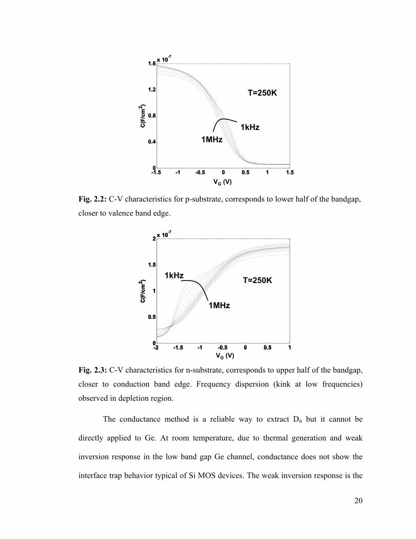
20
Fig. 2.2: C-V characteristics for p-substrate, corresponds to lower half of the bandgap,
closer to valence band edge.
Fig. 2.3: C-V characteristics for n-substrate, corresponds to upper half of the bandgap,
closer to conduction band edge. Frequency dispersion (kink at low frequencies)
observed in depletion region.
The conductance method is a reliable way to extract Dit but it cannot be
directly applied to Ge. At room temperature, due to thermal generation and weak
inversion response in the low band gap Ge channel, conductance does not show the
interface trap behavior typical of Si MOS devices. The weak inversion response is the
-1.5 -1 -0.5 0 0.5 1 1.50
0.4
0.8
1.2
1.6 x 10⁻⁷
Vg(V)
C(F
/cm
2 )
T=250K
1MHz1kHz
VG (V)-1.5 -1 -0.5 0 0.5 1 1.50
0.4
0.8
1.2
1.6 x 10⁻⁷
Vg(V)
C(F
/cm
2 )
T=250K
1MHz1kHz
VG (V)
-2 -1.5 -1 -0.5 0 0.5 10
0.5
1
1.5
2 x 10⁻⁷
Vg(V)
C(F
/cm
2 ) 1kHz
1MHz
T=250K
VG (V)-2 -1.5 -1 -0.5 0 0.5 10
0.5
1
1.5
2 x 10⁻⁷
Vg(V)
C(F
/cm
2 ) 1kHz
1MHz
T=250K
-2 -1.5 -1 -0.5 0 0.5 10
0.5
1
1.5
2 x 10⁻⁷
Vg(V)
C(F
/cm
2 ) 1kHz
1MHz
T=250K
VG (V)
21
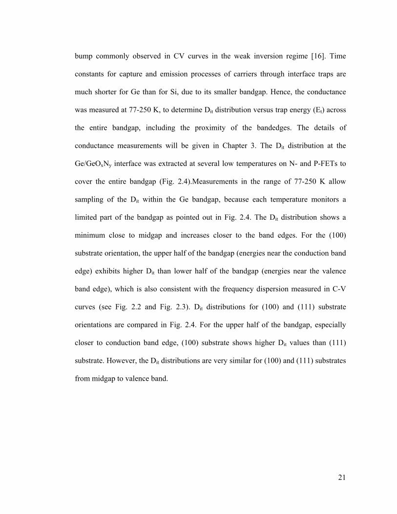
bump commonly observed in CV curves in the weak inversion regime [16]. Time
constants for capture and emission processes of carriers through interface traps are
much shorter for Ge than for Si, due to its smaller bandgap. Hence, the conductance
was measured at 77-250 K, to determine Dit distribution versus trap energy (Et) across
the entire bandgap, including the proximity of the bandedges. The details of
conductance measurements will be given in Chapter 3. The Dit distribution at the
Ge/GeOxNy interface was extracted at several low temperatures on N- and P-FETs to
cover the entire bandgap (Fig. 2.4).Measurements in the range of 77-250 K allow
sampling of the Dit within the Ge bandgap, because each temperature monitors a
limited part of the bandgap as pointed out in Fig. 2.4. The Dit distribution shows a
minimum close to midgap and increases closer to the band edges. For the (100)
substrate orientation, the upper half of the bandgap (energies near the conduction band
edge) exhibits higher Dit than lower half of the bandgap (energies near the valence
band edge), which is also consistent with the frequency dispersion measured in C-V
curves (see Fig. 2.2 and Fig. 2.3). Dit distributions for (100) and (111) substrate
orientations are compared in Fig. 2.4. For the upper half of the bandgap, especially
closer to conduction band edge, (100) substrate shows higher Dit values than (111)
substrate. However, the Dit distributions are very similar for (100) and (111) substrates
from midgap to valence band.
22
Fig. 2.4: Dit vs. trap energy (Et) in Ge bandgap for MOSFETs fabricated on (100) and
(111) substrates for 77K-250K temperature range. Dit is extracted for the same devices
used in mobility characterization. N-substrate (PMOS) is used for the upper half of the
bandgap while p-substrate (NMOS) is used for the lower half. Entire bandgap is
covered with measurements done at 77,180 and 250 K.
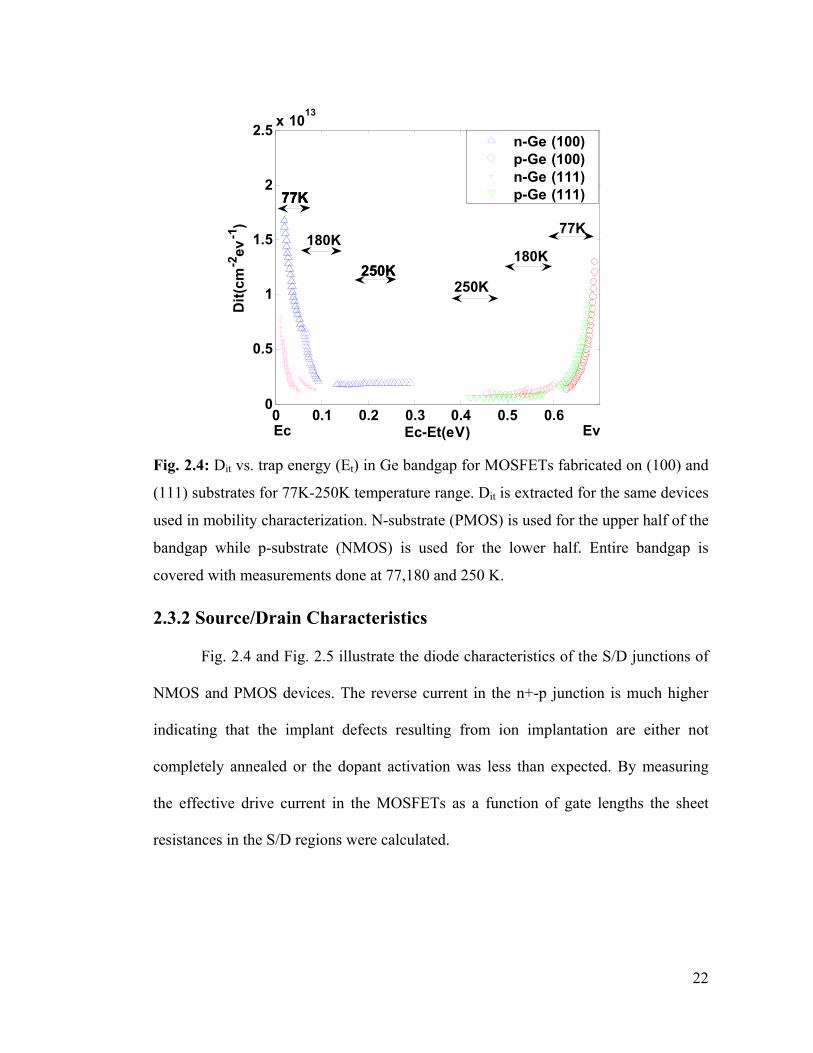
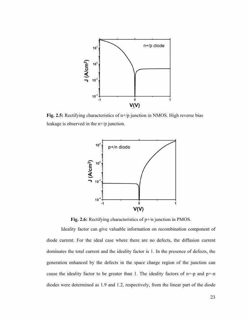
2.3.2 Source/Drain Characteristics
Fig. 2.4 and Fig. 2.5 illustrate the diode characteristics of the S/D junctions of
NMOS and PMOS devices. The reverse current in the n+-p junction is much higher
indicating that the implant defects resulting from ion implantation are either not
completely annealed or the dopant activation was less than expected. By measuring
the effective drive current in the MOSFETs as a function of gate lengths the sheet
resistances in the S/D regions were calculated.
0 0.1 0.2 0.3 0.4 0.5 0.60
0.5
1
1.5
2
2.5 x 10¹³
Ec-Et(eV)
Dit(
cm-2
ev-1
)
n-Ge (100)p-Ge (100)n-Ge (111)p-Ge (111)77K77K77K
180K
250K
Ec Ev
250K250K
180K
77K
23
Fig. 2.5: Rectifying characteristics of n+/p junction in NMOS. High reverse bias
leakage is observed in the n+/p junction.
Fig. 2.6: Rectifying characteristics of p+/n junction in PMOS.
Ideality factor can give valuable information on recombination component of
diode current. For the ideal case where there are no defects, the diffusion current
dominates the total current and the ideality factor is 1. In the presence of defects, the
generation enhanced by the defects in the space charge region of the junction can
cause the ideality factor to be greater than 1. The ideality factors of n+-p and p+-n
diodes were determined as 1.9 and 1.2, respectively, from the linear part of the diode
V(V)
J (A
/cm
2 )
V(V)
J (A
/cm
2 )J
(A/c
m2 )
V(V)
J (A
/cm
2 )
V(V)
24
I-V curves. The high ideality factor of n+-p diode is attributed to the implant defects
or insufficient dopant activation.
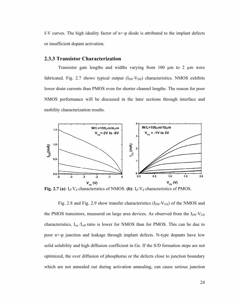
2.3.3 Transistor Characterization Transistor gate lengths and widths varying from 100 µm to 2 µm were
fabricated. Fig. 2.7 shows typical output (IDS-VDS) characteristics. NMOS exhibits
lower drain currents than PMOS even for shorter channel lengths. The reason for poor
NMOS performance will be discussed in the later sections through interface and
mobility characterization results.
Fig. 2.7 (a): Id-Vd characteristics of NMOS. (b): Id-Vd characteristics of PMOS.
Fig. 2.8 and Fig. 2.9 show transfer characteristics (IDS-VGS) of the NMOS and
the PMOS transistors, measured on large area devices. As observed from the IDS-VGS
characteristics, Ion /Ioff ratio is lower for NMOS than for PMOS. This can be due to
poor n+-p junction and leakage through implant defects. N-type dopants have low
solid solubility and high diffusion coefficient in Ge. If the S/D formation steps are not
optimized, the over diffusion of phosphorus or the defects close to junction boundary
which are not annealed out during activation annealing, can cause serious junction
I DS(
mA
)I D
S(m
A)
25
leakage. For short channel length transistors, they can even result in subsurface
conduction, degrading the Ion /Ioff ratio for Ge NMOS.
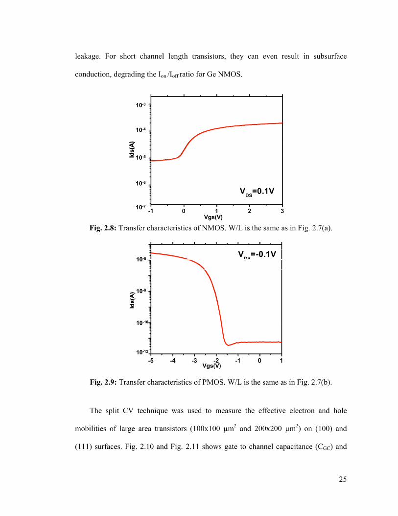
Fig. 2.8: Transfer characteristics of NMOS. W/L is the same as in Fig. 2.7(a).
Fig. 2.9: Transfer characteristics of PMOS. W/L is the same as in Fig. 2.7(b).
The split CV technique was used to measure the effective electron and hole
mobilities of large area transistors (100x100 µm2 and 200x200 µm2) on (100) and
(111) surfaces. Fig. 2.10 and Fig. 2.11 shows gate to channel capacitance (CGC) and
10-3
10-4
10-5
10-6
10-7
Vgs(V)
Ids(
A)
10-3
10-4
10-5
10-6
10-7
Vgs(V)
Ids(
A)
10-6
10-8
10-10
10-12
Vgs(V)
Ids(
A)
10-6
10-8
10-10
10-12
Vgs(V)
Ids(
A)
26
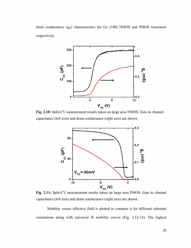
drain conductance (gD) characteristics for Ge (100) NMOS and PMOS transistors
respectively.
Fig. 2.10: Split-CV measurement results taken on large area NMOS. Gate to channel
capacitance (left axis) and drain conductance (right axis) are shown.
Fig. 2.11: Split-CV measurement results taken on large area PMOS. Gate to channel
capacitance (left axis) and drain conductance (right axis) are shown.
Mobility versus effective field is plotted to compare it for different substrate
orientations along with universal Si mobility curves (Fig. 2.12-13). The highest
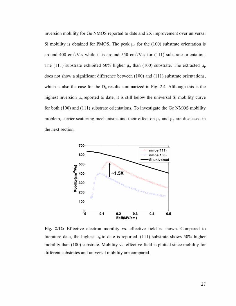
27
inversion mobility for Ge NMOS reported to date and 2X improvement over universal
Si mobility is obtained for PMOS. The peak µn for the (100) substrate orientation is
around 400 cm2/V-s while it is around 550 cm2/V-s for (111) substrate orientation.
The (111) substrate exhibited 50% higher µn than (100) substrate. The extracted µp
does not show a significant difference between (100) and (111) substrate orientations,
which is also the case for the Dit results summarized in Fig. 2.4. Although this is the
highest inversion µn reported to date, it is still below the universal Si mobility curve
for both (100) and (111) substrate orientations. To investigate the Ge NMOS mobility
problem, carrier scattering mechanisms and their effect on µn and µp are discussed in
the next section.
Fig. 2.12: Effective electron mobility vs. effective field is shown. Compared to
literature data, the highest µn to date is reported. (111) substrate shows 50% higher
mobility than (100) substrate. Mobility vs. effective field is plotted since mobility for
different substrates and universal mobility are compared.
0 0.1 0.2 0.3 0.4 0.50
100
200
300
400
500
600
700
Eeff(MV/cm)
Mob
ility
(cm
2 /Vs)
nmos(111)nmos(100)Si universal
~1.5X
0 0.1 0.2 0.3 0.4 0.50
100
200
300
400
500
600
700
Eeff(MV/cm)
Mob
ility
(cm
2 /Vs)
nmos(111)nmos(100)Si universal
~1.5X
28
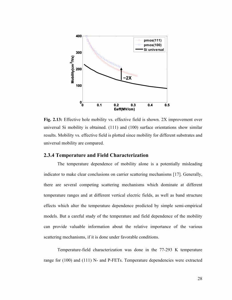
Fig. 2.13: Effective hole mobility vs. effective field is shown. 2X improvement over
universal Si mobility is obtained. (111) and (100) surface orientations show similar
results. Mobility vs. effective field is plotted since mobility for different substrates and
universal mobility are compared.
2.3.4 Temperature and Field Characterization The temperature dependence of mobility alone is a potentially misleading
indicator to make clear conclusions on carrier scattering mechanisms [17]. Generally,
there are several competing scattering mechanisms which dominate at different
temperature ranges and at different vertical electric fields, as well as band structure
effects which alter the temperature dependence predicted by simple semi-empirical
models. But a careful study of the temperature and field dependence of the mobility
can provide valuable information about the relative importance of the various
scattering mechanisms, if it is done under favorable conditions.
Temperature-field characterization was done in the 77-293 K temperature
range for (100) and (111) N- and P-FETs. Temperature dependencies were extracted
0 0.1 0.2 0.3 0.4 0.50
100
200
300
400
Eeff(MV/cm)
Mob
ility
(cm
2 /Vs)
pmos(111)pmos(100)Si universal
~2X
0 0.1 0.2 0.3 0.4 0.50
100
200
300
400
Eeff(MV/cm)
Mob
ility
(cm
2 /Vs)
pmos(111)pmos(100)Si universal
~2X
29
and compared with semi-empirical models in literature. Electron mobility versus
inversion carrier density for (100) orientation is plotted in Fig. 2.14.
Fig. 2.14: Effective electron mobility vs. inversion charge density is plotted in 77-250
K temperature range for (100) substrate. Temperature dependency is fitted as µnα T.
Ninv-1/3 dependency of phonon scattering is plotted as reference for high Ninv.
The electron mobility is observed to increase with increasing temperature. The
temperature and inversion charge density dependence of the theoretical mobility
assuming Coulombic scattering of electrons by surface oxide charges is [18], [19]:
µ α T/ Ni (2.1)
where T is temperature and Ni is interface charge density. At higher inversion charge
density, with the effect of screening of interface charges, mobility is expected to go up
with decreasing temperature. However, the decrease observed in µn with decreasing
1 2 3 4 5 6 7x 10¹²
0
100
200
300
400
500
600
700
Ninv(cm-2)
Mob
ility
(cm
2 /Vs)
80K120K180K250KNinv-1/3
80K
250K
Ninv-1/3
1 2 3 4 5 6 7x 10¹²
0
100
200
300
400
500
600
700
Ninv(cm-2)
Mob
ility
(cm
2 /Vs)
80K120K180K250KNinv-1/3
80K
250K
Ninv-1/3
30
temperature even at relatively higher inversion charge density can be related to charge
trapping by interface states. Charge trapping, which becomes more severe at low
temperatures, can decrease the number of mobile carriers in the channel and may
result in that temperature dependence for the measured electron mobility. At higher
temperatures, for inversion charge densities higher than 5x1012 cm-2, Ninv-1/3 type of
inversion charge dependence of mobility (plotted as reference in Fig. 2.14) is
observed. This is attributed to the effect of screening on Coulomb scattering and to the
contribution of phonon scattering [20]. PMOS mobility characterization results for
(100) orientation have shown that mobility degradation mechanisms are different for
electrons and holes (Fig. 2.15).
Fig. 2.15: Effective hole mobility vs. inversion charge density is plotted in 77-250K
temperature range for (100) substrate. Ninv-1/3and Ninv
-1/5 dependencies are plotted as
reference. µp α T-1, also indicates the effect of phonon scattering.
0 2 4 6 8x 10¹²
0
100
200
300
400
500
600
700
Ninv(cm-2)
Mob
ility
(cm
2 /Vs)
77K120K180K250KNinv-1/3
Ninv-1/5
Ninv-1/5Ninv
-1/3
250K
77K
phonon α T-1
31
In contrast to µn very little Coulomb degradation is observed in µp at very low fields.
This is consistent with higher Dit values extracted for the upper half of the bandgap
than for the lower half of the bandgap for GeOxNy passivated Ge (Fig. 2.4). For holes,
µp is inversely proportional to temperature, which indicates that dominant mechanism
is phonon scattering (Fig. 2.15) [21]. The theory of scattering for holes is more
complicated, including warped bands, intra and interband scattering. Also semi-
empirical mobility models are not as simple for holes as for electron mobility case. In
general, mobility limited by phonon scattering is empirically modeled as:
µph α T-n Ninv-1/β (2.2)
where T is temperature and Ninv is inversion charge density. But hole mobility does
not typically exhibit a single power law over Ninv [21]. β is not constant in the
temperature range and electric field investigated. The mobility limited by acoustic
phonon scattering is modeled as µac α T-1 Ninv-1/3. Optical phonon scattering and
intersubband scattering causes the inversion charge dependency of the mobility to
change at different temperature ranges and at different fields. Therefore, the inversion
charge dependencies of Ninv-1/3 and Ninv
-1/5are plotted as reference (in Fig. 2.15).
2.3.5 Effect of Surface Orientation
Room temperature µn and µp of (100) and (111) substrates are compared to the
universal silicon mobility in Figs. 2.12 and 2.13. The (111) substrate exhibited 50%
higher µn than the (100) substrate. There are two factors behind 50% greater µn
observed for the (111) substrate orientation: 1) Lower Dit for the (111) substrate
32
orientation in the upper half of the bandgap than (100) orientation, 2) Better transport
properties of (111) orientation shown by reported simulations in [22, 23]. When the
interface has a large number of traps and the Dit is comparable to the inversion charge
density as it is in the case of the (100) Ge NMOS devices, charge trapping by interface
traps and Coulomb scattering can degrade the effective mobility very significantly. In
strong inversion, all the traps below the Fermi level in the upper half of the bandgap
are occupied, producing a large difference in the trapped charge for the (111) and
(100) substrate orientations when the total trapped charge under the Dit distribution
curves are considered. The second cause of the superior transport properties of the
(111) orientation is explained as follows: For Ge n-channel MOSFETs, (111) substrate
can provide the highest electron mobility among the three orientations, because of its
largest quantization mass and smallest conductivity mass in the L valley. In strong
inversion for the (111) orientation case, most electrons occupy the central L-valleys,
which leads to the highest electron mobility because of the smallest conductivity
effective mass. The combination of these two factors can explain the observed electron
mobility enhancement of the (111) orientation relative to (100). µp does not show a
significant difference between (100) and (111) substrate orientations, which is also the
case for Dit results given in Fig. 2.4.
Field-temperature characterization was also performed for (111) N- and P-
FETs to investigate the dominant scattering mechanisms. The electron mobility for
(111) channels decreases with temperature similar to the behavior observed for (100)
orientation (Fig. 2.16). In the low field region or low inversion charge density, the
(111) substrate orientation shows weaker temperature dependence and less mobility
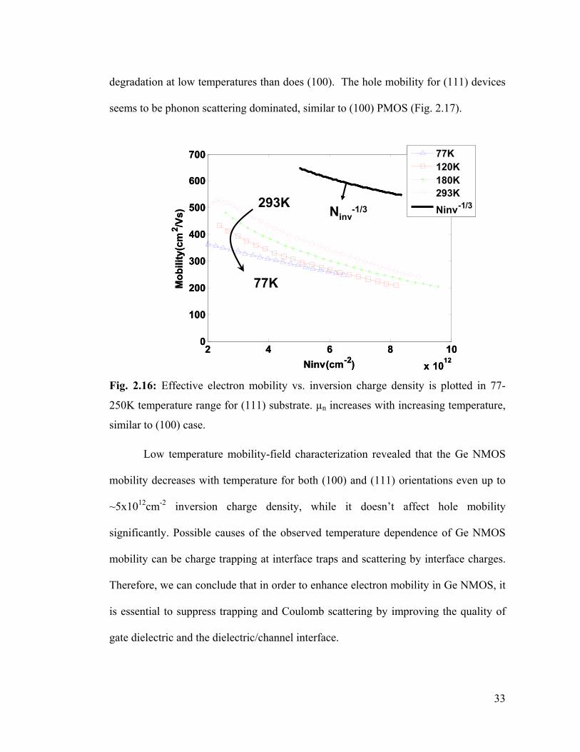
33
degradation at low temperatures than does (100). The hole mobility for (111) devices
seems to be phonon scattering dominated, similar to (100) PMOS (Fig. 2.17).
Fig. 2.16: Effective electron mobility vs. inversion charge density is plotted in 77-
250K temperature range for (111) substrate. µn increases with increasing temperature,
similar to (100) case.
Low temperature mobility-field characterization revealed that the Ge NMOS
mobility decreases with temperature for both (100) and (111) orientations even up to
~5x1012cm-2 inversion charge density, while it doesn’t affect hole mobility
significantly. Possible causes of the observed temperature dependence of Ge NMOS
mobility can be charge trapping at interface traps and scattering by interface charges.
Therefore, we can conclude that in order to enhance electron mobility in Ge NMOS, it
is essential to suppress trapping and Coulomb scattering by improving the quality of
gate dielectric and the dielectric/channel interface.
2 4 6 8 10x 10
12
0
100
200
300
400
500
600
700
Ninv(cm-2)
Mob
ility
(cm
2 /Vs)
77K120K180K293KNinv-1/3293K
77K
Ninv-1/3
2 4 6 8 10x 10
12
0
100
200
300
400
500
600
700
Ninv(cm-2)
Mob
ility
(cm
2 /Vs)
77K120K180K293KNinv-1/3293K
77K
Ninv-1/3
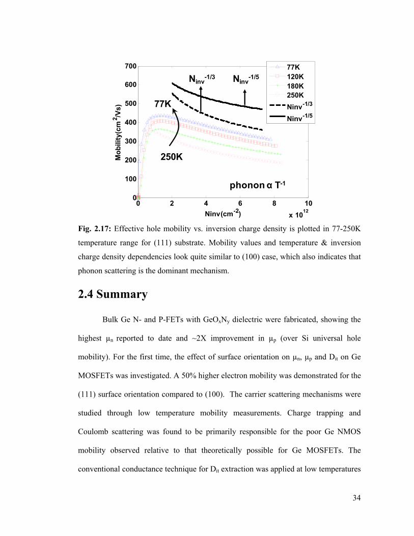
34
Fig. 2.17: Effective hole mobility vs. inversion charge density is plotted in 77-250K
temperature range for (111) substrate. Mobility values and temperature & inversion
charge density dependencies look quite similar to (100) case, which also indicates that
phonon scattering is the dominant mechanism.
2.4 Summary
Bulk Ge N- and P-FETs with GeOxNy dielectric were fabricated, showing the
highest µn reported to date and ~2X improvement in µp (over Si universal hole
mobility). For the first time, the effect of surface orientation on µn, µp and Dit on Ge
MOSFETs was investigated. A 50% higher electron mobility was demonstrated for the
(111) surface orientation compared to (100). The carrier scattering mechanisms were
studied through low temperature mobility measurements. Charge trapping and
Coulomb scattering was found to be primarily responsible for the poor Ge NMOS
mobility observed relative to that theoretically possible for Ge MOSFETs. The
conventional conductance technique for Dit extraction was applied at low temperatures
0 2 4 6 8 10x 1012
0
100
200
300
400
500
600
700
Ninv(cm-2)
Mob
ility
(cm
2 /Vs)
77K120K180K250KNinv-1/3
Ninv-1/5
250K
77K
Ninv-1/3 Ninv
-1/5
phonon α T-1
35
to map out the Dit distribution across the Ge bandgap and in the proximity of the band
edges. Higher trap densities near the conduction band edge of (100) Ge was observed,
whereas, the (111) substrate exhibited a more symmetric Dit distribution. These
findings are potentially important for better understanding of Ge-based transistors for
future CMOS applications.
2.5 References [1] K. Saraswat, C. O. Chui, K. Donghyun, T. Krishnamohan, A. Pethe, “High
mobility materials and novel device structures for high performance
nanoscaleMOSFETs”, IEDM Tech. Dig., pp.659-662, 2006.
[2] E. P. Gusev, H. Shang, M. Copel, M. Grilbeyuk, C. D’Emic, P. Kozlowski, T.
Zabel, “Microstructure and thermal stability of HfO2 gate dielectric deposited on
Ge(100)”, App. Phys. Lett., vol. 85, pp. 2334-2337, 2004.
[3] C. O. Chui, S. Ramanathan, B. B. Triplet, P. C. McIntyre, K. C. Saraswat,
“Germanium MOS capacitors incorporating ultrathin High-K gate dielectric”,
IEEE Elec. Dev. Lett., vol.23, pp. 473-476, 2002.
[4] S. Iwauchi, T. Tanaka, “Interface properties of Al2O3-Ge structure and
characteristics of Al2O3-Ge MOS transistors”, Jpn. J. Appl. Phys., vol.10, pp. 260-
265, 1971.
[5] D. S. Yu, K. C. Chiang, C. F. Cheng, A. Chin, C. Zhu, M. F. Li, D-L. Kwong,
“Fully silicided NiSi:Hf-LaAlO3/SC-GOI n-MOSFETs with high electron
mobility”, IEEE Elec. Dev. Lett., vol.25, pp. 559-562, 2004.
[6] H. L. Shang, H. Okorn-Schmidt, K. K. Chan, M. Copel, J. A. Ott, P. M.
Kozlowski, S. E. Steen, S. A. Cordes, H.-S. P. Wong, E. C. Jones,and W. E.
36
Haensch, “High mobility p-Channel germanium MOSFETswith a thin
Geoxynitride gate dielectric”, IEDM Tech. Dig., pp.441–444, 2002.
[7] H. Shang, K-L. Lee, P. Kozlowski, C. D’emic, I. Babich, E. Sikorski, M. Ieong,
H.-S. P. Wong, K. Guarini, W. Haensch, “Self-aligned n-channel germanium
MOSFETs with a thin Geoxynitride gate dielectric and tungsten gate”, IEEE Elec.
Dev. Lett., vol.25, pp. 135-138, 2004.
[8] S. J. Whang, S. J. Lee, F. Gao, N. Wu, C. X. Zhu, J. S. Pan, L. J. Tang, D. L.
Kwong, “Germanium p- & n-MOSFETs fabricated with novel surface passivation
(plasma-PH/sub 3/ and thin AlN) and TaN/HfO/sub 2/ gate stack”, IEDM Tech.
Dig., pp. 307-310, 2004.
[9] D. Kuzum, A. J. Pethe, T. Krishnamohan, Y. Oshima, Y. Sun, J. P. McVittie, P. A.
Pianetta, P. C. McIntyre, and K.C. Saraswat, “Interface-Engineered Ge (100) and
(111) , N- and P-FETs with High Mobility”, IEDM Tech. Dig., pp. 723-726, 2007.
[10] T. Deegan and G. Hughes, “An X-ray photoelectron spectroscopy study of the
HF etching of native oxides on Ge (111) and Ge (100) surfaces”, Appl. Surf. Sci.,
vol. 123–124, pp. 66–70, 1998.
[11] A. Delabie, F. Bellenger, M. Houssa, T. Conard, S. V. Elshocht, M. Caymax,
M. Heyns, M. Meuris, “Effective electrical passivation of Ge (100) for high-K gate
dielectric layers using germanium oxide”, App. Phys. Lett., vol. 91, pp. 082904,
2007..
[12] Y. Fukuda, T. Ueno, S. Hirono, S. Hashimoto, “Electrical characterization of
Ge-oxide/Ge interface prepared by electron-cyclotron-resonance plasma
irradiation”, Jpn. J. Appl. Phys., vol. 44, pp. 6981-6984, 2005.
37
[13] D. Kuzum, T. Krishnamohan, A. J. Pethe , Ali K. Okyay, Y. Oshima, Y. Sun,
J. P. McVittie, P. A. Pianetta, P. C. McIntyre, and K.C. Saraswat, “Ge Interface
Engineering with Ozone Oxidation for Low Interface State Density”, IEEE Elec.
Dev. Lett., vol.29, pp. 328-330, 2008.
[14] D. J. Hymes, J. J. Rosenberg, “Growth and materials characterization of native
germanium nitride thin films on germanium”, J. Electrochem.Soc., vol. 135, pp.
961-965, 1988.
[15] S. Takagi, T. Maeda, N. Takoa, M. Nishizawa, Y. Morita, K. Ikeda, Y.
Yamashita, M. Nishikawa, H. Kumagai, R. Nakane, S. Sugahara, N. Sugiyama,
“Gate dielectric formation and MIS interface characterization on Ge”,
Microelectronic Engineering, vol. 24, pp. 2314-2319, 2007.
[16] K. Martens, C. O. Chui, G. Brammertz,B. De Jaeger,D. Kuzum,M. Meuris, M.
Heyns, T. Krishnamohan,K. Saraswat, H. E. Maes, G. Groeseneken, “On the
Correct Extraction of Interface Trap Density of MOS Devices With High-Mobility
Semiconductor Substrates”, IEEE Trans. Elec. Dev., vol.55, pp.547-556, 2008.
[17] J. D. Wiley, “Mobility of holes in in III-V compounds”, in Semiconductors and
Semimetals. Vol. 10, ed. by R. K. Willardson, A. C. Beer, Academic Press, New
York, 1975.
[18] C. T.Sah, T. H. Ning, L. L. Tschopp, “ Scattering of electrons by surface oxide
charges and by lattice vibrations at the silicon-silicon dioxide interface”, Surf Sci.,
vol.32, pp. 561-575, 1972.
38
[19] T. H. Ning, C. T. Sah, “Theory of scattering of electrons in a nondegenerate-
semiconductor-surface inversion layer by surface oxide charges”, Phys. Rev. B,
vol. 6, pp. 4605-4613, 1972.
[20] D. S. Jeon, D. E. Burk, “MOSFET inversion layer mobilities- a physically
based semi-empirical model for a wide temperature range”, IEEE Trans.Elec.
Dev., vol.36, pp.1456-1463, 1989.
[21] S. Takagi, A. Toriumi, M. Iwase, H. Tango, “On the universality of inversion
layer inversion layer mobility in Si MOSFET’s: Part I- effects of substrate
impurity concentration”, IEEE Trans. Elec. Dev., vol.41, pp. 2357-2362, 1994.
[22] A. Pethe, T. Krishnamohan, K. Uchida, K. C. Saraswat, “Analytical modeling
of Ge and Si double-gate (DG) N-FETs and the effect of process induced
variations (PIV) on device performance”, SISPAD, pp. 359-362, 2004.
[23] Y.-J. Yang, W. S. Ho, C.–F. Huang, S. T. Chang, C. W. Liu, “Electron
mobility enhancement in strained-germanium n-channel metal-oxide-
semiconductor field-effect transistors”, Appl. Phys. Lett., vol. 91, pp. 102103,
2007.

39
40
Chapter 3 Interface Characterization Techniques For Ge
3.1 Introduction Capacitance and conductance based techniques are extensively used in Si
CMOS technology to characterize parameters of Si MOSFETs and MOS capacitors
such as the flat-band voltage, effective oxide thickness, work function, fixed charge,
doping level and density of interface traps. Among those, interface trap density (Dit) is
very critical to quantify the electrical quality of semiconductor/dielectric (channel/gate
dielectric) interface.
Surface passivation of Ge is a key challenge to obtain excellent gate
channel/dielectric interface and to achieve high performance Ge MOSFETs. Many
attempts have been made to engineer Ge interface including ozone oxidation [1],
thermal oxidation [2], fluorine treatment [3], Si passivation [4], [5], sulfur passivation
[6] and nitridation [7], [8]. Accurate characterization of gate dielectric/channel
interface is crucial for relative comparison of different passivation techniques.
41
Besides, a deeper understanding of surface passivation is needed to address interface
related-performance problems, especially for NMOS transistors [9], [10]. However,
the conventional Dit extraction techniques cannot be directly applied to Ge. The low
bandgap of Ge makes the electrical interface characterization a big challenge. In this
chapter, a brief review of interface characterization techniques in literature is given.
Then, the low temperature conductance technique to extract Dit distribution at
Ge/dielectric interfaces is illustrated. The low temperature conductance measurements
discussed in this chapter, are based on Nicollian-Goetzberger (N-G) method, which is
also known as the conductance technique for Dit extraction [11].
3.2 Overview of Interface Characterization Techniques
3.2.1 Low Frequency (Quasi-static) Methods The low frequency or quasi-static method is a common interface trap density
measurement method. It provides information only on the interface trap density but
not on their capture cross sections or time constants. The effect of interface traps on
high and low frequency capacitance curves are explained in Fig 3.1 [12]. In the case of
high frequency capacitance measurements, the interface traps cannot follow the ac
probe frequency. However, they can follow dc gate voltage sweep speed. Therefore,
interface traps are filled with carriers as gate voltage is swept from accumulation to
inversion. Therefore, the charging of interface traps causes a stretch-out in the high
frequency capacitance curves. The stretch-out in case of high frequency measurements
is not a result of interface trap capacitance, but rather an effect of filling interface traps
as gate voltage is swept. Interface traps respond to probe-frequency at low
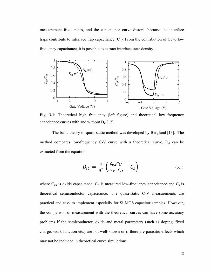
42
measurement frequencies, and the capacitance curve distorts because the interface
traps contribute to interface trap capacitance (Cit). From the contribution of Cit to low
frequency capacitance, it is possible to extract interface state density.
Fig. 3.1: Theoretical high frequency (left figure) and theoretical low frequency
capacitance curves with and without Dit [12].
The basic theory of quasi-static method was developed by Berglund [13]. The
method compares low-frequency C-V curve with a theoretical curve. Dit can be
extracted from the equation:
(3.1)
where Cox is oxide capacitance, Clf is measured low-frequency capacitance and Cs is
theoretical semiconductor capacitance. The quasi-static C-V measurements are
practical and easy to implement especially for Si MOS capacitor samples. However,
the comparison of measurement with the theoretical curves can have some accuracy
problems if the semiconductor, oxide and metal parameters (such as doping, fixed
charge, work function etc.) are not well-known or if there are parasitic effects which
may not be included in theoretical curve simulations.
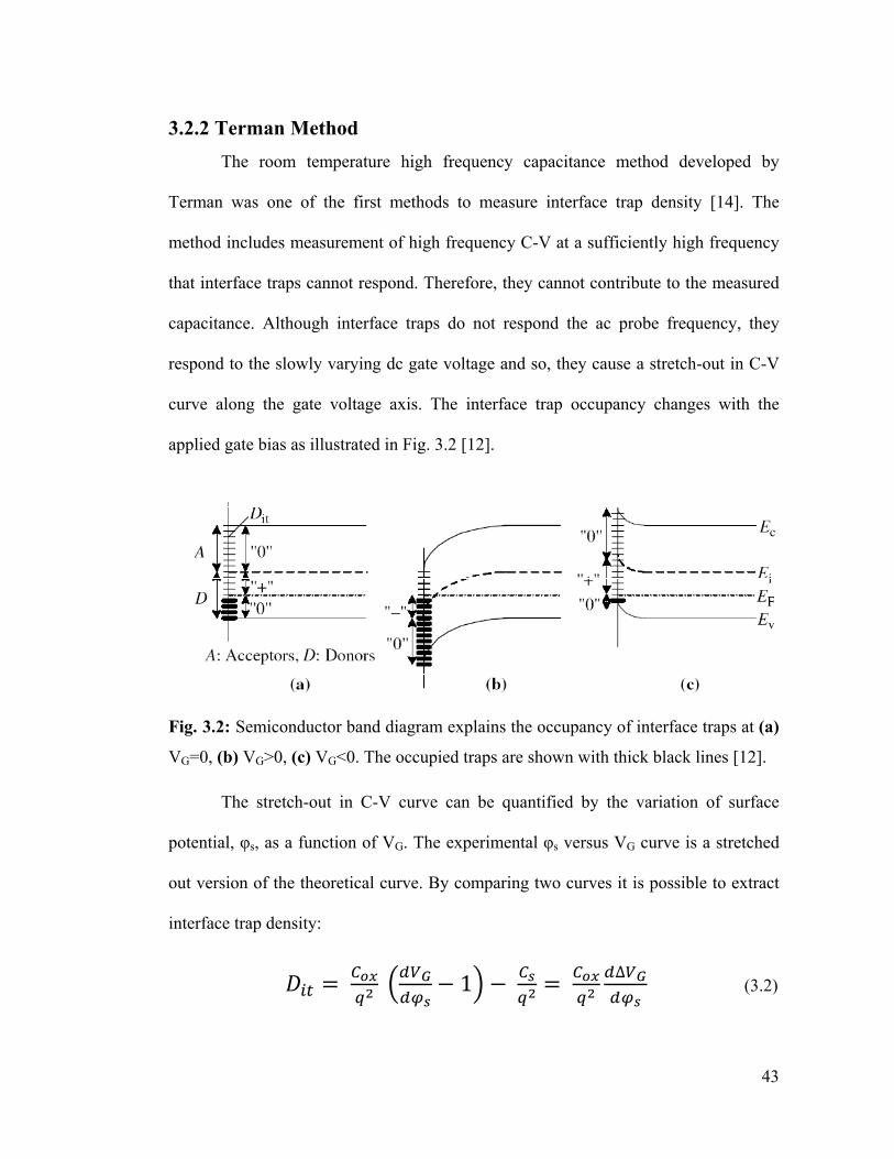
43
3.2.2 Terman Method The room temperature high frequency capacitance method developed by
Terman was one of the first methods to measure interface trap density [14]. The
method includes measurement of high frequency C-V at a sufficiently high frequency
that interface traps cannot respond. Therefore, they cannot contribute to the measured
capacitance. Although interface traps do not respond the ac probe frequency, they
respond to the slowly varying dc gate voltage and so, they cause a stretch-out in C-V
curve along the gate voltage axis. The interface trap occupancy changes with the
applied gate bias as illustrated in Fig. 3.2 [12].
Fig. 3.2: Semiconductor band diagram explains the occupancy of interface traps at (a)
VG=0, (b) VG>0, (c) VG<0. The occupied traps are shown with thick black lines [12].
The stretch-out in C-V curve can be quantified by the variation of surface
potential, φs, as a function of VG. The experimental φs versus VG curve is a stretched
out version of the theoretical curve. By comparing two curves it is possible to extract
interface trap density:
1 ∆ (3.2)
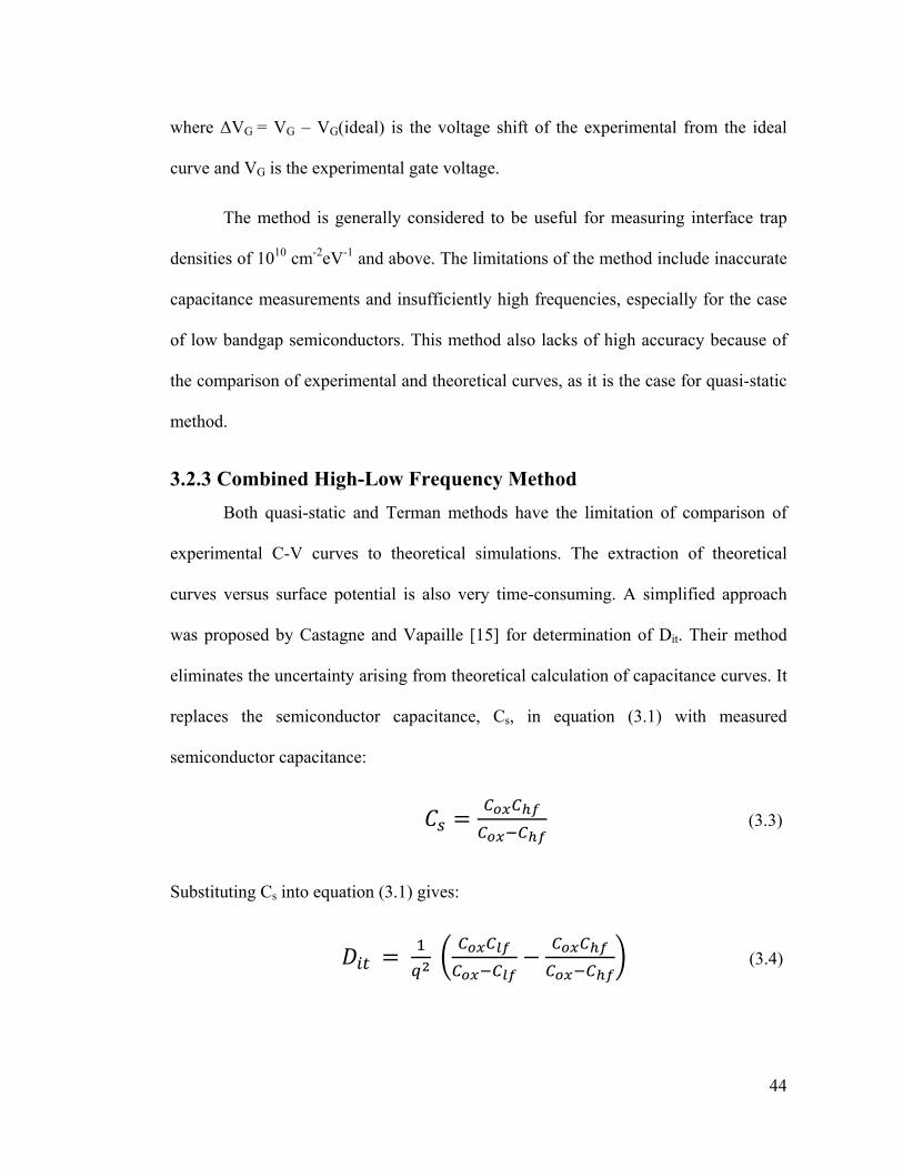
44
where ΔVG = VG – VG(ideal) is the voltage shift of the experimental from the ideal
curve and VG is the experimental gate voltage.
The method is generally considered to be useful for measuring interface trap
densities of 1010 cm-2eV-1 and above. The limitations of the method include inaccurate
capacitance measurements and insufficiently high frequencies, especially for the case
of low bandgap semiconductors. This method also lacks of high accuracy because of
the comparison of experimental and theoretical curves, as it is the case for quasi-static
method.
3.2.3 Combined High-Low Frequency Method Both quasi-static and Terman methods have the limitation of comparison of
experimental C-V curves to theoretical simulations. The extraction of theoretical
curves versus surface potential is also very time-consuming. A simplified approach
was proposed by Castagne and Vapaille [15] for determination of Dit. Their method
eliminates the uncertainty arising from theoretical calculation of capacitance curves. It
replaces the semiconductor capacitance, Cs, in equation (3.1) with measured
semiconductor capacitance:
(3.3)
Substituting Cs into equation (3.1) gives:
(3.4)
45
Equation (3.4) enables the determination of Dit in a completely experimental
way. However, it is only valid in a limited range of the bandgap, from the onset
inversion to a surface potential towards majority carrier band edge where the ac
measurement frequency is equal to the inverse of interface trap time constant. The
higher the frequency the closer to the band edge we can probe. But, this equation is
not valid in inversion. A comparison of Chf and Clf curves is shown in Fig. 3.3.
Fig. 3.3: High and low frequency capacitance-gate voltage curves are shown. The
ΔC/Cox offset is due to interface traps [12].
This Dit measurement method is widely used for Si. However it is not directly
applicable to low-bandgap semiconductors, such as Ge. Obtaining an accurate high
frequency capacitance curve, which does not include any contribution from interface
trap capacitance, is very difficult for Ge due to the low bandgap. The interface trap
time constants are so short that most of them cannot be measured even at 1 MHz. Also
thermal generation colors the capacitance measurements and causes inversion
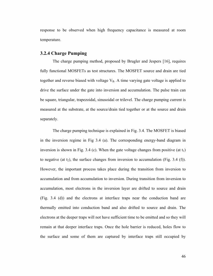
46
response to be observed when high frequency capacitance is measured at room
temperature.
3.2.4 Charge Pumping The charge pumping method, proposed by Brugler and Jespers [16], requires
fully functional MOSFETs as test structures. The MOSFET source and drain are tied
together and reverse biased with voltage VR. A time varying gate voltage is applied to
drive the surface under the gate into inversion and accumulation. The pulse train can
be square, triangular, trapezoidal, sinusoidal or trilevel. The charge pumping current is
measured at the substrate, at the source/drain tied together or at the source and drain
separately.
The charge pumping technique is explained in Fig. 3.4. The MOSFET is biased
in the inversion regime in Fig 3.4 (a). The corresponding energy-band diagram in
inversion is shown in Fig. 3.4 (c). When the gate voltage changes from positive (at t1)
to negative (at t2), the surface changes from inversion to accumulation (Fig. 3.4 (f)).
However, the important process takes place during the transition from inversion to
accumulation and from accumulation to inversion. During transition from inversion to
accumulation, most electrons in the inversion layer are drifted to source and drain
(Fig. 3.4 (d)) and the electrons at interface traps near the conduction band are
thermally emitted into conduction band and also drifted to source and drain. The
electrons at the deeper traps will not have sufficient time to be emitted and so they will
remain at that deeper interface traps. Once the hole barrier is reduced, holes flow to
the surface and some of them are captured by interface traps still occupied by
47
electrons (Fig. 3.4 (e)). The recombination of holes with trapped electrons results in a
net charge pumping current, which is proportional to Dit.
Fig. 3.4: Device cross-sections and energy band diagrams for charge pumping
measurements [12].
Charge pumping is one of the most reliable and sensitive techniques for Dit
characterization. However, when it is applied on Ge at room temperature, only a very
small part of the Ge bandgap, close to midgap region, can be scanned. The interface
trap density can be underestimated because the traps near the bandedges are not
measured. Besides, charge pumping technique requires a fully functional Ge
MOSFET, which may not be very practical to characterize a large number of samples.
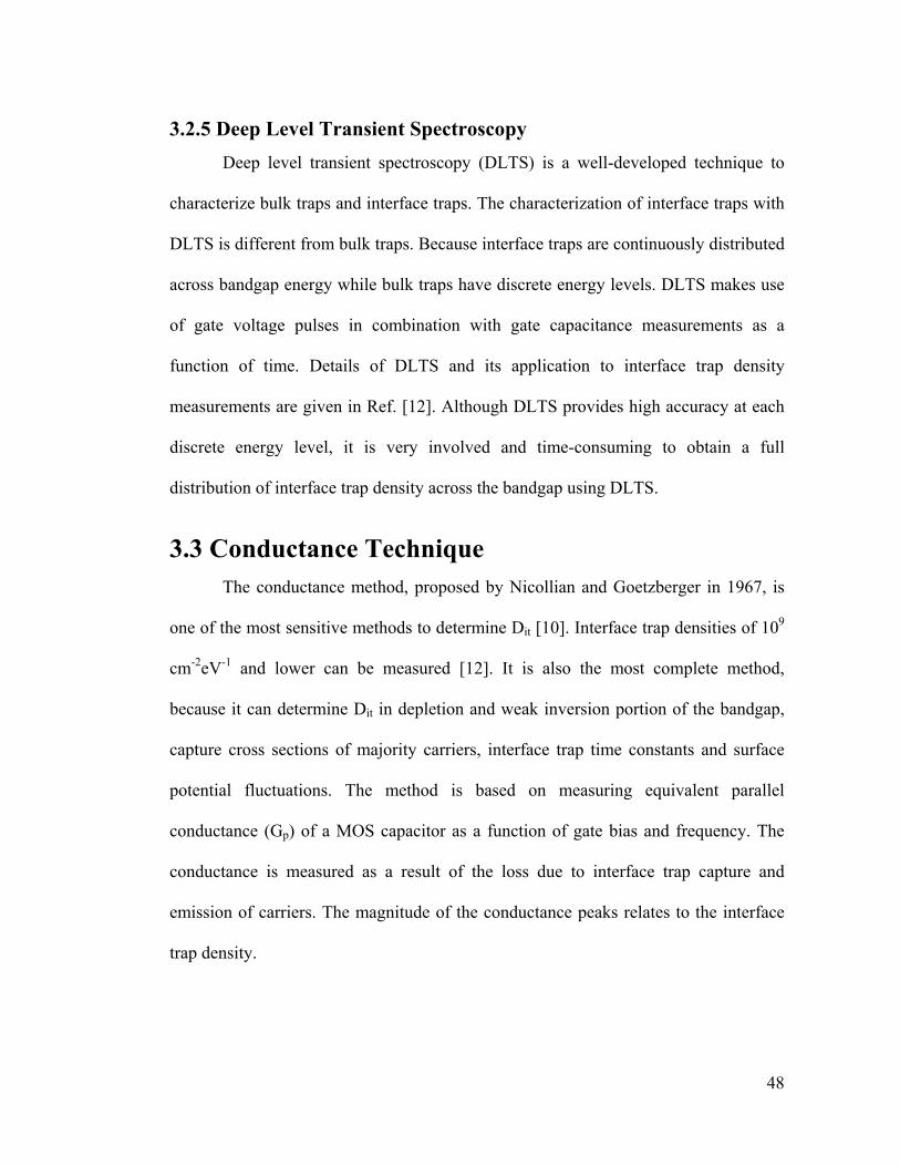
48
3.2.5 Deep Level Transient Spectroscopy Deep level transient spectroscopy (DLTS) is a well-developed technique to
characterize bulk traps and interface traps. The characterization of interface traps with
DLTS is different from bulk traps. Because interface traps are continuously distributed
across bandgap energy while bulk traps have discrete energy levels. DLTS makes use
of gate voltage pulses in combination with gate capacitance measurements as a
function of time. Details of DLTS and its application to interface trap density
measurements are given in Ref. [12]. Although DLTS provides high accuracy at each
discrete energy level, it is very involved and time-consuming to obtain a full
distribution of interface trap density across the bandgap using DLTS.
3.3 Conductance Technique The conductance method, proposed by Nicollian and Goetzberger in 1967, is
one of the most sensitive methods to determine Dit [10]. Interface trap densities of 109
cm-2eV-1 and lower can be measured [12]. It is also the most complete method,
because it can determine Dit in depletion and weak inversion portion of the bandgap,
capture cross sections of majority carriers, interface trap time constants and surface
potential fluctuations. The method is based on measuring equivalent parallel
conductance (Gp) of a MOS capacitor as a function of gate bias and frequency. The
conductance is measured as a result of the loss due to interface trap capture and
emission of carriers. The magnitude of the conductance peaks relates to the interface
trap density.
49
The equivalent circuit for a MOS capacitor is shown in Fig. 3.5 (a). It consists
of oxide capacitance (Cox), semiconductor capacitance (Cs), and interface trap
capacitance (Cit). The lossy capture-emission process of carriers is modeled as a
resistor (Rit) in series with Cit. The circuit can be simplified as in Fig. 3.5 (b), where
Cp and Gp are given as:
, (3.5)
where Cit= q2Dit, ω=2πf, f is measurement frequency and Tit is the interface trap time
constant.
Fig. 3.5: Equivalent circuit models for conductance measurements; (a) MOS capacitor
with interface traps, (b) simplified circuit of (a), (c) measured circuit, (d) including
series resistance and tunnel conductance due to gate leakage [12].
In Fig. 3.5 (c), the measured circuit diagram is shown. Cp and Gp can be
extracted from measured values of Cm and Gm, once Cox is known. Parasitic series
resistance arising from low substrate doping or contact resistances or leakage through
gate dielectric, can contribute measured admittance. They need to be included in the
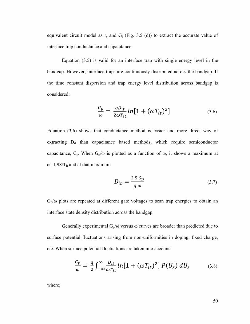
50
equivalent circuit model as rs and Gt (Fig. 3.5 (d)) to extract the accurate value of
interface trap conductance and capacitance.
Equation (3.5) is valid for an interface trap with single energy level in the
bandgap. However, interface traps are continuously distributed across the bandgap. If
the time constant dispersion and trap energy level distribution across bandgap is
considered:
1 (3.6)
Equation (3.6) shows that conductance method is easier and more direct way of
extracting Dit than capacitance based methods, which require semiconductor
capacitance, Cs. When Gp/ω is plotted as a function of ω, it shows a maximum at
ω=1.98/Tit and at that maximum
.
(3.7)
Gp/ω plots are repeated at different gate voltages to scan trap energies to obtain an
interface state density distribution across the bandgap.
Generally experimental Gp/ω versus ω curves are broader than predicted due to
surface potential fluctuations arising from non-uniformities in doping, fixed charge,
etc. When surface potential fluctuations are taken into account:
1 (3.8)
where;
51
√
(3.9)
P(Us) is the probability distribution of surface potential fluctuation, U is the
normalized mean surface potential and σ is the standard deviation.
Conductance technique, developed by Nicollian and Goetzberger, has been
intensively studied on semiconductor insulator interfaces. All the details of
conductance technique is well-documented [10]. Conductance technique has several
advantages over other interface characterization techniques: 1) Sensitivity, 2)
Simplicity and easy implementation, 3) It can measure both low and high levels of Dit,
4) It doesn’t require MOSFETs, a simple MOS capacitor is sufficient. When
conductance technique is used at room temperature, it is valid in the depletion regime
and it requires multi-frequency capacitance (C-V) and conductance (G-V)
measurements. However, in case of low bandgap semiconductors, low temperature
measurements are needed to suppress the thermal generation affecting C-V and G-V
measurements. Application of conductance technique on low bandgap
semiconductors, specifically on Ge, will be discussed in the next sections.
3.4 Ge: A low bandgap semiconductor The conductance method is a reliable way to extract Dit. However, for low
bandgap materials such as Ge, time constants for capture and emission processes of
carriers through interface traps are much shorter than for Si, due to their smaller
bandgap. At room temperature, conductance does not show the interface trap behavior
typical of Si MOS devices due to thermal generation and weak inversion response in
52
the low bandgap Ge. The complete inversion capacitance measured at room
temperature is attributed to thermal generation while the humps observed in C-V
measurements in the depletion or the on-set inversion regions are attributed the weak
inversion response. The humps due to weak inversion response and their behavior with
temperature and frequency is studied for Ge in detail [11]. In addition to weak
inversion humps, the inversion response due to the thermal generation of inversion
carriers is also shown in Fig. 3.6.
Fig. 3.6: Temperature and frequency dependence of n-type Ge/GeON MOS
capacitance. Weak inversion response and complete inversion due to thermal
generation are shown [11].
For measurements done at temperatures ~250 K or above, conductance peaks
are observed corresponding to weak inversion bias region. Weak inversion response is
a result of interaction of interface traps with both majority and minority carrier bands
[11]. The interaction with both bands is more prominent especially for the interface
traps around the midgap region (Fig. 3.7 (a)). In the weak inversion regime at
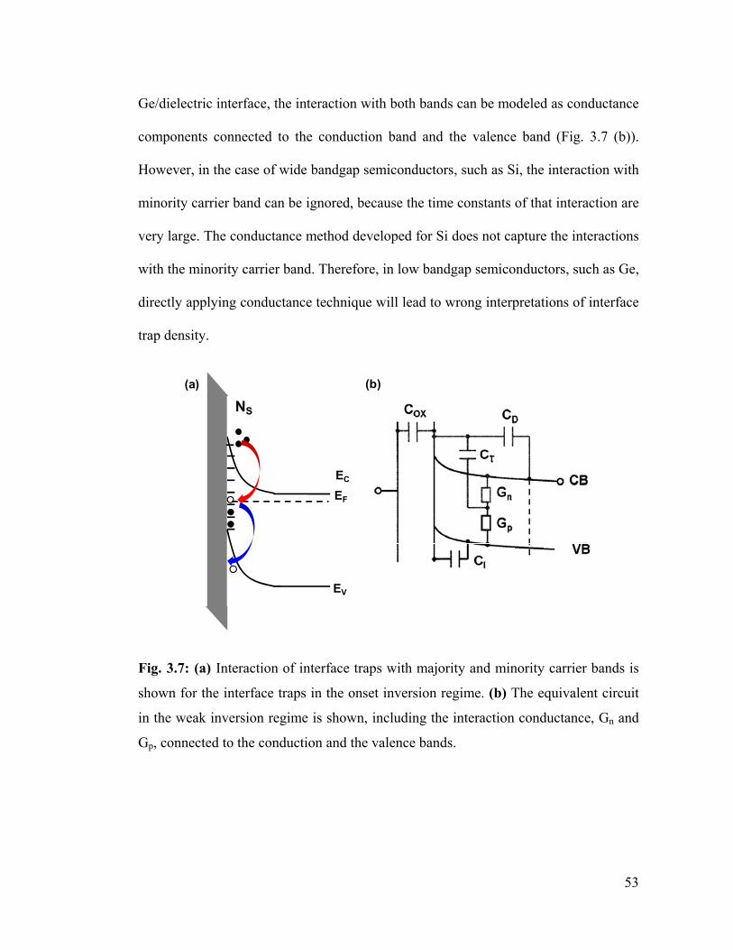
53
Ge/dielectric interface, the interaction with both bands can be modeled as conductance
components connected to the conduction band and the valence band (Fig. 3.7 (b)).
However, in the case of wide bandgap semiconductors, such as Si, the interaction with
minority carrier band can be ignored, because the time constants of that interaction are
very large. The conductance method developed for Si does not capture the interactions
with the minority carrier band. Therefore, in low bandgap semiconductors, such as Ge,
directly applying conductance technique will lead to wrong interpretations of interface
trap density.
Fig. 3.7: (a) Interaction of interface traps with majority and minority carrier bands is
shown for the interface traps in the onset inversion regime. (b) The equivalent circuit
in the weak inversion regime is shown, including the interaction conductance, Gn and
Gp, connected to the conduction and the valence bands.
EC
EV
NS
EF
(a) (b)
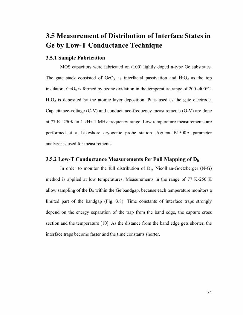
54
3.5 Measurement of Distribution of Interface States in Ge by Low-T Conductance Technique
3.5.1 Sample Fabrication MOS capacitors were fabricated on (100) lightly doped n-type Ge substrates.
The gate stack consisted of GeOx as interfacial passivation and HfO2 as the top
insulator. GeOx is formed by ozone oxidation in the temperature range of 200 -400ºC.
HfO2 is deposited by the atomic layer deposition. Pt is used as the gate electrode.
Capacitance-voltage (C-V) and conductance-frequency measurements (G-V) are done
at 77 K- 250K in 1 kHz-1 MHz frequency range. Low temperature measurements are
performed at a Lakeshore cryogenic probe station. Agilent B1500A parameter
analyzer is used for measurements.
3.5.2 Low-T Conductance Measurements for Full Mapping of Dit
In order to monitor the full distribution of Dit, Nicollian-Goetzberger (N-G)
method is applied at low temperatures. Measurements in the range of 77 K-250 K
allow sampling of the Dit within the Ge bandgap, because each temperature monitors a
limited part of the bandgap (Fig. 3.8). Time constants of interface traps strongly
depend on the energy separation of the trap from the band edge, the capture cross
section and the temperature [10]. As the distance from the band edge gets shorter, the
interface traps become faster and the time constants shorter.
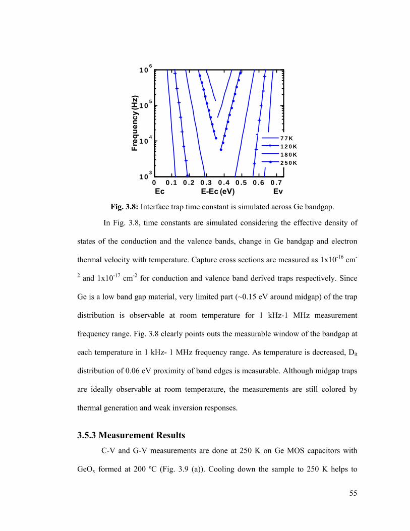
55
Fig. 3.8: Interface trap time constant is simulated across Ge bandgap.
In Fig. 3.8, time constants are simulated considering the effective density of
states of the conduction and the valence bands, change in Ge bandgap and electron
thermal velocity with temperature. Capture cross sections are measured as 1x10-16 cm-
2 and 1x10-17 cm-2 for conduction and valence band derived traps respectively. Since
Ge is a low band gap material, very limited part (~0.15 eV around midgap) of the trap
distribution is observable at room temperature for 1 kHz-1 MHz measurement
frequency range. Fig. 3.8 clearly points outs the measurable window of the bandgap at
each temperature in 1 kHz- 1 MHz frequency range. As temperature is decreased, Dit
distribution of 0.06 eV proximity of band edges is measurable. Although midgap traps
are ideally observable at room temperature, the measurements are still colored by
thermal generation and weak inversion responses.
3.5.3 Measurement Results C-V and G-V measurements are done at 250 K on Ge MOS capacitors with
GeOx formed at 200 ºC (Fig. 3.9 (a)). Cooling down the sample to 250 K helps to
0 0.1 0.2 0.3 0.4 0.5 0.6 0.710
3
104
105
106
77K120K180K250K
Freq
uenc
y (H
z)
E-Ec (eV) EvEc
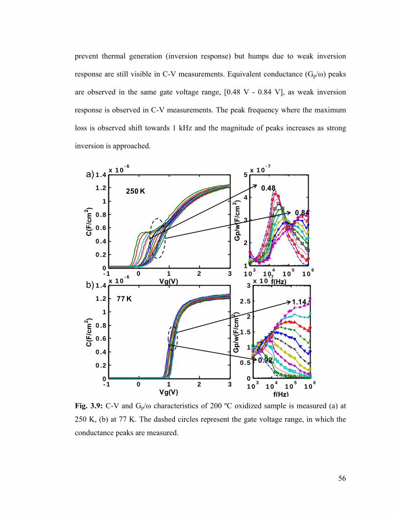
56
prevent thermal generation (inversion response) but humps due to weak inversion
response are still visible in C-V measurements. Equivalent conductance (Gp/ω) peaks
are observed in the same gate voltage range, [0.48 V - 0.84 V], as weak inversion
response is observed in C-V measurements. The peak frequency where the maximum
loss is observed shift towards 1 kHz and the magnitude of peaks increases as strong
inversion is approached.
Fig. 3.9: C-V and Gp/ω characteristics of 200 ºC oxidized sample is measured (a) at
250 K, (b) at 77 K. The dashed circles represent the gate voltage range, in which the
conductance peaks are measured.
103
104
105
106
0
0.5
1
1.5
2
2.5
3x 10
-7
f(Hz)
Gp/
w(F
/cm
2 )
-1 0 1 2 30
0.2
0.4
0.6
0.8
1
1.2
1.4x 10
-6
Vg(V)
C(F
/cm
2 )
103
104
105
106
1
2
3
4
5x 10
-7
f(Hz)
Gp/
w(F
/cm
2 )
0.84
0.48250 K
-1 0 1 2 30
0.2
0.4
0.6
0.8
1
1.2
1.4x 10
-6
Vg(V)
C(F
/cm
2 )
1.14
0.92
77 K
a)
b)
57
Cooling down the sample to 77 K, the effect of weak inversion response on C-
V and G-V completely disappears (Fig. 3.9 (b)). C-V curves look steeper in spite of
the frequency dependent flat-band shift in the depletion region. At 77 K, Gp/ω respond
at higher frequencies as gate bias is swept towards accumulation, [0.92 V – 1.14 V], as
faster traps closer to conduction band edge are probed.
Fig. 3.10: C-V and Gp/ω characteristics of the 400 ºC oxidized sample is measured (a)
at 250 K, (b) at 77 K.
The frequency dependent flat-band voltage shift is a characteristic of high
density of interface traps responding in the depletion part of the C-V curves. The
sample in Fig. 3.9 is intentionally chosen with higher Dit to show its effect on C-V and
-1.5 -1 -0.5 0 0.5 1 1.50
1
2
3
4
5x 10
-7
Vg(V)
C(F
/cm
2 )
103
104
105
0
0.5
1
1.5
2
2.5x 10
-7
f(Hz)
Gp/
w(F
/cm
2 )
-0.52
-0.28
250 K
-1.5 -1 -0.5 0 0.5 1 1.50
1
2
3
4x 10
-7
Vg(V)
C(F
/cm
2 )
103
104
105
106
0
0.5
1
1.5
2
2.5x 10
-8
f(Hz)
Gp/
w(F
/cm
2 ) 0.4
0.5277 K
a)
b)
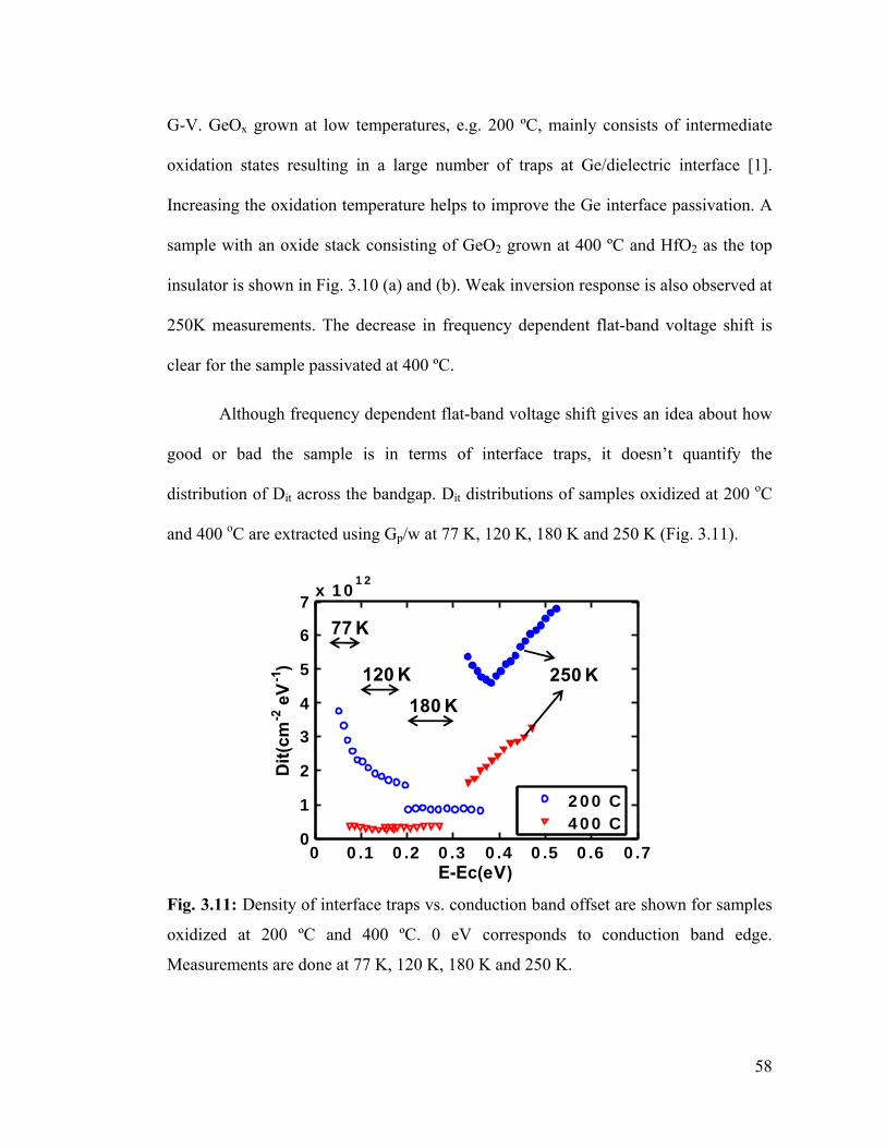
58
G-V. GeOx grown at low temperatures, e.g. 200 ºC, mainly consists of intermediate
oxidation states resulting in a large number of traps at Ge/dielectric interface [1].
Increasing the oxidation temperature helps to improve the Ge interface passivation. A
sample with an oxide stack consisting of GeO2 grown at 400 ºC and HfO2 as the top
insulator is shown in Fig. 3.10 (a) and (b). Weak inversion response is also observed at
250K measurements. The decrease in frequency dependent flat-band voltage shift is
clear for the sample passivated at 400 ºC.
Although frequency dependent flat-band voltage shift gives an idea about how
good or bad the sample is in terms of interface traps, it doesn’t quantify the
distribution of Dit across the bandgap. Dit distributions of samples oxidized at 200 oC
and 400 oC are extracted using Gp/w at 77 K, 120 K, 180 K and 250 K (Fig. 3.11).
Fig. 3.11: Density of interface traps vs. conduction band offset are shown for samples
oxidized at 200 ºC and 400 ºC. 0 eV corresponds to conduction band edge.
Measurements are done at 77 K, 120 K, 180 K and 250 K.
0 0.1 0.2 0.3 0.4 0.5 0.6 0.70
1
2
3
4
5
6
7x 10
12
E-Ec(eV)
Dit(
cm-2
eV
-1)
200 C400 C
250 K
77 K
120 K180 K
59
Minimum Dit at midgap for the sample oxidized at 400 oC is measured as
~3x1011cm-2eV-1. The sample grown at 200 oC shows a minimum Dit of 1x1012cm-2eV-
1 at midgap and Dit increases to 5x1012cm-2eV-1 close to band edges. Dit distribution of
two samples gives a quantitative comparison of interface trap densities which is
consistent with the frequency dependent flat-band shifts observed in the C-V
measurements (Fig. 3.9 and Fig. 3.10). It proves that low temperature conductance
measurements give an accurate relative comparison for samples with different
qualities of interface passivation in low bandgap semiconductors.
The effect of weak inversion response shows itself in Dit numbers extracted
using 250 K data. It results in over-estimation of Dit around the midgap and the weak
inversion regions. In general, the Dit extracted in weak inversion and inversion
regimes gives inaccurate numbers and distributions over the bandgap.
3.5.4 Effect of Series Resistance on Dit Measurements
Series resistance is very critical for accurate Dit measurements. Both
capacitance and conductance measurements can be affected by series resistance,
particularly at higher frequencies. Series resistance can originate from the bulk of
lightly doped substrates, contacts or probes. Special care should be exercised both in
preparation of samples and in techniques used during measurement. An important way
to avoid series resistance can be to measure small area capacitors or transistors.
Capacitors with area in the 10000 µm2 range generally have series resistance
problems. If series resistance effect is not very strong, the results can be corrected
[10], [12]. The conductance measurements are particularly sensitive to series
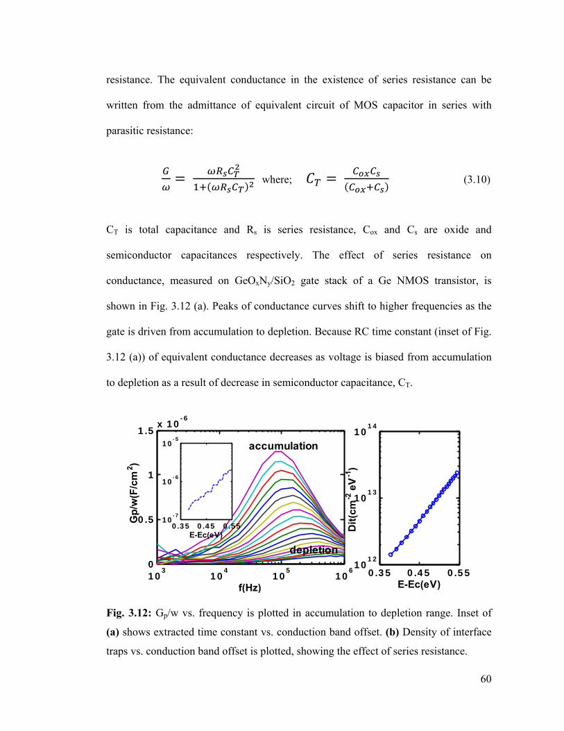
60
resistance. The equivalent conductance in the existence of series resistance can be
written from the admittance of equivalent circuit of MOS capacitor in series with
parasitic resistance:
where; (3.10)
CT is total capacitance and Rs is series resistance, Cox and Cs are oxide and
semiconductor capacitances respectively. The effect of series resistance on
conductance, measured on GeOxNy/SiO2 gate stack of a Ge NMOS transistor, is
shown in Fig. 3.12 (a). Peaks of conductance curves shift to higher frequencies as the
gate is driven from accumulation to depletion. Because RC time constant (inset of Fig.
3.12 (a)) of equivalent conductance decreases as voltage is biased from accumulation
to depletion as a result of decrease in semiconductor capacitance, CT.
Fig. 3.12: Gp/w vs. frequency is plotted in accumulation to depletion range. Inset of
(a) shows extracted time constant vs. conduction band offset. (b) Density of interface
traps vs. conduction band offset is plotted, showing the effect of series resistance.
103
104
105
106
0
0.5
1
1.5x 10
-6
f(Hz)
Gp/
w(F
/cm
2 )
0.35 0.45 0.5510
-7
10-6
10-5
E-Ec(eV)
accumulation
depletion
0.35 0.45 0.5510
12
1013
1014
E-Ec(eV)
Dit(
cm-2
eV
-1)
61
Although the peaks look quite similar to the conductance response of interface
traps, the voltage dependency of the peak shift and the time constant reveal that it is an
artifact of series resistance. In the case of interface trap response, the shift should be
towards lower frequencies under gate bias from accumulation to depletion. Treating
the peaks as interface trap response can cause misleading results in density of interface
traps. Dit extracted using series resistance related conductance peaks is shown in Fig.
3.12 (b). Linear trend of Dit can be an additional factor showing that conductance
peaks are not a consequence of interface trap response.
3.6 Summary
In summary, we discussed interface characterization techniques and interface
trap distribution measurements at Ge/dielectric interfaces in detail. Nicollian-
Goetzberger conductance technique was applied in the 77 K - 250 K temperature
range. It was demonstrated that low temperature conductance measurements give an
accurate relative comparison for samples with different qualities of interface
passivation. We showed that the temperature of 250 K is not sufficient to suppress the
effect of thermal generation and weak inversion responses in conductance
measurements. Measurable window of the bandgap at each temperature range was
calculated using interface trap time constants. The effect of series resistance on
conductance was clarified and the misleading Dit extractions were pointed.
62
3.7 References [1] D. Kuzum, T. Krishnamohan, A. J. Pethe, A. K. Okyay, Y. Oshima, Y. Sun, J. P.
Mcvittie, P. A. Pianetta, P. C. McIntyre, K. C. Saraswat, “Ge interface engineering
with ozone oxidation for low interface state density”, IEEE Elec. Dev. Lett., 29,
pp. 328-331, Apr. 2008.
[2] S. Takagi, T. Maeda, N. Taoka, M. Nishizawa, Y. Morita, K. Ikeda, Y. Yamashita,
M. Nishikawa, H. Kumagai, R. Nakane, S. Sugahara, N. Sugiyama, “Gate
dielectric formation and MIS interface characterization on Ge”, Microelectronic
Engineering, 84, pp. 2314-2319, Sep. 2007.
[3] R. L. Xie, T. H. Phung, W. He, M. B.Yu, C. X. Zhu, “Interface-engineered high-
mobility high-K/Ge p-MOSFETs with 1nm equivalent oxide thickness”, IEEE
Trans. Elec. Dev., 56, pp. 1330-1337, Jun. 2009.
[4] N. Taoka, M. Harada, Y. Yamashita, T. Yamamoto, N. Sugiyama, Shin-ichi
Takagi, “Effects of Si passivation on Ge metal-insulator-semiconductor interface
properties and inversion hole mobility”, Appl. Phys. Lett. 92, 113511, Mar. 2008.
[5] B. De Jaeger , R. Bonzom, F. Leys, O. Richard, J. Van Steenbergen, G.
Winderickx, E. Van Moorhem, G. Raskin, F. Letertre, T. Billon, M. Meuris and
M. Heyns, “Optimization of a thin layer epitaxial Si as Ge passivation layer to
demonstrate deep sub-micron n- and p-FETs on Ge-On-Insulator substrates”,
Microelectronic Engineering, 80, pp. 26-29, Jun. 2005.
[6] M. M. Frank, S. J. Koester, M. Copel, J. A. Ott, V. K. Paruchuri, H. Shang,
“Hafnium oxide gate dielectrics on sulfur-passivated germanium”, Appl. Phys.
Lett., 89, 112905, Sep. 2006.
63
[7] T. Maeda, M. Nishizawa, Y. Morita, “Role of germanium nitride interfacial layers
in HfO2/germanium nitride/germanium metal-insulator-semiconductor structures”,
Appl. Phys. Lett., 90, 072911, Feb. 2007.
[8] S. J. Whang, S. J. Lee, F. Fao, N. Wu, C. X. Zhu, J. S. Pan, L. J. Tang, D. L.
Kwong, “Germanium p- & n-MOSFETs fabricated with novel surface passivation
(plasma-PH3 and thin AlN) and TaN/ HfO2 gate stack”, IEDM Tech. Dig., pp. 307-
310, 2004.
[9] H. Shang, K-L. Lee, P. Kozlowski, C. D’emic, I. Babich, E. Sikorski, M. Ieong, H.
–S. P. Wong, K. Guarini, W. Haensch, “Self-aligned n-channel germanium
MOSFETs with a thin Ge oxynitride gate dielectric and tungsten gate”, IEEE Elec.
Dev. Lett., 25, pp. 135-138, Mar. 2004.
[10] E. H. Nicollian and J. R. Brews, MOS Physics and Technology, Wiley, New
York, 2003.
[11] K. Martens, C. O. Chui, G. Brammertz, B. De Jaeger, D. Kuzum, M. Meuris,
M. Heyns, T. Krishnamohan, K. Saraswat, H. E. Maes, G. Groeseneken, “On the
correct extraction of interface trap density of MOS devices with high-mobility
semiconductor substrates”, IEEE Trans. Elec. Dev.,55, pp. 547-555, Feb. 2008.
[12] D. K. Schroder, Semiconductor Material and Device Characterization, Wiley,
New York, 2006.
[13] C. N. Berglund, “Surface states at steam-grown silicon-silicon dioxide
interfaces”, IEEE Trans. Elec. Dev.,13, pp. 701-705, Oct. 1966.
64
[14] L. M. Terman, “An investigation of surface states at a Silicon/Silicon Oxide
interface employing metal-oxide-silicon diodes”, Solid-State Electronics, 31,1077-
1082, June 1988.
[15] R. Castagne and A. Vapaille, “Description of SiO2-Si interface properties by
means very low frequency MOS capacitance measurements”, Surf. Sci., 28, 157-
193, Nov. 1971
[16] J. S. Brugler and P. G. A. Jespers, “Charge pumping in MOS devices”, IEEE
Trans. Elec. Dev.,16, pp. 297-302, March 1969.

65
66
Chapter 4 Ge Interface Engineering
4.1 Introduction Future CMOS scaling requires introduction of new channel materials and
innovative device structures [1]. Ge has been considered as a promising candidate as
channel material for future technology nodes because of its lower effective
conductivity mass. However, passivation of Ge interface has been a critical challenge.
Direct deposition of a high-K dielectric on Ge has exhibited poor electrical
characteristics. Many attempts have been made with different high-K materials
including HfO2 [2], ZrO2 [3], Al2O3 [4], LaAlO3 [5] to find a suitable dielectric for Ge.
However, a good quality interface layer is required before the deposition of a high-K
dielectric. GeON was proposed as an interfacial passivation layer in Chapter 2. Hole
mobility above 300cm2V-1s-1 was demonstrated for Ge PMOS with GeON passivation.
However, Ge NMOS exhibited poor drive current and low mobility both in our
experiments and by several demonstrations worldwide [6]-[7]. Better characterization
and understanding of interface traps can be helpful to investigate Ge NMOS problem.
Also, an interfacial passivation layer with low interface state density and good
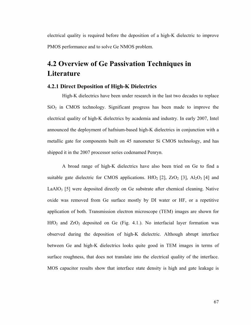
67
electrical quality is required before the deposition of a high-K dielectric to improve
PMOS performance and to solve Ge NMOS problem.
4.2 Overview of Ge Passivation Techniques in Literature
4.2.1 Direct Deposition of High-K Dielectrics High-K dielectrics have been under research in the last two decades to replace
SiO2 in CMOS technology. Significant progress has been made to improve the
electrical quality of high-K dielectrics by academia and industry. In early 2007, Intel
announced the deployment of hafnium-based high-K dielectrics in conjunction with a
metallic gate for components built on 45 nanometer Si CMOS technology, and has
shipped it in the 2007 processor series codenamed Penryn.
A broad range of high-K dielectrics have also been tried on Ge to find a
suitable gate dielectric for CMOS applications. HfO2 [2], ZrO2 [3], Al2O3 [4] and
LaAlO3 [5] were deposited directly on Ge substrate after chemical cleaning. Native
oxide was removed from Ge surface mostly by DI water or HF, or a repetitive
application of both. Transmission electron microscope (TEM) images are shown for
HfO2 and ZrO2 deposited on Ge (Fig. 4.1.). No interfacial layer formation was
observed during the deposition of high-K dielectric. Although abrupt interface
between Ge and high-K dielectrics looks quite good in TEM images in terms of
surface roughness, that does not translate into the electrical quality of the interface.
MOS capacitor results show that interface state density is high and gate leakage is
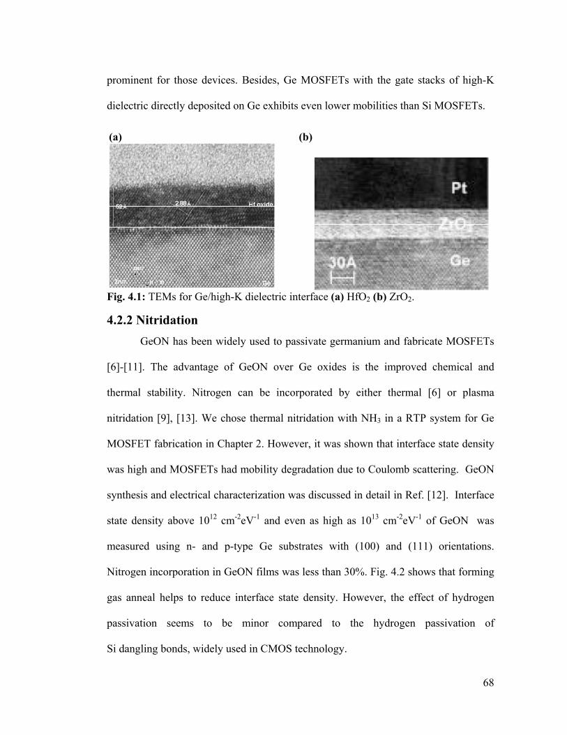
68
prominent for those devices. Besides, Ge MOSFETs with the gate stacks of high-K
dielectric directly deposited on Ge exhibits even lower mobilities than Si MOSFETs.
(a) (b)
Fig. 4.1: TEMs for Ge/high-K dielectric interface (a) HfO2 (b) ZrO2.
4.2.2 Nitridation GeON has been widely used to passivate germanium and fabricate MOSFETs
[6]-[11]. The advantage of GeON over Ge oxides is the improved chemical and
thermal stability. Nitrogen can be incorporated by either thermal [6] or plasma
nitridation [9], [13]. We chose thermal nitridation with NH3 in a RTP system for Ge
MOSFET fabrication in Chapter 2. However, it was shown that interface state density
was high and MOSFETs had mobility degradation due to Coulomb scattering. GeON
synthesis and electrical characterization was discussed in detail in Ref. [12]. Interface
state density above 1012 cm-2eV-1 and even as high as 1013 cm-2eV-1 of GeON was
measured using n- and p-type Ge substrates with (100) and (111) orientations.
Nitrogen incorporation in GeON films was less than 30%. Fig. 4.2 shows that forming
gas anneal helps to reduce interface state density. However, the effect of hydrogen
passivation seems to be minor compared to the hydrogen passivation of
Si dangling bonds, widely used in CMOS technology.
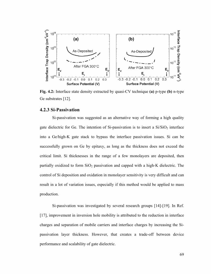
69
Fig. 4.2: Interface state density extracted by quasi-CV technique (a) p-type (b) n-type
Ge substrates [12].
4.2.3 Si-Passivation Si-passivation was suggested as an alternative way of forming a high quality
gate dielectric for Ge. The intention of Si-passivation is to insert a Si/SiO2 interface
into a Ge/high-K gate stack to bypass the interface passivation issues. Si can be
successfully grown on Ge by epitaxy, as long as the thickness does not exceed the
critical limit. Si thicknesses in the range of a few monolayers are deposited, then
partially oxidized to form SiO2 passivation and capped with a high-K dielectric. The
control of Si deposition and oxidation in monolayer sensitivity is very difficult and can
result in a lot of variation issues, especially if this method would be applied to mass
production.
Si-passivation was investigated by several research groups [14]-[19]. In Ref.
[17], improvement in inversion hole mobility is attributed to the reduction in interface
charges and separation of mobile carriers and interface charges by increasing the Si-
passivation layer thickness. However, that creates a trade-off between device
performance and scalability of gate dielectric.
(a) (b)
70
Detailed interface state characterizations revealed asymmetric interface state
density distribution across Ge bandgap (Fig. 4.3). Interface state density reaches 1014
cm-2eV-1 close to conduction band edge [19]. That is a potential problem which can
degrade Ge NMOS inversion formation and drive currents. Hence, Ge NMOS devices
fabricated using this passivation technique exhibited electron mobility less than 100
cm2/Vs.
Fig. 4.3: Interface state density extracted by conducatnce technique, showing very
asymmetric distribution across Ge bandgap [19].
4.2.4 Sulfur Passivation Sulfur was proposed as strong passivant to prevent uncontrolled interface
reactions [20]-[23]. Sulfur is an attractive passivant, since it electrically passivates III-
V compound surfaces [21] and polycrystalline Ge [22]. Sulfur passivation was
achieved using aqueous ammonium sulfide [20]. The sulfur passivation layer was
preserved after the atomic layer deposition of HfO2, acting like a barrier between Ge
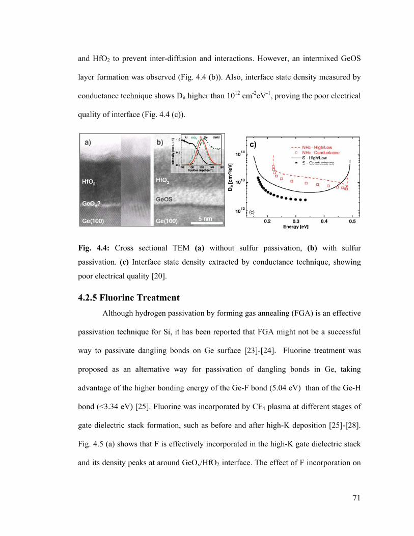
71
and HfO2 to prevent inter-diffusion and interactions. However, an intermixed GeOS
layer formation was observed (Fig. 4.4 (b)). Also, interface state density measured by
conductance technique shows Dit higher than 1012 cm-2eV-1, proving the poor electrical
quality of interface (Fig. 4.4 (c)).
Fig. 4.4: Cross sectional TEM (a) without sulfur passivation, (b) with sulfur
passivation. (c) Interface state density extracted by conductance technique, showing
poor electrical quality [20].
4.2.5 Fluorine Treatment Although hydrogen passivation by forming gas annealing (FGA) is an effective
passivation technique for Si, it has been reported that FGA might not be a successful
way to passivate dangling bonds on Ge surface [23]-[24]. Fluorine treatment was
proposed as an alternative way for passivation of dangling bonds in Ge, taking
advantage of the higher bonding energy of the Ge-F bond (5.04 eV) than of the Ge-H
bond (<3.34 eV) [25]. Fluorine was incorporated by CF4 plasma at different stages of
gate dielectric stack formation, such as before and after high-K deposition [25]-[28].
Fig. 4.5 (a) shows that F is effectively incorporated in the high-K gate dielectric stack
and its density peaks at around GeOx/HfO2 interface. The effect of F incorporation on
c)
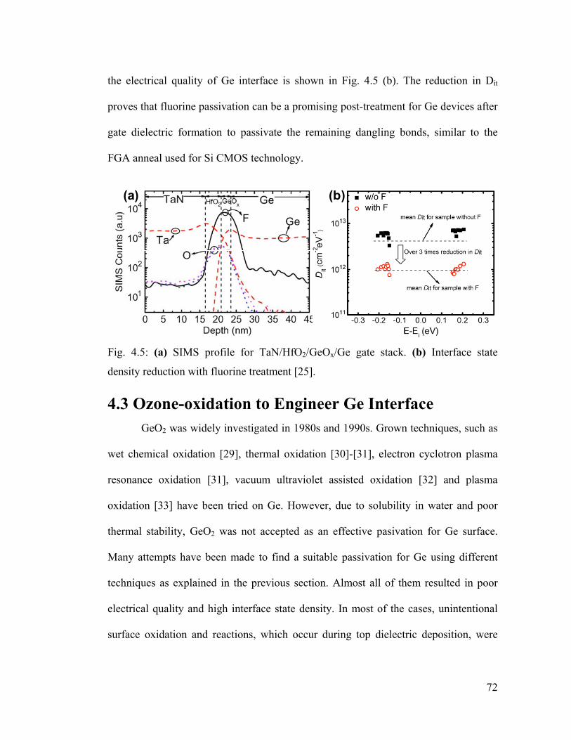
72
the electrical quality of Ge interface is shown in Fig. 4.5 (b). The reduction in Dit
proves that fluorine passivation can be a promising post-treatment for Ge devices after
gate dielectric formation to passivate the remaining dangling bonds, similar to the
FGA anneal used for Si CMOS technology.
Fig. 4.5: (a) SIMS profile for TaN/HfO2/GeOx/Ge gate stack. (b) Interface state
density reduction with fluorine treatment [25].
4.3 Ozone-oxidation to Engineer Ge Interface GeO2 was widely investigated in 1980s and 1990s. Grown techniques, such as
wet chemical oxidation [29], thermal oxidation [30]-[31], electron cyclotron plasma
resonance oxidation [31], vacuum ultraviolet assisted oxidation [32] and plasma
oxidation [33] have been tried on Ge. However, due to solubility in water and poor
thermal stability, GeO2 was not accepted as an effective pasivation for Ge surface.
Many attempts have been made to find a suitable passivation for Ge using different
techniques as explained in the previous section. Almost all of them resulted in poor
electrical quality and high interface state density. In most of the cases, unintentional
surface oxidation and reactions, which occur during top dielectric deposition, were
(a) (b)
73
responsible for the poor interface quality. However, GeO2 is the most native material
to passivate Ge. A thin native oxide layer, around 1 nm thick, can easily grow even
when Ge is exposed to air. GeO2 can effectively passivate Ge surface similar to SiO2
passivation of Si surface, if its growth is well-controlled.
We propose ozone-oxidation to grow GeO2 thermally. Ozone can be helpful in
thermal oxidation of Ge at lower temperatures because it is more reactive than oxygen.
High oxidation temperatures are not preferred because of thermal stability problem.
Also it has been shown for Si that ozone oxidation at lower temperatures results in
lower density of intermediate oxide states [34].
4.3.1 Ozone-oxidation System Ozone-oxidation is proposed for interfacial passivation before the deposition of
high-K dielectric. In order to preserve the layer quality, interfacial passivation layer
has to be in-situ grown right before high-K dielectric deposition. Therefore, atomic
layer deposition (ALD) system, used for high-K dielectric deposition, was modified to
perform controlled ozone-oxidation of Ge. The ALD system was converted from a
Spectrum Model 202 W-CVD system. The schematic of the ALD system is shown in
Fig. 4.6. It is a single wafer equipment with a loadlock. Sample is heated from the
backside up to a maximum temperature of 700 ºC. The sample is held upside down
against quartz window with thermocouples contacting the sample from backside. The
thermocouples read the temperature continuously during the process.
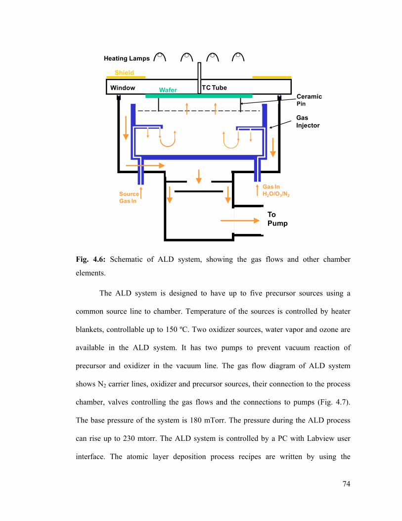
74
Fig. 4.6: Schematic of ALD system, showing the gas flows and other chamber
elements.
The ALD system is designed to have up to five precursor sources using a
common source line to chamber. Temperature of the sources is controlled by heater
blankets, controllable up to 150 ºC. Two oxidizer sources, water vapor and ozone are
available in the ALD system. It has two pumps to prevent vacuum reaction of
precursor and oxidizer in the vacuum line. The gas flow diagram of ALD system
shows N2 carrier lines, oxidizer and precursor sources, their connection to the process
chamber, valves controlling the gas flows and the connections to pumps (Fig. 4.7).
The base pressure of the system is 180 mTorr. The pressure during the ALD process
can rise up to 230 mtorr. The ALD system is controlled by a PC with Labview user
interface. The atomic layer deposition process recipes are written by using the
SourceGas In
Gas InH2O/O3/N2
To Pump
Window Wafer
Shield
Heating Lamps
TC TubeCeramicPin
Gas Injector
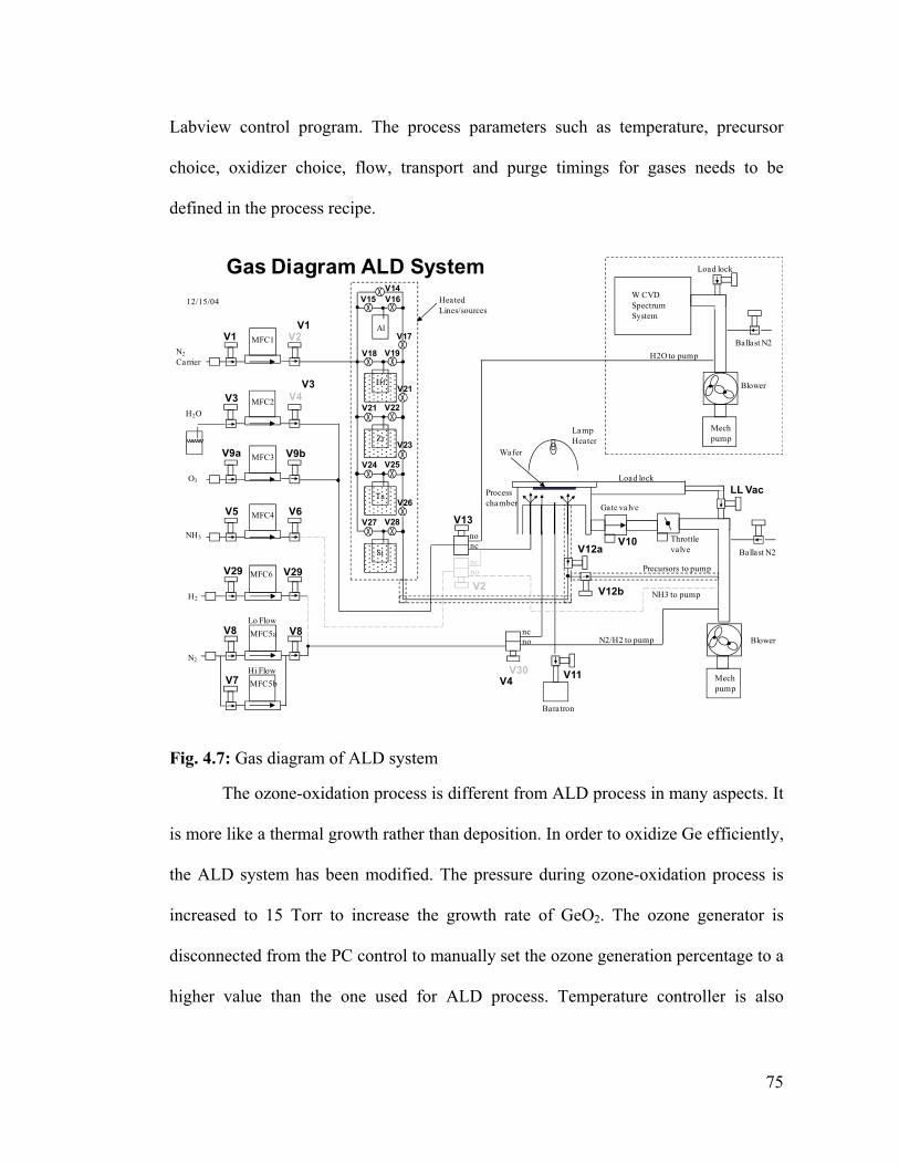
75
Labview control program. The process parameters such as temperature, precursor
choice, oxidizer choice, flow, transport and purge timings for gases needs to be
defined in the process recipe.
Fig. 4.7: Gas diagram of ALD system
The ozone-oxidation process is different from ALD process in many aspects. It
is more like a thermal growth rather than deposition. In order to oxidize Ge efficiently,
the ALD system has been modified. The pressure during ozone-oxidation process is
increased to 15 Torr to increase the growth rate of GeO2. The ozone generator is
disconnected from the PC control to manually set the ozone generation percentage to a
higher value than the one used for ALD process. Temperature controller is also
MFC1N2Carrier
Throttlevalve
Gate valve
Processchamber
LampHeater
Load lock
. . Blower
Mechpump
. . Blower
W CVD SpectrumSystem
Mechpump
Ballast N2
Ballast N2
Wafer
Al
Load lock
12/15/04
MFC2
MFC3
H2O
O3
MFC4
MFC5a
N2
NH3
MFC5bHi Flow
Lo Flow
Hf
HeatedLines/sources
V1 V2
V3 V4
V9a V9b
V5 V6
V8 V8
V7
Baratron
V11
V10
LL Vac
V12a
V12b
no
no
nc
nc
V14V16V15
V17
V18 V19
V21
V21 V22
V24 V25
V23
V26
V27 V28
Zr
Ta
Si
MFC6V29 V29
H2
nonc
V13
V30
V2
V1
H2O to pump
N2/H2 to pump
NH3 to pump
Precursors to pump
V3
V4
Gas Diagram ALD System
76
reprogrammed for the suitable ramp-up speed for Ge wafers, considering thermal
conductivity and expansion coefficient parameters of Ge.
4.3.2 MOSCAP Fabrication We have investigated Ge/GeO2 interface using ozone oxidation of Ge. MOS
capacitors (MOSCAPs) were built on n-type Ge substrates with (100) surface
orientation. Ge wafers were thermally oxidized with ozone at 15 Torr in the 200-450
°C range to form a passivating interlayer. Oxidation was followed by depositions of
either SiO2 or HfO2 on different samples. LPCVD SiO2 was deposited at 300 °C
followed by Al sputtering and photolithography to make the MOSCAP patterns. HfO2
was deposited by ALD at 150°C with precursor tetradiethylaminohafnium (TDEAH)
and Pt was evaporated using shadow masking to form the gate electrodes.
4.3.3 Interface Characterization with Low-T Conductance Technique In the MOS capacitor study, to target Ge NMOS problem we focused on n-
type substrate and measured Dit in the upper half of the bandgap. Dit distribution for
various samples is shown in Fig. 4.8. Conductance method is a reliable way to extract
Dit but it cannot be directly applied to Ge. At room temperature, due to thermal
generation and weak inversion response, conductance does not exhibit typical
interface trap behavior. Time constants for capture and emission processes of carriers
through interface traps are much shorter for Ge than for Si, due to smaller bandgap.
Hence, the conductance was measured in the temperature range of 77-250 K, to
determine Dit distribution across the bandgap and close to band edges, as explained in
Chapter 3.
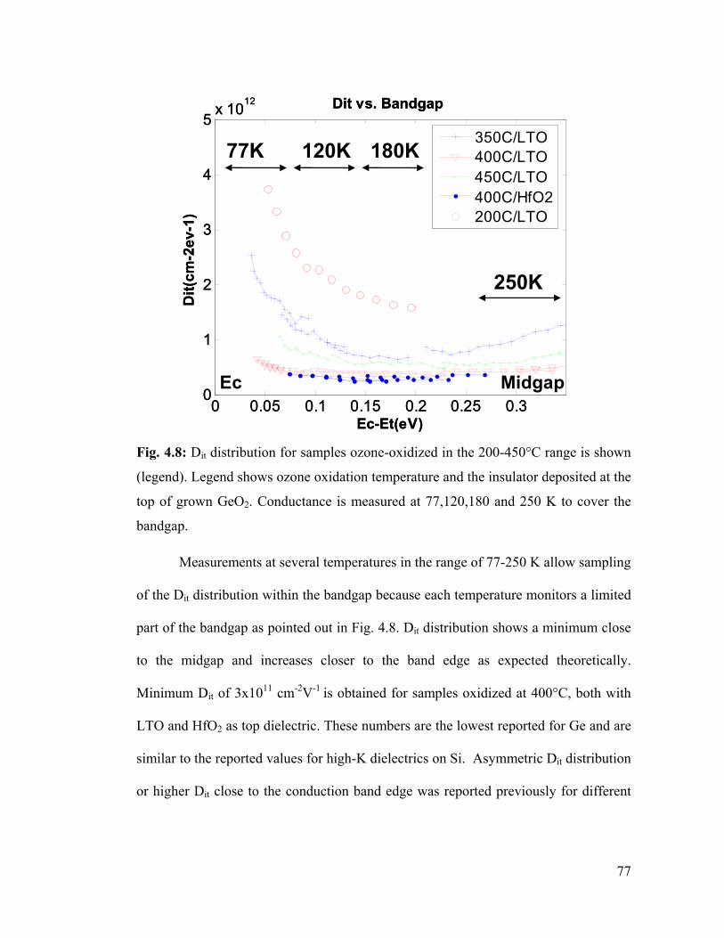
77
Fig. 4.8: Dit distribution for samples ozone-oxidized in the 200-450°C range is shown
(legend). Legend shows ozone oxidation temperature and the insulator deposited at the
top of grown GeO2. Conductance is measured at 77,120,180 and 250 K to cover the
bandgap.
Measurements at several temperatures in the range of 77-250 K allow sampling
of the Dit distribution within the bandgap because each temperature monitors a limited
part of the bandgap as pointed out in Fig. 4.8. Dit distribution shows a minimum close
to the midgap and increases closer to the band edge as expected theoretically.
Minimum Dit of 3x1011 cm-2V-1 is obtained for samples oxidized at 400°C, both with
LTO and HfO2 as top dielectric. These numbers are the lowest reported for Ge and are
similar to the reported values for high-K dielectrics on Si. Asymmetric Dit distribution
or higher Dit close to the conduction band edge was reported previously for different
0 0.05 0.1 0.15 0.2 0.25 0.30
1
2
3
4
5x 10¹²
Ec-Et(eV)
Dit(
cm-2
ev-1
)
Dit vs. Bandgap
350C/LTO400C/LTO450C/LTO400C/HfO2200C/LTO
77K 120K 180K
Ec Midgap
250K
0 0.05 0.1 0.15 0.2 0.25 0.30
1
2
3
4
5x 10¹²
Ec-Et(eV)
Dit(
cm-2
ev-1
)
Dit vs. Bandgap
350C/LTO400C/LTO450C/LTO400C/HfO2200C/LTO
77K 120K 180K
Ec Midgap
250K
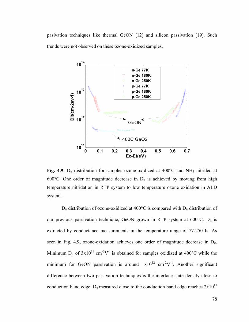
78
pasivation techniques like thermal GeON [12] and silicon passivation [19]. Such
trends were not observed on these ozone-oxidized samples.
Fig. 4.9: Dit distribution for samples ozone-oxidized at 400°C and NH3 nitrided at
600°C. One order of magnitude decrease in Dit is achieved by moving from high
temperature nitridation in RTP system to low temperature ozone oxidation in ALD
system.
Dit distribution of ozone-oxidized at 400°C is compared with Dit distribution of
our previous passivation technique, GeON grown in RTP system at 600°C. Dit is
extracted by conductance measurements in the temperature range of 77-250 K. As
seen in Fig. 4.9, ozone-oxidation achieves one order of magnitude decrease in Dit.
Minimum Dit of 3x1011 cm-2V-1 is obtained for samples oxidized at 400°C while the
minimum for GeON passivation is around 1x1012 cm-2V-1. Another significant
difference between two passivation techniques is the interface state density close to
conduction band edge. Dit measured close to the conduction band edge reaches 2x10¹³
0 0.1 0.2 0.3 0.4 0.5 0.6 0.710
11
1012
1013
1014
Ec-Et(eV)
D
it(cm
-2ev
-1)
n-Ge 77Kn-Ge 180Kn-Ge 250Kp-Ge 77Kp-Ge 180Kp-Ge 250K
400C GeO2
GeON
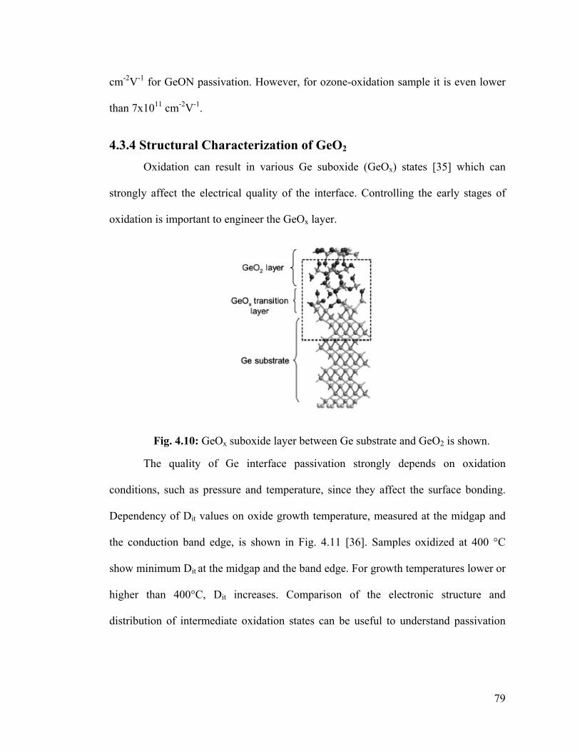
79
cm-2V-1 for GeON passivation. However, for ozone-oxidation sample it is even lower
than 7x1011 cm-2V-1.
4.3.4 Structural Characterization of GeO2
Oxidation can result in various Ge suboxide (GeOx) states [35] which can
strongly affect the electrical quality of the interface. Controlling the early stages of
oxidation is important to engineer the GeOx layer.
Fig. 4.10: GeOx suboxide layer between Ge substrate and GeO2 is shown.
The quality of Ge interface passivation strongly depends on oxidation
conditions, such as pressure and temperature, since they affect the surface bonding.
Dependency of Dit values on oxide growth temperature, measured at the midgap and
the conduction band edge, is shown in Fig. 4.11 [36]. Samples oxidized at 400 °C
show minimum Dit at the midgap and the band edge. For growth temperatures lower or
higher than 400°C, Dit increases. Comparison of the electronic structure and
distribution of intermediate oxidation states can be useful to understand passivation
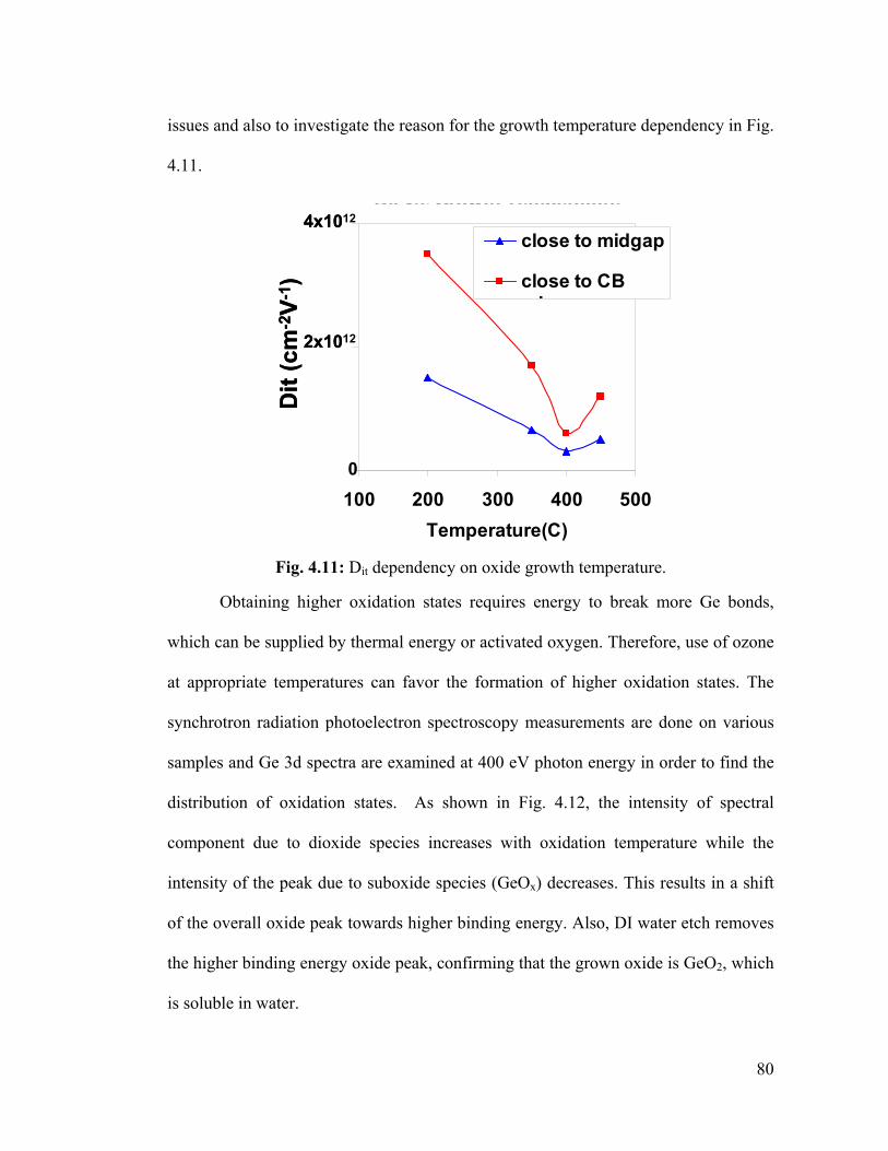
80
issues and also to investigate the reason for the growth temperature dependency in Fig.
4.11.
Fig. 4.11: Dit dependency on oxide growth temperature.
Obtaining higher oxidation states requires energy to break more Ge bonds,
which can be supplied by thermal energy or activated oxygen. Therefore, use of ozone
at appropriate temperatures can favor the formation of higher oxidation states. The
synchrotron radiation photoelectron spectroscopy measurements are done on various
samples and Ge 3d spectra are examined at 400 eV photon energy in order to find the
distribution of oxidation states. As shown in Fig. 4.12, the intensity of spectral
component due to dioxide species increases with oxidation temperature while the
intensity of the peak due to suboxide species (GeOx) decreases. This results in a shift
of the overall oxide peak towards higher binding energy. Also, DI water etch removes
the higher binding energy oxide peak, confirming that the grown oxide is GeO2, which
is soluble in water.
Dit vs. Growth Temperature
100 200 300 400 500Temperature(C)
close to midgap
close to CBd
4x10¹²
2x10¹²
0
Dit
(cm
-2V-
1 )
Dit vs. Growth Temperature
100 200 300 400 500Temperature(C)
close to midgap
close to CBd
4x10¹²
2x10¹²
0
Dit
(cm
-2V-
1 )
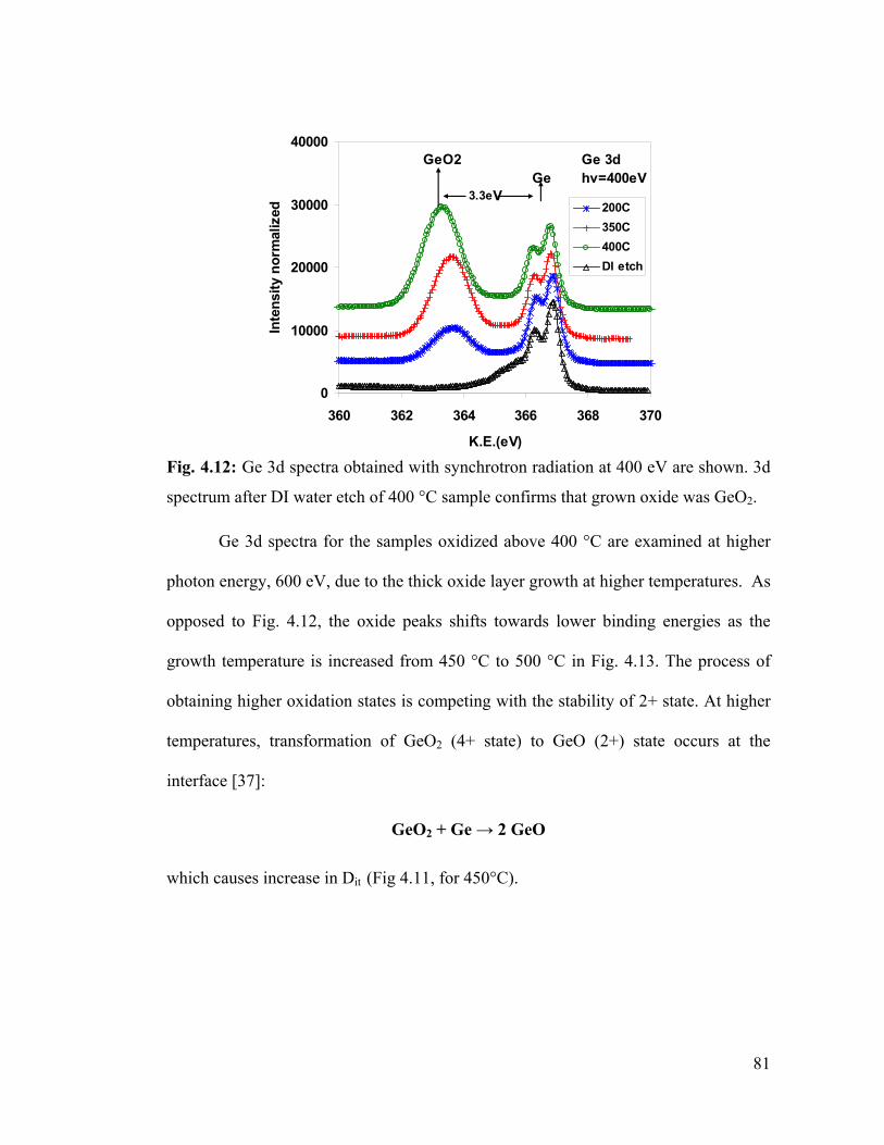
81
Fig. 4.12: Ge 3d spectra obtained with synchrotron radiation at 400 eV are shown. 3d
spectrum after DI water etch of 400 °C sample confirms that grown oxide was GeO2.
Ge 3d spectra for the samples oxidized above 400 °C are examined at higher
photon energy, 600 eV, due to the thick oxide layer growth at higher temperatures. As
opposed to Fig. 4.12, the oxide peaks shifts towards lower binding energies as the
growth temperature is increased from 450 °C to 500 °C in Fig. 4.13. The process of
obtaining higher oxidation states is competing with the stability of 2+ state. At higher
temperatures, transformation of GeO2 (4+ state) to GeO (2+) state occurs at the
interface [37]:
GeO2 + Ge → 2 GeO
which causes increase in Dit (Fig 4.11, for 450°C).
0
10000
20000
30000
40000
360 362 364 366 368 370
K.E.(eV)
Inte
nsity
nor
mal
ized 200C
350C400CDI etch
GeGeO2 Ge 3d
hv=400eV3.3eV
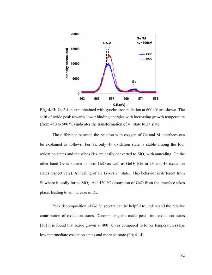
82
Fig. 4.13: Ge 3d spectra obtained with synchrotron radiation at 600 eV are shown. The
shift of oxide peak towards lower binding energies with increasing growth temperature
(from 450 to 500 ºC) indicates the transformation of 4+ state to 2+ state.
The difference between the reaction with oxygen of Ge and Si interfaces can
be explained as follows: For Si, only 4+ oxidation state is stable among the four
oxidation states and the suboxides are easily converted to SiO2 with annealing. On the
other hand Ge is known to form GeO as well as GeO2 (Ge in 2+ and 4+ oxidation
states respectively). Annealing of Ge favors 2+ state. This behavior is different from
Si where it easily forms SiO2. At ~420 °C desorption of GeO from the interface takes
place, leading to an increase in Dit.
Peak decomposition of Ge 3d spectra can be helpful to understand the relative
contribution of oxidation states. Decomposing the oxide peaks into oxidation states
[36] it is found that oxide grown at 400 °C (as compared to lower temperatures) has
less intermediate oxidation states and more 4+ state (Fig 4.14).
0
5000
10000
15000
20000
563 565 567 569 571 573
K.E.(eV)
Inte
nsity
nor
mal
ized
450C500C
Ge
Ge 3dhv=600eV0.2eV
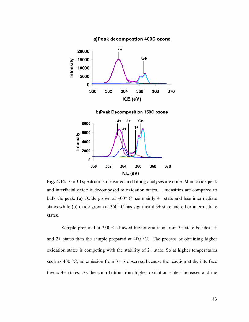
83
Fig. 4.14: Ge 3d spectrum is measured and fitting analyses are done. Main oxide peak
and interfacial oxide is decomposed to oxidation states. Intensities are compared to
bulk Ge peak. (a) Oxide grown at 400° C has mainly 4+ state and less intermediate
states while (b) oxide grown at 350° C has significant 3+ state and other intermediate
states.
Sample prepared at 350 ºC showed higher emission from 3+ state besides 1+
and 2+ states than the sample prepared at 400 °C. The process of obtaining higher
oxidation states is competing with the stability of 2+ state. So at higher temperatures
such as 400 °C, no emission from 3+ is observed because the reaction at the interface
favors 4+ states. As the contribution from higher oxidation states increases and the
a)Peak decompostion 400C ozone
0
5000
10000
15000
20000
360 362 364 366 368 370
K.E.(eV)
Inte
nsity
4+
Ge
b)Peak Decomposition 350C ozone
0
2000
4000
6000
8000
360 362 364 366 368 370K.E.(eV)
Inte
nsity
3+
4+ 2+1+
Ge
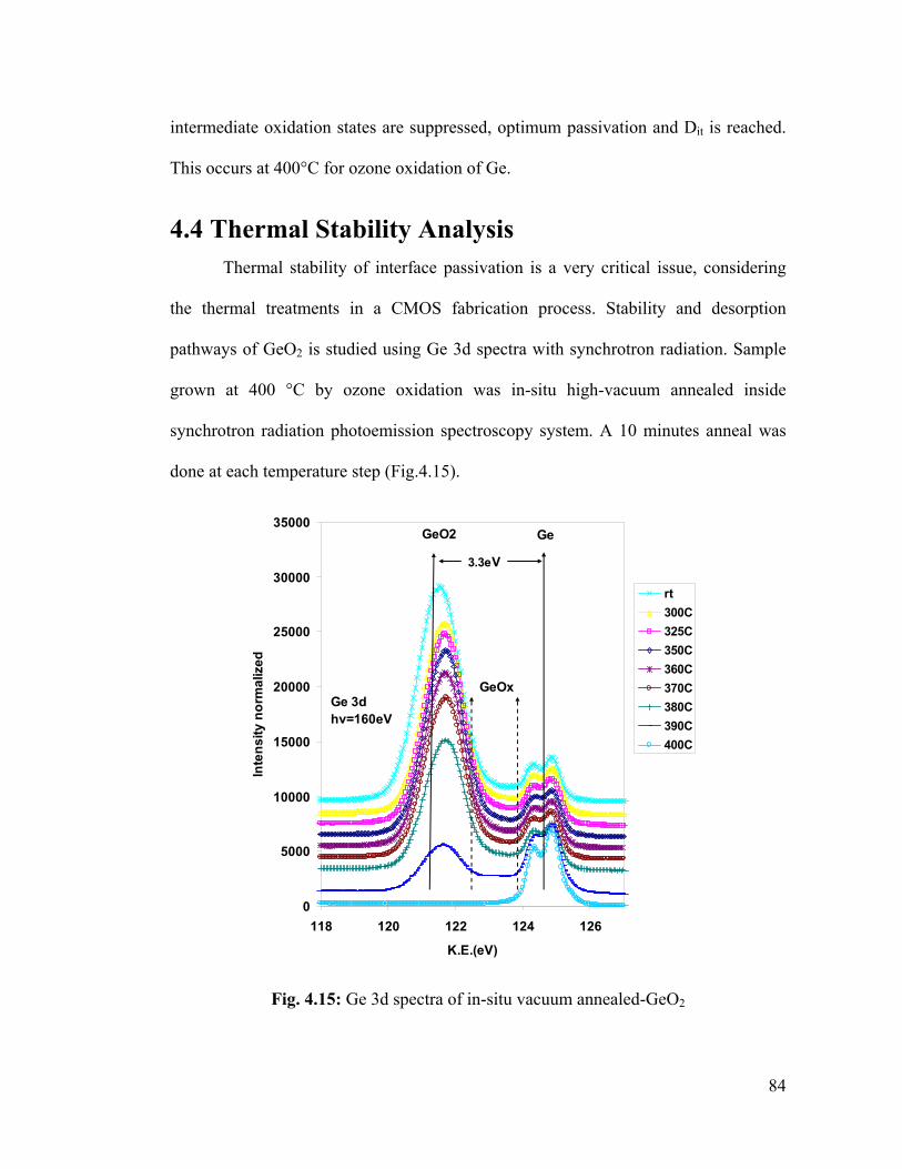
84
intermediate oxidation states are suppressed, optimum passivation and Dit is reached.
This occurs at 400°C for ozone oxidation of Ge.
4.4 Thermal Stability Analysis Thermal stability of interface passivation is a very critical issue, considering
the thermal treatments in a CMOS fabrication process. Stability and desorption
pathways of GeO2 is studied using Ge 3d spectra with synchrotron radiation. Sample
grown at 400 °C by ozone oxidation was in-situ high-vacuum annealed inside
synchrotron radiation photoemission spectroscopy system. A 10 minutes anneal was
done at each temperature step (Fig.4.15).
Fig. 4.15: Ge 3d spectra of in-situ vacuum annealed-GeO2
0
5000
10000
15000
20000
25000
30000
35000
118 120 122 124 126
K.E.(eV)
Inte
nsity
nor
mal
ized
rt300C325C350C360C370C380C390C400C
GeGeO2
Ge 3dhv=160eV
3.3eV
GeOx
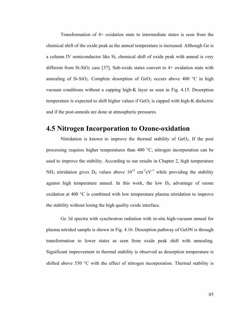
85
Transformation of 4+ oxidation state to intermediate states is seen from the
chemical shift of the oxide peak as the anneal temperature is increased. Although Ge is
a column IV semiconductor like Si, chemical shift of oxide peak with anneal is very
different from Si-SiO2 case [37]. Sub-oxide states convert to 4+ oxidation state with
annealing of Si-SiO2. Complete desorption of GeO2 occurs above 400 °C in high
vacuum conditions without a capping high-K layer as seen in Fig. 4.15. Desorption
temperature is expected to shift higher values if GeO2 is capped with high-K dielectric
and if the post-anneals are done at atmospheric pressures.
4.5 Nitrogen Incorporation to Ozone-oxidation Nitridation is known to improve the thermal stability of GeO2. If the post
processing requires higher temperatures than 400 °C, nitrogen incorporation can be
used to improve the stability. According to our results in Chapter 2, high temperature
NH3 nitridation gives Dit values above 1012 cm-2eV-1 while providing the stability
against high temperature anneal. In this work, the low Dit advantage of ozone
oxidation at 400 °C is combined with low temperature plasma nitridation to improve
the stability without losing the high quality oxide interface.
Ge 3d spectra with synchrotron radiation with in-situ high-vacuum anneal for
plasma nitrided sample is shown in Fig. 4.16. Desorption pathway of GeON is through
transformation to lower states as seen from oxide peak shift with annealing.
Significant improvement in thermal stability is observed as desorption temperature is
shifted above 550 °C with the effect of nitrogen incorporation. Thermal stability is
86
expected to improve more with an oxide cap layer and under normal processing
pressures.
Fig. 4.16: Ge 3d spectra of in-situ vacuum annealed-GeO2
Thermal stability analyses show that plasma nitridation improves the stability
of Ge-insulator interface. However, the electrical quality of the interface is a critical
requirement which needs to be examined for the case of nitrogen incorporation.
Capacitance voltage measurements results of the samples gone through ozone
oxidation and plasma nitridation processes without and with forming gas anneal are
shown in Fig.4.17 (a) and Fig. 4.17 (b) respectively. C-V measurements are done at
233 K to avoid the inversion response. Equivalent oxide thickness extracted from
inversion capacitance is around 2.5 nm. The samples gone through forming gas anneal
0
5000
10000
15000
20000
25000
30000
35000
40000
118 120 122 124 126
K.E.(eV)
Inte
nsity
nor
mal
ized
rt330C370C410C450C500C540C550C560C570C580C590C600C610C
GeGeON
Ge 3dhv=160eV
2.6eV
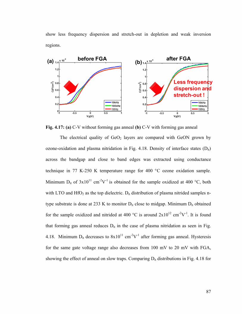
87
show less frequency dispersion and stretch-out in depletion and weak inversion
regions.
Fig. 4.17: (a) C-V without forming gas anneal (b) C-V with forming gas anneal
The electrical quality of GeO2 layers are compared with GeON grown by
ozone-oxidation and plasma nitridation in Fig. 4.18. Density of interface states (Dit)
across the bandgap and close to band edges was extracted using conductance
technique in 77 K-250 K temperature range for 400 °C ozone oxidation sample.
Minimum Dit of 3x1011 cm-2V-1 is obtained for the sample oxidized at 400 °C, both
with LTO and HfO2 as the top dielectric. Dit distribution of plasma nitrided samples n-
type substrate is done at 233 K to monitor Dit close to midgap. Minimum Dit obtained
for the sample oxidized and nitrided at 400 °C is around 2x1012 cm-2V-1. It is found
that forming gas anneal reduces Dit in the case of plasma nitridation as seen in Fig.
4.18. Minimum Dit decreases to 8x1011 cm-2V-1 after forming gas anneal. Hysteresis
for the same gate voltage range also decreases from 100 mV to 20 mV with FGA,
showing the effect of anneal on slow traps. Comparing Dit distributions in Fig. 4.18 for
before FGA after FGA
Less frequency dispersion and stretch-out !
(a) (b)
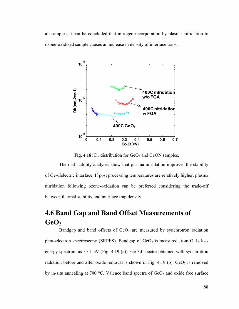
88
all samples, it can be concluded that nitrogen incorporation by plasma nitridation to
ozone-oxidized sample causes an increase in density of interface traps.
Fig. 4.18: Dit distribution for GeO2 and GeON samples.
Thermal stability analyses show that plasma nitridation improves the stability
of Ge-dielectric interface. If post processing temperatures are relatively higher, plasma
nitridation following ozone-oxidation can be preferred considering the trade-off
between thermal stability and interface trap density.
4.6 Band Gap and Band Offset Measurements of GeO2
Bandgap and band offsets of GeO2 are measured by synchrotron radiation
photoelectron spectroscopy (SRPES). Bandgap of GeO2 is measured from O 1s loss
energy spectrum as ~5.1 eV (Fig. 4.19 (a)). Ge 3d spectra obtained with synchrotron
radiation before and after oxide removal is shown in Fig. 4.19 (b). GeO2 is removed
by in-situ annealing at 700 °C. Valence band spectra of GeO2 and oxide free surface
0 0.1 0.2 0.3 0.4 0.5 0.6 0.710
11
1012
1013
Ec-Et(eV)
Dit(
cm-2
ev-1
)
400C GeO2
400C nitridationw/o FGA
400C nitridationw FGA
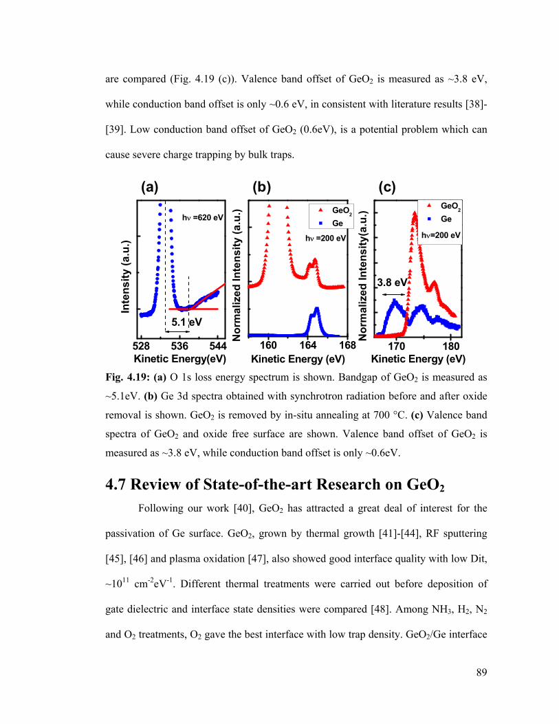
89
are compared (Fig. 4.19 (c)). Valence band offset of GeO2 is measured as ~3.8 eV,
while conduction band offset is only ~0.6 eV, in consistent with literature results [38]-
[39]. Low conduction band offset of GeO2 (0.6eV), is a potential problem which can
cause severe charge trapping by bulk traps.
Fig. 4.19: (a) O 1s loss energy spectrum is shown. Bandgap of GeO2 is measured as
~5.1eV. (b) Ge 3d spectra obtained with synchrotron radiation before and after oxide
removal is shown. GeO2 is removed by in-situ annealing at 700 °C. (c) Valence band
spectra of GeO2 and oxide free surface are shown. Valence band offset of GeO2 is
measured as ~3.8 eV, while conduction band offset is only ~0.6eV.
4.7 Review of State-of-the-art Research on GeO2 Following our work [40], GeO2 has attracted a great deal of interest for the
passivation of Ge surface. GeO2, grown by thermal growth [41]-[44], RF sputtering
[45], [46] and plasma oxidation [47], also showed good interface quality with low Dit,
~1011 cm-2eV-1. Different thermal treatments were carried out before deposition of
gate dielectric and interface state densities were compared [48]. Among NH3, H2, N2
and O2 treatments, O2 gave the best interface with low trap density. GeO2/Ge interface
528 536 544
Inte
nsity
(a.u
.)
Kinetic Energy(eV)
5.1 eV
hν =620 eV
160 164 168
GeO2
GeN
orm
aliz
ed In
tens
ity (a
.u.)
Kinetic Energy (eV)
hν =200 eV
170 180
GeO2
Ge
Nor
mal
ized
Inte
nsity
(a.u
.)Kinetic Energy (eV)
3.8 eV
hν=200 eV
(a) (b) (c)
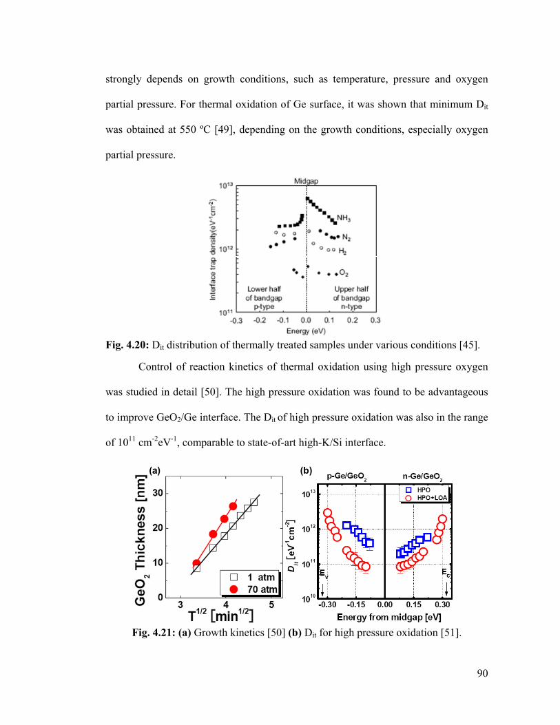
90
strongly depends on growth conditions, such as temperature, pressure and oxygen
partial pressure. For thermal oxidation of Ge surface, it was shown that minimum Dit
was obtained at 550 ºC [49], depending on the growth conditions, especially oxygen
partial pressure.
Fig. 4.20: Dit distribution of thermally treated samples under various conditions [45].
Control of reaction kinetics of thermal oxidation using high pressure oxygen
was studied in detail [50]. The high pressure oxidation was found to be advantageous
to improve GeO2/Ge interface. The Dit of high pressure oxidation was also in the range
of 1011 cm-2eV-1, comparable to state-of-art high-K/Si interface.
Fig. 4.21: (a) Growth kinetics [50] (b) Dit for high pressure oxidation [51].
(a) (b)
91
4.8 Summary In summary, we discussed surface passivation techniques for Ge and electrical
quality of Ge/dielectric interfaces in detail. A new technique to electrically passivate
the interface of Ge using thermal oxidation with ozone prior to a dielectric deposition
has been developed to improve CMOS performance. Dit distributions over the
bandgap and close to band edges were extracted using conductance technique at low
temperatures. A minimum Dit of 3x1011 cm-2 V-1 was obtained for samples oxidized at
400°C in ozone ambient, which is in the range of state-of-the-art Si/High-K dielectric
interface quality. Lower or higher oxidation temperatures than 400°C showed increase
in Dit values due to formation of Ge suboxide (GeOx) states. Physical quality of the
interface was investigated through Ge 3d spectra measurements. We found that the
interface and Dit is strongly affected by the distribution of oxidation states and quality
of the suboxide layer.
4.9 References [1] K. Saraswat, C.O. Chui, K. Donghyun, T. Krishnamohan, A. Pethe, “High
mobility materials and novel device structures for high performance nanoscale
MOSFETs”, IEDM Tech. Dig, pp. 659-662, 2006.
[2] E. P. Gusev, H. Shang, M. Copel, M. Grilbeyuk, C. D’Emic, P. Kozlowski, T.
Zabel, “Microstructure and thermal stability of HfO2 gate dielectric deposited on
Ge(100)”, App. Phys. Lett., 85, pp. 2334-2337, 2004.
92
[3] C. O. Chui, S. Ramanathan, B. B. Triplet, P. C. McIntyre, K. C. Saraswat, “Ge
MOS capacitors incorporating ultrathin High-K gate dielectric”, IEEE Elec. Dev.
Lett., 23, pp. 473-476, 2002.
[4] S. Iwauchi, T. Tanaka, “Interface properties of Al2O3-Ge structure and
characteristics of Al2O3-Ge MOS transistors”, Jpn. J. Appl. Phys., 10, pp. 260-265,
1971.
[5] D. S. Yu, K. C. Chiang, C. F. Cheng, A. Chin, C. Zhu, M. F. Li, D-L. Kwong,
“Fully silicided NiSi:Hf-LaAlO3/SC-GOI n-MOSFETs with high electron
mobility”, IEEE Elec. Dev. Lett., 25, pp. 559-562, 2004.
[6] D. J. Hymes, J. J. Rosenberg, “Growth and materials characterization of native
GeON thin films on germanium”, J. Electrochem. Soc., vol. 135, pp. 961-965,
1988.
[7] J.J Rosenberg, S. C. Martin, “Self-aligned germanium MOSFETs using a nitride
native oxide gate insulator”, IEEE Elec. Dev. Lett., vol. 9, pp. 639-640, 1988.
[8] S. C. Martin, L. M. Hitt, J. J. Rosenberg, “p-channel Ge MOSFETs with high
channel mobility”, IEEE Elec. Dev. Lett., vol. 10, pp. 325-326, 1988
[9] Z. Sun and C. Liu, “Plasma anodic oxidation and nitridation of Ge(111) surface”,
Semicond. Sci. Technol., vol. 8, no. 9, pp. 1779–1782, Sep. 1993.
[10] H. Shang, K-L. Lee, P. Kozlowski, C. D’emic, I. Babich, E. Sikorski, M.
Ieong, H. –S. P. Wong, K. Guarini, W. Haensch, “Self-aligned n-channel
germanium MOSFETs with a thin Ge oxynitride gate dielectric and tungsten gate”,
IEEE Elec. Dev. Lett., 25, pp. 135-138, Mar. 2004.
93
[11] T. Maeda, M. Nishizawa, Y. Morita, “Role of germanium nitride interfacial
layers in HfO2/germanium nitride/germanium metal-insulator-semiconductor
structures”, Appl. Phys. Lett., 90, 072911, Feb. 2007.
[12] C. O. Chui, F. Ito, K. Saraswat, “Nanoscale germanium MOS dielectrics- Part
I: Germanium oxynitrides”, IEEE Trans. Elec. Dev., 53, pp. 1501-1508, July 2006.
[13] Y. Oshima, M. Shandalov, Y. Sun, P. Pianetta, P. C. McIntyre, “Hafnium
oxide/germanium oxynitride gate stacks on germanium: capacitance scaling and
interface state denstity”, Appl. Phys. Lett., 94, 183102, May 2009.
[14] Y. Wang, Y. Z. Hu, E. A. Irene, “In-situ investigation of the passivation of si
and Ge by electron cyclotron resonance plasma enhanced chemical vapor
deposition of SiO2”, J. Vac. Sci. Technol. B, vol.14, pp. 1687-1696,1996.
[15] G. G. Fountain, R. A. Rudder, S. V. Hattangady, D. J. Vitkavage, R. J.
Markunas, J. B. Posthill, “Electrical and microstructural characterization of
ultrathin Si interlayer used in silicon dioxide/germanium-based MIS structure”,
Electron. Lett., vol. 24, pp. 692-694, 1988.
[16] D. J. Vitkavage, G. G. Fountain, R. A. Rudder, S. V. Hattangady, R. J.
Markunas, “Gating of germanium surfaces using pseudomorphic silicon
interlayers”, Appl. Phys. Lett. 53, 692, 1988.
[17] N. Taoka, M. Harada, Y. Yamashita, T. Yamamoto, N. Sugiyama, Shin-ichi
Takagi, “Effects of Si passivation on Ge metal-insulator-semiconductor interface
properties and inversion hole mobility”, Appl. Phys. Lett. 92, 113511, Mar. 2008.
[18] B. De Jaeger , R. Bonzom, F. Leys, O. Richard, J. Van Steenbergen, G.
Winderickx, E. Van Moorhem, G. Raskin, F. Letertre, T. Billon, M. Meuris and
94
M. Heyns, “Optimization of a thin layer epitaxial Si as Ge passivation layer to
demonstrate deep sub-micron n- and p-FETs on Ge-On-Insulator substrates”,
Microelectronic Engineering, 80, pp. 26-29, Jun. 2005.
[19] K. Martens, C. O. Chui, G. Brammertz, B. De Jaeger, D. Kuzum, M. Meuris,
M. Heyns, T. Krishnamohan, K. Saraswat, H. E. Maes, G. Groeseneken, “On the
correct extraction of interface trap density of MOS devices with high-mobility
semiconductor substrates”, IEEE Trans. Elec. Dev., 55, pp. 547-555, Feb. 2008.
[20] M. M. Frank, S. J. Koester, M. Copel, J. A. Ott, V. K. Paruchuri, H. Shang,
“Hafnium oxide gate dielectrics on sulfur-passivated germanium”, Appl. Phys.
Lett., 89, 112905, Sep. 2006.
[21] F. Seker, K. Meeker, T. F. Kuech, A. B. Ellis, Chem. Rev., vol. 100, pp. 2505,
2000.
[22] A. Lamzatouar, O. Palais, O. B. M. Hardouin Duparc, J. Thibault, A. Charai, J.
Mater. Sci., vol. 40, pp. 3163, 2005.
[23] V. V. Afanas’ev, Y. G. Fedorenko, and A. Stesmans, “Interface traps and
dangling-bond defects in (100)Ge/HfO2,” Appl. Phys. Lett., vol. 87, no. 3, p. 032
107, Jul. 2005.
[24] J. R. Weber, A. Janotti, P. Rinke, and C. G. Van de Walle,“Dangling bond
defects and hydrogen passivation in germanium,” Appl. Phys. Lett., vol. 91, no. 14,
p. 142101, Oct. 2007.
[25] R. Xie and C. Zhu, “Effects of sulfur passivation on germanium MOS
capacitors with HfON gate dielectric,” IEEE Elec. Dev. Lett., vol. 28, no. 11, pp.
976–979, Nov. 2007.
95
[26] R. Xie, W. He, M. Yu, and C. Zhu, “Effects of fluorine incorporation and
forming gas annealing on high-k gated germanium metal–oxide–semiconductor
with GeO2 surface passivation,” Appl. Phys. Lett., vol. 93, no. 7, p. 073 504, Aug.
2008.
[27] R. Xie, M. Yu, M. Y. Lai, L. Chan, and C. Zhu, “High-k gate stack on
germanium substrate with fluorine incorporation,” Appl. Phys. Lett., vol. 92, no.
16, p. 163 505, Apr. 2008.
[28] R. L. Xie, T. H. Phung, W. He, M. B.Yu, C. X. Zhu, “Interface-engineered
high-mobility high-K/Ge p-MOSFETs with 1nm equivalent oxide thickness”,
IEEE Trans. Elec. Dev., 56, pp. 1330-1337, Jun. 2009.
[29] O. J. Gregory, E. E. Crisman, L. Pruitt, D. J. Hymes, and J. J.
Rosenberg,“Electrical characterization of some native insulators on germanium,”
in Mater. Res. Soc. Symp. Proc., vol. 76, pp. 307–311, 1987.
[30] M. D. Jack, J. Y. M. Lee, and H. Lefevre, “DLTS measurements of a
germanium MIS interface,” J. Electron. Mater., vol. 10, no. 3, pp. 571–589, 1981.
[31] Y. Wang, Y. Z. Hu, and E. A. Irene, “Electron cyclotron resonance plasma and
thermal oxidation mechanisms of germanium,” J. Vac. Sci. Technol. A, Vac. Surf.
Films, vol. 12, no. 4, pp. 1309–1314, Jul. 1994.
[32] V. Craciun, I. W. Boyd, B. Hutton, and D. Williams, “Characteristics of
dielectric layers grown on Ge by low temperature vacuum ultravioletassisted
oxidation”, Appl. Phys. Lett., vol. 75, no. 9, pp. 1261–1263, Aug. 1999.
[33] R. S. Johnson, H. Niimi, and G. Lucovsky, “New approach for the fabrication
of device-quality Ge/GeO2/SiO2 interfaces using low temperature remote plasma
96
processing,” J. Vac. Sci. Technol. A, Vac. Surf. Films, vol. 18, no. 4, pp. 1230–
1233, Jul. 2000.
[34] S. Ichimura, A. Kurokawa, K. Nakamura, “Ultrathin SiO2 film growth on Si by
highly concentrated ozone”, Thin Solid Films, 377-378, pp.518-524, 2000.
[35] D. Schmeisser, R. D. Schnell, A. Bogen, F. J. Himpsel, D. Rieger, G.
Landgren, J. F. Morar,“Surface oxidation states of Ge”, Surf. Sci., 172, pp. 455-
465, 1986.
[36] D. Kuzum, T. Krishnamohan, A. J. Pethe , A. K. Okyay, Y. Oshima, Y. Sun, J.
P. McVittie, P. A. Pianetta, P. C. McIntyre, K. C. Saraswat, “Ge interface
engineering with ozone-oxidation for low interface state density”, Elec. Dev. Lett.,
29, pp. 328-330, 2008.
[37] K. Prabhakaran, F. Maeda, Y. Watanabe, T. Ogino, “Distintcly different
thermal decomposition pathways of ultrathin oxide layer on Ge and Si surfaces”,
App. Phys. Lett., 76, pp. 2244-2247, 2000.
[38] M. Perego, G. Scarel, M. Fanciulli, I. L. Fedushkin, A. A. Skatova,
“Fabrication of GeO2 layers using a divalent Ge precursor”, Appl. Phys. Lett., vol.
90, 162115, Apr. 2007.
[39] M. Yang, R. Q. Wu, Q. Chen, W. S. Deng, Y. P. Feng, J. W. Chai, J. S. Pan, S.
J. Wang, “Impact of oxide defects on band offset at GeO2/Ge interface”, Appl.
Phys. Lett., vol. 94, 142903, Apr. 2009.
[40] D. Kuzum, A. J. Pethe , T. Krishnamohan, Y. Oshima, Y. Sun, J. P. McVittie,
P. A. Pianetta, P. C. McIntyre, K. C. Saraswat, “Interface-engineered Ge (100)
and (111), N- and P-FETs with high mobility” , IEDM Tech. Dig., pp. 723, 2007.
97
[41] A. Delabie, F. Bellenger, M. Houssa, T. Conard, S. V. Elshocht, M. Caymax,
M. Heyns, and M. Meuris, “Effective electrical passivation of Ge(100) for high-k
gate dielectric layers using germanium oxide,” Appl. Phys. Lett., vol. 91, no. 8, p.
082 904, Aug. 2007.
[42] V. V. Afanas’ev, A. Stesmans, A. Delabie, F. Bellenger, M. Houssa, and M.
Meuris, “Electronic structure of GeO2-passivated interfaces of (100) Ge with
Al2O3 and HfO2,” Appl. Phys. Lett., vol. 92, no. 2, p. 022 109, Jan. 2008.
[43] R. Xie, W. He, M. Yu, and C. Zhu, “Effects of fluorine incorporation and
forming gas annealing on high-k gated germanium metal–oxide–semiconductor
with GeO2 surface passivation,” Appl. Phys. Lett., vol. 93, no. 7, p. 073 504, Aug.
2008.
[44] H. Matsubara, T. Sasada, M. Takenaka, and S. Takagi, “Evidence of low
interface trap density in GeO2/Ge metal–oxide–semiconductor structures
fabricated by thermal oxidation,” Appl. Phys. Lett., vol. 93, no. 3, p. 032 104, Jul.
2008.
[45] T. Takahashi, T. Nishimura, L. Chen, S. Sakata, K. Kita, and A. Toriumi,
“Proof of Ge-interfacing concepts for metal/high-k/Ge CMOS—Ge-intimate
material selection and interface conscious process flow”, IEDM Tech. Dig., pp.
697–700, 2007.
[46] K. Kita, S. Suzuki, H. Nomura, T. Takahashi, T. Nishimura, and A. Toriumi,
“Direct evidence of GeO volatilization from GeO2/Ge and impact of its
suppression on GeO2/Ge metal–insulator–semiconductor characteristics,” Jpn. J.
Appl. Phys., vol. 47, no. 4, pp. 2349–2353, 2008.
98
[47] M. Kobayashi, T. Irisawa, B. M. Kope, Y. Sun, K. Saraswat, H.-S. P. Wong, P.
Pianetta, Y. Nishi, “High quality GeO2/Ge interface formed by SPA radical
oxidation and uniaxial stress engineering for high performance Ge NMOSFETs,
VLSI Symposium Digest, pp. 76-77, 2009.
[48] S. Takagi, T. Maeda, N. Taoka, M. Nishizawa, Y. Morita, K. Ikeda, Y.
Yamashita, M. Nishikawa, H. Kumagai, R. Nakane, S. Sugahara, N. Sugiyama,
“Gate dielectric formation and MIS interface characterization on Ge”,
Microelectronic Engineering, 84, pp. 2314-2319, Sep. 2007.
[49] Y. Nakakita, R. Nakane, T. Sasada, H. Matsubara, M. Takaneka, S. Takagi,
“Interface-controlled self-align source/drain Ge pMOSFETs using thermally-
oxidized GeO2 interfacial layers”, IEDM Tech. Dig., 2008.
[50] C. H. Lee, T. Nishimura, K. Nagashio, K. Kita, A. Toriumi, “Reaction kinetics
control on thermal oxidation process of Ge in high pressure oxygen”, SSDM Dig.,
pp. 16-17, 2008.
[51] C. H. Lee, T. Nishimura, T. Tabata, K. Nagashio, K. Kita, A. Toriumi, “High
electron mobility Ge n-channel MOSFETs with GeO2 grown by high pressure
oxidation” SSDM Dig., pp. 1000-1001, 2009.

99
100
Chapter 5 High Mobility Ge NMOS
5.1 Introduction Ge has become of great interest as a channel material for future technology
nodes, owing to its high bulk electron and hole mobilities. Ge P-MOSFETs with
mobilities above 300cm2V-1s-1 have been reported [1], [2]. Ge has a small hole
conductivity effective mass and hence can achieve higher inversion hole mobility.
High density of states (DOS) of Ge allows for it to support channel charge in its higher
mobility valleys even with strong quantization attributed either to the spatial quantum
confinement or to the high electric field. This makes Ge an attractive channel material
for future high-performance N-MOSFETs. However, Ge N-MOSFETs have exhibited
poor drive currents and low mobility, as reported by several different research groups
worldwide [2]-[4]. In spite of the increasing interest in Ge, the sources and the
mechanisms of poor Ge NMOS performance have not been completely clarified yet.
Passivation of Ge interface and activation of n-type dopants have been considered
among major challenges to achieve high performance Ge CMOS.
101
In this chapter, we present Ge NMOS fabricated with the ozone-oxidation and
the low temperature S/D activation processes, achieving the highest electron mobility
to-date. Detailed interface characterization, trapping analyses and gated Hall device
measurements are performed to identify the mechanisms behind poor Ge NMOS
performance in the past. The effects of fast trapping by interface states, slow trapping
by bulk traps and source/drain parasitic resistance on mobility measurements are
discussed. Future directions are pointed out to further improve Ge NMOS
performance.
5.2 Overview of Ge NMOS Results in Literature The intrinsic mobility of carriers in Ge is substantially higher than in Si and is
more symmetric.
Intrinsic bulk mobilities in Ge
Electron - 3900 cm2/Vs
Hole - 1900 cm2/Vs
However, that has not translated into inversion mobility results. Fig. 5.1 show
the inversion mobilties reported using different Al2O3 (Fig. 5.1 (a)) and HfO2 (Fig. 5.1
(b)) as gate dielectrics. PMOS inversion mobilities do not look outstanding and
NMOS shows inversion mobility even lower than Si universal. In Fig. 5.2 (a), PMOS
inversion mobility, measured on Ge PMOS fabricated using GeON passivation [5],
seems to be higher than universal Si mobility. That result is consistent with what we
measured on PMOS devices as discussed in Chapter 2. However, NMOS inversion
mobility with similar passivation exhibits very low inversion mobility in Fig. 5.2 (b)
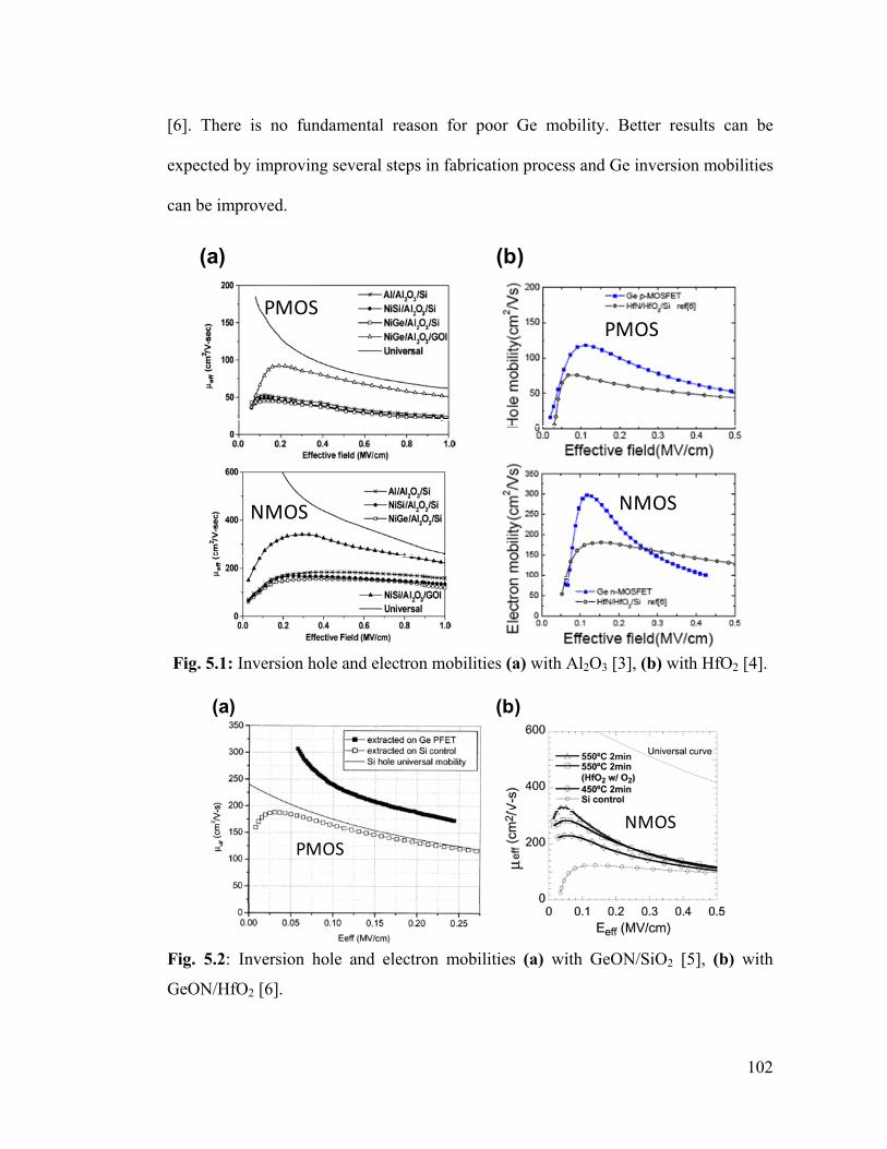
102
[6]. There is no fundamental reason for poor Ge mobility. Better results can be
expected by improving several steps in fabrication process and Ge inversion mobilities
can be improved.
Fig. 5.1: Inversion hole and electron mobilities (a) with Al2O3 [3], (b) with HfO2 [4].
Fig. 5.2: Inversion hole and electron mobilities (a) with GeON/SiO2 [5], (b) with
GeON/HfO2 [6].
PMOS
NMOS
PMOS
NMOS
(a) (b)
(a) (b)
NMOSPMOS
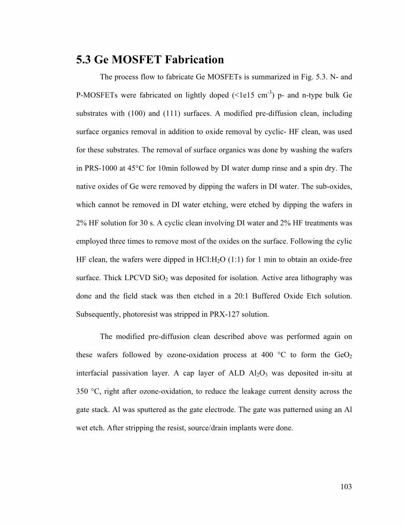
103
5.3 Ge MOSFET Fabrication The process flow to fabricate Ge MOSFETs is summarized in Fig. 5.3. N- and
P-MOSFETs were fabricated on lightly doped (<1e15 cm-3) p- and n-type bulk Ge
substrates with (100) and (111) surfaces. A modified pre-diffusion clean, including
surface organics removal in addition to oxide removal by cyclic- HF clean, was used
for these substrates. The removal of surface organics was done by washing the wafers
in PRS-1000 at 45°C for 10min followed by DI water dump rinse and a spin dry. The
native oxides of Ge were removed by dipping the wafers in DI water. The sub-oxides,
which cannot be removed in DI water etching, were etched by dipping the wafers in
2% HF solution for 30 s. A cyclic clean involving DI water and 2% HF treatments was
employed three times to remove most of the oxides on the surface. Following the cylic
HF clean, the wafers were dipped in HCl:H2O (1:1) for 1 min to obtain an oxide-free
surface. Thick LPCVD SiO2 was deposited for isolation. Active area lithography was
done and the field stack was then etched in a 20:1 Buffered Oxide Etch solution.
Subsequently, photoresist was stripped in PRX-127 solution.
The modified pre-diffusion clean described above was performed again on
these wafers followed by ozone-oxidation process at 400 °C to form the GeO2
interfacial passivation layer. A cap layer of ALD Al2O3 was deposited in-situ at
350 °C, right after ozone-oxidation, to reduce the leakage current density across the
gate stack. Al was sputtered as the gate electrode. The gate was patterned using an Al
wet etch. After stripping the resist, source/drain implants were done.
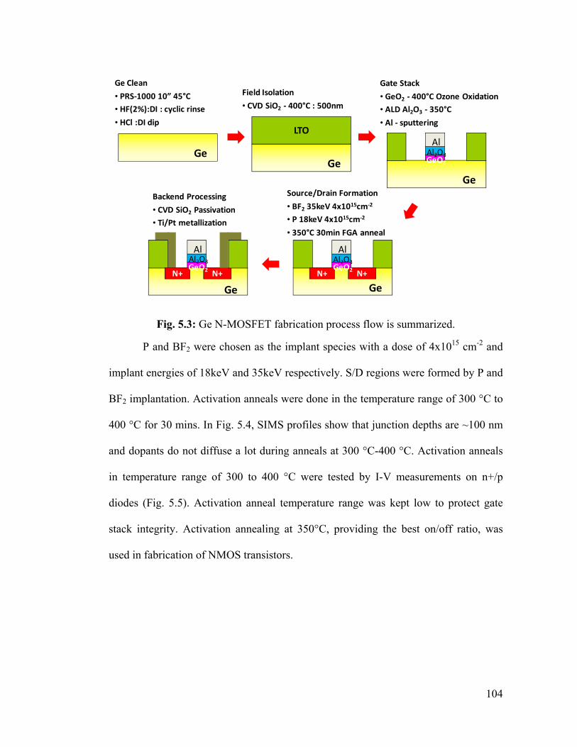
104
Fig. 5.3: Ge N-MOSFET fabrication process flow is summarized.
P and BF2 were chosen as the implant species with a dose of 4x1015 cm-2 and
implant energies of 18keV and 35keV respectively. S/D regions were formed by P and
BF2 implantation. Activation anneals were done in the temperature range of 300 °C to
400 °C for 30 mins. In Fig. 5.4, SIMS profiles show that junction depths are ~100 nm
and dopants do not diffuse a lot during anneals at 300 °C-400 °C. Activation anneals
in temperature range of 300 to 400 °C were tested by I-V measurements on n+/p
diodes (Fig. 5.5). Activation anneal temperature range was kept low to protect gate
stack integrity. Activation annealing at 350°C, providing the best on/off ratio, was
used in fabrication of NMOS transistors.
Ge
Ge Clean
• PRS‐1000 10” 45°C• HF(2%):DI : cyclic rinse• HCl :DI dip
LTO
Ge
Field Isolation
• CVD SiO2 ‐ 400°C : 500nm
Gate Stack
• GeO2 ‐ 400°C Ozone Oxidation• ALD Al2O3 ‐ 350°C
• Al ‐ sputtering
Source/Drain Formation
• BF2 35keV 4x1015cm‐2
• P 18keV 4x1015cm‐2
• 350°C 30min FGA anneal
Backend Processing
• CVD SiO2 Passivation• Ti/Pt metallization
Ge
AlAl2O3GeO2
Ge
Al
N+ N+
Al2O3GeO2
Ge
Al
N+ N+GeO2
Al2O3
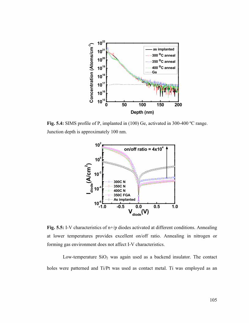
105
Fig. 5.4: SIMS profile of P, implanted in (100) Ge, activated in 300-400 ºC range.
Junction depth is approximately 100 nm.
Fig. 5.5: I-V characteristics of n+/p diodes activated at different conditions. Annealing
at lower temperatures provides excellent on/off ratio. Annealing in nitrogen or
forming gas environment does not affect I-V characteristics.
Low-temperature SiO2 was again used as a backend insulator. The contact
holes were patterned and Ti/Pt was used as contact metal. Ti was employed as an
0 50 100 150 2001015
1016
1017
1018
1019
1020
1021
1022
Con
cent
ratio
n (A
tom
s/cm
-3)
Depth (nm)
as implanted300 oC anneal 350 oC anneal 400 oC anneal Ga
-1.0 -0.5 0.0 0.5 1.010-6
10-4
10-2
100
102
I diod
e(A/c
m2 )
Vdiode(V)
300C N 350C N 400C N 350C FGA As implanted
on/off ratio = 4x10⁴
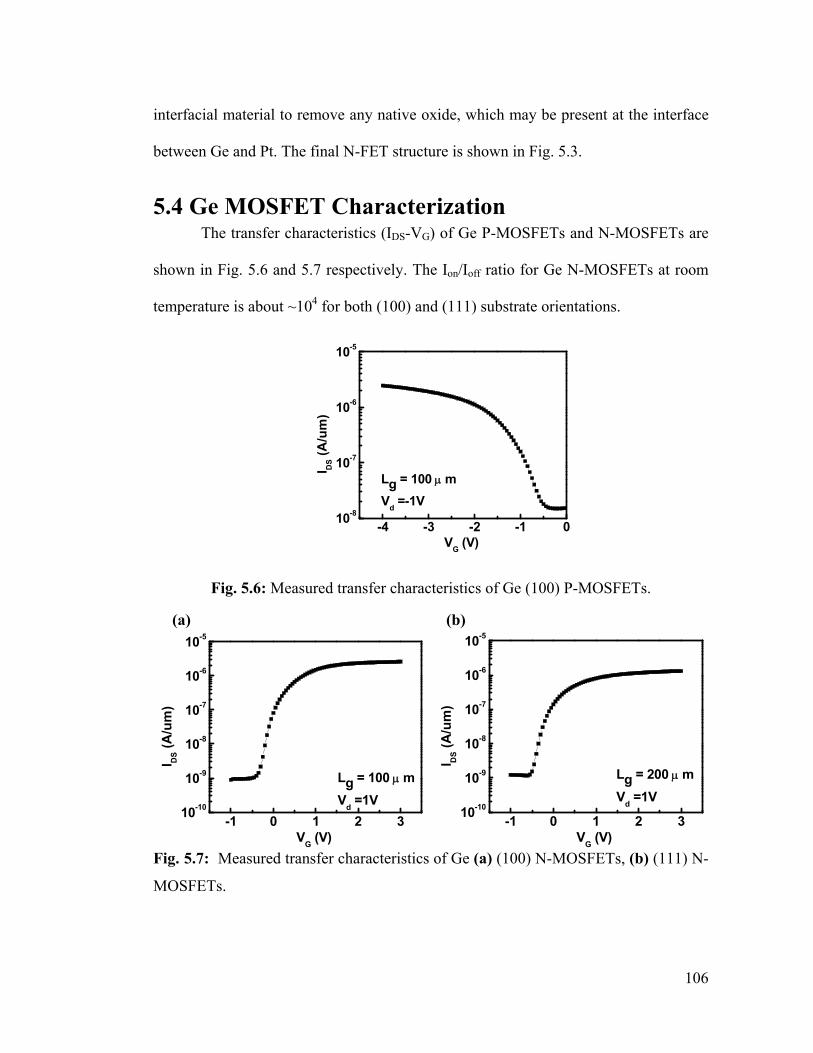
106
interfacial material to remove any native oxide, which may be present at the interface
between Ge and Pt. The final N-FET structure is shown in Fig. 5.3.
5.4 Ge MOSFET Characterization The transfer characteristics (IDS-VG) of Ge P-MOSFETs and N-MOSFETs are
shown in Fig. 5.6 and 5.7 respectively. The Ion/Ioff ratio for Ge N-MOSFETs at room
temperature is about ~104 for both (100) and (111) substrate orientations.
Fig. 5.6: Measured transfer characteristics of Ge (100) P-MOSFETs.
(a) (b)
Fig. 5.7: Measured transfer characteristics of Ge (a) (100) N-MOSFETs, (b) (111) N-
MOSFETs.
-4 -3 -2 -1 010-8
10-7
10-6
10-5
I DS (A
/um
)
VG (V)
Lg = 100 μ mVd =-1V
-1 0 1 2 310-10
10-9
10-8
10-7
10-6
10-5
I DS (
A/u
m)
VG (V)
Lg = 100 μ mVd =1V
-1 0 1 2 310-10
10-9
10-8
10-7
10-6
10-5
I DS (A
/um
)
VG (V)
Lg = 200 μ mVd =1V
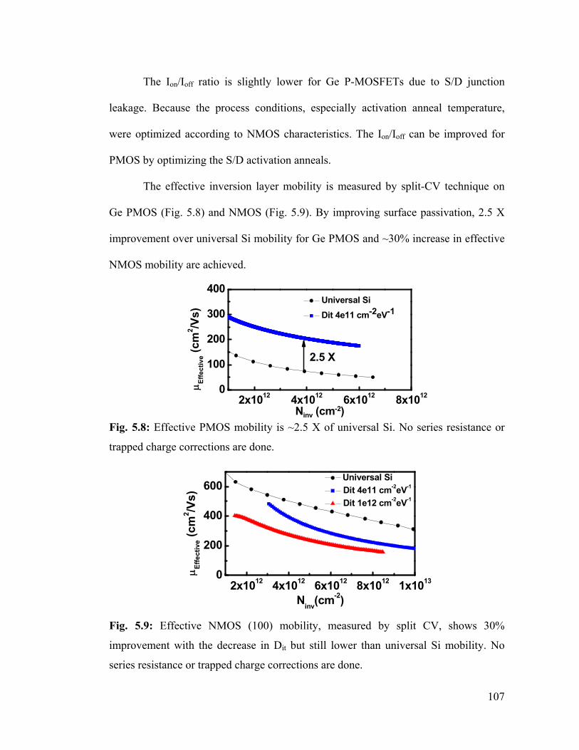
107
The Ion/Ioff ratio is slightly lower for Ge P-MOSFETs due to S/D junction
leakage. Because the process conditions, especially activation anneal temperature,
were optimized according to NMOS characteristics. The Ion/Ioff can be improved for
PMOS by optimizing the S/D activation anneals.
The effective inversion layer mobility is measured by split-CV technique on
Ge PMOS (Fig. 5.8) and NMOS (Fig. 5.9). By improving surface passivation, 2.5 X
improvement over universal Si mobility for Ge PMOS and ~30% increase in effective
NMOS mobility are achieved.
Fig. 5.8: Effective PMOS mobility is ~2.5 X of universal Si. No series resistance or
trapped charge corrections are done.
Fig. 5.9: Effective NMOS (100) mobility, measured by split CV, shows 30%
improvement with the decrease in Dit but still lower than universal Si mobility. No
series resistance or trapped charge corrections are done.
2x10¹² 4x10¹² 6x10¹² 8x10120
100
200
300
400
Universal Si Dit 4e11 cm-2eV-1
μ Effe
ctiv
e (cm
2 /Vs)
Ninv (cm-2)
2.5 X
2x1012 4x10¹² 6x10¹² 8x10¹² 1x10130
200
400
600
Universal Si Dit 4e11 cm-2eV-1
Dit 1e12 cm-2eV-1
μ Effe
ctiv
e (cm
2 /Vs)
Ninv(cm-2)
108
GeO2 has been proposed as interfacial passivation layer before deposition of
high-K dielectric. Its success in passivation of Ge interface and decreasing the density
of interface traps (Dit) was demonstrated [7]. Inspite of the decrease in interface state
density by using ozone-oxidation, effective NMOS mobility improves only 30% and it
is still lower than universal Si mobility (Fig. 5.9). In the next sections, we investigate
the mechanisms behind poor Ge NMOS performance the gate stacks of N- and P-
MOSFETs are characterized in detail to determine the effects of fast and slow traps.
Three mechanisms, fast trapping at Ge/GeO2 interface, slow trapping by GeO2/Al2O3
border traps and parasitic S/D series resistance, are distinguished as degradation
factors for Ge NMOS. Their contributions to the mobility degradation and their
effects on the mobility extraction are evaluated.
5.4.1 Fast Traps The fast traps, so-called interface traps, are located at the
semiconductor/insulator interface. The time constants of the fast traps are so small that
they can be measured at high frequency, such as 1 kHz- 1 MHz range. The magnitude
and the frequency of conductance peaks in the conductance technique measurements
give information on Dit distribution across the bandgap, while the peak frequency on
trap time constant and capture cross section [8]. In MOSFET conductance
measurements, minority carriers can be provided from S/D contacts. Therefore,
conductance response is also observed in inversion regime. However, in conventional
MOSCAP conductance measurements, only majority carriers are responsible for
conductance response and conductance peaks are only observed in depletion regime.
109
The measurable part of Ge bandgap by conductance technique applied to MOSFET
inversion regime is shown in the schematic (Fig. 5.10).
Fig. 5.10: The measureable window of Ge bandgap by conductance technique applied
at NMOS and PMOS inversion regimes.
Conductance measurements were performed on Ge NMOS and PMOS at
230K. Conductance peaks measured in PMOS inversion regime, corresponding to the
valence band side of Ge bandgap, exhibit two distinct sets in different gate voltage
ranges, shown with solid and dashed lines in Fig. 5.11 (a). Time constants extracted
from peak frequency show two distinct types of traps, interacting with majority and
minority bands. That results in the overall time constant behavior in Fig. 5.11 (b).
Fig. 5.11: (a) Conductance peak response for PMOS inversion regime. Two sets of
conductance peaks, corresponding to two types of traps, are observed. The difference
Ec
Ev
Ei
PMOS midgap/inversion
NMOSmidgap/inversion
104
105
106
0
0.2
0.4
0.6
0.8
1
1.2x 10
-6
f(Hz)
Gp/
w(F
/cm
2 )
‐0.84
-0.98
-0.8
-0.62
Two sets of peaks!
Valence Band
-1 -0.8 -0.610
-7
10-6
10-5
10-4
Vg (V)
Tim
e C
onst
ant(s
)
totaltrap Atrap B
Valence Band
Midgap
Two types of traps
(a) (b)
110
in time constants can originate from the existence of donor and acceptor type traps in
the lower half of the bandgap. (b) Time constants of two distinct traps are measured.
As opposed to PMOS, conductance peaks of NMOS inversion regime exhibit
only one set of conductance peaks in [-0.28, 0.02] gate voltage range (Fig. 5.12 (a)).
That corresponds to single type of trap behavior (Fig. 5.12 (b)) in the conduction band
side of the Ge bandgap.
Fig. 5.12: (a) Conductance peak response for NMOS inversion regime. Only single
type of trap behavior is observed. (b) Time constant of single type of trap is measured.
Two types of traps in the valence band side of Ge bandgap is quite unusual, as
opposed to the conventional conductance response known for the traps in Si bandgap.
Similar trap time constant measurements are done on a different sample to ensure that
this phenomenon is not a sample specific issue but a characteristic of Ge. A Ge
MOSCAP sample is prepared by low-temperature HfO2 deposition. The deposition
temperature is kept as low as possible, 150 °C, to avoid interfacial oxide formation
and to keep the surface states arising from dangling bonds. Conductance and time
103
104
105
106
0
0.5
1
1.5
2
2.5x 10
-7
f(Hz)
Gp/
w(F
/cm
2 )
0.02
-0.28
-0.3 -0.2 -0.1 0 0.110
-7
10-6
10-5
10-4
10-3
Vg(V)
Tim
e C
onst
ant(s
)Conduction
Band
Midgap
One set of peaks!
Single trapbehavior
Conduction Band (a) (b)
111
constant measurements were performed on HfO2/Ge interface to confirm that two
types of traps is not sample specific but a property of Ge itself (Fig. 5.13).
Fig. 5.13: Conductance peak response in different gate bias ranges (a) 77 K and (b)
180 K. As temperature is increased to 120 K and 180 K, the trap range visible in 1
kHz-1 MHz shifts away from valence band toward midgap and the conductance peaks
shift to corresponding gate biases.
Gp/w vs f is plotted in Fig 5.13. Two distinct set of conductance peaks are
observed in different voltage ranges. At 77 K, conductance peaks in the [-0.44,-0.5]
voltage range are closer to strong accumulation and consequently to the valence band
edge than the peaks in the [-0.24,-0.34] voltage range. As temperature is increased to
180K, the trap range visible in the 1 kHz-1 MHz range shifts away from the valence
band side toward midgap and the conductance peaks shift to corresponding gate
biases. For conventional oxide/semiconductor interfaces like SiO2/Si, only one set of
conductance peaks is always observed at specific gate voltage ranges corresponding to
the depletion regime [8]. However, for Ge two distinct set of conductance peaks are
measured in the valence band side of the bandgap, showing the existence of two types
103
104
105
1060
0.2
0.4
0.6
0.8
1
1.2
1.4x 10
-5
f(Hz)10
310
410
510
60
0.2
0.4
0.6
0.8
1x 10
-6
f(Hz)
Gp/
w(F
/cm
2 )
-0.24
-0.34
-0.44
-0.577K 77K
103
104
1050
1
2
3
4
5
6x 10
-6
f(Hz)10
310
410
510
60
0.5
1
1.5
2x 10
-7
f(Hz)
Gp/
w(F
/cm
2 )
0.08
-0.08
-0.22
-0.38180K 180K
Trap BTrap A A B
(a) (b)
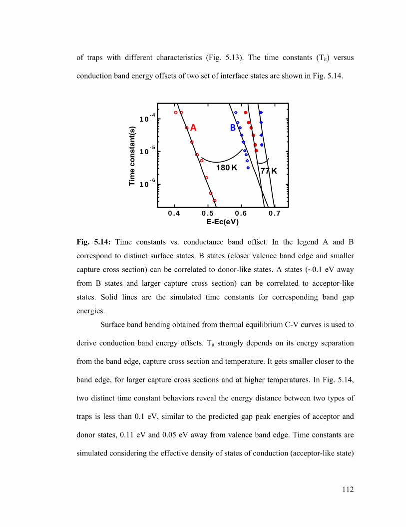
112
of traps with different characteristics (Fig. 5.13). The time constants (Tit) versus
conduction band energy offsets of two set of interface states are shown in Fig. 5.14.
Fig. 5.14: Time constants vs. conductance band offset. In the legend A and B
correspond to distinct surface states. B states (closer valence band edge and smaller
capture cross section) can be correlated to donor-like states. A states (~0.1 eV away
from B states and larger capture cross section) can be correlated to acceptor-like
states. Solid lines are the simulated time constants for corresponding band gap
energies.
Surface band bending obtained from thermal equilibrium C-V curves is used to
derive conduction band energy offsets. Tit strongly depends on its energy separation
from the band edge, capture cross section and temperature. It gets smaller closer to the
band edge, for larger capture cross sections and at higher temperatures. In Fig. 5.14,
two distinct time constant behaviors reveal the energy distance between two types of
traps is less than 0.1 eV, similar to the predicted gap peak energies of acceptor and
donor states, 0.11 eV and 0.05 eV away from valence band edge. Time constants are
simulated considering the effective density of states of conduction (acceptor-like state)
0.4 0.5 0.6 0.7
10-6
10-5
10-4
E-Ec(eV)
Tim
e co
nsta
nt(s
)
180 K 77 K
A B
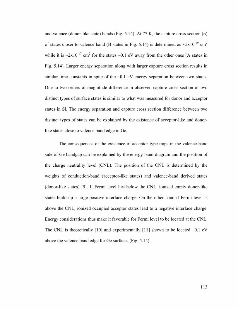
113
and valence (donor-like state) bands (Fig. 5.14). At 77 K, the capture cross section (σ)
of states closer to valence band (B states in Fig. 5.14) is determined as ~5x10-19 cm2
while it is ~2x10-17 cm2 for the states ~0.1 eV away from the other ones (A states in
Fig. 5.14). Larger energy separation along with larger capture cross section results in
similar time constants in spite of the ~0.1 eV energy separation between two states.
One to two orders of magnitude difference in observed capture cross section of two
distinct types of surface states is similar to what was measured for donor and acceptor
states in Si. The energy separation and capture cross section difference between two
distinct types of states can be explained by the existence of acceptor-like and donor-
like states close to valence band edge in Ge.
The consequences of the existence of acceptor type traps in the valence band
side of Ge bandgap can be explained by the energy-band diagram and the position of
the charge neutrality level (CNL). The position of the CNL is determined by the
weights of conduction-band (acceptor-like states) and valence-band derived states
(donor-like states) [9]. If Fermi level lies below the CNL, ionized empty donor-like
states build up a large positive interface charge. On the other hand if Fermi level is
above the CNL, ionized occupied acceptor states lead to a negative interface charge.
Energy considerations thus make it favorable for Fermi level to be located at the CNL.
The CNL is theoretically [10] and experimentally [11] shown to be located ~0.1 eV
above the valence band edge for Ge surfaces (Fig. 5.15).
114
Fig. 5.15: CNL level is located ~0.1eV from valence band edge. Grey region
corresponds to occupied traps. (a) Net charge built up at interface is close to zero for
Ge PMOS. (b) Negative charge builds up at interface for Ge NMOS, due to acceptor
type of traps below Fermi level. Acceptor traps consumes electrons from inversion
layer.
In PMOS inversion regime, Fermi level is located in the valence band side,
close to the CNL (Fig. 5.15 (a)). Hence, most of the acceptor traps above Fermi level
are empty and not ionized. Also, most of the donor traps are located below Fermi level
and not ionized. Therefore, net charge built up at interface is close to zero for Ge
PMOS inversion. However, in NMOS inversion regime, most of the acceptor states
are located below Fermi level and they are ionized. Occupied acceptor traps consume
electrons from the inversion layer (Fig. 5.15 (b)). Filling acceptor type traps results in
a net negative charge built up at interface that degrades NMOS inversion and causes
Coulomb scattering [13]. In summary, the acceptor type traps located in the valence
band side constitute a potential problem for NMOS but not for PMOS.
Dit distribution across Ge bandgap is determined using conductance
measurements performed at 77-250 K temperature range for GeO2/Ge and GeON/Ge
++++++ +
Ec
Ei
Ev
EFCNL
Acceptor (‐)
Donor (+)
E
z
PMOS Ec
Ei
EvEF
CNL
Acceptor (‐)
Donor (+)
E
z
‐‐‐‐‐‐ ‐‐
NMOS(a) (b)
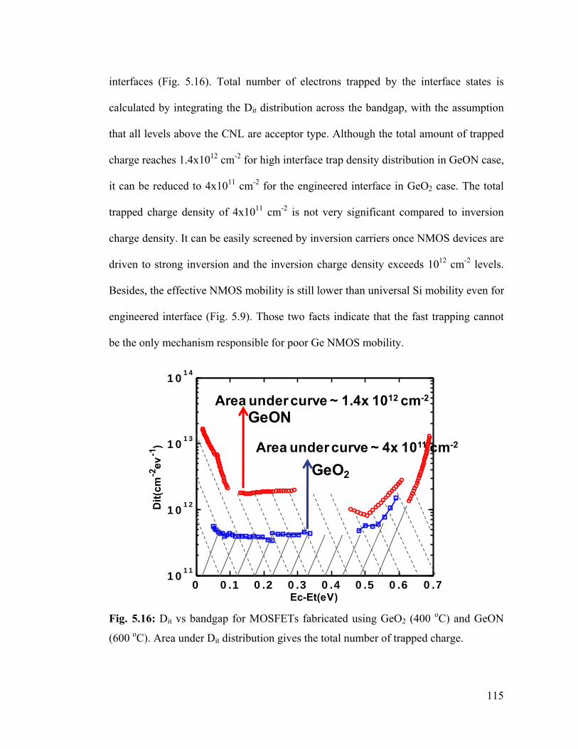
115
interfaces (Fig. 5.16). Total number of electrons trapped by the interface states is
calculated by integrating the Dit distribution across the bandgap, with the assumption
that all levels above the CNL are acceptor type. Although the total amount of trapped
charge reaches 1.4x1012 cm-2 for high interface trap density distribution in GeON case,
it can be reduced to 4x1011 cm-2 for the engineered interface in GeO2 case. The total
trapped charge density of 4x1011 cm-2 is not very significant compared to inversion
charge density. It can be easily screened by inversion carriers once NMOS devices are
driven to strong inversion and the inversion charge density exceeds 1012 cm-2 levels.
Besides, the effective NMOS mobility is still lower than universal Si mobility even for
engineered interface (Fig. 5.9). Those two facts indicate that the fast trapping cannot
be the only mechanism responsible for poor Ge NMOS mobility.
Fig. 5.16: Dit vs bandgap for MOSFETs fabricated using GeO2 (400 oC) and GeON
(600 oC). Area under Dit distribution gives the total number of trapped charge.
0 0.1 0.2 0.3 0.4 0.5 0.6 0.71011
1012
1013
1014
Ec-Et(eV)
Dit(
cm-2
ev-1
)
GeON
GeO2
Area under curve ~ 1.4x 1012 cm-2
Area under curve ~ 4x 1011 cm-2
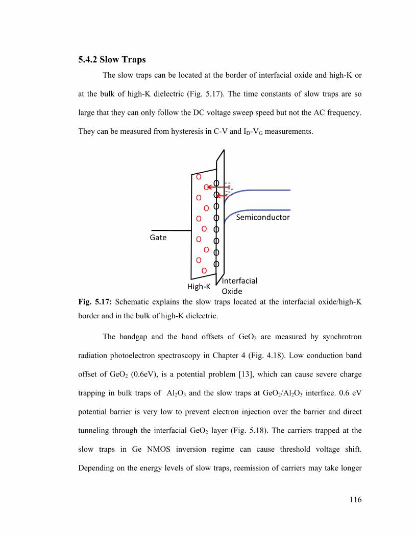
116
5.4.2 Slow Traps The slow traps can be located at the border of interfacial oxide and high-K or
at the bulk of high-K dielectric (Fig. 5.17). The time constants of slow traps are so
large that they can only follow the DC voltage sweep speed but not the AC frequency.
They can be measured from hysteresis in C-V and ID-VG measurements.
Fig. 5.17: Schematic explains the slow traps located at the interfacial oxide/high-K
border and in the bulk of high-K dielectric.
The bandgap and the band offsets of GeO2 are measured by synchrotron
radiation photoelectron spectroscopy in Chapter 4 (Fig. 4.18). Low conduction band
offset of GeO2 (0.6eV), is a potential problem [13], which can cause severe charge
trapping in bulk traps of Al2O3 and the slow traps at GeO2/Al2O3 interface. 0.6 eV
potential barrier is very low to prevent electron injection over the barrier and direct
tunneling through the interfacial GeO2 layer (Fig. 5.18). The carriers trapped at the
slow traps in Ge NMOS inversion regime can cause threshold voltage shift.
Depending on the energy levels of slow traps, reemission of carriers may take longer
Semiconductor
Interfacial OxideHigh‐K
OOOOOOOO
Gate
‐‐‐‐‐‐‐‐
OO
OO
OO
OO
OO
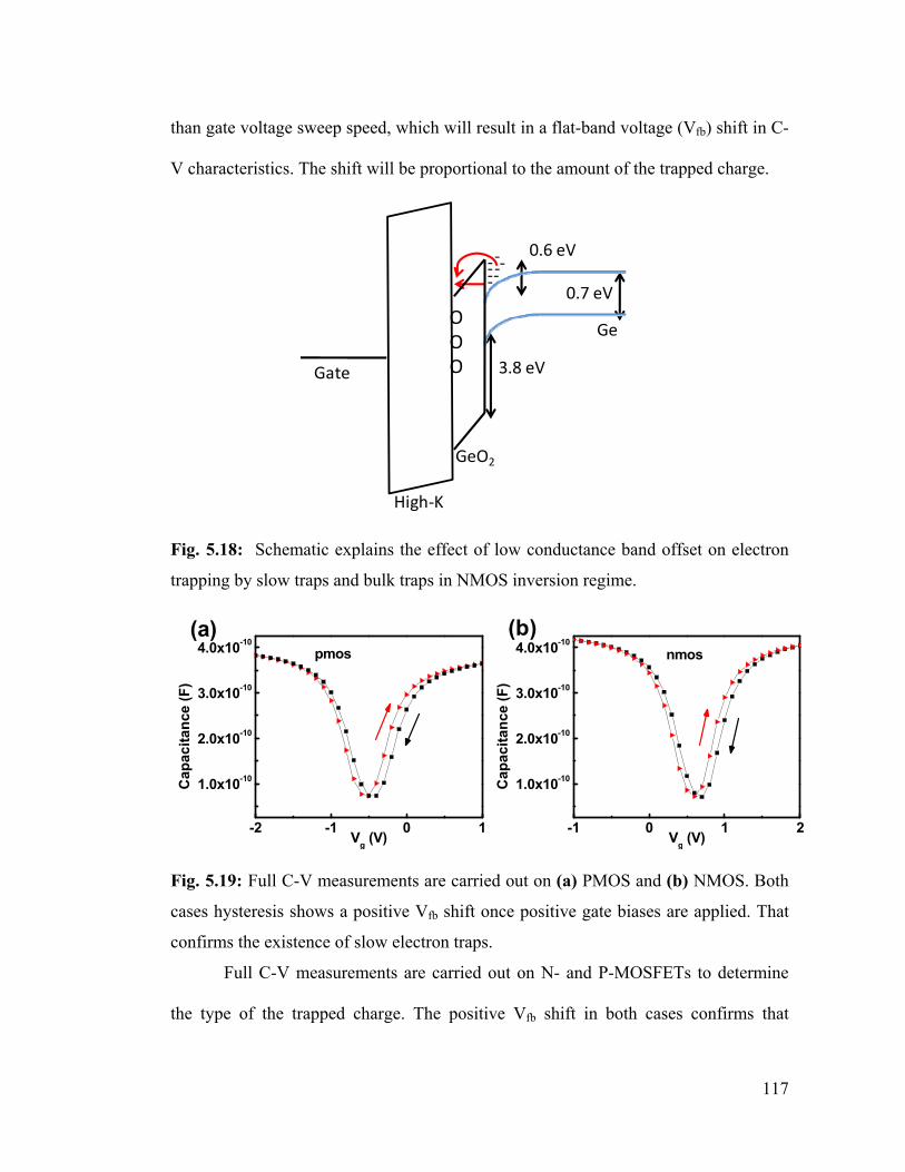
117
than gate voltage sweep speed, which will result in a flat-band voltage (Vfb) shift in C-
V characteristics. The shift will be proportional to the amount of the trapped charge.
Fig. 5.18: Schematic explains the effect of low conductance band offset on electron
trapping by slow traps and bulk traps in NMOS inversion regime.
Fig. 5.19: Full C-V measurements are carried out on (a) PMOS and (b) NMOS. Both
cases hysteresis shows a positive Vfb shift once positive gate biases are applied. That
confirms the existence of slow electron traps.
Full C-V measurements are carried out on N- and P-MOSFETs to determine
the type of the trapped charge. The positive Vfb shift in both cases confirms that
3.8 eV
0.6 eV
0.7 eV
Ge
GeO2
High‐K
OOOGate
‐‐‐‐‐‐ ‐‐
-2 -1 0 1
1.0x10⁻¹⁰
2.0x10⁻¹⁰
3.0x10⁻¹⁰
4.0x10⁻¹⁰
Cap
acita
nce
(F)
Vg (V)
pmos
-1 0 1 2
1.0x10⁻¹⁰
2.0x10⁻¹⁰
3.0x10⁻¹⁰
4.0x10⁻¹⁰
Cap
acita
nce
(F)
Vg (V)
nmos(a) (b)
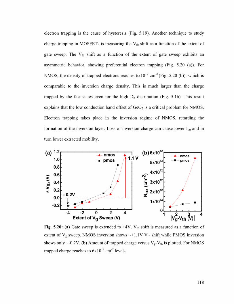
118
electron trapping is the cause of hysteresis (Fig. 5.19). Another technique to study
charge trapping in MOSFETs is measuring the Vfb shift as a function of the extent of
gate sweep. The Vfb shift as a function of the extent of gate sweep exhibits an
asymmetric behavior, showing preferential electron trapping (Fig. 5.20 (a)). For
NMOS, the density of trapped electrons reaches 6x1012 cm-2 (Fig. 5.20 (b)), which is
comparable to the inversion charge density. This is much larger than the charge
trapped by the fast states even for the high Dit distribution (Fig. 5.16). This result
explains that the low conduction band offset of GeO2 is a critical problem for NMOS.
Electron trapping takes place in the inversion regime of NMOS, retarding the
formation of the inversion layer. Loss of inversion charge can cause lower Ion and in
turn lower extracted mobility.
Fig. 5.20: (a) Gate sweep is extended to ±4V. Vfb shift is measured as a function of
extent of Vg sweep. NMOS inversion shows ~+1.1V Vfb shift while PMOS inversion
shows only ~-0.2V. (b) Amount of trapped charge versus Vg-Vth is plotted. For NMOS
trapped charge reaches to 6x1012 cm-2 levels.
-4 -2 0 2 4-0.20.00.20.40.60.81.01.2
- 0.2V
nmos pmos
Δ V
fb (V
)
Extent of Vg Sweep (V)
1.1 V
1 2 3 40
1x10¹²
2x10¹²
3x10¹²
4x10¹²
5x10¹²
6x10¹²
nmos pmos
N
ox (c
m-2
)
|Vg-Vth (V)|
(a) (b)
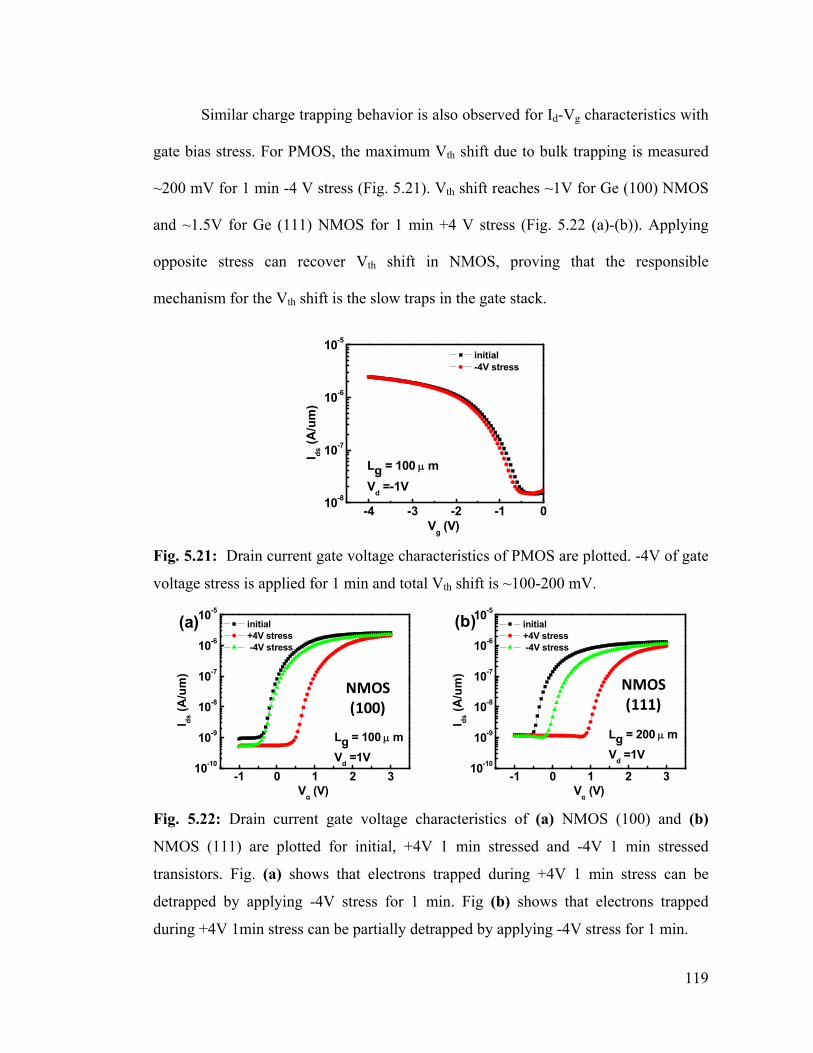
119
Similar charge trapping behavior is also observed for Id-Vg characteristics with
gate bias stress. For PMOS, the maximum Vth shift due to bulk trapping is measured
~200 mV for 1 min -4 V stress (Fig. 5.21). Vth shift reaches ~1V for Ge (100) NMOS
and ~1.5V for Ge (111) NMOS for 1 min +4 V stress (Fig. 5.22 (a)-(b)). Applying
opposite stress can recover Vth shift in NMOS, proving that the responsible
mechanism for the Vth shift is the slow traps in the gate stack.
Fig. 5.21: Drain current gate voltage characteristics of PMOS are plotted. -4V of gate
voltage stress is applied for 1 min and total Vth shift is ~100-200 mV.
Fig. 5.22: Drain current gate voltage characteristics of (a) NMOS (100) and (b)
NMOS (111) are plotted for initial, +4V 1 min stressed and -4V 1 min stressed
transistors. Fig. (a) shows that electrons trapped during +4V 1 min stress can be
detrapped by applying -4V stress for 1 min. Fig (b) shows that electrons trapped
during +4V 1min stress can be partially detrapped by applying -4V stress for 1 min.
-4 -3 -2 -1 010-8
10-7
10-6
10-5
initial -4V stress
I ds (A
/um
)
Vg (V)
Lg = 100 μ mVd =-1V
NMOS (100)
NMOS (111)
-1 0 1 2 310-10
10-9
10-8
10-7
10-6
10-5
initial +4V stress -4V stress
I ds (A
/um
)
Vg (V)
Lg = 100 μ mVd =1V
-1 0 1 2 310-10
10-9
10-8
10-7
10-6
10-5
initial +4V stress -4V stress
I ds (A
/um
)
Vg (V)
Lg = 200 μ mVd =1V
(a) (b)
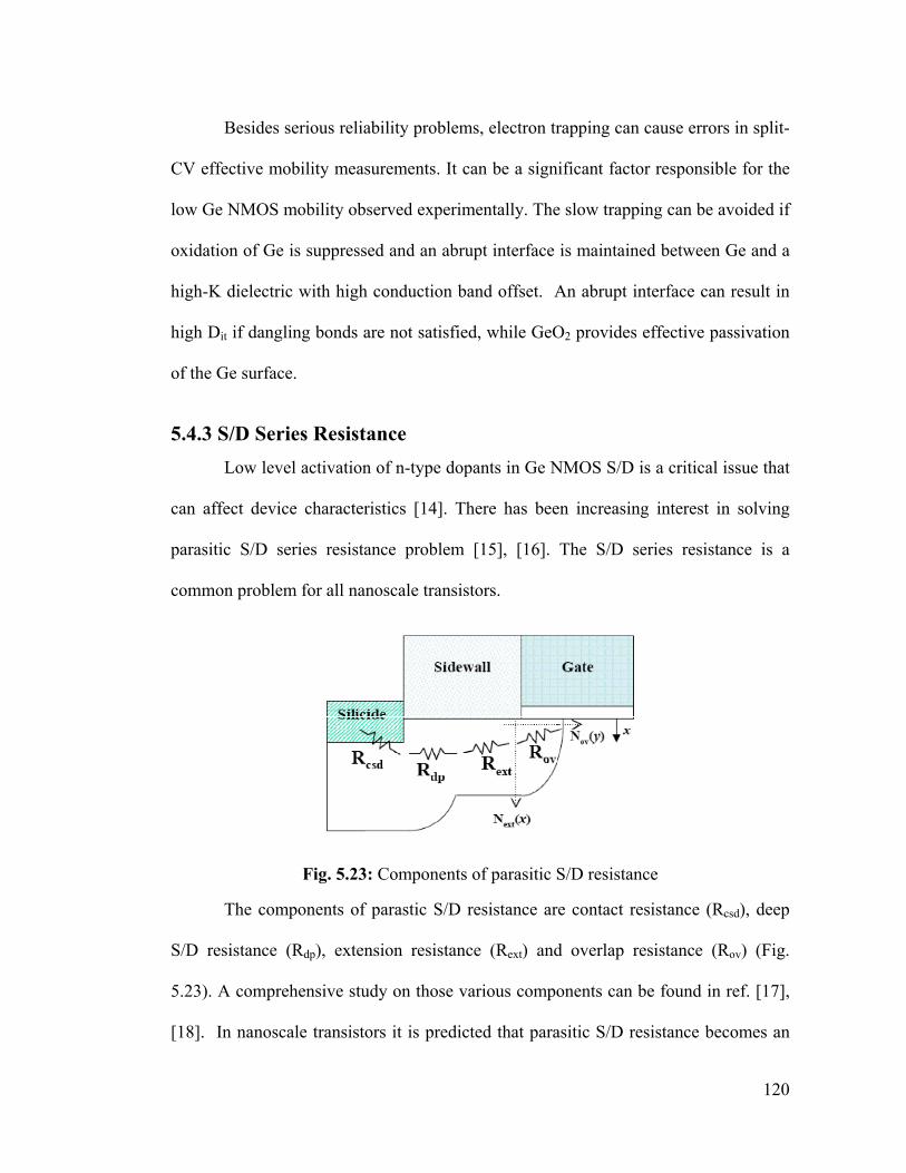
120
Besides serious reliability problems, electron trapping can cause errors in split-
CV effective mobility measurements. It can be a significant factor responsible for the
low Ge NMOS mobility observed experimentally. The slow trapping can be avoided if
oxidation of Ge is suppressed and an abrupt interface is maintained between Ge and a
high-K dielectric with high conduction band offset. An abrupt interface can result in
high Dit if dangling bonds are not satisfied, while GeO2 provides effective passivation
of the Ge surface.
5.4.3 S/D Series Resistance Low level activation of n-type dopants in Ge NMOS S/D is a critical issue that
can affect device characteristics [14]. There has been increasing interest in solving
parasitic S/D series resistance problem [15], [16]. The S/D series resistance is a
common problem for all nanoscale transistors.
Fig. 5.23: Components of parasitic S/D resistance
The components of parastic S/D resistance are contact resistance (Rcsd), deep
S/D resistance (Rdp), extension resistance (Rext) and overlap resistance (Rov) (Fig.
5.23). A comprehensive study on those various components can be found in ref. [17],
[18]. In nanoscale transistors it is predicted that parasitic S/D resistance becomes an
121
increasing fraction of the ON resistance of the transistor, hence posing a serious limit
to drive current enhancement as gate lengths are scaled. The effect of serious
resistance on drive current is included in the drain current expression in linear regime,
at a low drain voltage:
(5.1)
In split CV effective mobility measurements, the effective mobility expression:
(5.2)
where Qn is inversion carrier density, L is the channel length and W is the channel
width. The drain conductance, gD, is:
| ~ (5.3)
The voltage drop across parasitic S/D resistance, IDRSD, causes a reduction in
the drain current. Hence, measured mobility by split CV appears to be lower than it is
original value. In order to eliminate the S/D series resistance and to measure the
trapping free mobility, gated Hall devices are fabricated (Fig. 5.24). Additional
voltage contacts (shown with Vd in Fig. 5.24) of the gated Hall devices allow for
performing four-probe measurements of the transistor conductance, avoiding the effect
of the S/D series resistance on the mobility extraction. Some of the applied drain
voltage drops over the parasitic S/D resistance. However, the voltage drop across the
channel needs to be known to calculate effective mobility using equation (5.3). The
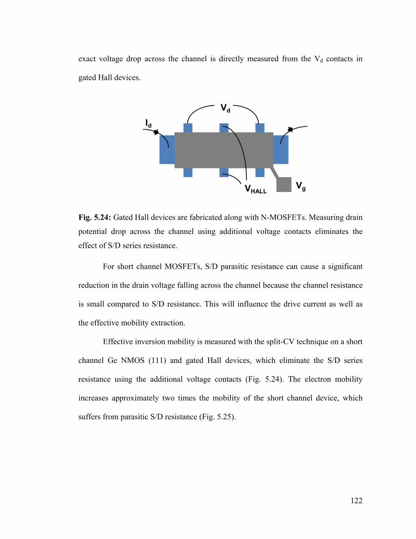
122
exact voltage drop across the channel is directly measured from the Vd contacts in
gated Hall devices.
Fig. 5.24: Gated Hall devices are fabricated along with N-MOSFETs. Measuring drain
potential drop across the channel using additional voltage contacts eliminates the
effect of S/D series resistance.
For short channel MOSFETs, S/D parasitic resistance can cause a significant
reduction in the drain voltage falling across the channel because the channel resistance
is small compared to S/D resistance. This will influence the drive current as well as
the effective mobility extraction.
Effective inversion mobility is measured with the split-CV technique on a short
channel Ge NMOS (111) and gated Hall devices, which eliminate the S/D series
resistance using the additional voltage contacts (Fig. 5.24). The electron mobility
increases approximately two times the mobility of the short channel device, which
suffers from parasitic S/D resistance (Fig. 5.25).
Vd
Vg
Id
VHALL
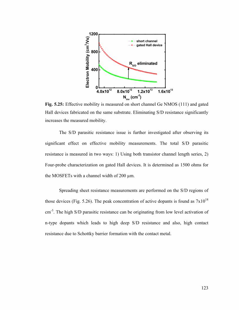
123
Fig. 5.25: Effective mobility is measured on short channel Ge NMOS (111) and gated
Hall devices fabricated on the same substrate. Eliminating S/D resistance significantly
increases the measured mobility.
The S/D parasitic resistance issue is further investigated after observing its
significant effect on effective mobility measurements. The total S/D parasitic
resistance is measured in two ways: 1) Using both transistor channel length series, 2)
Four-probe characterization on gated Hall devices. It is determined as 1500 ohms for
the MOSFETs with a channel width of 200 µm.
Spreading sheet resistance measurements are performed on the S/D regions of
those devices (Fig. 5.26). The peak concentration of active dopants is found as 7x10¹⁸
cm-3. The high S/D parasitic resistance can be originating from low level activation of
n-type dopants which leads to high deep S/D resistance and also, high contact
resistance due to Schottky barrier formation with the contact metal.
4.0x10¹² 8.0x10¹² 1.2x10¹³ 1.6x10130
400
800
1200
RS/D eliminated
short channel gated Hall device
Elec
tron
Mob
ility
(cm
2 /Vs)
Ninv (cm-2)
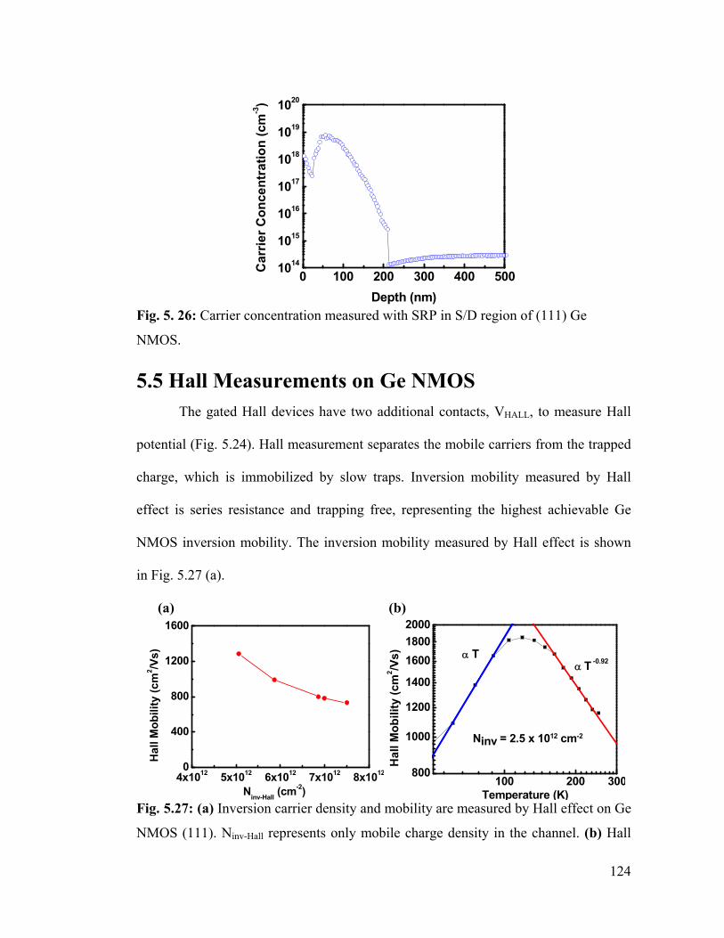
124
Fig. 5. 26: Carrier concentration measured with SRP in S/D region of (111) Ge
NMOS.
5.5 Hall Measurements on Ge NMOS The gated Hall devices have two additional contacts, VHALL, to measure Hall
potential (Fig. 5.24). Hall measurement separates the mobile carriers from the trapped
charge, which is immobilized by slow traps. Inversion mobility measured by Hall
effect is series resistance and trapping free, representing the highest achievable Ge
NMOS inversion mobility. The inversion mobility measured by Hall effect is shown
in Fig. 5.27 (a).
(a) (b)
Fig. 5.27: (a) Inversion carrier density and mobility are measured by Hall effect on Ge
NMOS (111). Ninv-Hall represents only mobile charge density in the channel. (b) Hall
0 100 200 300 400 5001014
1015
1016
1017
1018
1019
1020
Car
rier C
once
ntra
tion
(cm
-3)
Depth (nm)
4x10¹² 5x10¹² 6x10¹² 7x10¹² 8x10120
400
800
1200
1600
Ninv-Hall (cm-2)
Hal
l Mob
ility
(cm
2 /Vs)
100 200 300800
1000
1200
1400
160018002000
Hal
l Mob
ility
(cm
2 /Vs)
Temperature (K)
Ninv = 2.5 x 1012 cm-2
α Tα T -0.92
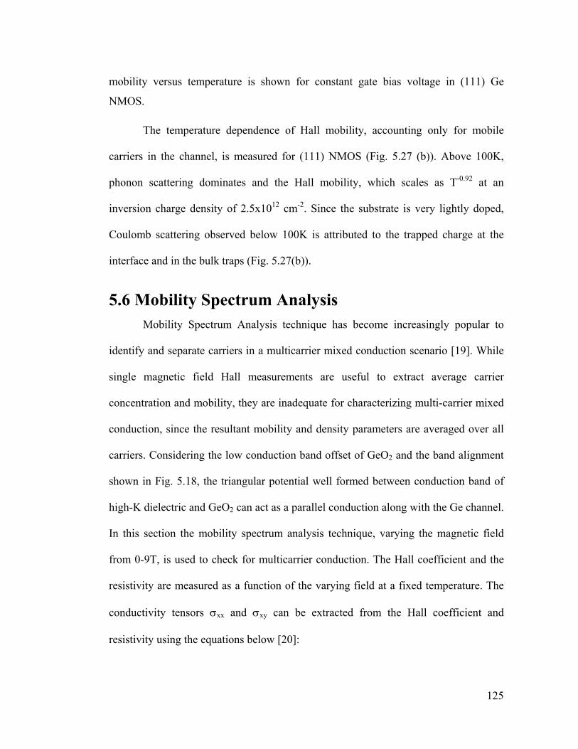
125
mobility versus temperature is shown for constant gate bias voltage in (111) Ge
NMOS.
The temperature dependence of Hall mobility, accounting only for mobile
carriers in the channel, is measured for (111) NMOS (Fig. 5.27 (b)). Above 100K,
phonon scattering dominates and the Hall mobility, which scales as T-0.92 at an
inversion charge density of 2.5x1012 cm-2. Since the substrate is very lightly doped,
Coulomb scattering observed below 100K is attributed to the trapped charge at the
interface and in the bulk traps (Fig. 5.27(b)).
5.6 Mobility Spectrum Analysis Mobility Spectrum Analysis technique has become increasingly popular to
identify and separate carriers in a multicarrier mixed conduction scenario [19]. While
single magnetic field Hall measurements are useful to extract average carrier
concentration and mobility, they are inadequate for characterizing multi-carrier mixed
conduction, since the resultant mobility and density parameters are averaged over all
carriers. Considering the low conduction band offset of GeO2 and the band alignment
shown in Fig. 5.18, the triangular potential well formed between conduction band of
high-K dielectric and GeO2 can act as a parallel conduction along with the Ge channel.
In this section the mobility spectrum analysis technique, varying the magnetic field
from 0-9T, is used to check for multicarrier conduction. The Hall coefficient and the
resistivity are measured as a function of the varying field at a fixed temperature. The
conductivity tensors σxx and σxy can be extracted from the Hall coefficient and
resistivity using the equations below [20]:
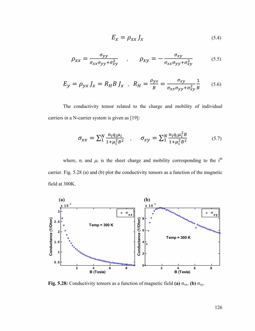
126
(5.4)
, (5.5)
, (5.6)
The conductivity tensor related to the charge and mobility of individual
carriers in a N-carrier system is given as [19]:
∑ , ∑ (5.7)
where, ni and μi is the sheet charge and mobility corresponding to the ith
carrier. Fig. 5.28 (a) and (b) plot the conductivity tensors as a function of the magnetic
field at 300K.
(a) (b)
Fig. 5.28: Conductivity tensors as a function of magnetic field (a) σxx. (b) σxy.
2 4 6 8
0.5
1
1.5
2
2.5
3
x 10-3
B (Tesla)
Con
duct
ance
(1/O
hm)
Temp = 300 K
σxx
2 4 6 80
2
4
6
8
x 10-5
B (Tesla)
Con
duct
ance
(1/O
hm)
Temp = 300 K
σxy
127
A least mean square fit algorithm is used to the fit the experimental data
assuming one, two and three types of carriers as per equation (5.7). Good fit with
experiment data is obtained assuming just one type of carrier. Hence, a parallel
conduction path in the potential well between GeO2 and high-K, along with the main
Ge channel is unlikely.
5.7 High Mobility Ge NMOS
Fig. 5.29 summarizes all the mechanisms and their contributions to effective
inversion mobility in Ge NMOS (111). The inversion charge density is measured with
split-CV technique and the mobility is extracted using equations (5.2) and (5.3).
1) The effective mobility measured on short channel Ge NMOS (green curve, w/
RS/D w/ Qtrapped) is lower than universal Si electron mobility, similar to what was
measured previously for Ge NMOS [21].
2) The gated Hall devices fabricated on the same substrate can eliminate the
effect of parasitic S/D resistance in the measurements, which significantly increases
the measured effective mobility. The electron mobility is found to be ~1.5 times the
universal Si mobility (RS/D free, red curve). To the best of our knowledge, this is the
highest Ge NMOS inversion mobility directly measured.
3) The trapped charge can be calculated using the Vfb shift in C-V measurements.
The RS/D free NMOS mobility can be corrected for the trapped charge as well. The
electron mobility is even higher, ~2 times the universal Si mobility (Qtrapped corrected,
blue curve), if the trapped charge is accounted for.
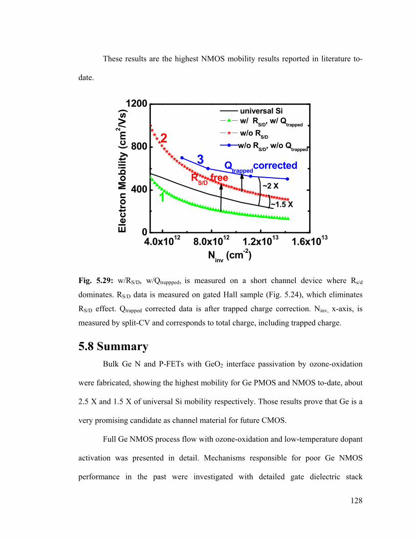
128
These results are the highest NMOS mobility results reported in literature to-
date.
Fig. 5.29: w/RS/D, w/Qtrappped, is measured on a short channel device where Rs/d
dominates. RS/D data is measured on gated Hall sample (Fig. 5.24), which eliminates
RS/D effect. Qtrapped corrected data is after trapped charge correction. Ninv, x-axis, is
measured by split-CV and corresponds to total charge, including trapped charge.
5.8 Summary Bulk Ge N and P-FETs with GeO2 interface passivation by ozone-oxidation
were fabricated, showing the highest mobility for Ge PMOS and NMOS to-date, about
2.5 X and 1.5 X of universal Si mobility respectively. Those results prove that Ge is a
very promising candidate as channel material for future CMOS.
Full Ge NMOS process flow with ozone-oxidation and low-temperature dopant
activation was presented in detail. Mechanisms responsible for poor Ge NMOS
performance in the past were investigated with detailed gate dielectric stack
4.0x10¹² 8.0x10¹² 1.2x10¹³ 1.6x10130
400
800
1200
1
32
~2 XRS/D free
universal Si w/ RS/D, w/ Qtrapped
w/o RS/D
w/o RS/D, w/o Qtrapped
Elec
tron
Mob
ility
(cm
2 /Vs)
Ninv (cm-2)
Qtrappedcorrected
~1.5 X
129
characterizations and Hall mobility analyses for the first time. The acceptor type traps
located in the valence band side of Ge bandgap were directly measured using
conductance technique and trap time constant measurements. High S/D parasitic
resistance, inversion charge loss due to trapping, and high interface trap density were
identified as the mechanisms responsible for Ge NMOS performance degradation. To
further improve the NMOS performance, reduction in S/D parasitic resistance and
improvement in gate dielectric stack are required. These findings are potentially
important for better understanding of Ge-based transistors for future CMOS
applications.
5.9 References [1] J. Mitard ,B.De Jaeger, F. E. Leys, G. Hellings, K. Martens, G. Eneman, D. P. Brunco, R.
Loo, J. C. Lin, D. Shamiryan, T. Vandeweyer, G. Winderickx, E. Vrancken, C. H. Yu, K.
De Meyer, M. Caymax, L. Pantisano, M. Meuris, M Heyns, M. Mitard, “Record
ION/IOFF performance for 65nm Ge pMOSFET and novel Si passivation scheme
for improved EOT scalability”, IEDM Tech. Dig., pp.873, 2008.
[2] D. Kuzum, A. J. Pethe , T. Krishnamohan, Y. Oshima, Y. Sun, J. P. McVittie, P.
A. Pianetta, P. C. McIntyre, K. C. Saraswat, “Interface-engineered Ge (100) and
(111), N- and P-FETs with high mobility” , IEDM Tech. Dig., pp. 723, 2007.
[3] D. S. Yu, C. H. Huang, A. Chin, C. Zhu, M. F. Li, B. J. Cho, D.-L. Kwong,
“Al2O3-Ge-On-Insulator n- and p-MOSFETs with fully NiSi and NiGe dual gates”,
Elec. Dev. Lett., 25, pp. 138-140, 2004.
[4] S. J. Whang, S. J. Lee, F. Gao, N. Wu, C. X. Zhu, J. S. Pan, L. J. Tang, D. L.
Kwong, “Germanium p- & n-MOSFETs fabricated with novel surface passivation
130
(plasma-PH3 and thin AlN) and TaN/HfO2 gate stack”, IEDM Tech. Dig., pp. 307,
2004.
[5] H. Shang, K-L. Lee, P. Kozlowski, C. D’emic, I. Babich, E. Sikorski, M. Ieong,
H.-S. P. Wong, K. Guarini, W. Haensch, “Self-aligned n-channel germanium
MOSFETs with a thin Geoxynitride gate dielectric and tungsten gate”, IEEE Elec.
Dev. Lett., vol.25, pp.135-138, 2004.
[6] W. P. Bai, N. Lu, A. Ritenour, M. L. Lee, D. A. Antoniadis, D.-L. Kwong, “Ge n-
MOSFET on lightly doped substrates with High-K dielectric and TaN gate”, Elec.
Dev. Lett., 27, pp. 175-177, 2006.
[7] D. Kuzum, T. Krishnamohan, A. J. Pethe , A. K. Okyay, Y. Oshima, Y. Sun, J. P.
McVittie, P. A. Pianetta, P. C. McIntyre, K. C. Saraswat, “Ge interface
engineering with ozone-oxidation for low interface state density”, Elec. Dev. Lett.,
29, pp. 328-330, 2008.
[8] E. H. Nicollian and J. R. Brews, MOS Physics and Technology. Wiley, New York,
2003.
[9] H. Luth, Solid Surfaces, Interfaces and Thin Films, Springer, New York, 2001.
[10] P. Broqvist, A. Alkauskas, A. Pasquarello, “Defect levels of dangling bonds in
silicon and germanium through hybrid functional”, Phys. Rev. B.,78,075203, 2008.
[11] A. Dimoulas, P. Tsipas, A. Sotiropoulos, E. K. Evangelou, “Fermi-level
pinning and charge neutrality level in germanium”, Appl. Phys. Lett, 89, 252110,
2006.
[12] P. Tsipas, A. Dimolulas, “Modeling of negatively charged states at the Ge
surface and interfaces”, Appl. Phys. Lett, 94, 012114, 2009.
131
[13] G. Lucovsky, S. Lee, J. P. Long, H. Seo, J. Luning, “Elimination of GeO2 and
Ge3N4 interfacial transition regions and defects at n-type Ge interfaces: A pathway
for formation of n-MOS devices on Ge substrates”, Appl. Surf. Sci., vol. 254, pp.
7933, 2008.
[14] C. O. Chui, L. Kulig, J. Moran, W. Tsai, K. C. Saraswat, “Germanium n-type
shallow junction dependences”, Appl. Phys. Lett, 87, 091909, 2005.
[15] M. Kobayashi, A. Kinoshita, K. Saraswat, H-S P Wong and Y. Nishi, “Fermi
Level Depinning in Metal/Ge Schottky Junction for Metal Source/Drain Ge Metal-
Oxide-Semiconductor Field Effect Transistor Applications”, J. Appl. Phys., 105,
023702, 2009.
[16] J. H. Park, M. Tada, D. Kuzum, P. Kapur, H.-Y. Yu, H.-S.P. Wong, K. C.
Saraswat, “Low Temperature (=380°C) and High Performance Ge CMOS with
Novel Source/Drain by Metal-Induced Dopants Activation and High-K/Metal Gate
Stack for Monolithic 3D Integration”, IEDM Tech. Dig., pp. 389, 2008.
[17] S-D. Kim, C.-M. Park and J. C. S. Woo, “Advanced model and analysis of
series resistance for CMOS scaling into nanometer regime – Part I: Theoretical
derivation”, IEEE Trans. Elec. Dev., Vol. 49, No. 3, pp. 457-466, March 2002.
[18] S-D. Kim, C.-M. Park and J. C. S. Woo, “Advanced model and analysis of
series resistance for CMOS scaling into nanometer regime – Part II: Quantitative
analysis”, IEEE Trans. on Elect. Dev., vol. 49, pp. 467-472, March 2002.
[19] G. Du, J. R. Lindemuth, B. C. Dodrill, R. Sandhu, M. Wojtowicz, M. S.
Goorsky, I. Vurgaftman, J. R. Meyer, “Characterizing Multi-Carrier Devices with
132
Quantitative Mobility Spectrum Analysis and Variable Field Hall Measurements”,
Jpn. J. Appl. Phys., 41, pp.1055, 2002.
[20] N. Miura, Physics of Semiconductors in High Magnetic Fields, Oxford
University Press, 2008.
[21] D. Kuzum, A. J. Pethe, T. Krishnamohan, K. C. Saraswat, “Ge (100) and (111)
N- and P-FETs with High Mobility and Low-T Mobility Characterization”, IEEE
Trans. Elec. Dev., vol. 56, pp.648-655, 2009.

133
134
Chapter 6 Conclusions and Future Directions
6.1 Introduction Drive current saturation is fundamentally limiting the future scaling of CMOS
technology. The carrier injection velocity from the source into the channel and the
high density of states are accepted as the main factors affecting the drive current in
nanoscale ballistic transistors. High mobility channel materials should be incorporated
to overcome the scaling bottleneck and allow further improvements in transistor
performance. Ge is a strong candidate as a channel material, owing to its high bulk
hole and electron mobilities and high density of states in both conduction and valence
bands. It also has the advantage of process compatibility and easy integration with the
state-of-art Si CMOS technology. However, there are a few critical issues to be solved
in device level before integration of Ge to Si CMOS:
1) Ge does not have a stable native insulator, as Si has. A high quality interface
and gate dielectric stack should be developed for Ge.
135
2) The low solid solubility and high diffusivity of n-type dopants in Ge make the
source/drain formation challenging. A source/drain technology providing low
parasitic resistance should be developed.
3) In spite of the successful experimental demonstrations for Ge PMOS, Ge
NMOS have exhibited low drive currents and poor mobility by several
demonstrations worldwide. Performance improvement in Ge NMOS is
mandatory.
This dissertation focuses on the first and third challenges. It investigates them
in detail and proposes solutions to move one step ahead in realizing Ge MOSFETs
for future high performance CMOS applications.
6.2 Dissertation Summary Bulk Ge N and P-FETs were fabricated with GeOxNy passivation, which was
developed in Saraswat Research Group previously. They exhibited the highest
inversion electron mobility reported to-date and ~2X improvement over Si universal
hole mobility. The effect of surface orientation on electron and hole mobilities and
interface trap density was investigated on Ge MOSFETs. A 50% higher electron
mobility was demonstrated for the (111) surface orientation compared to (100) for Ge
NMOS. The carrier scattering mechanisms were studied through low temperature
mobility measurements. Charge trapping and Coulomb scattering were found to be
primarily responsible for the poor Ge NMOS mobility. The Dit distribution across the
Ge bandgap and close to the band edges was measured. Higher trap densities near the
conduction band edge of (100) Ge was observed, whereas, the (111) substrate
exhibited a more symmetric Dit distribution. These findings changed the research
136
directions towards a more careful characterization of Ge interface and the
development of a technique to engineer Ge interface and to obtain a high quality gate
dielectric stack.
All the interface characterization techniques and interface trap distribution
measurements in literature were examined carefully to find a proper method to
characterize Ge interface. Nicollian-Goetzberger conductance technique was applied
on Ge devices at low temperatures (77 K-250 K). It was demonstrated that low
temperature conductance measurements give an accurate relative comparison for
samples with different qualities of interface passivation. The conventional room
temperature characterization techniques were shown to give inaccurate results for Ge
due to the effect of thermal generation and weak inversion responses. Measurable
window of the bandgap at each temperature range was calculated using interface trap
time constants. The effect of series resistance on conductance measurements was
clarified and the misleading Dit extractions were pointed.
A new technique to electrically passivate and engineer the Ge interface using
thermal oxidation in ozone prior to a dielectric deposition was developed to improve
CMOS performance. Dit distributions over the bandgap and close to band edges were
extracted using conductance technique at low temperatures. A minimum Dit of 3x10¹¹
cm-2 V-1 was obtained for samples oxidized at 400 °C in ozone ambient, which is in
the range of state-of-the-art Si/High-K dielectric interface quality. Ozone-oxidation
process was characterized in detail. Lower or higher oxidation temperatures than
400°C showed increase in Dit values due to formation of Ge suboxide (GeOx) states.
Physical quality of the interface was investigated through Ge 3d spectra
137
measurements. It was shown that the interface trap density is strongly affected by the
distribution of oxidation states and quality of the suboxide layer.
Following the development of engineered Ge interface, bulk Ge N and P-FETs
were fabricated using ozone-oxidation. They exhibited the highest mobility for Ge
PMOS and NMOS to-date, about 2.5 X and 1.5 X of universal Si mobility
respectively. Those results have proven that Ge is a very promising candidate as
channel material for future CMOS.
The mechanisms responsible for poor Ge NMOS performance in the past were
investigated by detailed gate dielectric stack characterizations and Hall mobility
analyses for the first time. The acceptor type traps located in the valence band side of
Ge bandgap were directly measured using the conductance technique and the trap time
constant measurements. High S/D parasitic resistance, inversion charge loss due to
trapping, and high interface trap density were identified as the mechanisms
responsible for the Ge NMOS performance degradation. These findings are potentially
important for better understanding of Ge-based transistors for future CMOS
applications.
138
6.3 Contributions and Impact of This Work • For the first time, the effect of surface orientation on Ge mobility is
investigated experimentally.
• Carrier scattering mechanisms are studied through low-T mobility
measurements to identify Ge NMOS performance problem.
• Low-temperature conductance technique is developed to examine Ge interface
and extract full distribution of Dit across Ge bandgap.
• Ozone-oxidation is introduced to engineer Ge/dielectric interface.
• Gate stack engineered with ozone-oxidation is integrated with low-temperature
S/D activation to fabricate Ge NMOS.
• Poor NMOS performance is investigated with fast and slow trap
characterizations and Hall mobility analyses for the first time.
• For the first time, the existence of acceptor traps in the valence band side and
the location of CNL close to valence band edge are shown by interface trap
time constant measurements.
• S/D series resistance and electron trapping are found to be the mechanisms
responsible for poor Ge NMOS in the past.
• Highest mobility for Ge NMOS to-date, about 1.5 X of universal Si mobility,
is reported.
139
6.4 Future Research Directions o To further improve the Ge NMOS performance, reduction in S/D parasitic
resistance is required. Conventional dopant activation techniques cannot
provide higher active dopant concentrations than 5x1019 cm-3. Pulsed laser
annealing techniques may be utilized to go above solid solubility limit.
o Alternatively, Schottky source/drain contacts can be considered for Ge NMOS.
Metal source/drain technologies with Fermi level unpinning may be
investigated.
o Another approach to improve the Ge NMOS performance is changing the
source/drain material with Si or SiGe, which will also bring the benefit of
tensile strain to Ge NMOS channel in addition to the increase in solid
solubility limit.
o The interface engineering techniques may be integrated to a Ge heterestructure
FET (Ge quantum well, GeO2/thin Ge/Si). The performance improvement and
strain effects may be investigated for Ge heterostructure P-FET.
o Improvement in gate dielectric stack, especially to avoid slow trapping, can be
achieved by an abrupt interface between Ge and a high-K dielectric with high
conduction band offset. An abrupt interface can result in high Dit. Therefore,
extra dangling bond passivation techniques (post deposition treatments) need
to be developed if this approach is followed.
o Non-planar device architectures, such as Ge MuGFETs can be a strong
direction of research for sub-20nm CMOS, taking the advantage of quantum
confinement and superior electrostatic control.
140
o Ge nanowire surround-gate FETs with Si or SiGe shells can combine the high
mobility transport with the superior electrostatic control. Ge nanowire devices
can be fabricated by a top-down approach, utilizing Ge condensation
technique.


![P087 Reliability Modeling on 90 nm n-channel MOSFETs with ...€¦ · [6] E. Maricau and G. Gielen,Analog IC Reliability in Nanometer CMOS,Springer Science Business Media New](https://static.fdocuments.in/doc/165x107/5fb67b16ce590245f2046e91/p087-reliability-modeling-on-90-nm-n-channel-mosfets-with-6-e-maricau-and.jpg)