Interconnection Reliability of HDI Printed Wiring Boards · Interconnection Reliability of HDI...
38
S07-3-1 Interconnection Reliability of HDI Printed Wiring Boards Tatsuo Suzuki Nec Toppan Circuit Solutions, Inc Shibata−city, Niigata−prefecture, Japan Abstract It is effective to use the stack-via-holes method (via-on-via structure), which stacks micro via-holes (MVH), in the development of higher density circuits on build-up printed wiring boards. When micro via-holes are repeatedly stacked, via holes cause an open circuit due to the difference in the thermal expansion of the copper and the glass epoxy base material. In order to verify the reliability of the stack-via-hole connection, we produced a range of test boards with differing numbers of stack-via-hole layers, material types (FR-4, high-Tg FR-4, low thermal expansion material, etc.), and via hole diameters (0.100 mm and 0.075 mm diameters). The boards were examined through DC current induced thermal cycling tests to determine the reliability of the various samples. In respect to the anti-migration properties, we also undertook research on pitches and base material types of micro via- holes. As a result of the evaluation, it was verified that the MVH, then interstitial-via-hole (IVH), followed by the plated through- hole (PTH) achieved the best connection reliability. As for base materials, it is recommended to use a high-Tg material with low thermal expansion qualities. We believe that an MVH diameter of 0.100 mm is preferable to prevent any void attributed from a high aspect ratio. No problem with the insulation reliability was found on any base material as long as the MVH pitch is 0.35 mm or more (or 0.25 mm between the hole walls). Introduction Due to higher pin counts and narrower pitches, much higher-density printed wiring boards are required. As a result, the adoption of ‘build-up printed wiring boards’ has spread, particularly in the area of communication station infrastructure, which requires a high level of reliability, and industrial devices such as IC testers. The method used for manufacturing build-up printed wiring boards generally employs the prepreg process to produce the build-up material and copper plating to ensure electrical connection. In the case of the filled via hole specification that fills MVH with copper, excellent reliability in electrical connection of MVH can be obtained. Moreover, an advantage of adopting the filled via holes is the via-on-via structure (stack-via-hole). This structure, in which filled via holes are stacked, enables more flexibility in the design of circuits, and can achieve much denser circuits. In our research of the connection reliability in relation to base materials, the number of build-up layers, and MVH diameters, certain design rules are needed to be established to ensure the reliability of the test results. As a comparative study, we also conducted further research on PTH and IVH. We will therefore confirm the connection reliability of the entire range of build-up printed wiring boards. It is becoming necessary to make MVH pitches even narrower in line with the progress of narrower pitches on surface mounting components. In this light, we decided to evaluate the insulation reliability by using test patterns on which pitches between MVH and MVH are gradually changed. The following sections will explain our method of manufacturing build-up printed wiring boards with copper-plated filled via holes, followed by the results of our evaluation of their connection reliability and insulation reliability. Manufacturing Method The manufacturing method used for the evaluation is shown in Figure 1. As for IVH, epoxy resin was filled in IVH after plating and a build-up layer formed by applying a thermal press on the prepreg material and copper foil after the formation of circuits. We used a CO 2 laser to make the holes for MVH. Since it is generally difficult to fabricate copper foil using a CO 2 laser, we made partial etchings on the copper foil prior to opening the holes with the laser. After plating the filled via holes, we formed a circuit pattern on both sides, and then applied a lamination layer, onto which we formed another circuit pattern to achieve three build-up layers. Stack-via-holes were produced by repeating this MVH formation as required. Presented in the ECWC 10 Conference at IPC Printed Circuits Expo®, SMEMA Council APEX® and Designers Summit 05
Transcript of Interconnection Reliability of HDI Printed Wiring Boards · Interconnection Reliability of HDI...

S07-3-1
Interconnection Reliability of HDI Printed Wiring Boards
Tatsuo Suzuki Nec Toppan Circuit Solutions, Inc
Shibata−city, Niigata−prefecture, Japan
Abstract It is effective to use the stack-via-holes method (via-on-via structure), which stacks micro via-holes (MVH), in the development of higher density circuits on build-up printed wiring boards. When micro via-holes are repeatedly stacked, via holes cause an open circuit due to the difference in the thermal expansion of the copper and the glass epoxy base material. In order to verify the reliability of the stack-via-hole connection, we produced a range of test boards with differing numbers of stack-via-hole layers, material types (FR-4, high-Tg FR-4, low thermal expansion material, etc.), and via hole diameters (0.100 mm and 0.075 mm diameters). The boards were examined through DC current induced thermal cycling tests to determine the reliability of the various samples. In respect to the anti-migration properties, we also undertook research on pitches and base material types of micro via- holes. As a result of the evaluation, it was verified that the MVH, then interstitial-via-hole (IVH), followed by the plated through-hole (PTH) achieved the best connection reliability. As for base materials, it is recommended to use a high-Tg material with low thermal expansion qualities. We believe that an MVH diameter of 0.100 mm is preferable to prevent any void attributed from a high aspect ratio. No problem with the insulation reliability was found on any base material as long as the MVH pitch is 0.35 mm or more (or 0.25 mm between the hole walls). Introduction Due to higher pin counts and narrower pitches, much higher-density printed wiring boards are required. As a result, the adoption of ‘build-up printed wiring boards’ has spread, particularly in the area of communication station infrastructure, which requires a high level of reliability, and industrial devices such as IC testers. The method used for manufacturing build-up printed wiring boards generally employs the prepreg process to produce the build-up material and copper plating to ensure electrical connection. In the case of the filled via hole specification that fills MVH with copper, excellent reliability in electrical connection of MVH can be obtained. Moreover, an advantage of adopting the filled via holes is the via-on-via structure (stack-via-hole). This structure, in which filled via holes are stacked, enables more flexibility in the design of circuits, and can achieve much denser circuits. In our research of the connection reliability in relation to base materials, the number of build-up layers, and MVH diameters, certain design rules are needed to be established to ensure the reliability of the test results. As a comparative study, we also conducted further research on PTH and IVH. We will therefore confirm the connection reliability of the entire range of build-up printed wiring boards. It is becoming necessary to make MVH pitches even narrower in line with the progress of narrower pitches on surface mounting components. In this light, we decided to evaluate the insulation reliability by using test patterns on which pitches between MVH and MVH are gradually changed. The following sections will explain our method of manufacturing build-up printed wiring boards with copper-plated filled via holes, followed by the results of our evaluation of their connection reliability and insulation reliability. Manufacturing Method The manufacturing method used for the evaluation is shown in Figure 1. As for IVH, epoxy resin was filled in IVH after plating and a build-up layer formed by applying a thermal press on the prepreg material and copper foil after the formation of circuits. We used a CO2 laser to make the holes for MVH. Since it is generally difficult to fabricate copper foil using a CO2 laser, we made partial etchings on the copper foil prior to opening the holes with the laser. After plating the filled via holes, we formed a circuit pattern on both sides, and then applied a lamination layer, onto which we formed another circuit pattern to achieve three build-up layers. Stack-via-holes were produced by repeating this MVH formation as required.
Presented in the ECWC 10 Conference at IPC Printed Circuits Expo®, SMEMA Council APEX® and
Designers Summit 05

S07-3-2
Figure 1 – Manufacturing Process
Body Connection Reliability One cause of long-term failure that may occur in printed wiring boards is an open circuit resulting from a crack of PTH. When thermal stress is imposed on a printed wiring board repeatedly, the difference in thermal expansion between the copper plate and the base material cause distortion of the board, creating an open circuit as a crack in the copper plate is formed. We must therefore pay attention to the failure mode for similar mechanisms on stack-via-holes as well. In order to determine any influence by the difference in thermal expansion between the materials, besides FR-4, we selected base materials with low thermal expansion specifications. Table 1 shows the specification values of base materials. For the evaluation we used 16 layer boards with a total board thickness of 2.0 mm and consisting of three build-up layers on each side of 10 layer IVH. The board thickness of the IVH layer (layers 4 - 13) was 1.3 mm, while the thickness between the build-up layers was 0.06 mm per layer.

S07-3-3
Table 1 – Characteristic Values of Materials
Evaluation method:
DC Current Induced Thermal Cycling Test (IPC-TM-650: 2.6.26).1 Three minutes of heating is followed by two minutes cooling. (max.150 degrees Celsius)
Pre-treatment: Ambient to 230 degrees Celsius in 3x3 cycles
The number of cycles: 2,000 cycles
Criterion: Change in conductive resistance 10%
Sample size: n = 6 Test pattern:
Daisy chain pattern for PTH, IVH & MVH
The design rules are shown in Table 2.
Table 2 – Design Rules
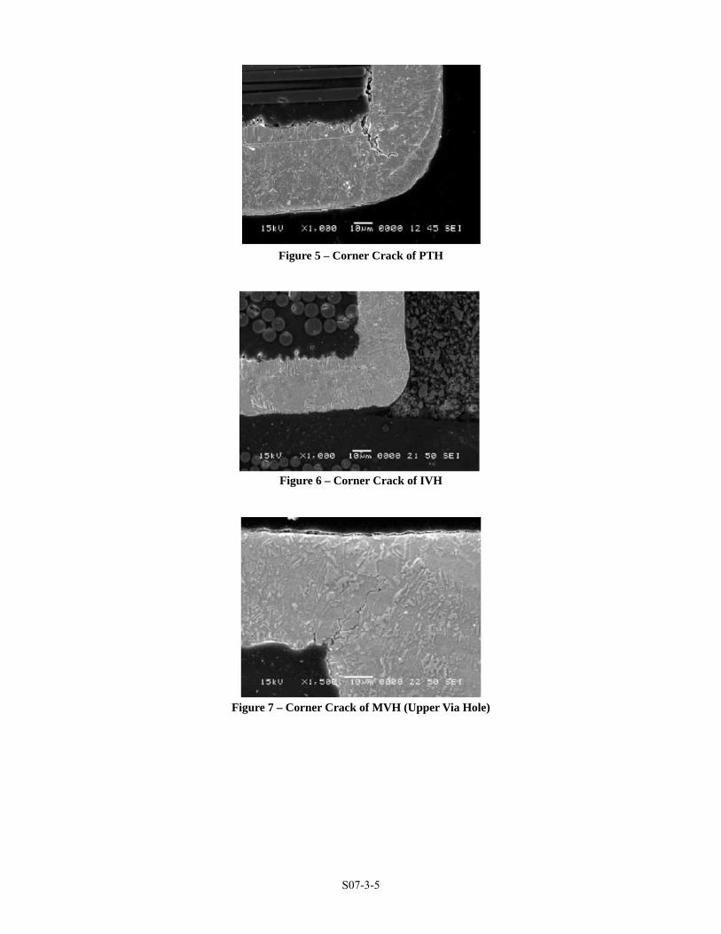
The MTTF (mean time to failure) results obtained for each base material type from the evaluation are shown in Table 3. Failures happened in order of PTH, IVH and MVH. The failure results caused in PTH, IVH and MVH (three-step stack) of the base material (a) are plotted on the Weibull Probability Paper and are shown in Figure 2. Upon comparing the results for various base material types, we confirm that the combination of high-Tg material with low thermal expansion specifications does not cause more failures than using FR-4 material. Furthermore, in the stack-via-hole area, it is assumed that cracks tend to be caused from the increase in distortion resulting from the difference in thermal expansion between the base material and copper when the number of build-up steps increases. When we checked the failure modes, barrel cracks and corner cracks were detected on PTH and IVH (see the Figures 3 - 6). In the case failure on MVH, corner cracks of MVH were also detected (see the Figures 7 and 8).

S07-3-4
Table 3 – MTTF
Figure 2 – Weibull Probability paper (Base Material (a) by Via Hole Types
Figure 3 – Barrel Crack of PTH
Figure 4 – Barrel Crack of IVH
S07-3-5
Figure 5 – Corner Crack of PTH
Figure 6 – Corner Crack of IVH
Figure 7 – Corner Crack of MVH (Upper Via Hole)

S07-3-6
Figure 8 – Corner Crack (Lower Via Hole)
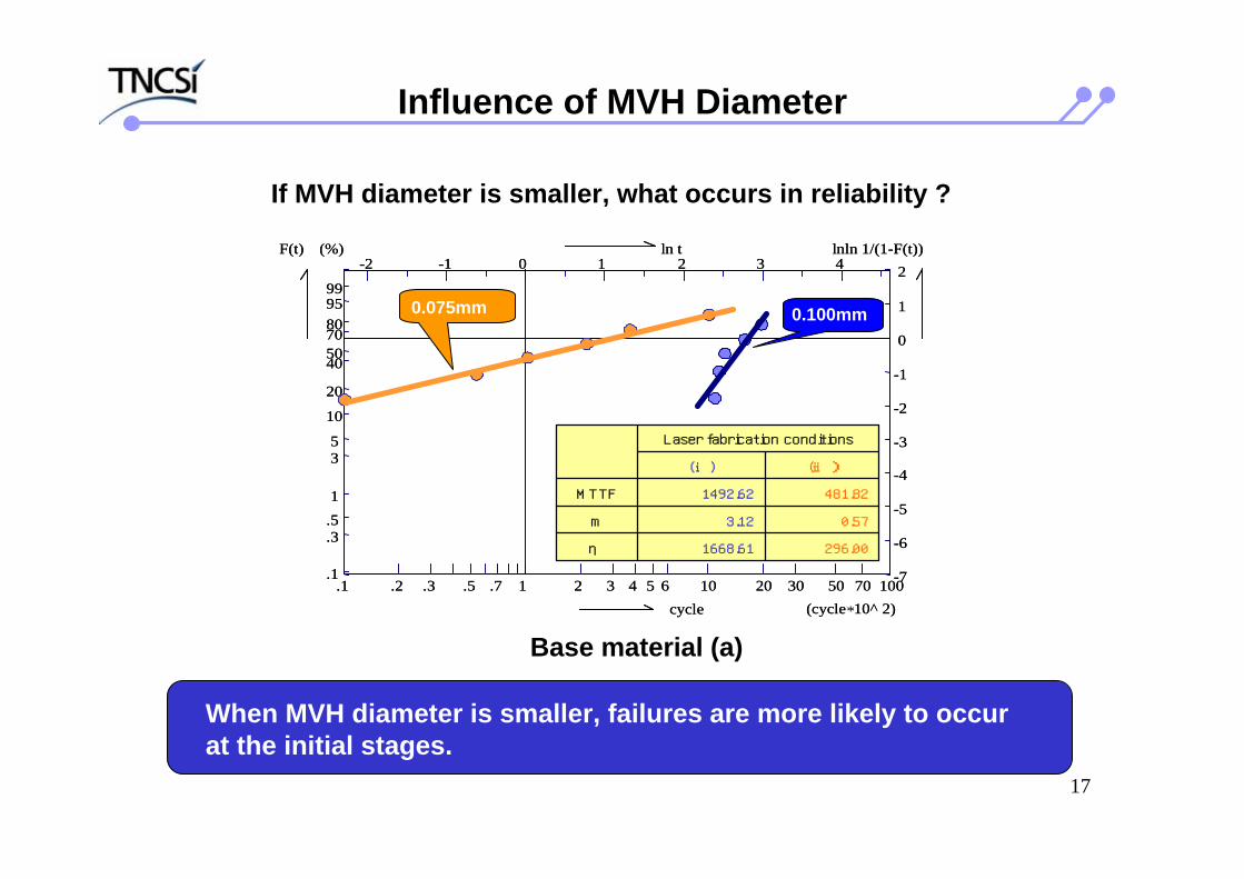
As a result of this evaluation, it was verified that the connection reliability was superior in the order of MVH, IVH and PTH. In order to enhance the total connection reliability, we believe that it is necessary to improve the connection reliability of PTH and IVH in particular. For both the PTH and the IVH process, it is generally said that a thinner board causes fewer problems. To verify this, we produced evaluation purpose PTH boards with a 1.6 mm board thickness. These thinner boards were achieved by making the prepreg thinner for the substrates (a) and (c) (see Table 4). It was ultimately verified that a thinner board provided superior reliability in connection. In order to find out the extent of failures as a function of smaller MVH, we made three-step stack via holes using base materials (a) and (c), each under the two types of laser fabrication conditions. The average value of MVH diameters obtained is given in Table 5. The evaluation revealed that the first failures happened during the 10th cycle on base material (a) and during the 58th cycle on base material (c). The results of the evaluation of the base material (a) are shown in Figure 9 as an example. Comparing the “m” values (i.e., shape parameters) on a Weibull distribution, we can see that under laser fabrication conditions (ii), when m < 1, failures occur early. In the case of laser fabrication conditions (i), m > 1, the occurrence of failures is relative to the elapse of time. Checking the failure mode under the laser fabrication condition (ii), it was found that the copper plated walls of the hole became thinner as a void occurred within the MVH (see Figure 10). The root cause was the difficulty in circulating the foaming solution and copper plating solution within MVH during the copper plating process due to the higher aspect ratio from a decreased MVH diameter. In promoting smaller diameters of MVH, attention must be paid to ensure the setting of the MVH diameter and the dielectric thickness. To achieve a stable volume production, it is also necessary to establish a quality assurance process aimed at eliminating voids within MVH. In order to satisfy the 200 cycle requirement of the DC current induced thermal cycling test, it is necessary to ensure the reliability of PTH or IVH and use either a high-Tg material or a material of low thermal expansion. With regard to MVH, an MVH diameter of approximately 0.100 mm is desirable to correspond with a thickness of 0.06 mm between build-up layers. It is necessary to carefully examine the manufacturing specifications of chip carrier applications since their design rules and base materials are different from those of general printed wiring boards.
Table 4 – MTTF
Table 5 – Average Values of MVH

S07-3-7
Figure 9 – Weibull Probability paper (Base Material (a); by Via Hole Diameters)
Figure 10 – Void of MVH
Insulation Reliability In line with the advancement of narrower pitches for surface mounting components, pitches between MVH and MVH are also becoming narrower. We have undertaken research to find out how the reduced distance between MVH and MVH affects insulation. We used the test pattern that combined MVH in a comb-type pattern as shown in the Figure 11 and in accordance with the design rules described in Table 6. Four kinds of base materials were used for the evaluation test, namely base materials (a), (b), (c) and (d), as shown in the Table 1. The thickness between build-up layers was 0.06 mm.
Table 6 – Design Rules

S07-3-8
Figure 11 – Test pattern
Evaluation method:
Moisture and Insulation Resistance (IR), Printed Board (IPC-TM-650, 2.6.3F) 2) Class 2, 50+/-5 degrees Celsius, 85 – 93% RH, DC 100V, for 7 days (168 hours). The test was conducted in accordance with all of the above conditions except for the test duration, which continued for up to 500 hours. We measured the IR of the samples every 10 minutes under the test environment.
Pre-treatment: 50 degrees Celsius for 24 hours
Criteria: No measling, blistering, delamination, etc. is allowed. Insulation resistance should be at least 500 x 106 ohms.
Sampling size: n = 6
The results of this evaluation are provided in Table 7. The evaluation found no failures on any of the samples for the 168 hours of testing that is the standard requirement for the IPC-TM-650 Environmental Test Method 2.6.3F. However, our longer test duration found that 1 out of every 6 samples of base material (a) with a 0.35 mm MVH pitch (a distance between hole walls of 0.25 mm), had a failure after 434 hours. When we checked the defective portion, a conductive anodic filament (CAF) was discovered (see the Figure 12). Because the results well satisfy the standard 168 hour requirement, we conclude that there is no problem with an MVH pitch of 0.35 mm or more (or a distance of at least 0.25 mm between hole walls) on any of the base materials. (See Figures 13-16) Insulation reliability apparently varies depending on the resin and the glass cloth within the base material. It will be important to select an appropriate base material in consideration of the customer’s requirements and the design rules.
Table 7 – Evaluation Results

S07-3-9
Figure 12 – Location where CAF Happened
Figure 13 – 0.35 mm MVH Pitch on Base material (a)
Figure 14 – 0.35 mm MVH Pitch on Base material (b)
Figure 15 – 0.35 mm MVH Pitch on Base material (c)

S07-3-10
Figure 16 – 0.35 mm MVH Pitch on Base material (d)
Conclusion The evaluation verified that the connection reliability was highest in MVH, followed by IVH, and then PTH. For the base material, a high-Tg material with low thermal expansion properties is recommended as no failure was found after completing a total of 2000 cycles. In general, the thicker the board, the more problems occur in IVH and PTH. To improve the reliability in products with a higher layer count, it is desirable to use base materials with both high-Tg and low thermal expansion properties. Assuming there is no restriction on the impedance specification or the like, we suggest, to improve connection reliability by reducing the total thickness, using a 0.06 mm thick inner layer material and a 0.06 mm thick prepreg. In promoting smaller diameters of MVH, the aspect ratio of MVH becomes higher, increasing the risk of a void on the copper plate, thus greater care is required in the setting of the thickness between the build-up layers. To allow for volume production, an MVH diameter of 0.100 mm is desirable if the thickness between the build-up layers is 0.06 mm. In order to realize a higher aspect ratio of MVH, consideration must be given to de-foaming during copper plating, the method for circulating the copper plating solution within MVH, and the reduction of glass projection from the hole walls. In regard to the insulation reliability, care is required in the selection of base materials even though no problem was found for an MVH pitch of up to 0.35 mm. To further enhance the reliability of high layer count build-up printed wiring boards, it is necessary to optimize the base materials in regard to the board thickness, PTH diameter, IVH diameter, MVH diameter, and copper plate thickness. By doing so, we hope to offer more attractive products and services in the future. References 1. IPC-TM-650 Environmental Test Methods 2.6.26 DC Current Induced Thermal Cycling--5/01 2. IPC-TM-650 Environmental Test Methods 2.6.3F Moisture and Insulation Resistance, Printed Boards--5/04

1
Tatsuo SUZUKI
Interconnection Reliability of HDI Printed Wiring Boards

2
Contents
Page
Ⅰ.Introduction 3-4
Ⅱ. Manufacturing Process 5
Ⅲ. Body
A. Interconnection Reliability 6-20
B. Insulation Reliability 21-26
Ⅳ.Conclusion 27-28

3
Background
Demand
Mounting parts・Higher pin counts
・Narrower pitches
PWB・Higher density
Build-up via-on-via structure
Application・Routers
・Telecommunication switches
(stacked via holes)
・Higher reliability
Interconnection reliability
Insulation reliability

4
Purpose of Study
実験計画法(直交表)に基づき、レーザービアのインピーダンスを検証(御社ご指示に基づく)
フィルドビア仕様(φ100μm)≒通常めっき2回仕様(φ125μm)を確認
It is necessary to establish some design rules , according to study materials and reliability.
Process control
Design rulesMaterials
High reliability

5
Manufacturing Process
Circuit patterning
Lamination
Window opening for laser drilling
Laser drilling
Filled plating
Circuit patterning
Repeat
Lamination
Drilling
Window opening for laser drilling
Laser drilling
Filled plating
Circuit patterningPTH MVH
(micro-via-hole)
IVH
Base material Copper Hole filling resin

6
Interconnection Reliability

7
Characteristic of Evaluation Board Materials
Tg measurement:TMA Method (Thermal Mechanical Analysis Method)
CTE: Coefficient of Thermal Expansion
Actual MeasurementMaterial Classification Tg
α1(<Tg) α2(>Tg)Base material a FR-4 131℃ 86ppm/℃ 264ppm/℃
b Halogen-free 152℃ 42ppm/℃ 200ppm/℃c High Tg FR-4 171℃ 78ppm/℃ 273ppm/℃d Low CTE 163℃ 30ppm/℃ 146ppm/℃
Hole filling resin Low CTE 151℃ 30ppm/℃ 100ppm/℃
CTE (Z-axis)

8
Total board thickness(layer1-layer16):2.0mm
IVH layer thickness(layer4-layer13):1.3mm
Layer Structure
Layer 1Layer 2Layer 3
Layer 16Layer 15Layer 14Layer 13
Layer 4
PTH IVHMVH(1st/2nd/3rd)
Base material Hole filling resin Copper
Build-upLayer1~4
Build-upLayer13~16

9
Design Rules
*We manufactured the build-up layers using 1 ply 0.06mm prepreg (#1080).
The maximum thickness was 0.08mm.
Item StandardPTH Finished diameter φ0.30mm
Pad diameter φ0.60mmPlating thickness 25μm
IVH Finished diameter φ0.20mmPad diameter φ0.60mmPlating thickness 25μm
MVH Finished diameter (top) φ0.110mmFinished diameter (bottom) φ0.090mmPad diameter φ0.30mmPlating thickness Filled via hole

10
Evaluation Method
IPC-TM-650, 2.6.26: The cycle time was 3 minutes of heating (max. 150 degreeCelsius) followed by 2 minutes cooling.
Pre-treatment: Ambient to 230 degree Celsius in 3 minutes x 3 cycles.The number of cycle: 2,000 cyclesCriteria: Resistance change is max. 10%Sample size: n = 6Evaluation pattern: Daisy chain pattern for PTH, IVH and MVH
DC current induced thermal cycling test
Room TEMP
150deg. Celsius
Heating-up3 minutes
Cooling-down2 minutes

11
Evaluation Result
・Failures occurred in order FR-4, high-Tg FR-4, halogen-free and low CTE.・When the number of build-up steps increases, failures are more likely to occur.
a b c d
PTH 191.84 962.65 694.58 pass
IVH 313.26 1175.54 1002.96 pass
MVH (1st step) pass pass pass pass
MVH (2nd step) pass pass pass pass
MVH (3rd step) 1492.62 pass pass pass
(cycle)
Base material
MTTF (mean time to failure)

12
Evaluation Result
Failures occurred in order PTH, IVH and three-step MVH.
- 2 - 1 0 1 2 3 4 ln t lnln 1/(1 - F(t))
- 7
- 6
- 5
- 4
- 3
- 2
- 1
0
1
2
.1 .2 .3 .5 .7 1 2 3 4 5 6 10 20 30 50 70 100t (t*10^ 2)
.1
.3
.51
35
10
20
405070809599
- 2 - 1 0 1 2 3 4 (%)F(t) (%)F(t) ln t lnln 1/(1 - F(t))
- 7
- 6
- 5
- 4
- 3
- 2
- 1
0
1
2
.1 .2 .3 .5 .7 1 2 3 4 5 6 10 20 30 50 70 100cycle (cycle*10^ 2)
.1
.3
.51
35
10
20
405070809599
1668.61336.42213.99η
3.126.423.26m
1492.62313.26191.84MTTF
MVHIVHPTH
*
- 2 - 1 0 1 2 3 4 ln t lnln 1/(1 - F(t))
- 7
- 6
- 5
- 4
- 3
- 2
- 1
0
1
2
.1 .2 .3 .5 .7 1 2 3 4 5 6 10 20 30 50 70 100t (t*10^ 2)
.1
.3
.51
35
10
20
405070809599
- 2 - 1 0 1 2 3 4 (%)F(t) (%)F(t) (%)F(t) (%)F(t) ln t lnln 1/(1 - F(t))lnln 1/(1 - F(t))
- 7
- 6
- 5
- 4
- 3
- 2
- 1
0
1
2
.1 .2 .3 .5 .7 1 2 3 4 5 6 10 20 30 50 70 100cycle (cycle*10^ 2)
.1
.3
.51
35
10
20
405070809599
1668.61336.42213.99η
3.126.423.26m
1492.62313.26191.84MTTF
MVHIVHPTH
*
Base material (a)

13
Failure Mode(PTH)
Corner crack
Barrel crack

14
Failure Mode(IVH)
Barrel crack
Corner crack

15
Failure Mode(MVH)
Corner crack
(lower via hole)
Corner crack
(upper via hole)

16
Solutions to Improve Reliability of PTH and IVH
Reliability can be improved by reducing PWB thickness.
The most important point is reliability improvement method of PTH and IVH .
The improvement method Total PWB thickness: 2.0mm ⇒ 1.6mm(using 0.06mm base material and prepreg)
MTTF(PTH)
Board thickness
a c
PTH 2.0mm 191.84 694.58
1.6mm 240.43 1051.46
(cycle)
Base material
Better
17
-2 -1 0 1 2 3 4 (%)F(t) ln t lnln 1/(1-F(t))
-7
-6
-5
-4
-3
-2
-1
0
1
2
.1 .2 .3 .5 .7 1 2 3 4 5 6 10 20 30 50 70 100cycle (cycle*10^ 2)
.1
.3
.51
35
10
20
405070809599
*
296.001668.61η
0.573.12m
481.821492.62MTTF
(ⅱ)(ⅰ)
Laser fabrication conditions
-2 -1 0 1 2 3 4 (%)F(t) ln t lnln 1/(1-F(t))
-7
-6
-5
-4
-3
-2
-1
0
1
2
.1 .2 .3 .5 .7 1 2 3 4 5 6 10 20 30 50 70 100cycle (cycle*10^ 2)
.1
.3
.51
35
10
20
405070809599
*
296.001668.61η
0.573.12m
481.821492.62MTTF
(ⅱ)(ⅰ)
Laser fabrication conditions
Influence of MVH Diameter
When MVH diameter is smaller, failures are more likely to occurat the initial stages.
If MVH diameter is smaller, what occurs in reliability ?
0.075mm 0.100mm
Base material (a)

18
The copper plated walls of the hole became thinner as a void occurred, when the MVH diameter was 0.075 mm.
.
Failure Mode(MVH)

19
Technical Theme
Manufacture technology・Prevention of the void
Normal(section) X-rays Void(section) X-rays
Void
The liquid circulation and de-foaming method in the MVH during the plating process.
Inspection technology・Inspection of the void
e.g. The void inspection is possible by using X-rays.

20
Section Summary
The result・Failures occurred in order FR-4, high-Tg FR-4, halogen-free and low CTE.・Failures occurred in order PTH, IVH and three-step MVH. ・When diameter of MVH is smaller, failures are more likely to occur at the initial stages.
The improvement methodAs for the PTH and IVH・High-Tg FR-4 or Low CTE ・Reducing board thickness.
As for the MVH・The aspect ratio at which the void does not occur needs to be set up. e.g. Aspect ratio 0.6 MVH diameter 0.100m ‐ Dielectric thickness 0.06mm.

21
Insulation Reliability

22
The number of MVH:
Vertical 20 rows
×
horizontal 20 rows
Total 400 places
Test pattern
Design rules
(Outer layer) (Inner layer)
Evaluation Board
MVHpitch
MVH hole Inner landdiameter
Outer landdiameter
Distance betweenMVH hole walls
0.50mm 0.10mm 0.30mm 0.30mm 0.40mm
0.45mm 0.10mm 0.25mm 0.25mm 0.35mm
0.40mm 0.10mm 0.20mm 0.20mm 0.30mm
0.35mm 0.10mm 0.15mm 0.15mm 0.25mm

23
・The test was conducted in accordance with the above conditions except for we carried out the test up to 500 hours.
・We measured insulation resistance of the samples every 10 minutes under the test environment.
IPC-TM-650, 2.6.3F Class2 50+/-5 degree Celsius 85 – 93% RH DC 100V 7 days (168 hours)
Pre-treatment: 50 degree Celsius for 24 hoursCriteria: No measling, blister, delamination, etc. are allowed.
Insulation resistance shall be 500 x 106 ohm or moreSampling size: n = 6
Moisture and Insulation Resistance Printed Board
Evaluation Method

24
CAF (conductive anodic filament) was found.
Evaluation Result and Failure Mode
a b c d
0.50mm pass pass pass pass
0.45mm pass pass pass pass
0.40mm pass pass pass pass
0.35mm NG 1/6(434hr)
pass pass pass
Base materialMVH pitch

25
1.0E+07
1.0E+08
1.0E+09
1.0E+10
1.0E+11
1.0E+12
1.0E+13
1.0E+14
0 100 200 300 400 500
Time[hr]
Res
istan
ce[Ω
]
sample 1sample 2sample 3sample 4sample 5sample 6
1.0E+07
1.0E+08
1.0E+09
1.0E+10
1.0E+11
1.0E+12
1.0E+13
1.0E+14
0 100 200 300 400 500
Time[hr]
Res
istan
ce[Ω
]
sample 1sample 2sample 3sample 4sample 5sample 6
1.0E+07
1.0E+08
1.0E+09
1.0E+10
1.0E+11
1.0E+12
1.0E+13
1.0E+14
0 100 200 300 400 500
Time[hr]
Res
istan
ce[Ω
]
sample 1sample 2sample 3sample 4sample 5sample 6
1.0E+07
1.0E+08
1.0E+09
1.0E+10
1.0E+11
1.0E+12
1.0E+13
1.0E+14
0 100 200 300 400 500
Time[hr]R
esist
ance
[Ω]
sample 1sample 2sample 3sample 4sample 5sample 6
434hr; 4.62E+07Ω
Insulation Resistance
0.35 mm MVH pitch on base material (a) 0.35 mm MVH pitch on base material (b)
0.35 mm MVH pitch on base material (c) 0.35 mm MVH pitch on base material (d)
The evaluation found no failures for the 168 hours of testing.
26
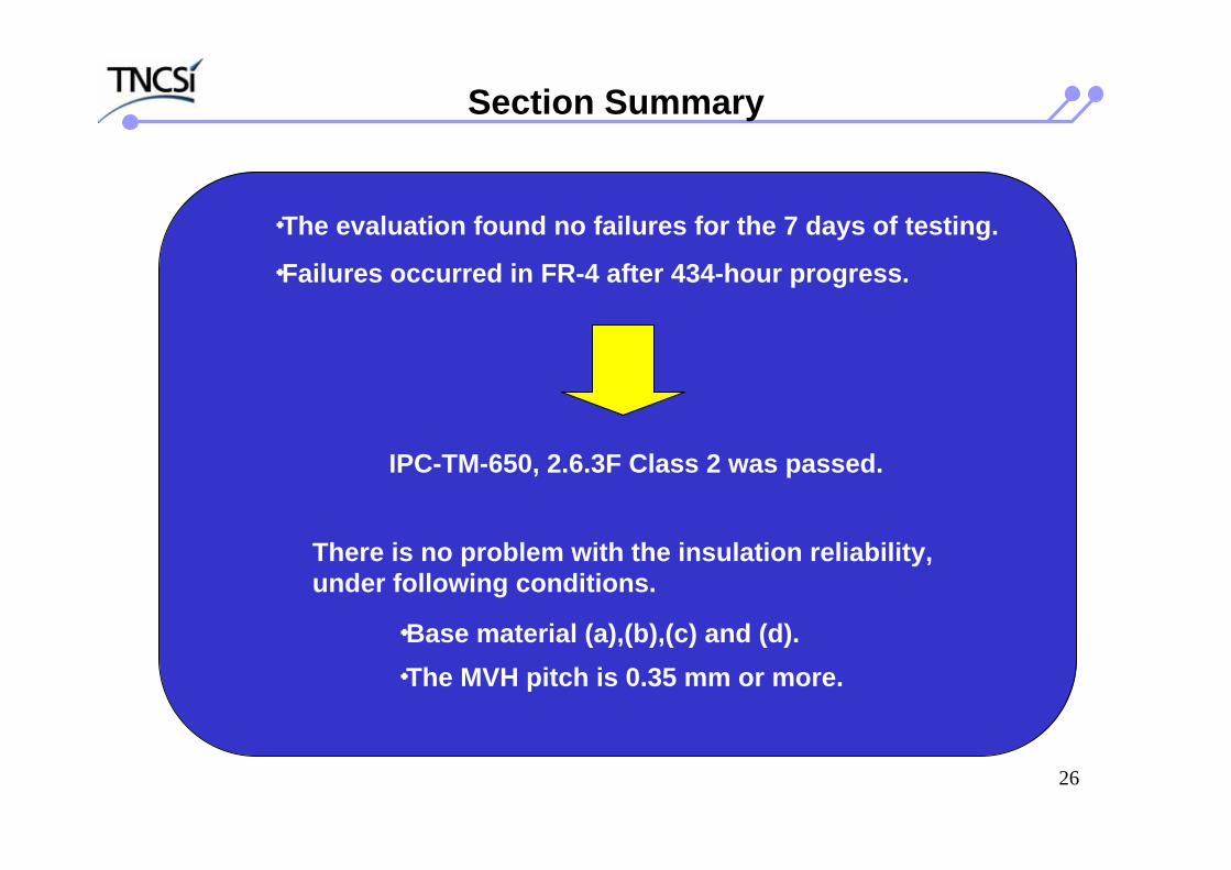
・The evaluation found no failures for the 7 days of testing.
・Failures occurred in FR-4 after 434-hour progress.
IPC-TM-650, 2.6.3F Class 2 was passed.
There is no problem with the insulation reliability, under following conditions.
・Base material (a),(b),(c) and (d).・The MVH pitch is 0.35 mm or more.
Section Summary

27
Conclusion
Recommendation for the higher reliability・Base material
High-Tg FR-4 with as low CTE as possible.
Thinner material as possible.
The MVH diameter is 0.100 mm is demanding if the thickness between the build-up layer is 0.06 mm.
・Design rules
Set up the aspect ratio which has a margin in MVH.

28
We hope to offer more highly reliable products and services in the future.
According to the demand of the customer for interconnectionreliability, we study what material should be used.
We will offer a highly reliable product at a competitive price.
Our Message


![Reliability Analysis of Multilayer Multistage Interconnection ...faculty.iauctb.ac.ir/faculty/Files/492/Board/Reliability...studied and adapted for networks-on-chip (NoCs) [5, 6].](https://static.fdocuments.in/doc/165x107/60c217627f96031ccd69e6a6/reliability-analysis-of-multilayer-multistage-interconnection-studied-and.jpg)