intelligent motion systems, inc. Excellence in … motion systems, inc. Excellence in Motion TM...
84
intelligent motion systems, inc. Excellence in Motion TM IM483 HIGH PERFORMANCE MICROSTEPPING DRIVE STANDARD DRIVER CONNECTOR OPTIONS DUAL STEP CLOCK INPUT VERSION COOLING SOLUTIONS ACCESSORIES OPERATING INSTRUCTIONS T 370 N. MAIN ST., PO BOX 457, MARLBOROUGH, CT 06447 PH. (860) 295-6102, FAX (860) 295-6107 Internet: http://www.imshome.com, E-Mail: [email protected] TM
Transcript of intelligent motion systems, inc. Excellence in … motion systems, inc. Excellence in Motion TM...

intelligent motion systems, inc.
Excellence in MotionTM
IM483HIGH PERFORMANCE MICROSTEPPING DRIVE
STANDARD DRIVERCONNECTOR OPTIONS
DUAL STEP CLOCK INPUT VERSIONCOOLING SOLUTIONS
ACCESSORIES
OPERATING INSTRUCTIONS
TM
370 N. MAIN ST., PO BOX 457, MARLBOROUGH, CT 06447PH. (860) 295-6102, FAX (860) 295-6107
Internet: http://www.imshome.com, E-Mail: [email protected]
TM

© Intelligent Motion Systems, Inc.All Rights Reserved
IM483 Operating InstructionsRevision R032306
The information in this book has been carefully checked and is believed to be accurate; however, no responsibility is assumed for inaccuracies.
Intelligent Motion Systems, Inc., reserves the right to make changes without further notice to any products herein to improve reliability, function or design. Intelligent Motion Systems, Inc., does not assume any liability arising out of the application or use of any product or circuit described herein; neither does it convey any license under its patent rights of others. Intelligent Motion Systems and are trademarks of Intelligent Motion Systems, Inc.
Intelligent Motion Systems, Inc.’s general policy does not recommend the use of its products in life support or aircraft applications wherein a failure or malfunction of the product may directly threaten life or injury. Per Intelligent Motion Systems, Inc.’s terms and conditions of sales, the user of Intelligent Motion Systems, Inc., products in life support or aircraft applications assumes all risks of such use and indemnifies Intelligent Motion Systems, Inc., against all damages.
Change Log
Date Revision Changes
03/23/2006 R032306 Updated IMS Contact info, warranty and disclaimer info on cover. Up-dated recommended IMS Motor Part Numbers.

1IM483 Operating Instructions Revision R032306
Table of Contents
Introduction............................................................................................... 5The IM483 ..................................................................................................................... 5Features and Benefits ................................................................................................... 5The Product Manual ...................................................................................................... 6The Product Manual ...................................................................................................... 6Notes and Warnings...................................................................................................... 7
Hardware Specifications........................................................................... 8Section Overview .......................................................................................................... 8Mechanical Specifications ............................................................................................. 8Electrical Specifications................................................................................................. 9Thermal Specifications ................................................................................................ 10Pin Assignment and Description ................................................................................. 10
Mounting The IM483 .............................................................................. 13Theory of Operation ............................................................................... 14
Section Overview ........................................................................................................ 14Circuit Operation ......................................................................................................... 14Microstep Select (MSEL) Inputs.................................................................................. 15Stepping ...................................................................................................................... 15Dual PWM Circuit ........................................................................................................ 16Fullstep Output Signal ................................................................................................. 17Timing.......................................................................................................................... 17
Power Supply Requirements.................................................................. 18Section Overview ........................................................................................................ 18Selecting a Power Supply ........................................................................................... 18Selecting an Opto Supply............................................................................................ 20Recommended Wiring................................................................................................. 21AC Line Filtering.......................................................................................................... 22
Motor Requirements............................................................................... 23Section Overview ........................................................................................................ 23Selecting a Motor ........................................................................................................ 23Motor Wiring ................................................................................................................ 28Connecting the Motor .................................................................................................. 28
Interfacing and Controlling the IM483 .................................................... 32Section Overview ........................................................................................................ 32Layout and Interface Guidelines.................................................................................. 32Motor Power Connection (+V) ..................................................................................... 33Configuring and Controlling the Output Current .......................................................... 34Controlling the Output Resolution ............................................................................... 39Interfacing and Using the Isolated Logic Inputs .......................................................... 41Connecting and Using the Fault Output ...................................................................... 47Full Step Output .......................................................................................................... 48Minimum Connections................................................................................................. 49
Troubleshooting...................................................................................... 50Section Overview ........................................................................................................ 50Basic Troubleshooting................................................................................................. 50Problem Symptoms and Possible Causes .................................................................. 50Contacting Technical Support ..................................................................................... 53The IMS Web Site ....................................................................................................... 53Returning Your Product to IMS ................................................................................... 53

2 IM483 Operating Instructions Revision R032306 3IM483 Operating Instructions Revision R032306
Appendix A: Standard Connection Options............................................ 54Appendix Overview ..................................................................................................... 54IM483-34P1................................................................................................................. 55IM483-8P2................................................................................................................... 60IM483-34P1-8P2 ......................................................................................................... 62IM483-PLG.................................................................................................................. 64
Appendix B: Input Options...................................................................... 66IM483-DC .................................................................................................................... 66
Appendix C: Cooling Solutions............................................................... 68H-4X Heat Sink Kit ...................................................................................................... 68Thermal Non-Isolating Pad (TN-48) ........................................................................... 68
Appendix D: Accessories ....................................................................... 69Appendix Overview ..................................................................................................... 69U3-CLP: Side-Mounting Clip ....................................................................................... 69BB-34-4P Breakout Board........................................................................................... 71PLG-R Removable Screw Terminal Set...................................................................... 73
Appendix E: Recommended Cable Configurations ................................ 74

2 IM483 Operating Instructions Revision R032306 3IM483 Operating Instructions Revision R032306
List Of Figures
Figure 2.1 IM483 Dimensions .................................................................................. 8Figure 2.2 IM483 Pin Configuration ....................................................................... 10Figure 3.1 Mounting Recommendations................................................................ 13Figure 4.1 IM483 Block Diagram ........................................................................... 14Figure 4.2 Recirculating PWM ............................................................................... 16Figure 4.3 Non-Recirculating PWM ....................................................................... 16Figure 6.1 Per Phase Winding Inductance ............................................................ 25Figure 6.2 8 Lead Motor Series Connections ........................................................ 29Figure 6.3 8 Lead Motor Parallel Connections....................................................... 29Figure 6.4 6 Lead Motor Half Coil (Higher Speed) Connections ........................... 30Figure 6.5 6 Lead Motor Full Coil (Higher Torque) Connections ........................... 30Figure 6.6 4 Lead Motor Connections.................................................................... 31Figure 7.1 IM483 Motor Power Connections ......................................................... 34Figure 7.2 Current Adjust Resistor Placement....................................................... 37Figure 7.3 Current Reduction Adjust Resistor Placement ..................................... 38Figure 7.4 MSEL Switch Showing 50 Microsteps/Step Selected........................... 39Figure 7.5 Optically Isolated Inputs........................................................................ 41Figure 7.6 Switch Interface .................................................................................... 44Figure 7.7 Open Collector Interface....................................................................... 45Figure 7.8 TTL Interface ........................................................................................ 45Figure 7.9 LYNX Interface ..................................................................................... 46Figure 7.10 The Fault Output Connected to an LED ............................................... 47Figure 7.11 The Full Step Output Connected to an Up/Down Counter ................... 48Figure 7.12 IM483 Minimum Required Connections................................................ 49Figure A.1 IM483-34P1 Connector P1 Mechanical Drawing.................................. 55Figure A.2 IM483-34P1 Connector P1 Pin Locations ............................................ 55FIgure A.3 MSEL Connection Using TTL Interface ................................................ 58Figure A.4 Cascading IM483-34P1 Drives Using the Step/Direction Outputs ....... 59Figure A.5 IM483-8P2 - Connector P1................................................................... 60Figure A.6 IM483-8P2 - Connector P2................................................................... 60Figure A.7 IM483-8P2 PCB Hole Pattern............................................................... 61Figure A.8 IM483-34P1-8P2 - Connector P1 ......................................................... 62Figure A.9 IM483-34P1-8P2 - Connector P2 ......................................................... 62Figure A.10 IM483-34P1-8P2 PCB Hole Pattern ..................................................... 63Figure A.11 IM483-PLG Connectors ........................................................................ 64Figure A.12 IM483-PLG Pin Location and Orientation............................................. 65Figure B.1 IM483-DC Connection .......................................................................... 67Figure C.1 H-4X Heat Sink ..................................................................................... 68Figure D.1 U3-CLP Mounting Hole Locations ........................................................ 69Figure D.2 Attaching the U3-CLP to the IM483...................................................... 70Figure D.3 Panal Mounting an IM483 Using the U3-CLP Clip Set ......................... 70Figure D.4 BB-34-4P Breakout Board Mechanical Specifications.......................... 71Figure D.5 BB-34-4P Pin Locations........................................................................ 72Figure D.6 BB-34-4P Mounting Diagram................................................................ 72

4 IM483 Operating Instructions Revision R032306 5IM483 Operating Instructions Revision R032306
List Of Tables
Table 2.1 Electrical Specifications .......................................................................... 9Table 2.2 IM483 Thermal Specifications .............................................................. 10Table 2.3 Connector P1 - Pin Assignment and Description.................................. 11Table 2.4 Connector P2 - Pin Assignment and Description.................................. 12Table 5.1 Motor Power Supply Requirements ...................................................... 19Table 5.2 +5 VDC Power Supply Requirements .................................................. 20Table 7.1 Current Adjust Resistor Values............................................................. 37Table 7.2 Microstep Resolution Switch Settings................................................... 40Table 7.3 Recommended Input Current Limiting Resistor Values........................ 42Table 7.4 Isolated Logic Input Timing................................................................... 43Table A.1 IM483-34P1 - Connector P1 Pin Assignment and Description............ 56Table B.1 IM483-DC - Connector P1 Pin Assignment and Description ................ 66

4 IM483 Operating Instructions Revision R032306 5IM483 Operating Instructions Revision R032306
F e a t u r e s a n d B en e f i t s
n Low Cost.
n Small Size 2.75” x 3.00” x 1.20” (69.9 x 76.2 x 30.5 mm).
n Advanced Surface Mount and ASIC Technology.
n High Input Voltage (+12 to +48VDC).
n High Output Current (3A RMS, 4A Peak).
n No Minimum Inductance.
Sec tion 1I n t r o d u c t i o n
Th e IM483
The IM483 is a high performance, yet low cost microstepping driver that utilizes surface mount ASIC technology. The IM483 is small, easy to interface and use, yet powerful enough to handle the most demanding applications.
The IM483 has 14 built-in mic-rostep resolutions (both binary and decimal). The resolution can be changed at any time without the need to reset the driver. This feature allows the user to rapidly move long distances, yet precisely position the motor at the end of travel without the expense of high performance controllers.
With the development of proprietary and patented circuits, ripple current has been minimized to reduce motor heating common with other de-signs, allowing the use of low inductance motors to improve high speed performance and system efficiency.
The IM483, because of its small size and low cost, can be used to increase accuracy and smoothness in systems using higher step angle motors. In many instances mechanical gearing can be replaced with mic-rostepping, reducing cost and eliminating potential maintenance.
Available as options for the IM483 are a variety of connector styles, a heat sink and thermal pad and a dual clock input version of the IM483. If in-telligent and/or closed loop control is needed the IM483 is available with on-board indexer (IM483I) and indexer/encoder (IM483IE) versions.
The IM483 was developed to provide designers with affordable, state-of-the-art technology for the competitive edge needed in today’s market.

6 IM483 Operating Instructions Revision R032306 7IM483 Operating Instructions Revision R032306
n FAULT Output.
n Optically Isolated Inputs.
n Single Supply.
n Up to 10MHz Step Clock Rate.
n Short Circuit and Over Temperature Protection.
n Microstep Resolution to 51,200 Steps/Rev.
n Microstep Resolutions can be Changed “On-The-Fly” With-out Loss of Motor Position.
n 20 kHz Chopping Rate.
n Automatically Switches Between Slow and Fast Decay for Unmatched Performance.
n 14 Selectable Resolutions Both in Decimal and Binary.
n Adjustable Automatic Current Reduction.
n At Full Step Output.
n Optional On-board Indexer and Encoder Feedback.
n CE Certified.
Th e P r o d u c t Manua l
The main sections of this manual address the standard IM483 driver, which come with 8 position screw terminals as a connection medium. The different connector, input options and accessories are covered in detail in the appendices.
The indexer (IM483I) and indexer/encoder (IM483IE) versions of the IM483 are not covered in this document, as they have their own manual.
Th e P r o d u c t Manua l
The IM483 product manual in its electronic format may be downloaded from the IMS website at http://www.imshome.com. This version includes a Bookmark feature that allows the reader to link from a Bookmarked Topic in the Table of Contents to a full description of that feature’s attributes and functions. You can also select a Topic directly from the Table of Contents Pages. Topics with a Bookmark function are further identifiable because the cursor changes from a normal pointer to a “finger” pointer when placed over the word.

6 IM483 Operating Instructions Revision R032306 7IM483 Operating Instructions Revision R032306
WARNING! The IM483 components are sensitive to ElectroStatic Discharge (ESD). All handling should be done at an ESD protected workstation.
WARNING! Hazardous voltage levels may be present if using an open frame power supply to power the IM483.
WARNING! Ensure that the power supply output voltage does not exceed the maximum input voltage of the IM483.
No t e s a n d Wa r n i n g s

8 IM483 Operating Instructions Revision R032306 9IM483 Operating Instructions Revision R032306
12
34
56
78
0.150(3.8)
2.45(62.23)
2.750(69.9)
1.00(25.4)
0.312(7.92)
0.290(7.4)
2.710(68.8)
3.00(76.2)
0.030(0.8)
4X Ø 0.160(4X Ø 4.1)
1.20(30.50)
0.410(10.4)
1734
1
0.025(0.6)
18
IM483-34P1
Sec tion 2Ha r dwa r e S p e c i f i c a t i o n s
Se c t i o n O v e r v i ew
This section will acquaint you with the dimensional information, pin de-scription, power, environmental and thermal requirements of the IM483. It is broken down as follows:
n Mechanical Specifications.n Electrical Specifications.n Thermal Specifications.n Pin Assignment and Description.
Mechan i c a l S p e c i f i c a t i o n s
Shown is the standard 8 position screw terminal set for the IM483. Dimensions and specifications for the different connection options are available in Appendix A: Standard Connection Options, of this document.
Dimensions are in inches, parenthesis dimensions are in millimeters.
Figure 2.1: IM483 Dimensions
8 IM483 Operating Instructions Revision R032306 9IM483 Operating Instructions Revision R032306
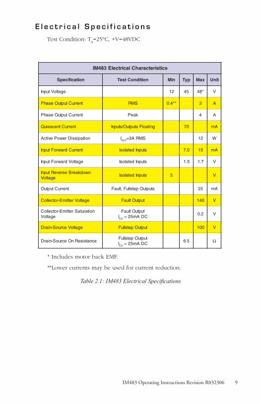
E l e c t r i c a l S p e c i f i c a t i o n s
Test Condition: TA=25°C, +V=48VDC
scitsiretcarahClacirtcelE384MI
noitacificepS noitidnoCtseT niM pyT xaM tinU
egatloVtupnI 21 54 *84 V
tnerruCtuptuOesahP SMR **4.0 3 A
tnerruCtuptuOesahP kaeP 4 A
tnerruCtnecseiuQ gnitaolFstuptuO/stupnI 07 Am
noitapissiDrewoPevitcA I TUO SMRA3= 21 W
tnerruCdrawroFtupnI stupnIdetalosI 0.7 51 Am
egatloVdrawroFtupnI stupnIdetalosI 5.1 7.1 V
nwodkaerBesreveRtupnIegatloV
stupnIdetalosI 5 V
tnerruCtuptuO stuptuOpetslluF,tluaF 52 Am
egatloVrettimE-rotcelloC tuptuOtluaF 041 V
noitarutaSrettimE-rotcelloCegatloV
tuptuOtluaFI SC CDAm52=
2.0 V
egatloVecruoS-niarD tuptuOpetslluF 001 V
ecnatsiseRnOecruoS-niarDtuptuOpetslluF
I SC CDAm52=5.6 Ω
Table 2.1: IM483 Electrical Specifications
* Includes motor back EMF.
**Lower currents may be used for current reduction.

10 IM483 Operating Instructions Revision R032306 11IM483 Operating Instructions Revision R032306
Th e r ma l S p e c i f i c a t i o n s
)C°(snoitacificepSlamrehT384MI
noitacificepS egnaR
erutarepmeTtneibmA °05+ot°0
erutarepmeTegarotS °521+ot°04-
erutarepmeTetalPmumixaM °07+
Table 2.2: IM483 Thermal Specifications
NOTE! Additional cooling may be required to limit the plate temperature to 70°C! An optional heat sink and thermal pad is available, see Appendix C: Cooling Solutions for details.
P i n A s s i g nmen t a n d De s c r i p t i o n
Figure 2.2: IM483 Pin Configuration
NOTE! This pin configuration diagram and table represent the pinout of any 8 position connector used for P1. If you purchased the IM483-34P1 option (34 Position Header) the pin configuration diagram and table is located in Appendix A: Standard Connection Options.
MSEL0MSEL1MSEL2MSEL3
ON
SW1
P1 P2
N/C - P1:1Step Clock - P1:2
Direction - P1:3Opto Supply - P1:4
Enable - P1:5Reset - P1:6
Fault Output - P1:7On-Full-Step Output - P1:8
P2:8 - Motor Ø AP2:7 - Motor ØP2:6 - Motor Ø BP2:5 - Motor ØP2:4 - +V (+12 to +48 VDC)P2:3 - GroundP2:2 - Current AdjustP2:1 - Current Reduction Adjust
A
B

10 IM483 Operating Instructions Revision R032306 11IM483 Operating Instructions Revision R032306
Conne c t o r P1
Table 2.3: Connector P1 - Pin Assignment and Descriptions
C384MI noitarugifnoC1Protcenno
#NIP NOITCNUF SLIATED
1 C/N .noitcennocoN
2 tupnIkcolCpetSrotomehtsecnavdatupnisihtnoegdegniogevitisopA
tnednepedsitnemercniehtfoezisehT.tnemercnieno.1WShctiwstcelesnoituloserehtfosgnittesehtnopu
3 tupnInoitceriD.rotomehtfonoitceridehtegnahcotdesusitupnisihTfonoitcennocehtnopusdnepedoslanoitceridlacisyhP
.sgnidniwrotomeht
4 ylppuSotpOdetalosiehtotrewopylppusotdesusitupniCDV5+sihTtsumeractub,desuebyamegatlovrehgihA.stupnicigol
.relpuoc-otpoehthguorhttnerrucehttimilotnekateb
5 elbasiD/elbanEtupnI
fonoitcestuptuoehtelbasid/elbaneotdesusitupnisihTeht,)nepo(etatsHGIHcigoLaninehW.revirdeht
tibihnitonseodtupnisiht,revewoH.delbaneerastuptuoehtybetadpulliwstuptuoeht,erofereht,kcolcpetseht
elihwrevirdehtotdeilppa)ynafi(seslupkcolcforebmun.delbasidsawti
6 tupnIteseRstuptuoesahp(revirdehtteserlliwtupnisiht,WOLnehW
laitinistitaeblliwrevirdeht,desaelernehW.)elbasidlliw.)NOBesahP,FFOAesahP(etats
7 tuptuOtluaFsahnoitidnoctiucrictrohsatahtsetacidnituptuosihT
.WOLevitcasituptuosihT.derrucco
8 tuptuOpetS-lluF-nO
sirevirdehtnehwsetacidnituptuorotcellocneposihTtnuocotdesuebnactuptuosihT.petslluftadenoitisop
sseldrager,devomsahrotomehtspetsllufforebmunehtsituptuosihT.neewtebnispetsorcimforebmunehtfo
.WOLevitca

12 IM483 Operating Instructions Revision R032306 13IM483 Operating Instructions Revision R032306
Conne c t o r P2
Table 2.4: Connector P2 - Pin Assignment and Descriptions
WARNING! The IM483 components are sensitive to ElectroStatic Discharge (ESD). All handling should be done at an ESD protected workstation.
WARNING! Hazardous voltage levels may be present if using an open frame power supply to power the IM483.
WARNING! Ensure that the power supply output voltage does not exceed the maximum input voltage of the IM483.
C384MI noitarugifnoC2Protcenno
#NIP NOITCNUF SLIATED
1 noitcudeRtnerruCtsujdA
rotsiserA.tupnItnemtsujdAnoitcudeRtnerruCesahPyletanoitroporplliw2nipdnanipsihtneewtebdetcennoc
yletamixorppasgnidniwrotomhtobnitnerrucehtecuderkcolcpetsehtfoegdeevitisoptsalehtretfasdnoces5.
nopudnepedlliwdecudertnerrucfotnuomaehT.tupni.desurotsiserehtfoeulaveht
2 tnerruCtnemtsujdA
detcennocsirotsiserA.tnemtsujdAtnerruCesahPmumixamehttsujdaot)DNG(3:2Pdnanipsihtneewteb
rotsiserA.rotomehtnitnerrucesahp TSUM eb384MIehtrotupnisihtotdetcennoc LLIW .tluafotnihctal
3 DNGylppusrewopehtfo,nruterro,dnuorgehT.dnuorGrewoP
.erehdetcennocsi
4 V+ .CDV84+ot21+.egatloVylppuSrotoM
5 BesahP .rotomgnippetsehtfoBØ
6 BesahP rotomgnippetsehtfoBØ
7 AesahP .rotomgnippetsehtfoAØ
8 AesahP .rotomgnippetsehtfoAØ

12 IM483 Operating Instructions Revision R032306 13IM483 Operating Instructions Revision R032306
Sec tion 3Moun t i n g T h e IM483
This section has recommended mounting instructions for the standard IM483. Special mounting instructions for any of the connection options for the IM483 are available in Appendix A: Standard Connection Options, of this document. An optional heat sink and thermal pad, the H-4X and TN-48, are available for the IM483. See Appendix C: Cooling Solutions, for details.
2 3 4 5 6 7 8Thermal PadTN-48 or Equivalent
Mounting Plateor Heatsink Surface
4 X #6 (M3) ThreadedHoles. (See Mechanical,
Figure 2.1 for Hole PatternDimensions)
A
B
C
A
B
C
#6 X 5/8 StainlessMachine Screw
#6 Split Lock Washer,Stainless (.04TH, .24 OD)
#6 Flat Washer,Stainless (.04 TH, .24 OD)
U.S. (4 ea.)
A
B
C
M3 X 0.5 StainlessMachine Screw
M3 Split Lock Washer,Stainless (.08TH, .6.20 OD)
M3 Flat Washer,Stainless (.0.8 TH, 6.20 OD)
Metric (4 ea.)
The torque specificationfor the mounting screwsis 5.0 to 7.0 lb-in (0.60 to0.80 N-m). Do not over-tighten screws!
Figure 3.1: Mounting Recommendations
NOTE! This diagram focuses on the standard IM483. The IM483-8P2 and IM483-34P1-8P2 feature connector pins which may be soldered directly into a user’s PCB design. Mounting details and a PCB hole pattern may be found in Appendix A: Standard Connection Options.

14 IM483 Operating Instructions Revision R032306 15IM483 Operating Instructions Revision R032306
Sec tion 4Th e o r y o f O p e r a t i o n
Se c t i o n O v e r v i ew
This section will cover the circuit operation for the IM483 microstepping driver.
n Circuit Operation.n Microstep Select Inputs.n Stepping.n Dual PWM Circuit.n Fullstep Output.n Timing.
C i r c u i t O p e r a t i o n
Microstepping drives have a much higher degree of suitability for ap-plications that require smooth operation and accurate positioning at low speeds than do half/fullstep drivers and reduction gearing. The IM483, which can to be set to microstep resolutions as high as 51,200 microsteps/rev (256 microsteps/step) using a 1.8° stepping motor, is ideal for such applications.
In order to subdivide motor steps into microsteps while maintaining positional accuracy, precise current control is required. The IM483 ac-complishes this by the use of a unique Dual PWM circuit built into the patented IM2000 Microstep Controller ASIC, which resides at the heart of the IM483. This PWM circuit uses alternating recirculating/non-recircu-lating modes to accurately regulate the current in the windings of a two phase stepping motor.
Figure 4.1: IM483 Block Diagram
INPUTLOGIC
INPUTLOGIC
ISOLATIONCIRCUITRY
SINE/COSINEPOSITION
GENERATOR
MICROSTEPRESOLUTIONSELECTION
STEP CLOCKDIRECTION
ENABLERESET
CURRENTCONTROL
USERINTERFACE
POWERSUPPLY
OPTOSUPPLY
20kHz CHOP.OSC
PROTECTIONCIRCUITIM2000 MICROSTEP
CONTROLLER
IM483 MICROSTEPPING DRIVER
PHASE A/BOUTPUT
CIRCUITRY
CURRENTSENSING
STEPPINGMOTOR
SHORTCIRCUIT
PROTECTION
OVER CURRENTPROTECTION
14 IM483 Operating Instructions Revision R032306 15IM483 Operating Instructions Revision R032306
Mi c r o s t e p S e l e c t (MSEL ) I n p u t s
Another unique feature of the IM2000 is the ability to change resolutions at any time. A resolution change can occur whether the motor is being clocked or is at rest. The change will not take place until the rising edge of the next step clock input. At this time, the new resolution is latched and implemented before the step clock pulse takes effect.
If a resolution is chosen such that the sine/cosine output of the IM2000 would not land on an electrical fullstep of the motor, then the IM2000 will automatically align itself to the full step position on the step clock pulse that would have caused the motor to rotate past the full step. The step clock pulses, from that point forward, will be equal to the selected resolution. This feature allows the user to switch resolutions at any time without having to keep track of sine/cosine location. Because of this, the On-Full-Step output of the IM483 can easily be used to monitor position.
Configuration settings for the Microstep Resolution are located in Section 7 of this document, Interfacing and Controlling the IM483.
S t e pp i n g
The IM2000 contains a built-in sine/cosine generator used for the genera-tion of Phase A and Phase B position reference. This digitally encoded 9 bit sine and 9 bit cosine signal is directly fed into a digital to analog converter.
The step clock (SCLK) and direction (DIR) inputs are buffered using Schmidt triggered buffers for increased noise immunity and are used to increment or decrement the sine/cosine position generator. The position generator is updated on the rising edge of the step clock input. It will increment or decrement by the amount specified by the microstep resolu-tion select (MSEL) inputs.
The direction (DIR) input determines the direction of the position genera-tor and hence the direction of the motor. The DIR input is synchronized to the SCLK input. On the rising edge of the SCLK input the state of the DIR input is latched in. The position generator will then look to see if there has been a change in direction and implement that change be-fore executing the next step. By utilizing this method to implement the direction change, the noise immunity is greatly increased and no physical change in the motor occurs if the direction line is toggled prior to the step clock input.
The enable/disable input does not affect the step clock input. The sine/cosine generator will continue to update if a signal is applied to the step clock input.
The IM2000 outputs both sine and cosine data simultaneously when applying a step clock input. Dual internal look-up tables are used to output a unique position for every step clock input to enhance system performance.

16 IM483 Operating Instructions Revision R032306 17IM483 Operating Instructions Revision R032306
Dua l PWM C i r c u i t
The IM2000 contains a unique dual PWM circuit that efficiently and accu-rately regulates the current in the windings of a two phase stepping motor. The internal PWM accomplishes this by using an alternating recirculating/non-recirculating mode to control the current.
Rec i r c u l a t i n g
In a recirculating PWM, the current in the windings is contained within the output bridge while the PWM is in its OFF state. (After the set current is reached.) This method of controlling the current is efficient when us-ing low inductance motors, but lacks response because of its inability to remove current from the windings on the downward cycle of the sine/cosine wave (See Figure 4.1).
Non - R e c i r c u l a t i n g
In a non-recirculating PWM, the current flows up through the bridge and back to the supply in the OFF phase of the cycle. This method of controlling current allows for much better response but re-duces efficiency and increas-
es current ripple, especially in lower inductance motors (See Figure 4.3).
The IM2000’s PWM utilizes the best features of both by combining recircu-lating and non-recirculating current control. On the rising edge of the sine/cosine waveform, the PWM will always be in a recirculating mode. This mode allows the driver to run at peak efficiency while maintaining minimum current ripple even with low inductance motors. On the downward cycle of the sine/cosine waveform, the PWM operates in a two part cycle. In the first part of its cycle, the PWM is in a non-recirculating mode to pull current from the motor windings. In the second part of the cycle the PWM Figure 4.3: Non-Recirculating PWM
DRIVE CURRENT
RECIRCULATION
Figure 4.2: Recirculating PWM
DRIVE CURRENT
RECIRCULATION

16 IM483 Operating Instructions Revision R032306 17IM483 Operating Instructions Revision R032306
reverts back to recirculating mode to increase efficiency and reduce cur-rent ripple.
The IM2000 will automatically change the non-recirculating pulse widths to compensate for changes in supply voltage and accommodate a wide variety of motor inductances. This method also allows for the use of very low inductance motors with your IM483 driver, while utilizing a 20kHz chopping rate which reduces motor heating but maintains high efficiency and low current ripple.
Fu l l s t ep Ou tpu t S i gna l
The fullstep output signal from the IM483 is an active high output at connector P1:8. This output will be TRUE for the duration of the full step. A full step occurs when either Phase A or Phase B crosses through zero (i.e. full current in one motor winding and zero current in the other winding). This fullstep position is a common position regardless of the microstep resolution selected.
The fullstep output can be used to count the number of mechanical fullsteps that the motor has traveled without the need to count the num-ber of microsteps in between. A controller that utilizes this output can greatly reduce its position tracking overhead, thus substantially increasing its throughput.
Interface guidelines and a sample application for the fullstep output are located in Section 7 of this document, Interfacing and Controlling the IM483.
T im ing
The direction and microstep resolution select inputs are synchronized with the positive going edge of the step clock input. When the step clock input goes HIGH, the direction and microstep resolution select inputs are latched. Further changes to these inputs are ignored until the next rising edge of the step clock input.
After these signals are latched, the IM483 looks to see if any changes have occurred to the direction and microstep resolution select inputs. If a change has occurred, the IM483 will execute the change before taking the next step. Only AFTER the change has been executed will the step be taken. If no change has occurred, the IM483 will simply take the next step. This feature works as an automatic debounce for the direction and microstep resolution select inputs.
The reset and enable inputs are asynchronous to any input and can be changed at any time.

18 IM483 Operating Instructions Revision R032306 19IM483 Operating Instructions Revision R032306
Sec tion 5Powe r S upp l y R e qu i r emen t s
Se c t i o n O v e r v i ew
This section covers the power supply requirements of the IM483. Precise wiring and connection details are to be found in Section 7: Interfacing and Controlling the IM483. The following is covered by this section:
n Selecting a Power Supply.
n Recommended Wiring.
n AC Line Filtering.
Se l e c t i n g a P owe r S upp l y
Se l e c t i n g a Mo t o r S u pp l y ( + V )
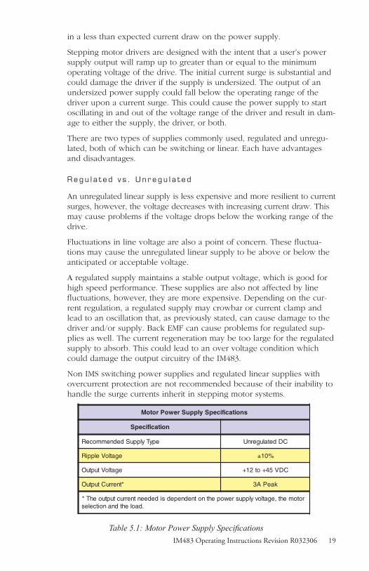
Proper selection of a power supply to be used in a motion system is as important as selecting the drive itself. When choosing a power supply for a stepping motor driver, there are several performance issues that must be addressed. An undersized power supply can lead to poor per-formance and possibly even damage to your drive.
Th e P owe r S u p p l y - Mo t o r R e l a t i o n s h i p
Motor windings can basically be viewed as inductors. Winding resistance and inductance result in an L/R time constant that resists the change in current. To effectively manipulate the rate of charge, the voltage applied is increased. When traveling at high speeds, there is less time between steps to reach current. The point where the rate of commutation does not allow the driver to reach full current is referred to as voltage mode. Ide-ally you want to be in current mode, which is when the drive is achiev-ing the desired current between steps. Simply stated, a higher voltage will decrease the time it takes to charge the coil and, therefore, will allow for higher torque at higher speeds.
Another characteristic of all motors is back EMF. Back EMF is a source of current that can push the output of a power supply beyond the maxi-mum operating voltage of the driver. As a result, damage to the stepper driver could occur over a period of time.
Th e P owe r S u p p l y - D r i v e r R e l a t i o n s h i p
The IM483 is very current efficient as far as the power supply is con-cerned. Once the motor has charged one or both windings of the motor, all the power supply has to do is replace losses in the system. The charged winding acts as an energy storage in that the current will recircu-late within the bridge and in and out of each phase reservoir. This results
18 IM483 Operating Instructions Revision R032306 19IM483 Operating Instructions Revision R032306
in a less than expected current draw on the power supply.
Stepping motor drivers are designed with the intent that a user’s power supply output will ramp up to greater than or equal to the minimum operating voltage of the drive. The initial current surge is substantial and could damage the driver if the supply is undersized. The output of an undersized power supply could fall below the operating range of the driver upon a current surge. This could cause the power supply to start oscillating in and out of the voltage range of the driver and result in dam-age to either the supply, the driver, or both.
There are two types of supplies commonly used, regulated and unregu-lated, both of which can be switching or linear. Each have advantages and disadvantages.
Regu l a t e d v s . U n r e g u l a t e d
An unregulated linear supply is less expensive and more resilient to current surges, however, the voltage decreases with increasing current draw. This may cause problems if the voltage drops below the working range of the drive.
Fluctuations in line voltage are also a point of concern. These fluctua-tions may cause the unregulated linear supply to be above or below the anticipated or acceptable voltage.
A regulated supply maintains a stable output voltage, which is good for high speed performance. These supplies are also not affected by line fluctuations, however, they are more expensive. Depending on the cur-rent regulation, a regulated supply may crowbar or current clamp and lead to an oscillation that, as previously stated, can cause damage to the driver and/or supply. Back EMF can cause problems for regulated sup-plies as well. The current regeneration may be too large for the regulated supply to absorb. This could lead to an over voltage condition which could damage the output circuitry of the IM483.
Non IMS switching power supplies and regulated linear supplies with overcurrent protection are not recommended because of their inability to handle the surge currents inherit in stepping motor systems.
Table 5.1: Motor Power Supply Specifications
snoitacificepSylppuSrewoProtoM
noitacificepS
epyTylppuSdednemmoceR CDdetalugernU
egatloVelppiR %01±
egatloVtuptuO CDV54+ot21+
*tnerruCtuptuO kaePA3
rotomeht,egatlovylppusrewopehtnotnednepedsidedeentnerructuptuoehT*.daolehtdnanoitceles
20 IM483 Operating Instructions Revision R032306 21IM483 Operating Instructions Revision R032306
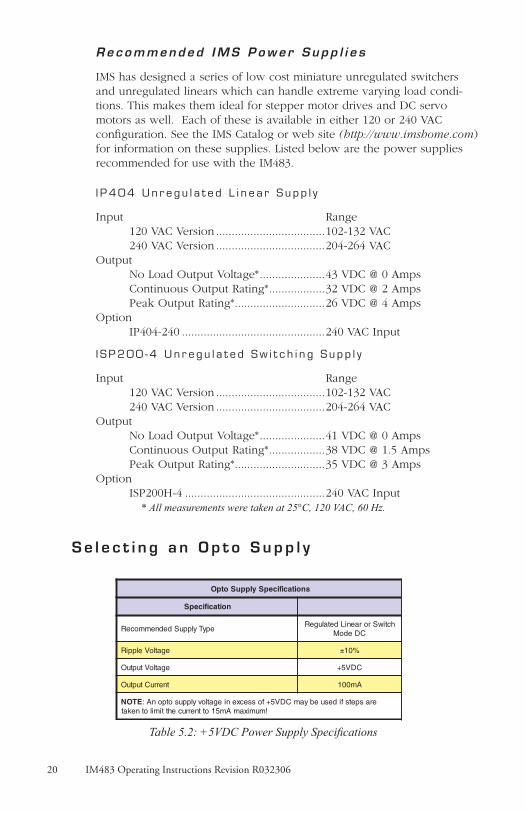
Recommended IMS Powe r S upp l i e s
IMS has designed a series of low cost miniature unregulated switchers and unregulated linears which can handle extreme varying load condi-tions. This makes them ideal for stepper motor drives and DC servo motors as well. Each of these is available in either 120 or 240 VAC configuration. See the IMS Catalog or web site (http://www.imshome.com) for information on these supplies. Listed below are the power supplies recommended for use with the IM483.
I P 404 Un r e g u l a t e d L i n e a r S u p p l y
Input Range 120 VAC Version ...................................102-132 VAC 240 VAC Version ...................................204-264 VACOutput No Load Output Voltage*.....................43 VDC @ 0 Amps Continuous Output Rating*..................32 VDC @ 2 Amps Peak Output Rating*.............................26 VDC @ 4 AmpsOption IP404-240 ..............................................240 VAC Input
I S P200 -4 Un r e g u l a t e d Sw i t c h i n g S u p p l y
Input Range 120 VAC Version ...................................102-132 VAC 240 VAC Version ...................................204-264 VACOutput No Load Output Voltage*.....................41 VDC @ 0 Amps Continuous Output Rating*..................38 VDC @ 1.5 Amps Peak Output Rating*.............................35 VDC @ 3 AmpsOption ISP200H-4 .............................................240 VAC Input
* All measurements were taken at 25°C, 120 VAC, 60 Hz.
Se l e c t i n g a n Op t o S u pp l y
Table 5.2: +5VDC Power Supply Specifications
snoitacificepSylppuSotpO
noitacificepS
epyTylppuSdednemmoceRhctiwSroraeniLdetalugeR
CDedoM
egatloVelppiR %01±
egatloVtuptuO CDV5+
tnerruCtuptuO Am001
ETON eraspetsfidesuebyamCDV5+fossecxeniegatlovylppusotponA:!mumixamAm51ottnerrucehttimilotnekat

20 IM483 Operating Instructions Revision R032306 21IM483 Operating Instructions Revision R032306
Recommended W i r i n g
Ru l e s o f W i r i n g a n d S h i e l d i n g
Noise is always present in a system that involves both high power and small signal circuitry. Regardless of the power configuration used for your system, there are some wiring and shielding rules that should be fol-lowed to keep the noise-to-signal ratio as small as possible.
Ru l e s o f W i r i n g
n Power supply and motor wiring should be shielded twisted pairs run separately from signal carrying wires.
n A minimum of 1 twist per inch is recommended.
n Motor wiring should be shielded twisted pairs using 20-gauge wire or, for distance greater than 5 feet, 18 gauge or better.
n Power ground return should be as short as possible to estab-lished ground.
n Power supply wiring should be shielded twisted pairs. Use 18 gauge wire if load is less than 4 amps, or 16 gauge for more than 4 amps.
n Do not “Daisy-Chain” power wiring to system components.
Ru l e s o f S h i e l d i n g
n The shield must be tied to zero-signal reference potential. In order for shielding to be effective, it is necessary for the signal to be earthed or grounded.
n Do not assume that earth ground is true earth ground. De-pending on the distance to the main power cabinet, it may be necessary to sink a ground rod at a critical location.
n The shield must be connected so that shield currents drain to signal-earth connections.
n The number of separate shields required in a system is equal to the number of independent signals being processed plus one for each power entrance.
n The shield should be tied to a single point to prevent ground loops.
n A second shield can be used over the primary shield, how-ever, the second shield is tied to ground at both ends.
Recommended P owe r S u p p l y C a b l e s
Power supply cables must not run parallel to logic level wiring as noise will be coupled onto the logic signals from the power supply cables.
22 IM483 Operating Instructions Revision R032306 23IM483 Operating Instructions Revision R032306
WARNING! Verify that the power supply wiring is correct prior to power application. If +V and GND are connected in reverse order, catastrophic damage to the IM483 may occur! Ensure that the power supply output voltage does not exceed +48 VDC, which is the maximum input voltage of the IM483!
WARNING! Hazardous voltage levels may be present if using an open frame power supply to power the IM483!
If more than one driver is to be connected to the same power supply, run separate power and ground leads to each driver from the power sup-ply. The following twisted pair jacketed Belden cable (or equivalent) are recommended for use with the IM483.
n Belden Part# 9740 or equivalent 18 Gauge
AC L i n e F i l t e r i n g
Since the output voltage of an unregulated power supply will vary with the AC input applied, it is recommended that an AC line filter be used to prevent damage to the IM483 due to a lightning strike or power surge.

22 IM483 Operating Instructions Revision R032306 23IM483 Operating Instructions Revision R032306
Sec tion 6Moto r R e qu i r emen t s
Se c t i o n O v e r v i ew
This section covers the motor configurations for the IM483.
n Selecting a Motor.
n Motor Wiring.
n Connecting the Motor.
Se l e c t i n g a Mo t o r
When selecting a stepper motor for your application, there are several factors that need to be taken into consideration:
n How will the motor be coupled to the load?
n How much torque is required to move the load?
n How fast does the load need to move or accelerate?
n What degree of accuracy is required when positioning the load?
While determining the answers to these and other questions is beyond the scope of this document, they are details that you must know in order to select a motor that is appropriate for your application. These details will affect everything from the power supply voltage to the type and wir-ing configuration of your stepper motor. The current and microstepping settings of your IM483 drive will also be affected.
Ty p e s a n d C on s t r u c t i o n o f S t e p p i n g Mo t o r s
The stepping motor, while classed as a DC motor, is actually an AC mo-tor that is operated by trains of pulses. Although it is called a “stepping motor”, it is in reality a polyphase synchronous motor. This means it has multiple phases wound in the stator and the rotor is dragged along in synchronism with the rotating magnetic field. The IM483 is designed to work with the following types of stepping motors:
1) Permanent Magnet (PM)
2) Hybrid Stepping Motors

24 IM483 Operating Instructions Revision R032306 25IM483 Operating Instructions Revision R032306
Hybrid stepping motors combine the features of the PM stepping motors with the features of another type of stepping motor called a variable re-luctance motor (VR). VR motors are low torque and load capacity motors which are typically used in instrumentation. The IM483 cannot be used with VR motors as they have no permanent magnet.
On hybrid motors, the phases are wound on toothed segments of the stator assembly. The rotor consists of a permanent magnet with a toothed outer surface which allows precision motion accurate to within ± 3 percent. Hybrid stepping motors are available with step angles vary-ing from 0.45° to 15° with 1.8° being the most commonly used. Torque capacity in hybrid steppers ranges from 5 - 8000 ounce-inches. Because of their smaller step angles, hybrid motors have a higher degree of suit-ability in applications where precise load positioning and smooth motion is required.
S i z i n g a Mo t o r f o r Yo u r S y s t em
The IM483 is a bipolar driver which works equally well with both bipolar and unipolar motors (i.e. 8 and 4 lead motors, and 6 lead center tapped motors).
To maintain a given set motor current, the IM483 chops the voltage using a constant 20kHz chopping frequency and a varying duty cycle. Duty cycles that exceed 50% can cause unstable chopping. This character-istic is directly related to the motor’s winding inductance. In order to avoid this situation, it is necessary to choose a motor with a low winding inductance. The lower the winding inductance, the higher the step rate possible.
W ind i n g I n d u c t a n c e
Since the IM483 is a constant current source, it is not necessary to use a motor that is rated at the same voltage as the supply voltage. What is important is that the IM483 is set to the motor’s rated current. See Section 7: Interfacing and Controlling the IM483 for more details.
As was discussed in the previous section, Power Supply Requirements, the higher the voltage used the faster the current can flow through the motor windings. This in turn means a higher step rate, or motor speed. Care should be taken not to exceed the maximum voltage of the driver. There-fore, in choosing a motor for a system design, the best performance for a specified torque is a motor with the lowest possible winding inductance used in conjunction with highest possible driver voltage.
The winding inductance will determine the motor type and wiring configu-ration best suited for your system. While the equation used to size a motor for your system is quite simple, several factors fall into play at this point.
The winding inductance of a motor is rated in milliHenrys (mH) per Phase. The amount of inductance will depend on the wiring configuration of the motor.

24 IM483 Operating Instructions Revision R032306 25IM483 Operating Instructions Revision R032306
Figure 6.1 A & B: Per Phase Winding Inductance
The per phase winding inductance specified may be different than the per phase inductance seen by your IM483 driver depending on the wiring configuration used. Your calculations must allow for the actual inductance that the driver will see based upon the wiring configuration.
Figure 6.1A shows a stepper motor in a series configuration. In this configuration, the per phase inductance will be 4 times that specified. For example: a stepping motor has a specified per phase inductance of 1.47mH. In this configuration the driver will see 5.88 mH per phase.
Figure 6.1B shows an 8 lead motor wired in parallel. Using this configu-ration the per phase inductance seen by the driver will be as specified.
Using the following equation we will show an example of sizing a motor for a IM483 used with an unregulated power supply with a minimum voltage (+V) of 18 VDC:
.2 X 18 = 3.6 mH
The recommended per phase winding inductance we can use is 3.6 mH.
Maximum Motor Inductance (mH per Phase) =.2 X Minimum Supply Voltage
NOTE: In calculating the maximum phase inductance, the minimum supply output voltage should be used when using an unregulated supply.
PHASE A
PHASE A
PHASE B
PHASE B
8 Lead Stepping MotorSeries Configuration
8 Lead Stepping MotorParallel Configuration
PHASE A
PHASE A
PHASE B
PHASE B
(Note: This example alsoapplies to the 6 lead motorfull copper configuration andto 4 lead stepping motors)
(Note: This example alsoapplies to the 6 lead motorhalf copper configuration)
Specified Per PhaseInductance
Specified Per PhaseInductance
Actual InductanceSeen By the Driver
Actual InductanceSeen By the Driver
A B
26 IM483 Operating Instructions Revision R032306 27IM483 Operating Instructions Revision R032306
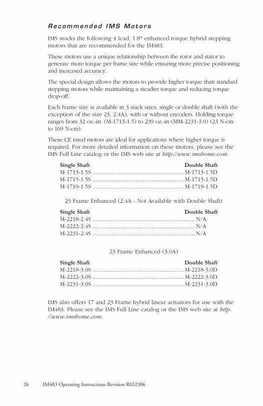
Recommended IMS Mo t o r s
IMS stocks the following 4 lead, 1.8° enhanced torque hybrid stepping motors that are recommended for the IM483.
These motors use a unique relationship between the rotor and stator to generate more torque per frame size while ensuring more precise positioning and increased accuracy.
The special design allows the motors to provide higher torque than standard stepping motors while maintaining a steadier torque and reducing torque drop-off.
Each frame size is available in 3 stack sizes, single or double shaft (with the exception of the size 23, 2.4A), with or without encoders. Holding torque ranges from 32 oz.-in. (M-1713-1.5) to 239 oz.-in (MM-2231-3.0) (23 N-cm to 169 N-cm).
These CE rated motors are ideal for applications where higher torque is required. For more detailed information on these motors, please see the IMS Full Line catalog or the IMS web site at http://www.imshome.com.
Single Shaft Double ShaftM-1713-1.5S ...........................................................M-1713-1.5DM-1715-1.5S ...........................................................M-1715-1.5DM-1719-1.5S ...........................................................M-1719-1.5D
23 Frame Enhanced (2.4A - Not Available with Double Shaft)
Single Shaft Double ShaftM-2218-2.4S ..................................................................N/AM-2222-2.4S ..................................................................N/AM-2231-2.4S ..................................................................N/A
23 Frame Enhanced (3.0A)
Single Shaft Double ShaftM-2218-3.0S ...........................................................M-2218-3.0DM-2222-3.0S ...........................................................M-2222-3.0DM-2231-3.0S ...........................................................M-2231-3.0D
IMS also offers 17 and 23 Frame hybrid linear actuators for use with the IM483. Please see the IMS Full Line catalog or the IMS web site at http://www.imshome.com.

26 IM483 Operating Instructions Revision R032306 27IM483 Operating Instructions Revision R032306
IMS I n s i d e O u t S t e p p e r Mo t o r s
The new inside out stepper (IOS) motor was designed by IMS to bring versatility to stepper motors using a unique multi-functional, hollow core design.
This versatile new motor can be converted to a ball screw linear actua-tor by mounting a miniature ball screw to the front shaft face. Ball screw linear actuators offer long life, high efficiency, and can be field retrofit-ted. There is no need to throw the motor away due to wear of the nut or screw.
The IOS motors offer the following features:
n The shaft face diameter offers a wide choice of threaded hole patterns for coupling.
n The IOS motor can be direct coupled in applications within the torque range of the motor, eliminating couplings and increasing system efficiency.
n The IOS motor can replace gearboxes in applications where gearboxes are used for inertia damping between the motor and the load. The induced backlash from the gearbox is eliminated providing improved bi-directional position accu-racy.
n Electrical or pnuematic lines can be directed through the center of the motor enabling the motors to be stacked end-to-end or applied in robotic end effector applications. The through hole is stationary, preventing cables from being chaffed by a moving hollow shaft.
n Light beams can be directed through the motor for refraction by a mirror or filter wheel mounted on the shaft mounting face.
n The IOS motor is adaptable to valves enabling the valve stem to protrude above the motor frame. The stem can be retrofitted with a dial indicator showing valve position.
n The motor is compatible with IMS bipolar drivers, keeping the system cost low.
n The IOS motor can operate up to 3000 rpm’s.
The IOS motor is available in the following frames:
Frame Size IMS PN17 Frame ................................................................M3-1713-IOS23 Frame ................................................................M3-2220-IOS
28 IM483 Operating Instructions Revision R032306 29IM483 Operating Instructions Revision R032306
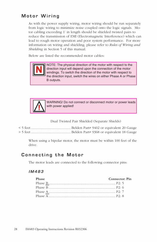
WARNING! Do not connect or disconnect motor or power leads with power applied!
NOTE: The physical direction of the motor with respect to the direction input will depend upon the connection of the motor windings. To switch the direction of the motor with respect to the direction input, switch the wires on either Phase A or Phase B outputs.
Moto r W i r i n g
As with the power supply wiring, motor wiring should be run separately from logic wiring to minimize noise coupled onto the logic signals. Mo-tor cabling exceeding 1’ in length should be shielded twisted pairs to reduce the transmission of EMI (Electromagnetic Interference) which can lead to rough motor operation and poor system performance. For more information on wiring and shielding, please refer to Rules of Wiring and Shielding in Section 5 of this manual.
Below are listed the recommended motor cables:
Dual Twisted Pair Shielded (Separate Shields)
< 5 feet ........................................... Belden Part# 9402 or equivalent 20 Gauge> 5 feet ........................................... Belden Part# 9368 or equivalent 18 Gauge
When using a bipolar motor, the motor must be within 100 feet of the drive.
Conne c t i n g t h e Mo t o r
The motor leads are connected to the following connector pins:
IM483
Phase Connector: PinPhase B ........................................................................ P2: 5Phase B ........................................................................ P2: 6Phase A ........................................................................ P2: 7Phase A ........................................................................ P2: 8

28 IM483 Operating Instructions Revision R032306 29IM483 Operating Instructions Revision R032306
8 L e a d Mo t o r s
8 lead motors offer a high degree of flexibility to the system designer in that they may be connected in series or parallel, thus satisfying a wide range of applications.
Se r i e s C o nn e c t i o n
A series motor configuration would typically be used in applications where a higher torque at lower speeds is required. Because this configu-ration has the most inductance, the performance will start to degrade at higher speeds. Use the per phase (or unipolar) current rating as the peak
output current, or multiply the bipolar current rating by 1.4 to determine the peak output current.
Pa r a l l e l C o n n e c t i o n
An 8 lead motor in a parallel configuration offers a more stable, but lower torque at lower speeds. But because of the lower inductance, there will be higher torque at higher speeds. Multiply the per phase (or unipolar) current rating by 1.96, or the bipolar current rating by 1.4, to determine the peak output current.
Figure 6.3: 8 Lead Motor Parallel Connections
Figure 6.2: 8 Lead Motor Series Connections
PHASE A
PHASE A
PHASE B
PHASE B
PHASE A
PHASE A
PHASE B
PHASE B

30 IM483 Operating Instructions Revision R032306 31IM483 Operating Instructions Revision R032306
6 L e a d Mo t o r s
Like 8 lead stepping motors, 6 lead motors have two configurations avail-able for high speed or high torque operation. The higher speed configu-ration, or half coil, is so described because it uses one half of the motor’s inductor windings. The higher torque configuration, or full coil, uses the full windings of the phases.
Ha l f C o i l C o n f i g u r a t i o n
As previously stated, the half coil configuration uses 50% of the mo-tor phase windings. This gives lower inductance, hence, lower torque output. Like the parallel connection of 8 lead motor, the torque output will be more stable at higher speeds. This configuration is also referred to as half copper. In setting the driver output current multiply the speci-fied per phase (or unipolar) current rating by 1.4 to determine the peak output current.
F u l l C o i l C o n f i g u r a t i o n
The full coil configuration on a six lead motor should be used in applica-tions where higher torque at lower speeds is desired. This configuration is also referred to as full copper. Use the per phase (or unipolar) current rating as the peak output current.
Figure 6.5: 6 Lead Full Coil (Higher Torque) Motor Connections
Figure 6.4: 6 Lead Half Coil (Higher Speed) Motor Connections
PHASE A
NO CONNECTION
NO CONNECTION
PHASE A
PHASE BPHASE B
PHASE ANO CONNECTION
NO CONNECTION
PHASE A
PHASE B
PHASE B
30 IM483 Operating Instructions Revision R032306 31IM483 Operating Instructions Revision R032306
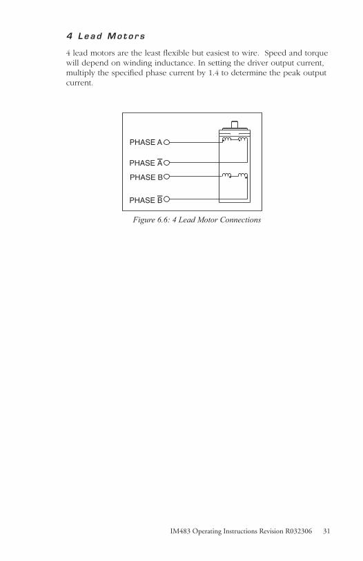
4 L e a d Mo t o r s
4 lead motors are the least flexible but easiest to wire. Speed and torque will depend on winding inductance. In setting the driver output current, multiply the specified phase current by 1.4 to determine the peak output current.
Figure 6.6: 4 Lead Motor Connections
PHASE A
PHASE A
PHASE B
PHASE B

32 IM483 Operating Instructions Revision R032306 33IM483 Operating Instructions Revision R032306
Sec tion 7I n t e r f a c i n g and Con t r o l l i n g t h e
IM483
Se c t i o n O v e r v i ew
This section covers the interface connections, configuration and control signals of the IM483. Covered are:
n Layout and Interface Guidelines.
n Motor Power Connection (+V).
n Controlling the Output Current
n Controlling the Output Resolution.
n Logic Interface Connection and Use.
n Using the Fault Output.
n Using the On-Fullstep Output.
n Minimum Required Connections.
L a y o u t a n d I n t e r f a c e Gu i d e l i n e s
Logic level signals should not run parallel to motor phase signals. The motor phase signals will couple noise onto the logic level signals. This will cause rough motor motion and unreliable system operation. The mo-tor phase signals should be run as pairs.
When leaving the driver module, motor cables should not run paral-lel with other wires. Phases should be wired using twisted pairs. If motor cabling in excess of one foot is required, motor cabling should be shielded twisted pairs to reduce the transmission of EMI. The shield must be tied to AC ground at the driver end only, or the supply ground if AC ground is not available. The motor end must be left floating.
If more than one driver is connected to the power supply, separate power and ground connections from each driver to the power supply should be used. Do not “daisy chain”.
The power supply cables need to be a twisted pair if power is connected from a source external to the board. If multiple drivers are used with an external power source and it is not possible to run separate power and ground connections to each driver, a low impedance electrolytic capaci-tor equivalent to two times the total capacitance of all driver capacitors and of equal voltage must be placed at the power input of the board.

32 IM483 Operating Instructions Revision R032306 33IM483 Operating Instructions Revision R032306
Recommended W i r i n g P r a c t i c e s
The following wiring/cabling is recommended for use with the IM483:
Mo t o r P owe r
Belden Part# 9740 or equivalent 18 AWG (shielded twisted pair).
Mo t o r
The motor cabling recommended for use will depend upon the distance in which the motor will be located from the drive.
< 5 feet ................. Belden Part# 9402 or equivalent 20 AWG> 5 feet ................. Belden Part# 9368 or equivalent 18 AWG
L o g i c W i r i n g
Wire Size ......................................................... 20-22 AWG
Gene r a l P r a c t i c e s
The following wire strip length and tightening torque is recommended:
Wire Strip Length........................................ 0.238” (6.0 mm)Terminal Screw Tightening Torque ......... 4.5 lb-in (0.5 N-m)
WARNING! Do not exceed the recommended tightening torque for the screw terminals!
WARNING! Do not connect or disconnect any wiring when power is applied!
Moto r P owe r C onn e c t i o n ( + V )
Figure 7.1 illustrates the motor power (+V) connection to two IM483 drives using a recommended IMS ISP200-4 unregulated switching power supply. Shown are the proper wiring practices of using shielded twisted pair wiring, with the shield tied to AC ground and the driver end left floating. Each drive is wired to the power supply separately, rather than daisy-chained together. Following these principles will reduce the elec-trical noise in your system and help eliminate a major cause of erratic system perfomance.
Please note that an AC line conditioner is also shown. This protects your system from potential damage resulting from line spikes and surges.

34 IM483 Operating Instructions Revision R032306 35IM483 Operating Instructions Revision R032306
AC LINECONDITIONER 120VAC IN
Chassis GroundIM483 #1
IM483 #2
ISP200-4P2:4 - +V
P2:3 - GND
P2:3 - GND
P2:4 - +V
NOTE THE FOLLOWING:1] The use of shielded twisted pair cabling.2] Wiring run to each drive separately.3] AC Line Conditioning used to limit line
spikes and surges.
V+G
ND
LINE
NEU
TEG
ND
INTELLIGENT MOTION SYSTEMS, INC.
48v48v 75v75v
PS0020 REV DISP200
P2:1
P2:1
TwistedPair
MSEL0MSEL1MSEL2MSEL3
ON
SW1
P1 P2
MSEL0MSEL1MSEL2MSEL3
ON
SW1
P1 P2
Figure 7.1: IM483 Motor Power Connection
Configuring and Controlling the Output Cur r e n t
For any given motor, the output current used for microstepping is deter-mined differently from that of a half/full step driver.
In the IM483, a sine/cosine output function is used in rotating the motor. Therefore, when microstepping, the specified phase current of the motor is considered an RMS value.
The output current is set by means of a current adjustment resistor placed between P2:2 (Current Adjust) and P2:3 (Power Ground). See the next subsection titled “Setting the Output Current” for connection instructions and resistor values.
The IM483 also has an automatic current reduction feature, which allows the user to reduce the current in the motor windings to the level required to maintain holding torque, thus allowing for cooler motor operation and greater system power effeciency. This feature is controlled by means of a resistor connected between P2:1 (Reduction Adjust) and P2:2 (Current Adjust). The subsection; “Reducing the Output Current” contains reduc-tion adjustment resistor calculations and connection instructions.
34 IM483 Operating Instructions Revision R032306 35IM483 Operating Instructions Revision R032306
EXAMPLE: A 6 lead motor in half coil configuration has a specified phase current of 3.0A
3.0A x 1.4 = 4.2 Amps Peak
EXAMPLE: A 6 lead motor in full coil configuration with a specified phase current of 3.0A
3.0A per phase = 3.0 Amps Peak
EXAMPLE: A 4 lead motor has a specified phase cur-rent of 2.0A
2.0A x 1.4 = 2.8 Amps Peak
De t e r m i n i n g t h e Ou t p u t C u r r e n t
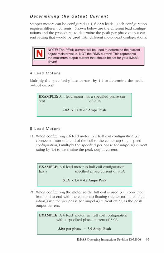
Stepper motors can be configured as 4, 6 or 8 leads. Each configuration requires different currents. Shown below are the different lead configu-rations and the procedures to determine the peak per phase output cur-rent setting that would be used with different motor/lead configurations.
4 L e a d Mo t o r s
Multiply the specified phase current by 1.4 to determine the peak output current.
6 L e a d Mo t o r s
1) When configuring a 6 lead motor in a half coil configuration (i.e. connected from one end of the coil to the center tap (high speed configuration)) multiply the specified per phase (or unipolar) current rating by 1.4 to determine the peak output current.
2) When configuring the motor so the full coil is used (i.e. connected from end-to-end with the center tap floating (higher torque configu-ration)) use the per phase (or unipolar) current rating as the peak output current.
NOTE! The PEAK current will be used to determine the current adjust resistor value, NOT the RMS current! This represents the maximum output current that should be set for your IM483 driver!
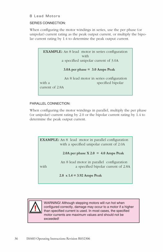
36 IM483 Operating Instructions Revision R032306 37IM483 Operating Instructions Revision R032306
EXAMPLE: An 8 lead motor in series configuration with
a specified unipolar current of 3.0A
3.0A per phase = 3.0 Amps Peak
An 8 lead motor in series configuration with a specified bipolar current of 2.8A
8 L e a d Mo t o r s
SERIES CONNECTION:
When configuring the motor windings in series, use the per phase (or unipolar) current rating as the peak output current, or multiply the bipo-lar current rating by 1.4 to determine the peak output current.
PARALLEL CONNECTION:
When configuring the motor windings in parallel, multiply the per phase (or unipolar) current rating by 2.0 or the bipolar current rating by 1.4 to determine the peak output current.
EXAMPLE: An 8 lead motor in parallel configuration with a specified unipolar current of 2.0A
2.0A per phase X 2.0 = 4.0 Amps Peak
An 8 lead motor in parallel configuration with a specified bipolar current of 2.8A
2.8 x 1.4 = 3.92 Amps Peak
WARNING! Although stepping motors will run hot when configured correctly, damage may occur to a motor if a higher than specified current is used. In most cases, the specified motor currents are maximum values and should not be exceeded!

36 IM483 Operating Instructions Revision R032306 37IM483 Operating Instructions Revision R032306
Se t t i n g t h e Ou t p u t C u r r e n t
The IM483 uses an internal 1 milliamp current source to establish the reference voltage needed to control the output current. This voltage is programmed by means of an external 1/8 watt or higher, 1 percent resis-tor connected between P2:2 (Current Adjust) and P2:3 (Power Ground).
The relationship between the output current and the current adjust resis-tor value is expressed as follows:
Output Current = .002 X Resistor Value (Ω)
Figure 7.2 illustrates the connection of this resistor. Table 7.1 lists the resistor values for the driver output current in 200 milliamp increments.
NOTE: Resistor leads shouldbe as short as possible tominimize the amount of noisecoupled into the driver!
P2
P2:2P2:3
Driver Output Current =.002 X Resistor Value ( )
Current Adjust Resistor1/8 W 1%
Figure 7.2: Current Adjust Resistor Placement
seulaVrotsiseRtsujdAtnerruC384MI
tnerruCtuptuO)kaePspmA(
eulaVrotsiseR)%1smhO(
tnerruCtuptuO)kaePspmA(
eulaVrotsiseR)%1smhO(
4.0 002 4.2 0121
6.0 103 6.2 0031
8.0 293 8.2 0041
0.1 994 0.3 0051
2.1 095 2.3 0851
4.1 896 4.3 0961
6.1 787 6.3 0871
8.1 788 8.3 0191
0.2 0001 0.4 0002
2.2 0011 - -
Table 7.1: Current Adjust Resistor Values
WARNING! Do not operate the IM483 Driver without a Current
Adjustment Resistor!
A resistor MUST be placed between the Current Adjust Input (Pin 2
on P2) and ground (Pin 3 on P2) to keep the IM483 Driver and/or

38 IM483 Operating Instructions Revision R032306 39IM483 Operating Instructions Revision R032306
Redu c i n g/D i s a b l i n g t h e Ou t p u t C u r r e n t
The IM483 has the capability of automatically reducing the current in the motor windings following a move. Use of this feature will reduce motor and driver heating, thus allowing for cooler operation and improved system power efficiency.
The output current may be reduced to the level needed to maintain mo-tor holding torque by means of a 1/8 watt or higher, 1 percent resistor. This resistor is connected between P2:1 (Reduction Adjust) and P2:2 (Current Adjust). The value of the reduced output current will also be de-pendant on the current adjust resistor value as expressed in the equation below. Figure 7.3 illustrates the connection. If no resistor is placed, the current in the motor windings will be at the amount set by the current adjust resistor when the motor is stopped and the driver enabled.
To reduce the current in the motor windings to zero between moves, the drive may be disabled by pulling the enable/disable input (P1:5) to ground by means of a sinking output on your controller or PLC, or by placing a shunt between pins 1 and 2 of connector P2. Note that if the controller continues to send step clock pulses to the driver, the internal counter on the IM2000 controller ASIC will continue to increment unless the driver is reset. This will only affect your system if the On-Full-Step output is used for position monitoring.
The amount of current reduced will depend upon the value of the re-
duction adjust resistor (RRed
) and the value of the current adjust resistor
(RAdj
). The current will be reduced aproximately 1.0 seconds after the
rising edge of the last step clock pulse. The value of RRed
is calculated as follows:
IRun
is the desired peak running current. Range 0.4A to 4A Peak
IHold
is the desired peak holding current. Range 0.2A to 4A Peak
IRun x IHoldRRed = 500 x ( IRun - IHold)
NOTE: Resistor leads shouldbe as short as possible tominimize the amount of noisecoupled into the driver!
P2
P2:1
P2:2Current Adjust Resistor
1/8 W 1%
Reduction Adjust Resistor1/8 W 1%
Figure 7.3: Current Reduction Adjust Resistor Placement

38 IM483 Operating Instructions Revision R032306 39IM483 Operating Instructions Revision R032306
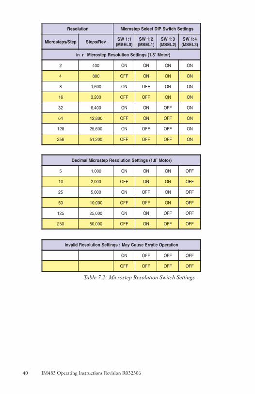
Con t r o l l i n g t h e Ou t p u t R e s o l u t i o n
The number of microsteps per step is selected by the DIP switch (SW1). Table 7.2 lists the standard resolution values along with the associated switch settings for a 1.8° stepping motor.
If a motor with a different step angle is used, then the steps per revolu-tion resolution will have to be calculated manually by multiplying the microsteps/step setting by the number of full steps per motor revolution.
For example, a 0.45° step angle motor (800 Fullsteps/Rev) set to 16 microsteps/step will have a resolution of 12,800 steps/rev.
These settings may be switched on-the-fly. There is no need to reset or disable the drive in order to change the output resolution. The resolution change will occur upon the rising edge of the step clock pulse following the change.
If remote control of the output resolution is required, these signals are brought out on connector P1 on the IM483-34P1. This option is discussed in detail in Appendix A: Standard Connector Options.
NOTE! The table and example settings are for a stepper motor with 1.8° step angle. If using a motor with a different step angle the steps/rev resolution will vary with the step angle.
Figure 7.4: MSEL Switch Showing 50 Microsteps/Step Selected
MSEL0MSEL1MSEL2MSEL3
ON
SW1
P1
40 IM483 Operating Instructions Revision R032306 41IM483 Operating Instructions Revision R032306
Table 7.2: Microstep Resolution Switch Settings

40 IM483 Operating Instructions Revision R032306 41IM483 Operating Instructions Revision R032306
I n t e r f a c i n g a n d U s i n g t h e I s o l a t e d L o g i c I n p u t s
The IM483 has 4 optically isolated logic inputs which are located on connector P1. These inputs are isolated to minimize or eliminate electri-cal noise coupled onto the drive control signals. Each input is internally pulled-up to the level of the optocoupler supply and may be connected to sinking outputs on a controller such as the IMS LYNX or a PLC. These inputs are:
1] Step Clock (P1:2)2] Direction (P1:3)3] Enable (P1:5)4] Reset (P1:6)
Of these inputs only step clock and direction are required to operate the IM483.
The schematic shown in Figure 7.5 illustrates the inputs.
HP-2630
HP-2630
HP-2630
HP-2630
470W
470W
470W
470W
Optocoupler Supply P1:4+5VDC
Step Clock P1:2
CW/CCW Direction P1:3
Enable/Disable P1:5
Reset P1:6
Figure 7.5: Optically Isolated Inputs

42 IM483 Operating Instructions Revision R032306 43IM483 Operating Instructions Revision R032306
Powe r i n g t h e Op t o c o up l e r s
In order to maintain isolation, the optocouplers must be powered by an external power supply connected to P1:4, with the opto supply ground connected to the ground of the input control circuitry. The logic inputs are internally limited to allow for a +5VDC power supply.
A power supply in excess of +5 volts may be used, however a current limiting resistor MUST be placed in series with the input to limit the input forward current to the recommended 7 milliamps. At no time can the input forward current exceed 15 milliamps or damage may occur to
WARNING! The isolated logic inputs on the IM483 are internally limited to allow for an optocoupler supply voltage of +5 VDC. If using a higher voltage supply, a current limiting resistor must be placed in series with the input or damage will occur to the IM483’s input circuitry, rendering the drive
Table 7.3: Recommended Input Current Limiting Resistor Values
srotsiseRgnitimiLtnerruCtupnIdetalosI
ylppuSotpO)CDV+(
eulaVrotsiseR)%5smhO(
eulaVrotsiseR)%1smhO(
5 - -
01 086 186
21 0001 0001
51 0031 0031
42 0072 0762
I s o l a t e d L o g i c I n p u t C h a r a c t e r i s t i c s
S t e p C l o c k ( P1 :2 )
The step clock input is where the motion clock from your control circuit-ry will be connected. A positive going edge on this input will increment or decrement the sine/cosine position generator in the IM2000 ASIC. The size of this increment or decrement will depend on the microstep resolu-tion setting. The motor will advance one microstep in the plus or minus direction (based upon the state of the direction input) on the rising edge of each clock pulse.
The positive going edge of this input will also update and latch the states of the direction and microstep select inputs. If no change has occured to these inputs then the drive will make the next step.
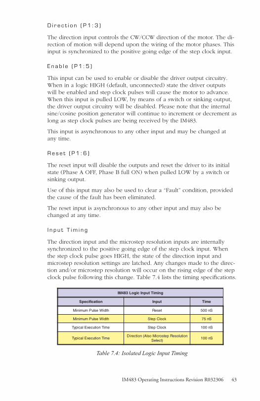
42 IM483 Operating Instructions Revision R032306 43IM483 Operating Instructions Revision R032306
D i r e c t i o n ( P1 :3 )
The direction input controls the CW/CCW direction of the motor. The di-rection of motion will depend upon the wiring of the motor phases. This input is synchronized to the positive going edge of the step clock input.
E n a b l e ( P1 :5 )
This input can be used to enable or disable the driver output circuitry. When in a logic HIGH (default, unconnected) state the driver outputs will be enabled and step clock pulses will cause the motor to advance. When this input is pulled LOW, by means of a switch or sinking output, the driver output circuitry will be disabled. Please note that the internal sine/cosine position generator will continue to increment or decrement as long as step clock pulses are being received by the IM483.
This input is asynchronous to any other input and may be changed at any time.
Rese t ( P1 :6 )
The reset input will disable the outputs and reset the driver to its initial state (Phase A OFF, Phase B full ON) when pulled LOW by a switch or sinking output.
Use of this input may also be used to clear a “Fault” condition, provided the cause of the fault has been eliminated.
The reset input is asynchronous to any other input and may also be changed at any time.
I n p u t T im i n g
The direction input and the microstep resolution inputs are internally synchronized to the positive going edge of the step clock input. When the step clock pulse goes HIGH, the state of the direction input and microstep resolution settings are latched. Any changes made to the direc-tion and/or microstep resolution will occur on the rising edge of the step clock pulse following this change. Table 7.4 lists the timing specifications.
gnimiTtupnIcigoL384MI
noitacificepS tupnI emiT
htdiWesluPmuminiM teseR Sn005
htdiWesluPmuminiM kcolCpetS Sn57
emiTnoitucexElacipyT kcolCpetS Sn001
emiTnoitucexElacipyTnoituloseRpetsorciMoslA(noitceriD
)tceleSSn001
Table 7.4: Isolated Logic Input Timing

44 IM483 Operating Instructions Revision R032306 45IM483 Operating Instructions Revision R032306
I n t e r f a c e Me t h o d s
The isolated logic inputs may be interfaced to the user’s control system in a variety of ways. In all cases the inputs are normally in a logic HIGH state when left floating. For purposes of this manual we will show three interface methods:
1] Switch Interface.2] Open Collector Interface.3] TTL Interface.
We will also show IM483 inputs connected to the IMS LYNX modular mo-tion controller, which is a powerful machine control soulution.
Sw i t c h I n t e r f a c e
A switch connected between the input and the opto supply ground will sink the input. If this method is used a SPST (Single-Pole, Single-Throw) switch works well for enable and direction. A normally-open momentary switch works well for reset. Figure 7.6 illustrates a SPST switch connected to the direction input.
MSEL0MSEL1MSEL2MSEL3
ON
SW1
P1
Direction P1:3
Opto Supply P1:4
+5 VDCOpto Supply
+
GND
Figure 7.6: Switch Interface
44 IM483 Operating Instructions Revision R032306 45IM483 Operating Instructions Revision R032306
MSEL0MSEL1MSEL2MSEL3
ON
SW1
P1+VDC
CONTROLLEROUTPUT R
1⁄4 W 1%LIMIT
+VDC
510121524
-----681100013002670
RLIMIT
Opto Supply P1:4
Reset P1:6
Low PulseWill ResetDriver
Open C o l l e c t o r I n t e r f a c e
Figure 7.7 shows an open collector interface connected to the reset input. This interface method may be used with any of the logic inputs. Remem-ber that a current limiting resistor is required if an opto supply voltage greater than +5 VDC is used.
Figure 7.7: Open Collector Interface
TT L I n t e r f a c e
Figure 7.8 shows a TTL device connected to the enable input. This inter-face method may be used with any of the logic inputs.
Figure 7.8: TTL Interface
MSEL0MSEL1MSEL2MSEL3
ON
SW1
P1
+5 VDC
CONTROLLEROUTPUT
Opto Supply P1:4
Enable P1:5

46 IM483 Operating Instructions Revision R032306 47IM483 Operating Instructions Revision R032306
IM483 I n t e r f a c e d t o a n IMS LYNX
The LYNX Controller is a powerful, machine control solution which can be used to meet the system design needs of a wide range of applications. It has the capability of controlling up to three axes sequentially when used with the optional high speed differential I/O module. For more information on the LYNX, brows
e the IMS web site at www.imshome.com.
Figure 7.9 shows a LYNX Control Module and Differential I/O Module providing step clock, direction and optocoupler supply voltage to two IM483 drivers. The LYNX isolated I/O may also be used to control the enable and reset inputs, the MSEL inputs (IM483-34P1) and receive feed-back from the fault and fullstep outputs.
IM483 Driver #1
IM483 Driver #2
+5VDC Opto Supply
+5VDCOpto Supply
Step Clock InputDirection Input
SCLK+DIR+
+5VDCOUTPUT
DIR+
DIR-
SCK-
SCK+
GND
+5V
RX-
RX+
TX-
TX+
CGND
RX
TX
22
21
23
24
25
26
31
32
33
34
35
36
IG
INTELLIGENT MOTION SYSTEMS, INC.FAULT
POWER
12
34
56 1
23
45
61
23
45
6
2221
23242526
313233343536
GND
V+
A1A0
A2PTHIUG
TM
Differential/OM
ODULE
TM
13+
13-
14-
14+
15-
15+
16-
16+
17-
17+
18-
18+
GD
SteppingMotor #2
N Power ConnectionsNot Shown ForSimplification
MSEL0MSEL1MSEL2MSEL3
ON
SW1
P1 P2
MSEL0MSEL1MSEL2MSEL3
ON
SW1
P1 P2
SteppingMotor #1
HSI/O Drive #2
13+ Step Clock
14+ Direction
Figure 7.9: LYNX Interface

46 IM483 Operating Instructions Revision R032306 47IM483 Operating Instructions Revision R032306
Conne c t i n g a n d U s i n g t h e F a u l t O u t p u t
The IM483 has an open collector fault output located on P1:7. This output is non-isolated and has the ability of sustaining maximum driver voltage. It can sink a maximum of 25mA, which is sufficient to drive an LED or a small relay.
This output is active when in a LOW state. The following conditions will cause this output to become active:
1] Phase-to-phase short circuit.2] Phase-to-ground short circuit.3] Phase over-current condition.
When the fault output becomes active, it disables the driver outputs and latches in this condition. It can only be cleared by toggling the reset input LOW, or by powering OFF then powering ON the drive.
Figure 7:10 illustrates the fault output connected to an LED.
Fault Output P1:7
LED
Current LimitingResistor
P2:4 +V (+12 to +48VDC)
MSEL0MSEL1MSEL2MSEL3
ON
SW1
P1 P2
Figure 7.10: The Fault Output Connected to an LED
NOTE! Once the fault output is active, it can only be cleared by toggling the reset input LOW, or by powering off the driver.
NOTE! The IM483 driver outputs will disable in the event of an over-temperature condition, however, in this case the fault output WILL NOT latch. The driver will begin operating again when the temperature drops below the shut-off threshold.

48 IM483 Operating Instructions Revision R032306 49IM483 Operating Instructions Revision R032306
Fu l l S t e p Ou t p u t
The full step output is a high speed MOSFET (open drain) output located at P1:8. This output will toggle LOW each time the driver makes a full step, and remain so for the duration of the full step. A full step occurs each time the Phase A or Phase B sine wave crosses through zero. At zero crossing there will be full current in one motor winding, zero current in the other. This full step position is a common position regardless of the microstep resolution selected.
This high speed output is non-isolated and can sustain maximum driver volt-age. It is capable of sinking up to 25mA.
This output can be used to count the number of full steps directed by the driver. By so utilizing this output, the user can both measure the repeatability of the stepper system and track motor position. Please note that using this output is not closed-loop control, merely a method of monitoring position and repeatability. It represents full steps commanded by the driver, not actual full steps moved by the motor.
The application example shown in figure 7.11 illustrates a method where an up/down counter may be connected to the full step output. The counter will count the number of full steps up or down based upon the state of the direction input. The count input of the counter will increment or decrement with each full step taken.
As noted in the drawing, this is only a representation of a possible application of the full step output. Additional interface circuitry may be required between the IM483 and the counter. Check the documentation provided by the manu-facturer of your counter for interface requirements.
Figure 7.11: The Full Step Output Connected to an Up/Down Counter
Full Step Output P1:8
+VDC
Opto SupplyP1:4
Direction P1:3
Up/Down
Count
ControllerOutput
Up/Down Counter
NOTE: This drawing represents a possible applicationof the full step output. Additional interface circuitrymay be required between the IM483 and the counter!
MSEL0MSEL1MSEL2MSEL3
ON
SW1
P1 P2

48 IM483 Operating Instructions Revision R032306 49IM483 Operating Instructions Revision R032306
Min imum Conn e c t i o n s
The following figure illustrates the minimum connection requirements for the IM483.
+5 VDCOpto
Supply
Step ClockOscillator
Direction
Current AdjustmentResistor
ØAØAØBØB
Step Clock
P1:1
P2:1
TORQUE:Maximum torque on terminal screws is 4.5 lbs-in (0.5 N-m). DO NOT Overtighten !
SUPPLY AND MOTOR WIRING:Use 18 AWG twisted pair.(Belden #9740 or equivalent)
Figure 7.12:IM483 Minimum Required Connections

50 IM483 Operating Instructions Revision R032306 51IM483 Operating Instructions Revision R032306
Sec tion 8Tr o u b l e s h o o t i n g
Se c t i o n O v e r v i ew
This section will cover the following:
n Basic Troubleshooting.
n Common Problems/Solutions.
n Contacting Technical Support.
n Product Return Procedure.
n 24-Month Limited Warranty.
Bas i c Tr o u b l e s h o o t i n g
In the event that your IM483 doesn’t operate properly, the first step is to identify whether the problem is electrical or mechanical in nature. The next step is to isolate the system component that is causing the prob-lem. As part of this process you may have to disconnect the individual components that make up your system and verify that they operate inde-pendently. It is important to document each step in the troubleshooting process. You may need this documentation to refer back to at a later date, and these details will greatly assist our Technical Support staff in determining the problem should you need assistance.
Many of the problems that affect motion control systems can be traced to electrical noise, controller software errors, or mistakes in wiring.
P r ob l em S ymp t oms a n d P o s s i b l e C a u s e s
• S ymp t om
Motor does not move.
• P o s s i b l e P r o b l em
No power.
Unit is in a reset condition.
Invalid microstep resolution select setting.

50 IM483 Operating Instructions Revision R032306 51IM483 Operating Instructions Revision R032306
Current adjust resistor is wrong value or not in place.
Fault condition exists.
Unit is disabled.
Motor moves in the wrong direction.
• P o s s i b l e P r o b l em
Motor phases may be connected in reverse.
• S ymp t om
Unit in fault.
• P o s s i b l e P r o b l em
Current adjust resistor is incorrect value or not in place.
Motor phase winding shorted.
Power input or output driver electrically overstressed.
• S ymp t om
Erratic motor motion.
• P o s s i b l e P r o b l em
Motor or power wiring unshielded or not twisted pair.
Logic wiring next to motor/power wiring.
Ground loop in system.
Open winding of motor.
Phase bad on drive.
Invalid microstep resolution select setting.
• S ymp t om
Motor stalls during acceleration.
• P o s s i b l e P r o b l em
Incorrect current adjust setting or resistor value.
Motor is undersized for application.
Acceleration on controller is set too high.
Power supply voltage too low.

52 IM483 Operating Instructions Revision R032306 53IM483 Operating Instructions Revision R032306
• S ymp t om
Excessive motor and driver heating.
• P o s s i b l e P r o b l em
Inadequate heat sinking / cooling.
Current reduction not being utilized.
Current set too high.
• S ymp t om
Inadequate holding torque.
• P o s s i b l e P r o b l em
Incorrect current adjust setting or resistor value.
Increase holding current with the current reduction adjust resistor.

52 IM483 Operating Instructions Revision R032306 53IM483 Operating Instructions Revision R032306
Th e IMS Web S i t e
Another product support resource is the IMS web site located at http://www.imshome.com. This site is updated monthly with tech tips, applica-tions and new product updates.
Re t u r n i n g Yo u r P r o d u c t t o IMS
If Technical Support determines that your IM483 needs to be returned to the factory for repair or replacement, you will need to take the following steps:
n Obtain an RMA (Returned Material Authorization) number and shipping instructions from Customer Service.
n Fill out the “Reported Problem” field in detail on the RMA form that Customer Service will fax you.
n Enclose the product being returned, and the RMA form in the box. Package product in its original container if possible. If original packaging is unavailable ensure that the product is enclosed in approved antistatic packing material. Write the RMA number on the box.
The normal repair lead time is 10 business days. Should you need your product returned in a shorter time period, you may request that a “HOT” status be placed upon it while obtaining an RMA number. Should the fac-tory determine that the product repair is not covered under warranty, you will be notified of any charges.
Con t a c t i n g Te c h n i c a l S u p p o r t
In the event that you are unable to isolate the problem with your IM483, the first action you should take is to contact the distributor from whom you originally purchased your product or IMS Technical Support at 860-295-6102 or by fax at 860-295-6107. Be prepared to answer the following questions:
n What is the application?
n In detail, how is the system configured?
n What is the system environment? (Temperature, Humidity, Exposure to chemical vapors, etc.)
n What external equipment is the system interfaced to?

54 IM483 Operating Instructions Revision R032306 55IM483 Operating Instructions Revision R032306
A p p en dix AS t a nda r d C onn e c t i o n Op t i o n s
Append i x O v e r v i ew
The IM483 has multiple connection options available to the user. In gen-eral, these options will not change the operational characteristics of the driver. These connector options give the user multiple choices in how to interface and mount the driver into a system. Listed below are the con-nector options and how they may be used.
IM483 -34P1
The IM483-34P1 features the standard 8 pin terminal block at the connec-tor P2 location. P1 has been replaced by a 34 pin header.
The typical use for this connector style is remote control of the micro-step resolution select inputs. The advantages of this control method are discussed later in this appendix.
IM483 -8P2
This connector option uses 8 - 0.045 square pins at the P2 connector location. The P1 connector location uses 8 -0.025 square pins.
This connector style would be advantageous in a scenario where the user desires to either solder or plug the IM483 directly into a system PCB. Dimen-sions and PCB hole patterns are given later in this appendix.
IM483 -34P1 -8P2
This option combines the features and potential uses of the IM483-34P1 and the IM483-8P2.
IM483 - P LG
The IM483-PLG replaces both connectors P1 and P2 with an Altech 8 position pluggable interface. The removeable, plug-in screw terminal set is available as an option (PLG-R).
This connector option is useful in system designs where ease of removal is desired. For example, the IM483-PLG is pin compatible with the IM804/5-PLG. If more power is needed the drives are easily swapped.

54 IM483 Operating Instructions Revision R032306 55IM483 Operating Instructions Revision R032306
IM483 -34P1
The IM483-34P1 connector configu-ration replaces the 8 position screw terminal at connector location P1 with a 34 pin header. Connector P2 is still an 8 position screw terminal.
There are 2 key features that are added with this connector option:
1] Microstep resolution select inputs (MSEL) on P1 allow for remote control of the output resolution.
2] Step/Direction outputs follow the step/direction inputs, allow-ing for multiple drives to be cascaded.
0.100(2.54)
0.100(2.54)
8X 0.025 (0.64)Sq. PostTin Plated Bronze
Applicable Products:IM483-34P1
34 Pin Connector Pins - P1
0.230(5.84)
0.510(12.95)
Figure A.1: IM483-34P1 Connector P1 Mechanical Drawing
MSEL0MSEL1MSEL2MSEL3
ON
SW1P1 P2
Pin 1
Pin 17
Pin 18
Pin 34
Figure A.2: IM483-34P1Connector P1Pin Locations
P i n C o n f i g u r a t i o n / De s c r i p t i o n
Figure A.2 and Table A.1 show the pin location and description of the 34 pin

56 IM483 Operating Instructions Revision R032306 57IM483 Operating Instructions Revision R032306
Table A.1: IM483-34P1 Connector P1Pin Assignment and Description
C1P43-384MI noitarugifnoC1Protcenno
#NIP NOITCNUF SLIATED
3 3tceleSnoituloseR .tupnI3tceleSnoituloseRpetsorciM
4 tupnIkcolCpetSrotomehtsecnavdatupnisihtnoegdegniogevitisopA
tnednepedsitnemercniehtfoezisehT.tnemercnieno.1WShctiwstcelesnoituloserehtfosgnittesehtnopu
6 tupnInoitceriD.rotomehtfonoitceridehtegnahcotdesusitupnisihTfonoitcennocehtnopusdnepedoslanoitceridlacisyhP
.sgnidniwrotomeht
8 ylppuSotpOdetalosiehtotrewopylppusotdesusitupniCDV5+sihTtsumeractub,desuebyamegatlovrehgihA.stupnicigol
.relpuoc-otpoehthguorhttnerrucehttimilotnekateb
01 elbasiD/elbanEtupnI
fonoitcestuptuoehtelbasid/elbaneotdesusitupnisihTeht,)nepo(etatsHGIHcigoLaninehW.revirdeht
tibihnitonseodtupnisiht,revewoH.delbaneerastuptuoehtybetadpulliwstuptuoeht,erofereht,kcolcpetseht
elihwrevirdehtotdeilppa)ynafi(seslupkcolcforebmun.delbasidsawti
21 tupnIteseRstuptuoesahp(revirdehtteserlliwtupnisiht,WOLnehW
laitinistitaeblliwrevirdeht,desaelernehW.)elbasidlliw.)NOBesahP,FFOAesahP(etats
41 tuptuOtluaFsahnoitidnoctiucrictrohsatahtsetacidnituptuosihT
.WOLevitcasituptuosihT.derrucco
62,61 tuptuOpetS-lluF-nO
sirevirdehtnehwsetacidnituptuorotcellocneposihTtnuocotdesuebnactuptuosihT.petslluftadenoitisop
sseldrager,devomsahrotomehtspetsllufforebmunehtsituptuosihT.neewtebnispetsorcimforebmunehtfo
.WOLevitca
12 tuptuOkcolCpetS .tupnipetsswolloftuptuokcolcpetsdetalosi-noN
22 tuptuOnoitceriD .tupninoitceridswolloftuptuonoitceriddetalosi-noN
32 0tceleSnoituloseR .tupnI0tceleSnoituloseRpetsorciM
42 2tceleSnoituloseR .tupnI2tceleSnoituloseRpetsorciM
52 1tceleSnoituloseR .tupnI1tceleSnoituloseRpetsorciM
72 dnuorG .dnuorgrewophtiwnommoC.dnuorgdetalosi-noN
:ETON tcennoconera43-82dna,02,91,81,71,51,31,11,9,7,5,2,1srebmunniP.elbatsihtmorfdetimmoneebevahsuht)C/N(snip

56 IM483 Operating Instructions Revision R032306 57IM483 Operating Instructions Revision R032306
Th e R e s o l u t i o n S e l e c t (MSEL ) I n p u t s
One of the key features of the 34 pin header is the availability of the res-olution select inputs on P1. This allows the user to take external control of the driver output resolution, enabling the user to switch the output resolution “on-the-fly”.
An example would be to switch to a lower resolution (higher velocity, lower positional accuracy) during a long move. When the move nears completion, switch back to a higher resolution (lower speed, greater positional accuracy) to accurately position the axis. This on-the-fly “gear shifting” facilitates high speed slewing combined with high resolution positioning at either end of the move.
The microstep resolution is synchronized with the step clock input. If the resolution change does not fall on a full step, the IM483 will readjust itself at the next pulse that would overshoot the fullstep position. This feature allows the IM483 to readjust the motor position regardless of the output resolution selected during a resolution change.
These inputs are non-isolated and are active when in a logic LOW state (if left open or floating the input is considered to be OFF). They are pulled-up to +5 VDC via 1.5 kΩ resistors. These inputs may to be inter-faced via an external switch or sinking output on a control device. Figure A.3 shows the resolution select inputs connected using a TTL interface method. Note that the DIP switch (SW1) is still in place and may be used to control the resolution. If controlling the resolution externally, the four switches need to be in the “OFF” position.
The driver output resolution has two modes of operation: decimal and binary. The modes are switched by changing the logic state of MSEL 3. If MSEL 3 is in a logic HIGH (open/floating) state the output resolution will be in decimal mode. Binary mode is entered by sinking MSEL 3 to a 0 state.
Typically, in cases where resolution is being switched on-the-fly, only one mode will be used. The desired mode may be selected by position-ing the DIP switch (SW1:4) for MSEL 3 to the appropriate state for the selected mode, then the resolution may be controlled by changing the states of MSEL 0 - 2 as needed, thus using only 3 outputs on the control device.
NOTE! When controlling the driver output resolution externally, the DIP switches (SW1) should be in the “OFF” position.
58 IM483 Operating Instructions Revision R032306 59IM483 Operating Instructions Revision R032306
Figure A.3: MSEL Connection Using TTL Interface

58 IM483 Operating Instructions Revision R032306 59IM483 Operating Instructions Revision R032306
+5 VDC
Step ClockOscillator
Direction Input
Direction In
Direction Out
Step Clock Input
Step Clock InP1:4
P1:6
P1:8
Step Clock Out
P1:8
+P1:27
P1:27
GND
GND
GND
Note: Optical isolation is defeated as shown in this diagram.
S t e p C l o c k a n d D i r e c t i o n O u t p u t s
Another key feature offered by the IM483-34P1 is the non-isolated step clock and direction outputs. These outputs will follow the step and direction inputs. This allows for multiple drives to be cascaded, with the primary drive receiving the step/direction signals from the control device, and the drives connected to the step/direction outputs to follow the primary. Figure A.4 illustrates a possible connection/application of these outputs.
These outputs used in this configuration would allow the user to elec-tronically gear or ratio the drives using the MSEL inputs. For instance, if the resolution of the primary drive was set to 128 and the secondary drive set to 256, when a move is commanded, the secondary drive will move 1/2 the distance and velocity of the primary drive.
Figure A.4: Cascading IM483-34P1 Drives Using the Step/Direction Outputs
Op t i o na l S c r ew Te rm i na l I n t e r f a c e f o r P1
The BB-34-4P is an optional breakout board that plugs directly into the pin receptacle for P1. This gives the user a screw terminal interface to P1. For drawings and details please see Appendix D: Accessories, BB-34-4P.
60 IM483 Operating Instructions Revision R032306 61IM483 Operating Instructions Revision R032306
IM483 -8P2
This connector option uses 8 - 0.045 square pins at the P2 connector location. The P1 connector location uses 8 -0.025 square pins.
This connector style is advantageous in a scenario where the user desires to either solder the IM483 directly into a system PCB or wire-wrap the interface connections. Figures A.5 and A.6 show the pin dimensions.
0.720(18.29)
0.820(20.83)
0.200(5.08)
8X 0.025 (0.64)Sq. PostTin Plated Bronze
Applicable Products:IM483-8P2
8 Pin Connector Pins - P1
Figure A.5: IM483-8P2 - Connector P1
0.720(18.29)
0.820(20.83)
0.200(5.08)
8X 0.025 (0.64)Sq. PostTin Plated Bronze
Applicable Products:IM483-8P2
8 Pin Connector Pins - P1
Figure A6: IM483-8P2 - Connector P2
60 IM483 Operating Instructions Revision R032306 61IM483 Operating Instructions Revision R032306
PCB Ho l e P a t t e r n
The IM483-8P2 is ideal for solder-mounting into a user’s PC board design. Figure A.7 illustrates the PCB hole pattern as well as the recommended hole and pad diameter for the IM483-8P2.
Figure A.7: IM483-8P2 PCB Hole Pattern
Recommended S o l d e r i n g P r a c t i c e s
The following practices are recommended when solder mounting the IM483-8P2 into your PCB:
Recommended S o l d e r Tempe r a t u r e
n 315°C (600°F)
Recommended S o l d e r T ime
n 10 Seconds
Recommended S o l d e r s
n Kester “245” No-clean core solder.n Alpha Metals “Telecore Plus Solder.n Multicore “X39B” No-clean Solder.n Or equivalent.
Recommended S o l v e n t
n Tech Spray “Envirotech 1679”.n Chemtronics “Flux-off NR 2000”.n Or equivalent.
0.200(5.08)
2.400(60.96)
Hole: 8X Ø 0.041 ( 1.04) ThruPad: 8X Ø 0.082 (2.08)
Hole: 8X Ø 0.069 (1.75) ThruPad: 8X Ø 0.138 (3.50)
0.200(5.08)

62 IM483 Operating Instructions Revision R032306 63IM483 Operating Instructions Revision R032306
IM483 -34P1 -8P2
This option combines the features and potential uses of the IM483-34P1 and the IM483-8P2. The connec-tor pins used for connector P2 are identical to those used on the IM483-8P2. The difference between the P1 connector on this model and the standard IM483-34P1 is in the pin height of the pin header shipped with the drive. There is no difference in the receptacle used.
This option may be solder-mount-ed or the pins may be wire-wrapped for interfacing.
0.811(20.62)
0.914(23.16)
0.200(5.08)
8X 0.045 (1.14)Sq. PostTin Plated Bronze
Applicable Products:IM483-8P2IM483-34P1-8P2
8 Pin Connector Pins - P2
0.520(13.21)0.800
(20.32)
0.100(2.54)
0.100(2.54)
8X 0.025 (0.64)Sq. PostTin Plated Bronze
Applicable Products:IM483-34P1-8P2
34 Pin Connector Pins - P1
Figure A.8: IM483-34P1-8P2 - Connector P1
Figure A9: IM483-34P1-8P2 - Connector P2

62 IM483 Operating Instructions Revision R032306 63IM483 Operating Instructions Revision R032306
PCB Ho l e P a t t e r n
The IM483-34P1-8P2 is ideal for solder-mounting into a user’s PC board design. Figure A.10 illustrates the PCB hole pattern and recommended pad diameter for the IM483-8P2.
Figure A.10: IM483-34P1-8P2 PCB Hole Pattern
Recommended S o l d e r i n g P r a c t i c e s
The following practices are recommended when solder mounting the IM483-34P1-8P2 into your PCB:
Recommended S o l d e r Tempe r a t u r e
n 315°C (600°F)
Recommended S o l d e r T ime
n 10 Seconds
Recommended S o l d e r s
n Kester “245” No-clean core solder.n Alpha Metals “Telecore Plus Solder.n Multicore “X39B” No-clean Solder.n Or equivalent.
Recommended S o l v e n t
n Tech Spray “Envirotech 1679”.n Chemtronics “Flux-off NR 2000”.n Or equivalent.
0.200(5.08)
0.100
0.100
(2.54)
(2.54)
2.400(60.96)
Hole: 34X Ø 0.041 ( 1.04) ThruPad: 34X Ø 0.082 (2.08)
Hole: 8X Ø 0.069 (1.75) ThruPad: 8X Ø 0.138 (3.50)
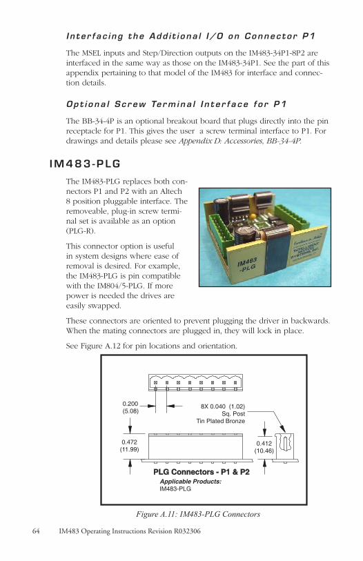
64 IM483 Operating Instructions Revision R032306 65IM483 Operating Instructions Revision R032306
I n t e r f ac i ng t he Add i t i ona l I /O on Connec to r P1
The MSEL inputs and Step/Direction outputs on the IM483-34P1-8P2 are interfaced in the same way as those on the IM483-34P1. See the part of this appendix pertaining to that model of the IM483 for interface and connec-tion details.
Op t i o na l S c r ew Te rm i na l I n t e r f a c e f o r P1
The BB-34-4P is an optional breakout board that plugs directly into the pin receptacle for P1. This gives the user a screw terminal interface to P1. For drawings and details please see Appendix D: Accessories, BB-34-4P.
IM483 -PLG
The IM483-PLG replaces both con-nectors P1 and P2 with an Altech 8 position pluggable interface. The removeable, plug-in screw termi-nal set is available as an option (PLG-R).
This connector option is useful in system designs where ease of removal is desired. For example, the IM483-PLG is pin compatible with the IM804/5-PLG. If more power is needed the drives are easily swapped.
These connectors are oriented to prevent plugging the driver in backwards. When the mating connectors are plugged in, they will lock in place.
See Figure A.12 for pin locations and orientation.
0.200(5.08)
0.472(11.99)
0.412(10.46)
Applicable Products:IM483-PLG
PLG Connectors - P1 & P2
8X 0.040 (1.02)Sq. Post
Tin Plated Bronze
Figure A.11: IM483-PLG Connectors

64 IM483 Operating Instructions Revision R032306 65IM483 Operating Instructions Revision R032306
12
34
56
78
87
65
43
21
Con
nect
orP
2
Con
nect
orP
1
MSEL0MSEL1MSEL2MSEL3
ON
SW1
P1 P2
Figure A.12: IM483-PLG Pin Location and Orientation
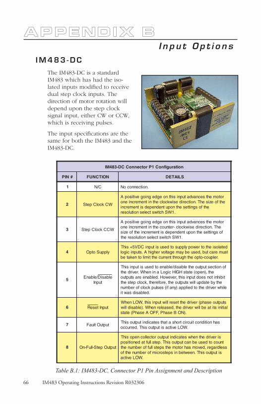
66 IM483 Operating Instructions Revision R032306 67IM483 Operating Instructions Revision R032306
A p p en dix BI n p u t O p t i o n s
IM483 -DC
The IM483-DC is a standard IM483 which has had the iso-lated inputs modified to receive dual step clock inputs. The direction of motor rotation will depend upon the step clock signal input, either CW or CCW, which is receiving pulses.
The input specifications are the same for both the IM483 and the IM483-DC.
Table B.1: IM483-DC, Connector P1 Pin Assignment and Description
CCD-384MI noitarugifnoC1Protcenno
#NIP NOITCNUF SLIATED
1 C/N .noitcennocoN
2 WCkcolCpetS
rotomehtsecnavdatupnisihtnoegdegniogevitisopAehtfoezisehT.noitceridesiwkcolcehtnitnemercnieno
ehtfosgnittesehtnoputnednepedsitnemercni.1WShctiwstcelesnoituloser
3 WCCkcolCpetS
rotomehtsecnavdatupnisihtnoegdegniogevitisopAehT.noitceridesiwkcolc-retnuocehtnitnemercnieno
fosgnittesehtnoputnednepedsitnemercniehtfoezis.1WShctiwstcelesnoitulosereht
4 ylppuSotpOdetalosiehtotrewopylppusotdesusitupniCDV5+sihTtsumeractub,desuebyamegatlovrehgihA.stupnicigol
.relpuoc-otpoehthguorhttnerrucehttimilotnekateb
5 elbasiD/elbanEtupnI
fonoitcestuptuoehtelbasid/elbaneotdesusitupnisihTeht,)nepo(etatsHGIHcigoLaninehW.revirdeht
tibihnitonseodtupnisiht,revewoH.delbaneerastuptuoehtybetadpulliwstuptuoeht,erofereht,kcolcpetseht
elihwrevirdehtotdeilppa)ynafi(seslupkcolcforebmun.delbasidsawti
6 tupnIteseRstuptuoesahp(revirdehtteserlliwtupnisiht,WOLnehW
laitinistitaeblliwrevirdeht,desaelernehW.)elbasidlliw.)NOBesahP,FFOAesahP(etats
7 tuptuOtluaFsahnoitidnoctiucrictrohsatahtsetacidnituptuosihT
.WOLevitcasituptuosihT.derrucco
8 tuptuOpetS-lluF-nO
sirevirdehtnehwsetacidnituptuorotcellocneposihTtnuocotdesuebnactuptuosihT.petslluftadenoitisop
sseldrager,devomsahrotomehtspetsllufforebmunehtsituptuosihT.neewtebnispetsorcimforebmunehtfo
.WOLevitca
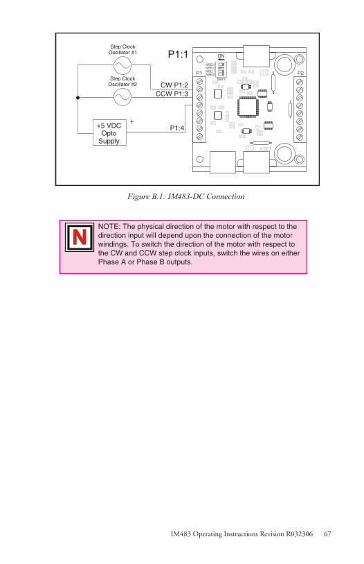
66 IM483 Operating Instructions Revision R032306 67IM483 Operating Instructions Revision R032306
Figure B.1: IM483-DC Connection
NOTE: The physical direction of the motor with respect to the direction input will depend upon the connection of the motor windings. To switch the direction of the motor with respect to the CW and CCW step clock inputs, switch the wires on either Phase A or Phase B outputs.
+5 VDCOpto
Supply
Step ClockOscillator #1
Step ClockOscillator #2 CW P1:2
CCW P1:3
P1:1
P1:4+

68 IM483 Operating Instructions Revision R032306 69IM483 Operating Instructions Revision R032306
A p p en dix CCoo l i n g S o l u t i o n s
H -4X Hea t S i n k K i t
The H-4X heat sink is designed for use with the IM483. When ordering, please specify which drive is being used as this heat sink is also used with the IB46X drivers. The H-4X comes with the following items:
(1) H-4X heat sink.(4) 6 X 32 mounting screws/washers.(1) TN-48 non-isolating thermal pad.
Mechan i c a l S p e c i f i c a t i o n s
6.00(152.4)
5.50(139.7)
3.15(80.1)
3.51(89.5)
6 X32 Threaded4 PLACES
0.85(21.6)
Figure C.1: H-4X Heat Sink, Dimensions in Inches (mm)
Th e r ma l Non - I s o l a t i n g P a d ( TN - 48 )
The TN-48 thermal non-isolating pad is a composite of .0015” (.038 mm) aluminum foil coated on both sides with a .0025” (.063 mm) thick thermally and electrically conductive rubber. These pads have a thermal conductivity of 0.65 W/m-K and a maximum temperature rating of 180°C.
One side of the TN-48 pad is adhesive and may be applied directly to the IM483 driver. The TN-48 pad eliminates the problems associated with using thermal grease.
This pad are also included in the heat sink kit.

68 IM483 Operating Instructions Revision R032306 69IM483 Operating Instructions Revision R032306
A p p en dix DAcc e s s o r i e s
Append i x O v e r v i ew
This appendix discusses in detail the optional accessories avalaible for use with the IM483. These accessories are:
n U3-CLP - Side-mounting clip set for all versions of the IM483.
n BB-34-4P - Breakout board for the -34P1 connection option.n PLG-R - Pluggable screw terminal set for use with the -PLG
connection option.
U3 -C LP : S i d e -Moun t i n g C l i p
The U3-CLP mounting clips were specially designed for the IM80X, IM483 series of Microstepping drivers and driver indexers and the ISP200 and ISP300 series power supplies to decrease overall panel space and allow for more flex-ible mounting patterns.
The 2 clips attach easily to the unit for optional side mounting and reduce the amount of panel space required to mount the drive by 42%. The low-profile clips attach to the side of the unit and do not interfere with various connection configurations.
I n c l u d e d i n t h e K i t
(1) IMS0063 Top Clip
(1) IMS0064 Bottom Clip
Recommended Ha r dwa r e (No t I n c l u d e d )
2 - 10 X 32 Pan Head Machine Screw (Length determined by mounting plate thickness)
2 - # 10 Lock Washers
3.36(85.34)
0.50(12.7)
Figure D1: U3-CLP Mounting Hole Locations

70 IM483 Operating Instructions Revision R032306 71IM483 Operating Instructions Revision R032306
Mounting Plate
#10 Hardware
U3-CLP
Unit Case. Componentsremoved for simplification.
Figure D.2: Attaching the U3-CLP to the IM483
Figure D.3: Mounting to a Panel
Mount i ng
The unit should be mounted in ac-cordance with Figure D.3 using the recommended hardware. Ensure that mounting hardware doesn’t in-terfere with any circuitry or wiring.
NOTE: The Mount-ing Clips MUST be placed on the side for which they are designed. They are
not interchangeable. They can, however, be attached to either vertical plate of the aluminum channel case.
WARNING! The maximum plate temperature for all the units that may be used with these
clips is 70°C. It may be nec-essary to install a fan in your enclosure or provide addi-tional heat sinking to remain below this temperature!
4 - # 10 Flat Washers
2 - 10 X 32 Nuts
I n s t a l l a t i o n
Using the photographs in Figure D.2, place the clips on the unit to be mounted as shown. The clips must be oriented in a fashion that places the smaller retaining tab between the bot-tom of the printed circuit board and the aluminum channel case

70 IM483 Operating Instructions Revision R032306 71IM483 Operating Instructions Revision R032306
BB -34 -4P Breakou t Board
The BB-34-4P breakout board is designed to provide a screw terminal interface for the IM483-34P1, IM483I, IM483IE and IM804/805-34P1 microstepping driver.
This interface is easily inserted into the P1 pin receptacle.
Mechan i ca l Spec i f i c a t i ons and W i r i ng Recommenda t i ons
IMS recommends that the following wiring practices be used to interface to the IM483-34P1 using the BB-34-4P:
n Wire Size: 16 - 22 AWGn Strip Length: 0.200” (5mm)n Screw Torque: 3.0 lb-in (0.33 N-m)
Mechanical specifications are illustrated in Figure D.4.
I n s ta l l a t i on
To install the BB-34-4P first remove the 34 pin header from the receptacle by gently rocking it back and forth and lifting the pin header straight upwards. Do not remove at a side-to-side angle.
Insert the breakout board into the P1 pin receptacle as shown in Figure D.6. Mount to drive and heat sink plate using the recommended mounting hardware.
Dimensions in Inches (mm)
2.635(66.92)2.441
(62.00)
1.050(26.67)
0.780(19.81)
0.107(2.72) 2X ØX 0.155
(2X ØX 3.94)
1
18
17
34
Figure D.4: BB-34-4P Mechanical Specifications

72 IM483 Operating Instructions Revision R032306 73IM483 Operating Instructions Revision R032306
IM483-34P1 CONNECTIONSSee Operating Instructions for Pin Description & Electrical Specifications
118
1734
Pin 1: N/CPin 2: N/CPin 3: MSEL 3Pin 4: Step Clock InputPin 5: N/CPin 6: Direction Input
Pin 8: Opto Supply
Pin 10: Enable Input
Pin 12: Reset Input
Pin 14: Fault Output
Pin 16: On-Full-Step Output
Pin 7: N/C
Pin 9: N/C
Pin 11: N/C
Pin 13: N/C
Pin 15: N/C
Pin 17: N/C
N/C: Pin 18N/C: Pin 19N/C: Pin 20
Step Clock Output: Pin 21Direction Output: Pin 22
MSEL 0: Pin 23
MSEL 1: Pin 25
Ground: Pin 27
N/C: Pin 29
N/C: Pin 31
N/C: Pin 33
MSEL 2: Pin 24
On-Full-Step Output: Pin 26
N/C: Pin 28
N/C: Pin 30
N/C: Pin 32
N/C: Pin 34
N/C = No Connection
Heat Sink Plate
Driver
BB-34-4P
Thermal PadIMS TN-48or Equivalent
Mounting Screw Torque:5.0 to 7.0 lb-in
(0.60 to 0.80 N-m)
Connector P1
A
B
C
Mounting Hardware - U.S.#6 Stainless Machine Screw#6 Split Lock Washer(.04 TH, .24 OD)#6 Flat Washer, Stainless(.04 TH, .24 OD)
A
B
C
Mounting Hardware - Metric#M3 Stainless Machine Screw#M3 Split Lock Washer(.08 TH, 6.20 OD)#M3 Flat Washer, Stainless(.05 TH, 6.20 OD)
A
B
C
Figure D.5: BB-34-4P Pin Locations
Figure D.6: BB-34-4P Mounting Diagram

72 IM483 Operating Instructions Revision R032306 73IM483 Operating Instructions Revision R032306
PLG -R R emo v ab l e S c r ew Te r m i n a l S e t
The PLG-R removable screw terminal set is the optional terminal set for the IM483-PLG connection configuration. Because the -PLG is configured to eliminate the possibility of plugging the driver in backwards, the kit includes two unique terminal blocks, one each for both P1 and P2.
Replacement terminals may be ordered individually as needed. The order num-bers for individual replacements are:
Connector P1 ............................................................. PLG-R2Connector P2 ............................................................. PLG-R1
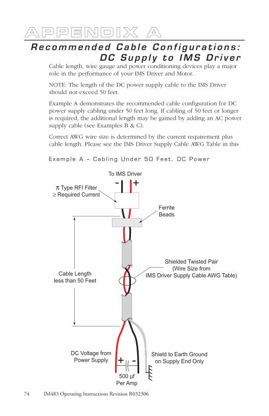
74 IM483 Operating Instructions Revision R032306 75IM483 Operating Instructions Revision R032306
A P P ENDIX aRecommended Cab l e C o n f i g u r a t i o n s :
DC Supp l y t o IMS D r i v e r Cable length, wire gauge and power conditioning devices play a major role in the performance of your IMS Driver and Motor.
NOTE: The length of the DC power supply cable to the IMS Driver should not exceed 50 feet.
Example A demonstrates the recommended cable configuration for DC power supply cabling under 50 feet long. If cabling of 50 feet or longer is required, the additional length may be gained by adding an AC power supply cable (see Examples B & C).
Correct AWG wire size is determined by the current requirement plus cable length. Please see the IMS Driver Supply Cable AWG Table in this
π
≥
E x amp l e A – C a b l i n g Und e r 50 F e e t , DC P owe r

74 IM483 Operating Instructions Revision R032306 75IM483 Operating Instructions Revision R032306
π≥
E x amp l e B – C a b l i n g 50 F e e t o r G r e a t e r, AC P owe r t o F u l l Wa v e B r i d g e
76 IM483 Operating Instructions Revision R032306 77IM483 Operating Instructions Revision R032306
π≥
E x amp l e C – C a b l i n g 50 F e e t o r G r e a t e r, AC P owe r t o P owe r S u p p l y

76 IM483 Operating Instructions Revision R032306 77IM483 Operating Instructions Revision R032306
IMS Driver Supply Cable AWG Table
1 Ampere (Peak)
2 Amperes (Peak)
3 Amperes (Peak)
4 Amperes (Peak)
Length (Feet)
Minimum AWG
Length (Feet)
Minimum AWG
Length (Feet)
Minimum AWG
Length (Feet)
Minimum AWG
10 25 50* 75* 100*
10 25 50* 75* 100*
10 25 50* 75* 100*
10 25 50* 75* 100*
20 20 18 18 16
20 18 16 14 14
18 16 14 12 12
18 16 14 12 12* Use the alternative methods innustrated inExamples B and C when the cable length is ≥ 50feet. Also, use the same current rating when thealternate AC power is used.
Driver Supply Cable Wire Size
NOTE: These recommendations will provide optimalprotection against EMI and RFI. The actual cable type,wire gauge, shield type and filtering devices used are de-pendent on the customer’s application and system.
NOTE: Always use Shielded/Twisted Pairs for the IMS Driver DC Supply Cable, the AC Supply Cable and the IMS Driver to Motor Cable.

78 IM483 Operating Instructions Revision R032306 79IM483 Operating Instructions Revision R032306
Cable length, wire gauge and power conditioning devices play a major role in the performance of your IMS Driver and Motor.
NOTE: The length of the DC power supply cable between the IMS Driver and the Motor should not exceed 50 feet.
Example A demonstrates the recommended cable configuration for the IMS Driver to Motor cabling under 50 Feet long. If cabling of 50 feet or longer is required, the additional length can be gained with the cable configuration in Example B.
Correct AWG wire size is determined by the current requirement plus cable length. Please see the IMS Driver to Motor Cable AWG Table in this Appendix.
E x amp l e A - C a b l i n g Und e r 50 F e e t , IMS D r i v e r t o Mo t o r
Recommended Cab l e C o n f i g u r a t i o n s : IMS D r i v e r t o Mo t o r

78 IM483 Operating Instructions Revision R032306 79IM483 Operating Instructions Revision R032306
≈
E x amp l e B - C a b l i n g 50 F e e t o r G r e a t e r, IMS D r i v e r t o Mo t o r
80 IM483 Operating Instructions Revision R032306
1 Ampere (Peak)
Length (Feet)
Minimum AWG
10 25 50* 75* 100*
20 20 18 18 16
2 Amperes (Peak)
Length (Feet)
Minimum AWG
10 25 50* 75* 100*
20 18 16 14 14
3 Amperes (Peak)
Length (Feet)
Minimum AWG
10 25 50* 75* 100*
18 16 14 12 12
4 Amperes (Peak)
Length (Feet)
Minimum AWG
10 25 50* 75* 100*
18 16 14 12 12
5 Amperes (Peak)
Length (Feet)
Minimum AWG
10 25 50* 75* 100*
16 16 14 12 12
6 Amperess (Peak)
Length (Feet)
Minimum AWG
10 25 50* 75* 100*
14 14 14 12 12
7 Amperess (Peak)
Length (Feet)
Minimum AWG
10 25 50* 75* 100*
12 12 12 12 12
* Use the alternate method illustrated in Example Bwhen cable length is ≥ 50 feet.
IMS Driver to Motor Cable AWG Table
Driver to Motor Supply Cable Wire Size
NOTE: These recommendations will provide optimalprotection against EMI and RFI. The actual cable type,wire gauge, shield type and filtering devices used are de-pendent on the customer’s application and system.
NOTE: Always use Shielded/Twisted Pairs for the IMS Driver DC Supply Cable, the AC Supply Cable and the IMS Driver to Motor Cable.

WARRANTYTWENTY-FOUR (24) MONTH LIMITED WARRANTYIntelligent Motion Systems, Inc. (“IMS”), warrants only to the purchaser of the Product from IMS (the “Customer”) that the product purchased from IMS (the “Product”) will be free from defects in materials and workmanship under the normal use and service for which the Product was designed for a period of 24 months from the date of purchase of the Product by the Customer. Customer’s exclusive remedy under this Limited Warranty shall be the repair or replacement, at Company’s sole option, of the Product, or any part of the Product, determined by IMS to be defective. In order to exercise its warranty rights, Customer must notify Company in accordance with the instructions described under the heading “Obtaining Warranty Service.”
This Limited Warranty does not extend to any Product damaged by reason of alteration, accident, abuse, neglect or misuse or improper or inadequate handling; improper or inadequate wiring utilized or installed in connection with the Product; installation, operation or use of the Product not made in strict accordance with the specifications and written instructions provided by IMS; use of the Product for any purpose other than those for which it was designed; ordinary wear and tear; disasters or Acts of God; unauthorized attachments, alterations or modifications to the Product; the misuse or failure of any item or equipment connected to the Product not supplied by IMS; improper maintenance or repair of the Product; or any other reason or event not caused by IMS.
IMS HEREBY DISCLAIMS ALL OTHER WARRANTIES, WHETHER WRITTEN OR ORAL, EXPRESS OR IMPLIED BY LAW OR OTHERWISE, INCLUDING WITHOUT LIMITATION, ANY WARRANTIES OF MERCHANTABILITY OR FITNESS FOR ANY PARTICULAR PURPOSE. CUSTOMER’S SOLE REMEDY FOR ANY DEFECTIVE PRODUCT WILL BE AS STATED ABOVE, AND IN NO EVENT WILL THE IMS BE LIABLE FOR INCIDENTAL, CONSEQUENTIAL, SPECIAL OR INDIRECT DAMAGES IN CONNECTION WITH THE PRODUCT.
This Limited Warranty shall be void if the Customer fails to comply with all of the terms set forth in this Limited Warranty. This Limited Warranty is the sole warranty offered by IMS with respect to the Product. IMS does not assume any other liability in connection with the sale of the Product. No representative of IMS is authorized to extend this Limited Warranty or to change it in any manner whatsoever. No warranty applies to any party other than the original Customer.
IMS and its directors, officers, employees, subsidiaries and affiliates shall not be liable for any damages arising from any loss of equipment, loss or distortion of data, loss of time, loss or destruction of software or other property, loss of production or profits, overhead costs, claims of third parties, labor or materials, penalties or liquidated damages or punitive damages, whatsoever, whether based upon breach of warranty, breach of contract, negligence, strict liability or any other legal theory, or other losses or expenses incurred by the Customer or any third party.
OBTAINING WARRANTY SERVICEWarranty service may obtained by a distributor, if the Product was purchased from IMS by a distributor, or by the Customer directly from IMS, if the Product was purchased directly from IMS. Prior to returning the Product for service, a Returned Material Authorization (RMA) number must be obtained. Complete the form at http://www.imshome.com/rma.html after which an RMA Authorization Form with RMA number will then be faxed to you. Any questions, contact IMS Customer Service (860) 295-6102.
Include a copy of the RMA Authorization Form, contact name and address, and any additional notes regarding the Product failure with shipment. Return Product in its original packaging, or packaged so it is protected against electrostatic discharge or physical damage in transit. The RMA number MUST appear on the box or packing slip. Send Product to: Intelligent Motion Systems, Inc., 370 N. Main Street, Marlborough, CT 06447.
Customer shall prepay shipping changes for Products returned to IMS for warranty service and IMS shall pay for return of Products to Customer by ground transportation. However, Customer shall pay all shipping charges, duties and taxes for Products returned to IMS from outside the United States.

370 N. Main StreetP.O. Box 457Marlborough, CT 06447 U.S.A.Phone: 860/295-6102Fax: 860/295-6107E-mail: [email protected]
IMS MOTORS DIVISION 105 Copperwood Way, Suite H Oceanside, CA 92054 Phone: 760/966-3162 Fax: 760/966-3165 E-mail: [email protected]
U.S.A. SALES OFFICESEastern Region Phone: 862/208-9742 Fax: 973/661-1275 E-mail: [email protected] Region Phone: 260/402-6016 Fax: 419/858-0375 E-mail: [email protected] Region Phone: 408/472-1971 Fax: 408/268-0716 E-mail: [email protected]
ASIA PACIFIC OFFICE 30 Raffles Pl., 23-00 Caltex House Singapore 048622 Phone: +65/6233/6846 Fax: +65/6233/5044 E-mail: [email protected]
IMS EUROPE GmbH Hahnstrasse 10, VS-Schwenningen Germany D-78054 Phone: +49/7720/94138-0 Fax: +49/7720/94138-2 E-mail: [email protected] Sales Management 4 Quai Des Etroits 69005 Lyon, France Phone: +33/4 7256 5113 Fax: +33/4 7838 1537 E-mail: [email protected] Sales Phone: +49/35205/4587-8 Fax: +49/35205/4587-9 E-mail: [email protected]/UK Technical Support Phone: +49/7720/94138-0 Fax: +49/7720/94138-2 E-mail: [email protected]
IMS Product Disclaimer and most up-to-date product information available at www.imshome.com.© 2006 Intelligent Motion Systems, Inc. All Rights Reserved.
TECHNICAL SUPPORTEastern U.S.A. Phone: 860/295-6102 Fax: 860/295-6107 E-mail: [email protected] U.S.A. Phone: 760/966-3162 Fax: 760/966-3165 E-mail: [email protected]/UK Phone: +49/7720/94138-0 Fax: +49/7720/94138-2 E-mail: [email protected]
www.imshome.com